Quantum electrodynamics near a photonic...
6
LETTERS PUBLISHED ONLINE: 1 AUGUST 2016 | DOI: 10.1038/NPHYS3834 Quantum electrodynamics near a photonic bandgap Yanbing Liu and Andrew A. Houck * Photonic crystals are a powerful tool for the manipulation of op- tical dispersion and density of states, and have thus been used in applications from photon generation to quantum sensing with nitrogen vacancy centres and atoms 1,2 . The unique control provided by these media makes them a beautiful, if unexplored, playground for strong-coupling quantum electrodynamics, where a single, highly nonlinear emitter hybridizes with the band structure of the crystal. Here we demonstrate that such a hybridization can create localized cavity modes that live within the photonic bandgap, whose localization and spectral properties we explore in detail. We then demonstrate that the coloured vacuum of the photonic crystal can be employed for ecient dissipative state preparation. This work opens exciting prospects for engineering long-range spin models 3,4 in the circuit quantum electrodynamics architecture, as well as new opportunities for dissipative quantum state engineering. The perturbative effect of a structured vacuum is the renowned Purcell effect, which states that the lifetime of an atom in such a space will be proportional to the local photonic density of states (DOS) near the atomic transition frequency. In practice, the birth of the photonic crystal, which greatly modifies the vacuum fluctuations, has enabled the control of spontaneous emission of various emitters, such as quantum dots 5,6 , magnons 7 and superconducting qubits 8 . However, when an atom is strongly coupled to a photonic crystal, non-perturbative effects become important, and significantly enrich the physics. For instance, a single-photon bound state has been predicted to emerge within the gap 9 , and spontaneous emission of the atom will thus exhibit Rabi oscillation and light-trapping behaviour. In contrast to electronic bandgap systems, even multiple photons can be simultaneously localized by a single atom, and the coherent photonic transport within the otherwise forbidden bandgap can have a strongly correlated nature 10–12 . In contrast to a system with discrete cavity modes, which is well described by the single-mode or multimode Jaynes–Cummings Hamiltonian 13,14 , a continuous density of states enables the formation of a localized state in the bandgap. While other spin-boson problems with continuous DOS have also been studied experimentally 15,16 or theoretically 17,18 with superconducting circuits, this work explores physics near the band edge, where localized states emerge and reservoir engineering becomes possible. Light–matter interactions are being actively pursued using cold atoms coupled to optical photonic crystals 19,20 , where the study of photonic band edge effects requires a combination of challenging nanostructure fabrication and optical laser trapping. Although impressive progress has been made, atoms are only weakly coupled to photonic crystal waveguides 20 , potentially limiting the physics to the perturbative regime. In this letter, using a microwave photonic crystal and a superconducting transmon qubit, we are able to reach the strong-coupling regime of quantum electrodynamics near a photonic bandgap. This regime is characterized by the emergence of spectrally resolvable new polariton states, similar to the well- known vacuum Rabi splitting in cavity quantum electrodynamics. We will give a more quantitative definition of strong coupling in the following discussion. Our device consists of 14 unit cells, each of which contains two coplanar waveguide (CPW) sections with different lengths ‘ and impedances Z (‘ lo = 0.45 mm, ‘ hi = 8 mm and Z lo = 28 , Z hi = 125 ). These parameters are chosen so that the band edge is within our measurement window (4–10 GHz) and that the bare photonic crystal has a smooth spectrum. The dispersion relation can be calculated using transfer matrices and is given by cos ω k ‘ lo v p ! cos ω k ‘ hi v p ! - 1 2 Z hi Z lo + Z lo Z hi sin ω k ‘ lo v p ! × sin ω k ‘ hi v p ! = cos(k(‘ lo + ‘ hi )) (1) where v p is the phase velocity in the waveguide, ω k is the frequency of the allowed Bloch wave and k is the wavevector in the Brillouin zone. Based on the electric field distribution (Bloch wavefunction), we have purposely placed a transmon qubit in the centre of one unit cell in the middle of the device. This makes the qubit optimally coupled to the second photonic band. Consequently, only this band is taken into account, and a quadratic dispersion relation E = ¯ hω 0 + α(k - k 0 ) 2 is further assumed. Our device parameters yield ω 0 /2π = 7.7 GHz. The complete device image is shown in Fig. 1. It is anchored to the base stage (15mK) of our dilution refrigerator and connected to a typical 50 measurement chain. The Hamiltonian of the whole system can be written as H = X k ¯ hω k a † k a k + ¯ h ω q 2 σ z + X k ¯ hg k (a † k σ - + a k σ + ) (2) where ω q , ω k are the frequencies of the bare qubit and the electromagnetic mode with wavevector k. a † k (σ + ) and a k (σ - ) are the mode (qubit) raising and lowering operators. We have ignored other dissipation channels of the qubit and have also performed a rotating wave approximation. In the single-particle spectrum, there exists a polariton state within the bandgap with the eigenenergy ω b given by the root of the equation ¯ h(ω q - ω b ) √ ¯ h(ω 0 - ω b ) = πg 2 /α (3) We have already assumed that g k ≈ g for all wavevectors k, which is valid in our device design. The solution in the bandgap always exists no matter how far the bare qubit frequency ω q is detuned from the band edge ω 0 . In real space, the photonic part of this polariton state is exponentially localized around the qubit (hence the Department of Electrical Engineering, Princeton University, New Jersey 08544, USA. *e-mail: [email protected] NATURE PHYSICS | ADVANCE ONLINE PUBLICATION | www.nature.com/naturephysics 1 © 2016 Macmillan Publishers Limited. All rights reserved
-
Upload
truonghanh -
Category
Documents
-
view
214 -
download
0
Transcript of Quantum electrodynamics near a photonic...
LETTERSPUBLISHED ONLINE: 1 AUGUST 2016 | DOI: 10.1038/NPHYS3834
Quantum electrodynamics near aphotonic bandgapYanbing Liu and Andrew A. Houck*Photonic crystals areapowerful tool for themanipulationofop-tical dispersion and density of states, and have thus been usedin applications from photon generation to quantum sensingwith nitrogen vacancy centres and atoms1,2. The unique controlprovidedby thesemediamakes themabeautiful, if unexplored,playground for strong-coupling quantum electrodynamics,where a single, highly nonlinear emitter hybridizes with theband structure of the crystal. Here we demonstrate that sucha hybridization can create localized cavity modes that livewithin the photonic bandgap, whose localization and spectralproperties we explore in detail. We then demonstrate thatthe coloured vacuum of the photonic crystal can be employedfor ecient dissipative state preparation. This work opensexciting prospects for engineering long-range spinmodels3,4 inthe circuit quantum electrodynamics architecture, as well asnew opportunities for dissipative quantum state engineering.
The perturbative effect of a structured vacuum is the renownedPurcell effect, which states that the lifetime of an atom in sucha space will be proportional to the local photonic density ofstates (DOS) near the atomic transition frequency. In practice,the birth of the photonic crystal, which greatly modifies thevacuum fluctuations, has enabled the control of spontaneousemission of various emitters, such as quantum dots5,6, magnons7and superconducting qubits8. However, when an atom is stronglycoupled to a photonic crystal, non-perturbative effects becomeimportant, and significantly enrich the physics. For instance, asingle-photon bound state has been predicted to emerge within thegap9, and spontaneous emission of the atom will thus exhibit Rabioscillation and light-trapping behaviour. In contrast to electronicbandgap systems, even multiple photons can be simultaneouslylocalized by a single atom, and the coherent photonic transportwithin the otherwise forbidden bandgap can have a stronglycorrelated nature10–12. In contrast to a system with discrete cavitymodes, which is well described by the single-mode or multimodeJaynes–Cummings Hamiltonian13,14, a continuous density of statesenables the formation of a localized state in the bandgap. Whileother spin-boson problems with continuous DOS have also beenstudied experimentally15,16 or theoretically17,18 with superconductingcircuits, this work explores physics near the band edge, wherelocalized states emerge and reservoir engineering becomes possible.
Light–matter interactions are being actively pursued using coldatoms coupled to optical photonic crystals19,20, where the study ofphotonic band edge effects requires a combination of challengingnanostructure fabrication and optical laser trapping. Althoughimpressive progress has been made, atoms are only weakly coupledto photonic crystal waveguides20, potentially limiting the physics tothe perturbative regime. In this letter, using a microwave photoniccrystal and a superconducting transmon qubit, we are able to reachthe strong-coupling regime of quantum electrodynamics near aphotonic bandgap. This regime is characterized by the emergence
of spectrally resolvable new polariton states, similar to the well-known vacuum Rabi splitting in cavity quantum electrodynamics.We will give a more quantitative definition of strong coupling in thefollowing discussion.
Our device consists of 14 unit cells, each of which containstwo coplanar waveguide (CPW) sections with differentlengths ` and impedances Z (`lo = 0.45 mm, `hi = 8mm andZlo=28,Zhi=125). These parameters are chosen so that theband edge is within our measurement window (4–10GHz) and thatthe bare photonic crystal has a smooth spectrum. The dispersionrelation can be calculated using transfer matrices and is given by
cos
(ωk`lo
vp
)cos
(ωk`hi
vp
)−
12
(Zhi
Zlo+
Zlo
Zhi
)sin
(ωk`lo
vp
)
× sin
(ωk`hi
vp
)=cos(k(`lo+`hi)) (1)
where vp is the phase velocity in the waveguide, ωk is the frequencyof the allowed Bloch wave and k is the wavevector in the Brillouinzone. Based on the electric field distribution (Bloch wavefunction),we have purposely placed a transmon qubit in the centre of oneunit cell in the middle of the device. This makes the qubit optimallycoupled to the second photonic band. Consequently, only thisband is taken into account, and a quadratic dispersion relationE= hω0+α(k−k0)2 is further assumed. Our device parametersyield ω0/2π= 7.7GHz. The complete device image is shown inFig. 1. It is anchored to the base stage (15mK) of our dilutionrefrigerator and connected to a typical 50measurement chain.
The Hamiltonian of the whole system can be written as
H=∑k
hωka†kak+ h
ωq
2σ
z+∑k
hgk(a†kσ−+akσ+) (2)
where ωq, ωk are the frequencies of the bare qubit and theelectromagnetic mode with wavevector k. a†
k(σ+) and ak(σ−) are
the mode (qubit) raising and lowering operators. We have ignoredother dissipation channels of the qubit and have also performed arotating wave approximation. In the single-particle spectrum, thereexists a polariton state within the bandgap with the eigenenergy ωbgiven by the root of the equation
h(ωq−ωb)√h(ω0−ωb)=πg 2
/α (3)
We have already assumed that gk≈ g for all wavevectors k, whichis valid in our device design. The solution in the bandgap alwaysexists no matter how far the bare qubit frequency ωq is detunedfrom the band edge ω0. In real space, the photonic part of thispolariton state is exponentially localized around the qubit (hence the
Department of Electrical Engineering, Princeton University, New Jersey 08544, USA. *e-mail: [email protected]
NATURE PHYSICS | ADVANCE ONLINE PUBLICATION | www.nature.com/naturephysics 1
© 2016 Macmillan Publishers Limited. All rights reserved

LETTERS NATURE PHYSICS DOI: 10.1038/NPHYS3834
1 mm
−π/d π/d0k d
Freq
uenc
y (G
Hz)
28 Ω 28 Ω 125 Ω
3 μm
60 μm
47 μm
2 μm
Input Output
0.1 mm
0
5
10
a
d e
b
c
Figure 1 | Device design. a, Optical image of the device. The tan region indicates metals Nb and Al, while the black region indicates the sapphire substrate.The impedance is periodically modulated by varying the centre pin and gap widths of the CPW. b, A standard transmon qubit made with a split pair ofJosephson junctions is coupled to the high-impedance section of the unit cell in the middle of the device. c, High- and low-impedance sections of thewaveguide. d, Theoretical band structure of the 1D photonic crystal. e, Schematic of the qubit and the unit cell of the photonic crystal. The green and redcurves represent the calculated Bloch wavefunction at k=π/d of the first and the second photonic band, respectively. Placing the qubit in the middle of theunit cell maximizes(minimizes) the coupling with the second(first) band.
bound state) with the localization length L given by the penetrationdepth L=
√α/h(ω0−ωb). The qubit component of this state can be
computed to be Pq= 2(ωb−ω0)/(3ωb−ωq− 2ω0), therefore thisstate is mostly qubit-like deep within the bandgap, while it is mostlyphoton-like close to the band edge.
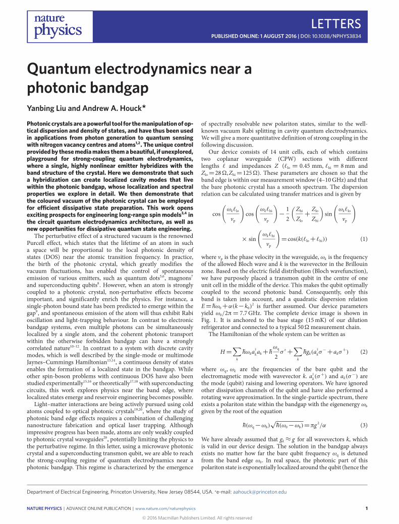
In an infinite photonic crystal, this bound state can result inpermanent light trapping12 in photonic transport. However, in ourfinite system, the size of which is comparable to L, it is a leaky boundstate with a finite spectral linewidth γ . It can be shown21 that γis proportional to the overlap of this state’s wavefunction with theexternally coupled waveguide γ ∼ e−d0/2L, where d0 is the physicallength of the device. When probed with a weak signal, this stateassists photonic transport within the bandgap; hence, we observea Lorentzian transmission peak centred at ωb. As the bare qubitfrequency ωq is tuned closer to the band edge, the bound state has alarger localization length, and thus carries a larger linewidth.
We measure the bound state linewidth γ and exponentially fitthe data to the calculated inverse localization length 1/L (Fig. 2b).
This yields the effective device length dfit to be 140 ± 12mm,in agreement with the length of the whole device d0 = 126mm.To further validate the above theoretical model, we focus on thecases where the bare qubit frequency is completely within theband. In Fig. 2a, we observe that the bound state peak belowthe band edge persists while the input signal at the bare qubitfrequency is completely reflected due to destructive interference15.Now we can extract ωq,ωb and fit the data to equation (3). Notethat when the bare qubit is resonant with the band edge, thepredicted energy shift is ∆/2π= (ωb−ω0)/2π= (πg 2/α)2/3(1/h)and Pq=2/3. We use ∆/2π as the fitting parameter instead of gso that we can then define the strong-coupling regime as ∆ κ ,where κ characterizes the steepness of the band edge. In our device,the best fit yields ∆/2π=250MHz, while κ/2π≈ 26MHz (seeSupplementary Information).
Unlike harmonic defect states, this bound state can be used tocontrol quantum transport within the bandgap. We achieve thisby taking advantage of the anharmonic multilevel structure of the
2
© 2016 Macmillan Publishers Limited. All rights reserved
NATURE PHYSICS | ADVANCE ONLINE PUBLICATION | www.nature.com/naturephysics
NATURE PHYSICS DOI: 10.1038/NPHYS3834 LETTERS
Freq
uenc
y (G
Hz)
−2 −1 0 1 2
S21 (dB)
Band
Gap
Pq
1/L (m−1)
γ (M
Hz)
DataExp fit
6.5
7.0
7.5
8.0
8.5
a b
c
Flux bias (V)
−50
−20
−30
−40
20
40
60
80
100
120
5 10 15 20 25 30
6.5
7.0
q (G
Hz)
7.5
8.0
ω
b (GHz)ω
6.5 7.0 7.5
0.1
0.3
0.5
0.7
0.9
Figure 2 | Single-photon bound state. a, Low-power transmission of the device as the qubit is tuned across the band edge. The colour bar represents thetransmission amplitude on a log scale and the dashed line indicates the band edge ω0. The persistent peak in the gap indicates the single-photon boundstate. Note that the defect state at 8.36 GHz does not couple to the qubit. b, Relation between the bound state linewidth and the localization length L. Theerror bars of the linewidth data represent the standard deviation of the Lorentzian fit. Based on the theory in the main text, we exponentially fit thelinewidth data (see Supplementary Information). c, Relation between the bare qubit frequency and the qubit component with the bound state frequency.The blue curve is extrapolated based on fitting the data when the qubit is within the band.
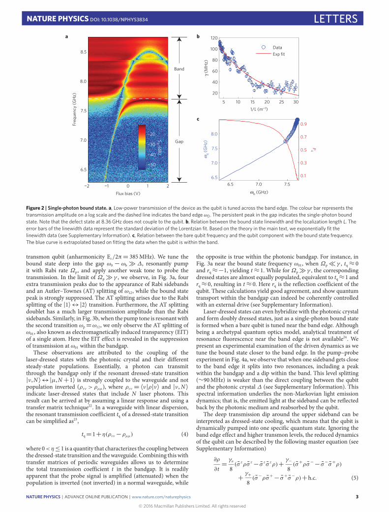
transmon qubit (anharmonicity Ec/2π= 385MHz). We tune thebound state deep into the gap ω0 − ωb ∆, resonantly pumpit with Rabi rate Ωp, and apply another weak tone to probe thetransmission. In the limit of Ωp γ , we observe, in Fig. 3a, fourextra transmission peaks due to the appearance of Rabi sidebandsand an Autler–Townes (AT) splitting of ω12, while the bound statepeak is strongly suppressed. The AT splitting arises due to the Rabisplitting of the |1〉↔|2〉 transition. Furthermore, the AT splittingdoublet has a much larger transmission amplitude than the Rabisidebands. Similarly, in Fig. 3b, when the pump tone is resonant withthe second transition ωp=ω12, we only observe the AT splitting ofω01, also known as electromagnetically induced transparency (EIT)of a single atom. Here the EIT effect is revealed in the suppressionof transmission at ω01 within the bandgap.
These observations are attributed to the coupling of thelaser-dressed states with the photonic crystal and their differentsteady-state populations. Essentially, a photon can transmitthrough the bandgap only if the resonant dressed-state transition|ν,N〉↔|µ,N+1〉 is strongly coupled to the waveguide and notpopulation inverted (ρνν > ρµµ), where ρνν = 〈ν|ρ|ν〉 and |ν,N〉indicate laser-dressed states that include N laser photons. Thisresult can be arrived at by assuming a linear response and using atransfer matrix technique22. In a waveguide with linear dispersion,the resonant transmission coefficient tq of a dressed-state transitioncan be simplified as23,
tq=1+η(ρνν−ρµµ) (4)
where 0<η≤1 is a quantity that characterizes the coupling betweenthe dressed-state transition and thewaveguide. Combining this withtransfer matrices of periodic waveguides allows us to determinethe total transmission coefficient t in the bandgap. It is readilyapparent that the probe signal is amplified (attenuated) when thepopulation is inverted (not inverted) in a normal waveguide, while
the opposite is true within the photonic bandgap. For instance, inFig. 3a near the bound state frequency ω01, when Ωp γ , tq≈ 0and rq≈−1, yielding t≈ 1. While for Ωpγ , the correspondingdressed states are almost equally populated, equivalent to tq≈1 andrq≈ 0, resulting in t≈ 0. Here rq is the reflection coefficient of thequbit. These calculations yield good agreement, and show quantumtransport within the bandgap can indeed be coherently controlledwith an external drive (see Supplementary Information).
Laser-dressed states can even hybridize with the photonic crystaland form doubly dressed states, just as a single-photon bound stateis formed when a bare qubit is tuned near the band edge. Althoughbeing a archetypal quantum optics model, analytical treatment ofresonance fluorescence near the band edge is not available24. Wepresent an experimental examination of the driven dynamics as wetune the bound state closer to the band edge. In the pump–probeexperiment in Fig. 4a, we observe that when one sideband gets closeto the band edge it splits into two resonances, including a peakwithin the bandgap and a dip within the band. This level splitting(∼90MHz) is weaker than the direct coupling between the qubitand the photonic crystal ∆ (see Supplementary Information). Thisspectral information underlies the non-Markovian light emissiondynamics; that is, the emitted light at the sideband can be reflectedback by the photonic medium and reabsorbed by the qubit.
The deep transmission dip around the upper sideband can beinterpreted as dressed-state cooling, which means that the qubit isdynamically pumped into one specific quantum state. Ignoring theband edge effect and higher transmon levels, the reduced dynamicsof the qubit can be described by the following master equation (seeSupplementary Information)
∂ρ
∂t=γo
8(σ
zρσ
z− σ
zσ
zρ)+
γ−
8(σ+ρσ−− σ
−σ+ρ)
+γ+
8(σ−ρσ+− σ
+σ−ρ)+h.c. (5)
NATURE PHYSICS | ADVANCE ONLINE PUBLICATION | www.nature.com/naturephysics
© 2016 Macmillan Publishers Limited. All rights reserved
3

LETTERS NATURE PHYSICS DOI: 10.1038/NPHYS3834
Pump power (dBm)
Prob
e fr
eque
ncy
(GH
z)
Prob
e fr
eque
ncy
(GH
z)−40 −30 −20 −10
Pump power (dBm)
−40 −30 −20 −10−55
−50
−45
−40
−35
−30
−25
6.8
6.9
p
7.0
7.1
7.2
7.3
7.4
a b
6.8
6.9
7.0
7.1
7.2
7.3
7.4
S21 (dB)
ω
pω
Figure 3 | Pump–probe experiment within the bandgap. The colour bar represents the transmission amplitude of the weak probe signal in log scale. Theinset shows the level diagram of the bare states and dressed states. a, The bound state is deep within the bandgap (ωp=ω01=7.206 GHz andω12=7.008 GHz). The transmission near the bound state frequency ω01 is strongly suppressed, accompanied by two Rabi sidebands at approximatelyω01±Ωp. The most prominent signature is the Autler–Townes splitting of the second transition near ω12. Dashed white lines indicate simulation results.Four transmon states are accounted for in the simulation, where the only fitting parameter is the eective Rabi rateΩp. b, ωp=ω12. In this case, the ATsplitting of ω01 is the dominant feature.
Freq
uenc
y (G
Hz)
−40 −20
−40
−50
−30
−20
Power (dBm)
Freq
uenc
y (G
Hz)
−16 −14 −12 −10 −8 −6
Sideband frequency s (GHz)
Simulation A
⎪+, n⟩
⎪+, n − 1⟩⎪−, n − 1⟩
⎪−, n⟩
Simulation B
−10
−5
0
5
Transmission dip
7.0
7.1
7.2
7.3
7.4
7.5
7.6
7.7
7.8
7.9
8.0
Power (dBm)
7.6
7.7
7.8
7.9
8.0
0.65
0.70
0.75
0.80
0.85
0.90
7.80 7.85 7.90 7.95 8.00ω
a b
c
+γ −γ
Stat
e pu
rity
−−
ρ
Figure 4 | Pump–probe experiment near the photonic band edge. a, ωp=ω01=7.44 GHz. Dashed lines indicate the band edge and dressed-statetransitions fitted with the same model as in Fig. 3. The sideband that falls within the photonic band in the top-right boxed region is further shown in b. Thecolour bar represents the transmission amplitude of the weak probe signal on a log scale. b, Zoom-in of the upper sideband. The new colour bar is found bysubtracting the bare photonic crystal transmission. Note the appearance of an additional resonance when the sideband is close to the band edge. Theresonance within the band is shown in strong attenuation of the probe signal. c, Simulated state purity ρ−− using two dierent methods (seeSupplementary Information). The inset shows the schematic of the dressed-state cooling when γ+γ−.
4
© 2016 Macmillan Publishers Limited. All rights reserved
NATURE PHYSICS | ADVANCE ONLINE PUBLICATION | www.nature.com/naturephysics

NATURE PHYSICS DOI: 10.1038/NPHYS3834 LETTERSHere the decay rates of Mollow triplets, γ0,±, are proportional tothe local photonic DOS and σ z ,+,− are Pauli matrices in the dressedstate |±〉= (1/
√2)(|0〉±|1〉) basis. It is clear that the steady-state
population of the dressed state |−〉 is ρ−− = γ+/(γ− + γ+). Asa result, the qubit will be polarized to the |−〉 state if the uppersideband falls in the photonic band while the lower sideband fallsin the bandgap (γ+ γ−). Linewidth data in Fig. 2a are used toestimate γ± in the system. Further taking into account the highertransmon level, we then approximate the dressed-state purity asρ−−≈ 1− 2γ−/γ+ (method A). Alternatively, the attenuation ofthe probe signal can be used to deduce ρ−−≈ 1− tq/2 based onthe above linear response theory (method B). Detailed quantitativeanalysis using these two methods is given in the SupplementaryInformation and the results are shown in Fig. 4c. Simulated ρ−−reaches a maximum of 83% near the band edge where γ+ is largest.
In comparison with a prior reservoir engineering approach inwhich a similar effect was demonstrated25, here only one externaldrive is required and the cooling effect is caused by the colouredvacuum of the photonic crystal. This mechanism could be usedto stabilize an arbitrary state on the Bloch sphere by detuning thedrive from the qubit. Future versions of the device can purposelyincorporate a defect cavity mode to assist dispersive readout ofthe qubit state and incorporate more unit cells to increase thecooling fidelity. Furthermore, this can be directly generalized tothe many-qubit case where a dynamical quantum phase transitionwould be observable and highly entangled many-body states canbe stabilized26,27. Also, by engineering the coupling of the qubitwith multiple bands, a potential wideband dressed-state laser andamplifier can be envisioned.
In the future, low-noise amplifiers can be integrated to studyquantum correlation effects in coherent multiphoton transport. Thesuperconducting transmon qubit can be replaced by a flux qubitto reach the ultrastrong-coupling regime28,29. The concept can begeneralized to three-dimensional architectures and other quantumemitters. Finally, this provides a platform for studying spin modelswith coupling mediated by overlapping photonics bound states3,4,with built-in initialization through reservoir engineering.
MethodsMethods, including statements of data availability and anyassociated accession codes and references, are available in theonline version of this paper.
Received 22 March 2016; accepted 21 June 2016;published online 1 August 2016
References1. Li, L. et al . Coherent spin control of a nanocavity-enhanced qubit in diamond.
Nature Commun. 6, 6173 (2015).2. Clevenson, H. et al . Broadband magnetometry and temperature sensing with a
light-trapping diamond waveguide. Nature Phys. 11, 393–397 (2015).3. Douglas, J. S. et al . Quantum many-body models with cold atoms coupled to
photonic crystals. Nature Photon. 9, 326–331 (2015).4. Gonzalez-Tudela, A., Hung, C.-L., Chang, D. E., Cirac, J. I. & Kimble, H. J.
Subwavelength vacuum lattices and atom–atom interactions intwo-dimensional photonic crystals. Nature Photon. 9, 320–325 (2015).
5. Lodahl, P. et al . Controlling the dynamics of spontaneous emission fromquantum dots by photonic crystal. Nature 430, 654–657 (2004).
6. Fujita, M., Takahashi, S., Tanaka, Y., Asano, T. & Noda, S. Simultaneousinhibition and redistribution of spontaneous light emission in photoniccrystals. Science 308, 1296–1298 (2005).
7. Hoeppe, U. et al . Direct observation of non-Markovian radiation dynamics in3D bulk photonic crystals. Phy. Rev. Lett. 108, 043603 (2012).
8. Bronn, N. T. et al . Broadband filters for abatement of spontaneous emission forsuperconducting qubits. Appl. Phys. Lett. 107, 172601 (2015).
9. John, S. & Wang, J. Quantum electrodynamics near a photonic band gap:photon bound states and dressed atoms. Phys. Rev. Lett. 64, 2418–2421 (1990).
10. Rupasov, V. I. & Singh, M. Quantum gap solitons and many-polariton-atombound states in dispersive medium and photonic band gap. Phys. Rev. Lett. 77,338–341 (1996).
11. John, S. & Rupasov, V. I. Multiphoton localization and propagating quantumgap solitons in a frequency gap medium. Phys. Rev. Lett. 79, 821–824 (1997).
12. Longo, P., Schmitteckert, P. & Busch, K. Few-photon transport inlow-dimensional systems: interaction-induced radiation trapping. Phys. Rev.Lett. 104, 023602 (2010).
13. Yoshie, T. et al . Vacuum Rabi splitting with a single quantum dot in a photoniccrystal nanocavity. Nature 432, 200–203 (2004).
14. Sundaresan, N. M. et al . Beyond strong coupling in a multimode cavity. Phys.Rev. X 5, 021035 (2015).
15. Astafiev, O. et al . Resonance fluorescence of a single artificial atom. Science327, 840–843 (2010).
16. Hoi, I.-C. et al . Generation of nonclassical microwave states using an artificialatom in 1D open space. Phys. Rev. Lett. 108, 263601 (2012).
17. Le Hur, K. Kondo resonance of a microwave photon. Phys. Rev. B 85,140506(R) (2012).
18. Goldstein, M., Devoret, M. H., Houzet, M. & Glazman, L. I. Inelasticmicrowave photon scattering off a quantum impurity in a Josephson-junctionarray. Phys. Rev. Lett. 110, 017002 (2013).
19. Thompson, J. D. et al . Coupling a single trapped atom to a nanoscale opticalcavity. Science 340, 1202–1205 (2013).
20. Goban, A. et al . Atom-light interactions in photonic crystal. Nature Commun.5, 3808 (2014).
21. Biondi, M., Schmidt, S., Blatter, G. & Tureci, H. E. Self-protected polaritonstates in photonic quantum metamaterials. Phys. Rev. A 89, 025801 (2014).
22. Shen, J. T. & Fan, S. Coherent single-photon transport in a one-dimensionalwaveguide coupled with superconducting quantum bits. Phys. Rev. Lett. 95,213001 (2005).
23. Koshino, K. et al . Observation of the three-state dressed states in circuitquantum electrodynamics. Phys. Rev. Lett. 110, 263601 (2013).
24. Breuer, H. P. & Petruccione, F. The Theory of Open Quantum Systems(Oxford Univ. Press, 2007).
25. Murch, K. W. et al . Cavity-assisted quantum bath engineering. Phys. Rev. Lett.109, 183602 (2012).
26. John, S. & Quang, T. Quantum optical spin-glass state of impurity two-levelatoms in a photonic band gap. Phys. Rev. Lett. 76, 1320–1323 (1996).
27. John, S. & Quang, T. Collective switching and inversion without fluctuationof two-level atoms in confined photonic systems. Phys. Rev. Lett. 78,1888–1891 (1997).
28. Yoshihara, F. et al . Superconducting qubit-oscillator circuit beyond theultrastrong-coupling regime. Preprint at http://arXiv.org/abs/1602.00415(2016).
29. Forn-Díaz, P. et al . Ultrastrong coupling of a single artificial atom to anelectromagnetic continuum. Preprint at http://arXiv.org/abs/1602.00416(2016).
AcknowledgementsThe authors would like to acknowledge D. Sadri, G. Zhang, N. M. Sundaresan andJ. Simon for valuable discussions. This work is supported by IARPA under contractW911NF-10-1-0324 and the US National Science Foundation through MaterialsResearch Science and Engineering Centers under contract DMR-1420541.
Author contributionsY.L. designed the device, performed the measurements and analysed the data. A.A.H.supervised the whole experiment. All authors contributed to the preparation ofthis manuscript.
Additional informationSupplementary information is available in the online version of the paper. Reprints andpermissions information is available online at www.nature.com/reprints.Correspondence and requests for materials should be addressed to A.A.H.
Competing financial interestsThe authors declare no competing financial interests.
NATURE PHYSICS | ADVANCE ONLINE PUBLICATION | www.nature.com/naturephysics
© 2016 Macmillan Publishers Limited. All rights reserved
5

LETTERS NATURE PHYSICS DOI: 10.1038/NPHYS3834
MethodsThe photonic crystal was made using standard optical lithography and dry etchingtechniques from a 200 nm Nb thin film on a 10mm×10mm sapphire substrate.The pair of Josephson junctions of the transmon qubit were made using the Dolanbridge technique and evaporated with aluminium. The whole device is packaged ina printed circuit board, wire bonded and anchored at the base plate (15mK) of our
dilution refrigerator. An external solenoid magnet is used to apply a magnetic fieldacross the SQUID loop of the qubit.
Data availability. The data that support the plots within this paper and otherfindings of this study are available from the corresponding author uponreasonable request.
© 2016 Macmillan Publishers Limited. All rights reserved
NATURE PHYSICS | www.nature.com/naturephysics