Quantization Noise Suppression in Fractional PLLs · Abstract: A novel programmable frequency...
10
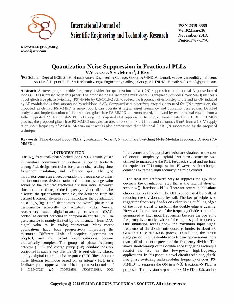
www.semargroups.org, www.ijsetr.com ISSN 2319-8885 Vol.02,Issue.16, November-2013, Pages:1767-1776 Copyright @ 2013 SEMAR GROUPS TECHNICAL SOCIETY. All rights reserved. Quantization Noise Suppression in Fractional PLLs V.VENKATA SIVA MOULI 1 , J.RAVI 2 1 PG Scholar, Dept of ECE, Sri Krishnadevaraya Engineering College, Gooty, AP-INDIA, E-mail: [email protected]. 2 Asst Prof, Dept of ECE, Sri Krishnadevaraya Engineering College, Gooty, AP-INDIA, E-mail: [email protected]. Abstract: A novel programmable frequency divider for quantization noise (QN) suppression in fractional-N phase-locked loops (PLLs) is presented in this paper. The proposed phase switching multi-modulus frequency divider (PS-MMFD) utilizes a novel glitch-free phase switching (PS) divide-by-0.5/1/1.5/2 cell to reduce the frequency division step to 0.5 and its QN induced by ΔΣ modulation is thus suppressed by additional 6 dB. Compared with other frequency dividers used for QN suppression, the proposed glitch-free PS-MMFD is more robust, can operate at higher input frequency and consumes less power. Detailed analysis and implementation of the proposed glitch-free PS-MMFD is demonstrated, followed by experimental results from a fully integrated ΔΣ fractional-N PLL utilizing the proposed QN suppression technique. Implemented in a 0.18 μm CMOS process, the proposed glitch-free PS-MMFD occupies an area of 0.38 mm × 0.25 mm and consumes 5 mA from a 1.8-V supply at an input frequency of 2 GHz. Measurement results also demonstrate the additional 6-dB QN suppression by the proposed technique. Keywords: Phase-Locked Loop (PLL), Quantization Noise (QN) and Phase Switching Multi-Modulus Frequency Divider (PS- MMFD). 1. INTRODUCTION The fractional- phase-locked loop (PLL) is widely used in wireless communication systems, allowing tradeoffs among PLL design constrains for phase noise, settling time, frequency resolution, and reference spur. The modulator generates a pseudo-random bit sequence to dither the instantaneous division ratio and its time-average value equals to the required fractional division ratio. However, since the internal step of the frequency divider still remains discrete, the quantization error, i.e., the deviation from the desired fractional division ratio, introduces the quantization noise (QN)(fig.1) and deteriorates the overall phase noise performance especially for wideband PLLs. Several researchers used digital-to-analog converter (DAC) controlled current branches to compensate for the QN. The performance is mainly limited by the mismatch from DAC digital value to its analog counterpart. Many recent publications have been progressively improving the mismatch. Different kinds of adaptive algorithms are adopted, and the circuit implementations become dramatically complex. The groups of phase frequency detector (PFD) and charge pump (CP) combinations are controlled in such a way that the QN is equivalently filtered out by a digital finite-impulse response (FIR) filter. Another noise filtering technique based on an integer- PLL in a feedback path suppresses out-of-band quantization noise of a high-order modulator. Nonetheless, both improvements of output phase noise are obtained at the cost of circuit complexity. Hybrid PFD/DAC structure was utilized to manipulate the PLL feedback signal and perform the equivalent QN compensation. However, such technique demands extremely high accuracy in timing control. The most straightforward way to suppress the QN is to decrease the quantization step that is the internal division step in fractional- PLLs. There are several publications elaborating on this idea. The QN is suppressed by 6 dB if reducing the division step by half. The key principle is to trigger the frequency divider on either rising or falling edges of the input signal to perform the double edge triggering. However, the robustness of the frequency divider cannot be guaranteed at high input frequencies because the operating frequency is actually twice of the input signal frequency. Our simulation results show the maximum input signal frequency of the divider introduced is limited to about 3.0 GHz in a 0.18 m CMOS process. In addition, the circuit stage performing the double edge triggering consumes more than half of the total power of the frequency divider. The above shortcomings of the double edge triggering technique restrict its use in the low-power high-frequency applications. In this paper, a novel circuit technique, glitch- free phase switching multi-modulus frequency divider (PS- MMFD) to suppress the QN in a fractional-N PLL, is proposed. The division step of the PS-MMFD is 0.5, and its
Transcript of Quantization Noise Suppression in Fractional PLLs · Abstract: A novel programmable frequency...
www.semargroups.org,
www.ijsetr.com
ISSN 2319-8885
Vol.02,Issue.16,
November-2013,
Pages:1767-1776
Copyright @ 2013 SEMAR GROUPS TECHNICAL SOCIETY. All rights reserved.
Quantization Noise Suppression in Fractional PLLs V.VENKATA SIVA MOULI
1, J.RAVI
2
1PG Scholar, Dept of ECE, Sri Krishnadevaraya Engineering College, Gooty, AP-INDIA, E-mail: [email protected].
2Asst Prof, Dept of ECE, Sri Krishnadevaraya Engineering College, Gooty, AP-INDIA, E-mail: [email protected].
Abstract: A novel programmable frequency divider for quantization noise (QN) suppression in fractional-N phase-locked
loops (PLLs) is presented in this paper. The proposed phase switching multi-modulus frequency divider (PS-MMFD) utilizes a
novel glitch-free phase switching (PS) divide-by-0.5/1/1.5/2 cell to reduce the frequency division step to 0.5 and its QN induced
by ΔΣ modulation is thus suppressed by additional 6 dB. Compared with other frequency dividers used for QN suppression, the
proposed glitch-free PS-MMFD is more robust, can operate at higher input frequency and consumes less power. Detailed
analysis and implementation of the proposed glitch-free PS-MMFD is demonstrated, followed by experimental results from a
fully integrated ΔΣ fractional-N PLL utilizing the proposed QN suppression technique. Implemented in a 0.18 μm CMOS
process, the proposed glitch-free PS-MMFD occupies an area of 0.38 mm × 0.25 mm and consumes 5 mA from a 1.8-V supply
at an input frequency of 2 GHz. Measurement results also demonstrate the additional 6-dB QN suppression by the proposed
technique.
Keywords: Phase-Locked Loop (PLL), Quantization Noise (QN) and Phase Switching Multi-Modulus Frequency Divider (PS-
MMFD).
1. INTRODUCTION
The fractional- phase-locked loop (PLL) is widely used
in wireless communication systems, allowing tradeoffs
among PLL design constrains for phase noise, settling time,
frequency resolution, and reference spur. The
modulator generates a pseudo-random bit sequence to dither
the instantaneous division ratio and its time-average value
equals to the required fractional division ratio. However,
since the internal step of the frequency divider still remains
discrete, the quantization error, i.e., the deviation from the
desired fractional division ratio, introduces the quantization
noise (QN)(fig.1) and deteriorates the overall phase noise
performance especially for wideband PLLs. Several
researchers used digital-to-analog converter (DAC)
controlled current branches to compensate for the QN. The
performance is mainly limited by the mismatch from DAC
digital value to its analog counterpart. Many recent
publications have been progressively improving the
mismatch. Different kinds of adaptive algorithms are
adopted, and the circuit implementations become
dramatically complex. The groups of phase frequency
detector (PFD) and charge pump (CP) combinations are
controlled in such a way that the QN is equivalently filtered
out by a digital finite-impulse response (FIR) filter. Another
noise filtering technique based on an integer- PLL in a
feedback path suppresses out-of-band quantization noise of
a high-order modulator. Nonetheless, both
improvements of output phase noise are obtained at the cost
of circuit complexity. Hybrid PFD/DAC structure was
utilized to manipulate the PLL feedback signal and perform
the equivalent QN compensation. However, such technique
demands extremely high accuracy in timing control.
The most straightforward way to suppress the QN is to
decrease the quantization step that is the internal division
step in fractional- PLLs. There are several publications
elaborating on this idea. The QN is suppressed by 6 dB if
reducing the division step by half. The key principle is to
trigger the frequency divider on either rising or falling edges
of the input signal to perform the double edge triggering.
However, the robustness of the frequency divider cannot be
guaranteed at high input frequencies because the operating
frequency is actually twice of the input signal frequency.
Our simulation results show the maximum input signal
frequency of the divider introduced is limited to about 3.0
GHz in a 0.18 m CMOS process. In addition, the circuit
stage performing the double edge triggering consumes more
than half of the total power of the frequency divider. The
above shortcomings of the double edge triggering technique
restrict its use in the low-power high-frequency
applications. In this paper, a novel circuit technique, glitch-
free phase switching multi-modulus frequency divider (PS-
MMFD) to suppress the QN in a fractional-N PLL, is
proposed. The division step of the PS-MMFD is 0.5, and its

V.VENKATA SIVA MOULI, J.RAVI
International Journal of Scientific Engineering and Technology Research
Volume.02, IssueNo.16, November-2013, Pages:1767-1776
QN induced by modulation is thus suppressed by
additional 6 dB. In addition, the PS-MMFD could operate at
a higher frequency since its internal operating frequency is
not doubled. Furthermore, a wide continuous frequency
division range is achieved in the proposed PS-MMFD by
using division ratio extension logic. A fractional- PLL
utilizing the proposed glitch-free PS-MMFD is also
designed and implemented in a 0.18 m CMOS process to
demonstrate its performance.
Fig.1 phase noise profile with and without QN suppression.
II. QUANTIZATION
In analog-to-digital conversion, the difference between
the actual analog value and quantized digital value is
called quantization error or quantization distortion. This
error is either due to rounding or truncation. The error signal
is sometimes considered as an additional random signal
called quantization noise (fig.2) because of its stochastic
behavior. Quantization is involved to some degree in nearly
all digital signal processing, as the process of representing a
signal in digital form ordinarily involves rounding.
Quantization also forms the core of essentially all lossy
compression algorithms.
Fig.2. original signal, quantized signal, quantization noise
A. Basic properties and types of quantization
Because quantization is a many-to-few mapping, it is an
inherently non-linear and irreversible process (i.e., because
the same output value is shared by multiple input values, it
is impossible in general to recover the exact input value
when given only the output value).
The set of possible input values may be infinitely large,
and may possibly be continuous and
therefore uncountable (such as the set of all real numbers, or
all real numbers within some limited range). The set of
possible output values may be finite or count ably infinite.
The input and output sets involved in quantization can be
defined in a rather general way. For example, vector
quantization is the application of quantization to multi-
dimensional (vector-valued) input data. There are two
substantially different classes of applications where
quantization is used: The first type, which may simply be
called rounding quantization, is the one employed for many
applications, to enable the use of a simple approximate
representation for some quantity that is to be measured and
used in other calculations. This category includes the simple
rounding approximations used in everyday arithmetic. This
category also includes analog-to-digital conversion of a
signal for a digital signal processing system (e.g., using a
sound card of a personal computer to capture an audio
signal) and the calculations performed within most digital
filtering processes. Here the purpose is primarily to retain as
much signal fidelity as possible while eliminating
unnecessary precision and keeping the dynamic range of the
signal within practical limits (to avoid signal clipping or
arithmetic overflow). In such uses, substantial loss of signal
fidelity is often unacceptable, and the design often centers
around managing the approximation error to ensure that
very little distortion is introduced.
The second type, which can be called rate–distortion
optimized quantization, is encountered in source coding for
" lossy " data compression algorithms, where the purpose is
to manage distortion within the limits of the bit rate
supported by a communication channel or storage medium.
In this second setting, the amount of introduced distortion
may be managed carefully by sophisticated techniques, and
introducing some significant amount of distortion may be
unavoidable. A quantize designed for this purpose may be
quite different and more elaborate in design than an ordinary
rounding operation. It is in this domain that substantial rate–
distortion theory analysis is likely to be applied. However,
the same concepts actually apply in both use cases. The
analysis of quantization involves studying the amount of
data (typically measured in digits or bits or bit rate) that is
used to represent the output of the quantize, and studying
the loss of precision that is introduced by the quantization
process (which is referred to as the distortion). The general
field of such study of rate and distortion is known as rate–
distortion theory.
B. Scalar quantization
The most common type of quantization is known
as scalar quantization. Scalar quantization, typically denoted
as is the process of using a quantization
function to map a scalar (one-dimensional) input

Quantization Noise Suppression in Fractional PLLs
International Journal of Scientific Engineering and Technology Research
Volume.02, IssueNo.16, November-2013, Pages:1767-1776
value to a scalar output value . Scalar quantization can
be as simple and intuitive as rounding high-precision
numbers to the nearest integer, or to the nearest multiple of
some other unit of precision (such as rounding a large
monetary amount to the nearest thousand dollars). Scalar
quantization of continuous-valued input data that is
performed by an electronic sensor is referred to as analog-
to-digital conversion. Analog-to-digital conversion often
also involves sampling the signal periodically in time (e.g.,
at 44.1 k Hz for CD-quality audio signals).
C. Rounding example
As an example, rounding a real number to the nearest
integer value forms a very basic type of quantize a uniform
one. A typical (mid-tread) uniform quantize with a
quantization step size equal to some value △ can be
expressed as
, (1)
Where the function ( ) is the sign function (also
known as the signum function). For simple rounding to the
nearest integer, the step size △ is equal to 1. With or
with △ equal to any other integer value, this quantize has
real-valued inputs and integer-valued outputs, although this
property is not a necessity a quantize may also have an
integer input domain and may also have non-integer output
values. The essential property of a quantize is that it has a
countable set of possible output values that has fewer
members than the set of possible input values. The members
of the set of output values may have integer, rational, or real
values (or even other possible values as well, in general –
such as vector values or complex numbers).
When the quantization step size is small (relative to the
variation in the signal being measured), it is relatively
simple to show that the mean squared error produced by
such a rounding operation will be approximately .
Because the set of possible output values of a quantize is
countable, any quantize can be decomposed into two distinct
stages, which can be referred to as the classification stage
(or forward quantization stage) and the reconstruction stage
(or inverse quantization stage), where the classification
stage maps the input value to an integer quantization index
and the reconstruction stage maps the index to
the reconstruction value that is the output approximation
of the input value. For the example uniform quantizer
described above, the forward quantization stage can be
expressed as
, (2)
And the reconstruction stage for this example quantize is
simply , This decomposition is useful for the
design and analysis of quantization behavior, and it
illustrates how the quantized data can be communicated
over a communication channel – a source encoder can
perform the forward quantization stage and send the index
information through a communication channel (possibly
applying entropy coding techniques to the quantization
indices), and a decoder can perform the reconstruction stage
to produce the output approximation of the original input
data. In more elaborate quantization designs, both the
forward and inverse quantization stages may be
substantially more complex. In general, the forward
quantization stage may use any function that maps the input
data to the integer space of the quantization index data, and
the inverse quantization stage can conceptually (or literally)
be a table look-up operation to map each quantization index
to a corresponding reconstruction value. This two-stage
decomposition applies equally well to vector as well as
scalar quantizers.
D. Mid-riser and mid-tread uniform quantizers
Most uniform quantizers for signed input data can be
classified as being of one of two types: mid-riser and mid-
tread. The terminology is based on what happens in the
region around the value 0, and uses the analogy of viewing
the input-output function of the quantizer as a stairway.
Mid-tread quantizers have a zero-valued reconstruction
level (corresponding to a tread of a stairway), while mid-
riser quantizers have a zero-valued classification threshold
(corresponding to a riser of a stairway). The formulas for
mid-tread uniform quantization are provided above. The
input-output formula for a mid-riser uniform quantizer is
given by:
, (3)
Where the classification rule is given by
(4)
And the reconstruction rule is
(5)
Note that mid-riser uniform quantizers do not have a zero
output value – their minimum output magnitude is half the
step size. When the input data can be modeled as a random
variable with a probability density function (pdf ) that is
smooth and symmetric around zero, mid-riser quantizers
also always produce an output entropy of at least 1 bit per
sample.
In contrast, mid-tread quantizers do have a zero output
level, and can reach arbitrarily low bit rates per sample for
input distributions that are symmetric and taper off at higher
magnitudes. For some applications, having a zero output
signal representation or supporting low output entropy may
be a necessity. In such cases, using a mid-tread uniform
quantize may be appropriate while using a mid-riser one
would not be. In general, a mid-riser or mid-tread quantize
may not actually be a uniform quantize – i.e., the size of the
quantizer's classification intervals may not all be the same,
or the spacing between its possible output values may not all
be the same. The distinguishing characteristic of a mid-riser

V.VENKATA SIVA MOULI, J.RAVI
International Journal of Scientific Engineering and Technology Research
Volume.02, IssueNo.16, November-2013, Pages:1767-1776
quantize is that it has a classification threshold value that is
exactly zero, and the distinguishing characteristic of a mid-
tread quantize is that is it has a reconstruction value that is
exactly zero. Another name for a mid-tread quantize
is dead-zone quantize, and the classification region around
the zero output value of such a quantize is referred to as
the dead zone. The dead zone can sometimes serve the same
purpose as a noise gate or squelch function.
E. The additive noise model for quantization error
A common assumption for the analysis of quantization
error is that it affects a signal processing system in a similar
manner to that of additive white noise – having negligible
correlation with the signal and an approximately flat power
spectral density. The additive noise model is commonly
used for the analysis of quantization error effects in digital
filtering systems, and it can be very useful in such analysis.
It has been shown to be a valid model in cases of high
resolution quantization (small △ relative to the signal
strength) with smooth probability density functions.
However, additive noise behavior is not always a valid
assumption, and care should be taken to avoid assuming that
this model always applies. In actuality, the quantization
error (for quantizers defined as described here) is
deterministically related to the signal rather than being
independent of it, and in some cases it can even cause limit
cycles to appear in digital signal processing systems. One
way to ensure effective independence of the quantization
error from the source signal is to perform dithered
quantization(sometimes with noise shaping), which involves
adding random (or pseudo-random) noise to the signal prior
to quantization. This can sometimes be beneficial for such
purposes as improving the subjective quality of the result;
however it can increase the total quantity of error introduced
by the quantization process.
F. Quantization error models
In the typical case, the original signal is much larger than
one least significant bit (LSB). When this is the case, the
quantization error is not significantly correlated with the
signal, and has an approximately uniform distribution. In the
rounding case, the quantization error has a mean of zero and
the RMS value is the standard deviation of this distribution,
given by . In the truncation case the error
has a non-zero mean of and the RMS value is .
In the eight-bit ADC example, the RMS rounding error
represents 0.113% of the full signal range. At lower
amplitudes the quantization error becomes dependent on the
input signal, resulting in distortion. This distortion is created
after the anti-aliasing filter, and if these distortions are
above 1/2 the sample rate they will alias back into the band
of interest. In order to make the quantization error
independent of the input signal, noise with amplitude of 2
least significant bits is added to the signal. This slightly
reduces signal to noise ratio, but, ideally, completely
eliminates the distortion. It is known as dither.
III. QUANTIZATION NOISE MODEL
Fig. 3. Original and Quantized signal, Quantization Error
Quantization noise for a 2-bit ADC operating at infinite
sample rate. The difference between the blue and red signals
in the upper graph is the quantization error(fig.3), which is
"added" to the quantized signal and is the source of noise.
Quantization noise is a model of quantization error
introduced by quantization in the analog-to-digital
conversion(ADC) in telecommunication systems and signal
processing. It is a rounding error between the analog input
voltage to the ADC and the output digitized value. The
noise is non-linear and signal-dependent. It can be modeled
in several different ways.
In an ideal analog-to-digital converter, where the
quantization error is uniformly distributed between −1/2
LSB and +1/2 LSB, and the signal has a uniform
distribution covering all quantization levels, the Signal-to-
quantization-noise ratio (SQNR) can be calculated from
(6)
Where Q is the number of quantization bits.
The most common test signals that fulfill this are full
amplitude triangle waves and saw tooth waves. For
example, a 16-bit ADC has a maximum signal-to-noise ratio
of 6.02 × 16 = 96.3 dB. When the input signal is a full-
amplitude sine wave the distribution of the signal is no
longer uniform, and the corresponding equation is instead
(7)
Here, the quantization noise is once
again assumed to be uniformly distributed. When the input
signal has high amplitude and a wide frequency spectrum
this is the case.[12] In this case a 16-bit ADC has a
maximum signal-to-noise ratio of 98.09 dB. The 1.761
difference in signal-to-noise only occurs due to the signal
being a full-scale sine wave instead of a triangle/saw tooth.
Quantization noise power can be derived from
(8)
Where is the voltage of the level? (Typical real-life
values are worse than this theoretical minimum, due to the
addition of dither to reduce the objectionable effects of

Quantization Noise Suppression in Fractional PLLs
International Journal of Scientific Engineering and Technology Research
Volume.02, IssueNo.16, November-2013, Pages:1767-1776
quantization, and to imperfections of the ADC circuitry. On
the other hand, specifications often use a weighted
Measurements to hide the inaudible effects of noise shaping,
which improves the measurement.)
For complex signals in high-resolution ADCs this is an
accurate model. For low-resolution ADCs, low-level signals
in high-resolution ADCs, and for simple waveforms the
quantization noise is not uniformly distributed, making this
model inaccurate.[13] In these cases the quantization noise
distribution is strongly affected by the exact amplitude of
the signal. The calculations above, however, assume a
completely filled input channel. If this is not the case - if the
input signal is small - the relative quantization distortion can
be very large. To circumvent this issue, analog compressors
and expanders can be used, but these introduce large
amounts of distortion as well, especially if the compressor
does not match the expander.
IV. QUANTIZATION NOISE SUPPRESSION
The QN-induced phase noise degradation at the output of
the PLL can be expressed as
(9)
where is the reference frequency of the PLL;
is the QN transfer function of modulation, which
depends on the structure of the modulator;
is the transfer function from the divider output to the PLL
output; is the step of the quantization (usually △=1 for
integer step frequency divider); and is the power
spectrum density of QN-induced PLL output phase noise.
The QN introduced by the deviation of instantaneous
division ratio and desired fractional division ratio is high-
pass filtered by the modulation, while the noise transfer
function from the divider output to the PLL output
demonstrates low-pass characteristic. Thus, the total QN-
induced phase noise degradation presents a little hump in
the PLL output phase noise. As can be seen from (1), the
QN-induced phase noise can be reduced by increasing or
narrowing down PLL loop bandwidth. However, such
improvement is usually limited by performance tradeoffs
among reference noise, voltage controlled oscillator (VCO)
noise, and settling time in a fractional- PLL. The only
parameter in (1), which does not impact other PLL
performance, is , the division step of the frequency divider.
If the division step, i.e., the quantization step in (1), is
reduced by half, the QN-induced phase noise degradation
would be improved by 4 times or 6 dB. Such 6-dB
improvement benefits the total PLL output phase noise
performance and is especially desirable for the UHF digital
TV tuner application where the most critical analog adjacent
channel interference, the phase alternating line (PAL)
interference, is 1.5 MHz away from the desired channel.
A. Frequency Dividers
The frequency divider is an important building block in
today’s RFIC and microwave circuits because it is an
integral part of the phase-locked loop (PLL) circuit. In a
typical PLL loop, the output of the voltage-controlled
oscillator (VCO) is divided down by the frequency divider
to a frequency the temperature-compensated crystal
oscillator (TCXO) operates (typically from 10 MHz to 30
MHz). The divided signal and TCXO are fed into the phase
detector for comparison. The output phase difference is used
to adjust the VCO output frequency. The frequency divider
is also widely used to generate a precision I/Q signal if the
input signal has a 50% duty cycle, for the modern in-phase
and quadrature (I/Q) modulator or demodulator. For the
signal with duty cycle other than 50%, an additional divide
by- 2 (fig.4) can be used to generate the 50% duty cycle.
Compared with the traditional resistor and capacitor (RC)
quadrature generation, the frequency divider approach is
easier to implement, is lower power and offers smaller
phase imbalance.
Fig.4. Divide–bv–2 SCL
Fig.5. Logic diagram of toggle switch

V.VENKATA SIVA MOULI, J.RAVI
International Journal of Scientific Engineering and Technology Research
Volume.02, IssueNo.16, November-2013, Pages:1767-1776
B. Basics of Phase Locked Loops (PLLs)
A PLL is a negative feedback loop in which the phase of
a generated signal is forced to follow that of a reference
signal. A basic modern PLL comprises a reference source, a
phase frequency detector, a charge pump, a loop filter, and a
Voltage Controlled Oscillator (VCO). The output of the
VCO is phase-compared with the reference at the Phase
Frequency Detector (PFD). The polarity of the measured
phase difference is used to turn on the pump-up or pump-
down current source in the charge pump. As a result, some
charge is transferred to or taken away from the integrating
capacitor in the loop filter. The amount of charge is
proportional to the magnitude of the phase difference. This,
in turn, results in an adjustment in the tuning voltage of the
VCO so that its phase is retarded or advanced. The loop is
designed so that the phase error is corrected.
The function of the PFD also ensures that it switches on
the right current source (i.e., pump-up current or pump-
down current) to speed up or slow down the VCO in case of
a frequency difference between the two incoming signals to
the PFD. When the loop reaches lock condition, the
frequency of the generated signal is also equal to that of the
reference.
Fig.6. Timing Diagram of a Fractional-N Frequency Divider
C. Fundamentals of an Integer-N Frequency Synthesizer
When a frequency divider is placed between the VCO
and the PFD, the PLL becomes a frequency synthesizer
where the output is an integer multiple of the reference. A
frequency divider is, basically, a state machine clocked by
the VCO. A rising edge occurs at the divider output every N
number of VCO cycles. Here, N is a predetermined number
and is referred to as the division ratio. Because the loop
forces the frequency of the divider output to track that of the
reference, the VCO is N times as fast as the reference, as
illustrated by Equation 1:
fVCO = N × fref (1) (10)
where: fVCO = output frequency of the VCO
fref = the reference frequency
Equation 10 indicates that a frequency synthesizer can be
viewed as a frequency multiplier with its input and output
frequency related. If the frequency division ratio is
programmable, an integer-N frequency synthesizer is
formed as illustrated in Figure 6. A programmable divider is
a loadable digital counter. Its output completes a cycle every
N VCO cycles, much like a simple frequency divider. Since
the division ratio is programmable, the output frequency
(fVCO) can be changed by programming N to a new value.
Note that the synthesizable frequencies can only be integer
multiples of the input reference frequency (therefore, the
name “integer-N synthesizer”). As a result, the minimum
channel spacing, or frequency step size, is equal to fref. This
is a primary constraint of integer-N synthesizers.
D. Fractional-N Frequency Synthesis
The frequency synthesized by a fractional-N synthesizer
can be a non-integer multiple of the reference, as illustrated
by the following equation:
(11)
Where k and M are integers.
The variable M is a measure of the fractionality that a
fractional-N synthesizer can provide. It is usually referred to
as “fractional modulus” or “fractional denominator.” The
integer number k can assume any number between 0 and M.
The non-integer number (N + k/M) is often written as N.F,
where the dot denotes a decimal point, and N and F
represent the integer and fractional parts of the number,
respectively. Traditional fractional-N synthesis methods are
based on the basic concepts of integer N synthesis. The
three most common methods – fractional divider-based,
current injection-based, and ΔΣ modulator-based – are
described below. The last two methods are based on the
concept of division ratio averaging.
E. Fractional Divider-Based Fractional-N
This technique evolves from the fundamental principles
of integer-N synthesis. The only difference is that the
frequency divider is replaced with a fractional divider. A
fractional frequency divider is no longer a simple digital
counter. The period of the divider output (Tdo) is given by
the following equation:
Tdo = (N + 0.F) × Tvco (12)
Where: 0.F = a fractional number
Tvco = the period of the VCO
It’s important to mention that once N and 0.F are set, the
period of a fractional divider output is ideally not time
varying. In other words, a rising edge occurs at the output
each N and 0.F VCO cycle. The timing diagram in Figure 6
illustrates the operation of a fractional divider where N.F is
equal to 2.25. As with the case of an integer-N synthesizer,
Tdo is forced to follow the reference period. Therefore,
Tref = (N + 0.F) ×Tvco (13)

Quantization Noise Suppression in Fractional PLLs
International Journal of Scientific Engineering and Technology Research
Volume.02, IssueNo.16, November-2013, Pages:1767-1776
or: fVCO = (N + 0.F) × fref
Where Tref is the reference period.
The register is clocked by the reference. The input to the
DPA is an m-bit word. The contents of the register are used
to control the MUX. On every reference rising edge, the
contents are incremented by the value of the input, x, which
is represented by an m bits word. The output of the DPA
(i.e., the carry-out of the adder) is a one-bit quantization of
the input. The number of bits in the accumulator (m) is
related to the number of discrete packets of phase by the
following equation:
(14)
The output of the DPA controls the DMD. When carry-
out is high, the DMD divides by N + 1 as opposed to N
when carry-out is low. In the following example, the
fractional division ratio, N + 0.F, for a DPA input of x, is
equal to N + x/2m. Suppose the DPA has three bits and,
therefore, the delay line has eight elements. Each phase
packet corresponds to 1/8 of a VCO cycle. Also, assume
that the input is equal to 2, which corresponds to a 0.F of
2/8. When no carry-out occurs, the DMD divides by N. Its
output, however, is not immediately presented to the PFD
of the PLL. Rather, it is delayed by a number of phase
packets controlled or selected by the MUX. This number is
equal to the content of the DPA, which is incremented by 2
every reference cycle. This means that the output is phase-
shifted by a progressively increasing number of phase
packets (i.e., 0, 2, 4, 6, 8) each reference cycle. As a result,
the period of the DMD output is increased by 2/8 of a VCO
cycle. Therefore, the effective division ratio becomes N +
0.25, which is what it should be. When the DPA content
reaches 8, the content of the DPA is reset, and the output of
the DMD is not delayed by the delay line. However, this
coincides with a carry-out, which forces the DMD to divide
by N + 1. This is equivalent to the DMD dividing by N and
its output being delayed by 8 phase packets (i.e., one VCO
cycle).
The design of the fractional divider dictates the
fractional modulus or fractional denominator to be Nd, the
number of delay elements. Because all the elements in the
delay line operate at the VCO speed, the added power
consumption can be significant, especially when the VCO
frequency and/or fractionality is high. Another drawback of
this method is that the edges of the fractional divider output
may be noisy as a result of jitter on the outputs of the delay
elements. Jitter is present due to mismatch and phase error
from the phase error-correcting action of the DLL. The edge
Contamination may result in a significant increase in the
phase detector noise floor.
F. Averaging Fractional-N
Another way to achieve fractional-N synthesis is through
division ratio averaging. The idea is that an integer
frequency divider, as opposed to a fractional divider, is used
but the division ratio is dynamically switched between two
or more values. Effectively, the divider divides by a non-
integer number. This number is determined by the values
among which the division ratio is changed and the
probability of each division ratio used.
For example, if the divider divides by 100 half of the time
and by 101 the other half of the time, the average division
ratio is 100.5. In general, the non-integer division ratio is
given by the following equation:
N.F = N1P1 + N2P2 + ...N jN j (15)
Where N.F denotes the average division ratio, and Ni and Pi
are the integer division ratio and the probabilities associated
with them, respectively. Again, since the average divider
output frequency is equal to fref, the following relationship
exists when the loop is in lock:
fVCO = N.F × fref (16)
One way to switch the division ratio dynamically is
through the use of a simple modulus controller. A modulus
controller can be a simple DPA. The output of the DPA is
used to control the division ratio of a DMD. The divider
divides by N + 1 when there is a carry-out and by N,
otherwise. In this case, the fractional part of the average
division ratio is equal to the input to the DPA. First, the
average value of the DPA output is equal to its input, which
is the way a DPA works. This average is also equal to the
probability of the DPA carry-out being a 1. Knowing this
probability, p, the average division ratio, can be readily
calculated as:
N.F = N + p (17)
Where p is related to the input of the DPA by:
(18)
Note that the input of the DPA (x) is represented by an m-
bit word. It can be shown that a DPA, as depicted in Figure
4, is actually a first-order ΔΣ modulator. Like any ΔΣ
modulator, the output of a DPA exhibits quantization errors.
How quantization errors result in quantization phase errors,
and what to do with them, is discussed below.
In general, there are two ways to deal with quantization
phase errors: cancellation by current injection or ΔΣ noise
shaping. These two techniques lead to two different types of
averaging fractional-N synthesis, the current injection-based
fractional-N and ΔΣ fractional-N.
G. Quantization Phase Error
The information presented here is based on a DPA-
controlled, dual-modulus divider. To facilitate the
definition, imagine an ideal fractional frequency divider that
divides by N.F. Here, ideal means that the period of the
imaginary divider output is always N.F VCO cycles,
precisely. It adds no noise or jitter to its output.
Quantization error in the DPA output exists because the
output is an approximation of the input and is never equal to

V.VENKATA SIVA MOULI, J.RAVI
International Journal of Scientific Engineering and Technology Research
Volume.02, IssueNo.16, November-2013, Pages:1767-1776
the desired value. This is simply because the output is either
0 or 1, while the input is between 0 and 1 (excluding 0 and
1). Accordingly, the instantaneous division ratio of the
DMD is never equal to the average division ratio by which
the imaginary divider divides. This, in turn, gives rise to a
phase difference between the actual instantaneous DMD
output and the imaginary divider output. If the latter is
viewed as a reference, then the former exhibits phase error
with respect to the latter. This phase error is defined as
quantization phase error or quantization phase noise. It is
also referred to as quantization noise for simplicity.
There are two points worth mentioning. First, the
imaginary divider output is phase-locked to the reference.
The phase difference between the two signals is such that
there is no error correction signal at the output of the charge
pump. Secondly, the waveform of the actual DMD output
can be viewed as the imaginary divider output with its phase
being modified by the quantization phase error. With this
understanding, the DPA controlled DMD can be modeled as
an ideal fractional divider plus a quantization noise source
can be used to derive the transfer function for the
quantization phase error in the s domain (i.e., the transfer
function from this phase error source to the VCO output).
This function can be defined as Equation 10:
(19)
Where output quantization noise.
= input quantization noise.
F(s)=impedance of the loop filter.
charge pump gain.
VCOsensitivity
These include the phase noise on the reference, noise due
to the CP/PD, VCO noise, and random noise due to the
divider.
V.SIMULATION RESULT
Simulation Result Of PLL_Tb.V
Fig.7. simulation result of pll_tb.v

Quantization Noise Suppression in Fractional PLLs
International Journal of Scientific Engineering and Technology Research
Volume.02, IssueNo.16, November-2013, Pages:1767-1776
Divide by 2:
Fig.8. Divide by 2
VI.CONCLUSION
In this project, a novel multi-modulus frequency divider
architecture utilizing glitch-free phase switching is proposed
to achieve half-stepped division ratios and thus QN
suppression in fractional- PLLs. Theoretical analysis and
circuit implementations with practical timing issues
discussions for the proposed PS-MMFD are presented in
details. The proposed PS-MMFD is unconditionally glitch-
free and achieves 6-dB QN suppression thanks to its half-
step division. The proposed PS-MMFD is able to operate at
higher input frequency and consume less current, compared
with other state-of-the-art frequency dividers (usually based
on double-edge-triggering technique) used for QN
suppression. An experimental fractional- PLL utilizing the
proposed glitch-free PS-MMFD is designed and
implemented in a 0.18- m CMOS process. The measurement
results demonstrate the expected out-of-band phase noise
suppression provided by the proposed PS-MMFD. The chip
area for the proposed PS-MMFD is 0.38 mm 0.25 mm and
the power consumption is 5 mA from a 1.8-V power supply
when operating at an input frequency of 2 GHz.
Future scope: This thesis focuses on the design of ΣΔ
fractional-N frequency synthesizers for OFDM based
applications. As discussed in earlier, ΣΔ fractional-N PLLs
have proven to be a very good candidate for the emerging
OFDM-based radios which require employment of fast
switching low phase noise frequency synthesizers. In this
work, the mechanisms which degrade spectral purity in ΣΔ
fractional-N PLLs i.e. block noise and fractional spurs and
their effect on phase noise were explored. Solutions were
proposed to enhance the low phase noise, wide-bandwidth
trade-off in frequency synthesis. Furthermore, the design
block for low noise performance was shown.
The design of MMD for the above mentioned PLL was
explained. A wideband low power prescaler was designed
using the E-TSPC logic circuits which lead to low noise,
low power performance design of low noise, high
performance blocks for PLL were described in details. The
design and implementation of a VCO with amplitude
regulation was presented. The VCO was integrated in the
PLL for WiMAX application presented in the design of a
ΣΔ PLL for triple-band WiMAX application was presented.
The Type-I PLL is immune to the nonlinearities in PFD/CP.
As a result, the quantization noise folding was decreased.
The design of PLL loop and PLL blocks were presented.
The physical realization of the PLL in tsmc0.18 μm was
shown and the simulation results were given.

V.VENKATA SIVA MOULI, J.RAVI
International Journal of Scientific Engineering and Technology Research
Volume.02, IssueNo.16, November-2013, Pages:1767-1776
An overview of frequency synthesizers in modern
wireless radios is given. Specifically, the impact of phase
noise on the OFDM signals was explained. The PLL model
as a negative feedback was analyzed and the different PLL
architectures and their advantages and limitations were
presented. The phase noise in PLL was investigated. The
contribution of different noise sources in PLL was analyzed
through using an AC small signal model. The effect of
various loop parameters on phase noise and integrated phase
noise was investigated and it was shown how to optimize
these parameters in order to achieve a minimal phase noise.
Furthermore, the fractional spur generation and cancellation
techniques were presented. The impact of loop
nonlinearities on folding of the quantization noise and
increase of the close-in noise of PLL is shown.
VII.REFERENCES
[1] “Quantization Noise Suppression in Fractional-N PLLs
Utilizing Glitch-Free Phase Switching Multi-Modulus
Frequency Divider” by Jing Jin, Xiaoming Liu, Tingting
Mo, Member, IEEE, and Jianjun Zhou, Senior Member,
IEEE(ieee transactions on circuits and systems—i: regular
papers, vol. 59, no. 5, may 2012).
[2]Digital Signals - Sampling and Quantization article at
www.rs-met.com.
[3]Voltage-Controlled Oscillators and Frequency Dividers
by Jri Lee.
[4] Phase-Locked Loop Design Fundamentals by:, Garth
Nash Applications Engineering.
[5] G.C. Giliiette, “Digiphase synthesizer,” in Proc. 23rd
Annu. IEEE Freq. Control Syup. 1969, pp. 201-210.
[6] N.B. Braymer, “ Frequency synthesis,” U.S. Patent
3,555,446, Jan.12.1971.
[7] S. Pamarti. L. Jansson, and I. Galton.
“Awideband2.4-GHz delta-sigma fractional-NPLL with 1-
Mb/s in loop modulation, “IEEE J. Solid-State circuits,
vol.39, no.1, pp.49, Jan.2004.
[8] E. Temporiti, G.Albasini. I. Bietti, R. Castillo, and M.
Colombo, “A 700-kHz bandwidth fractional synthesizer
with spurs compensation and linearization techniques for
WCDMA application, “IEEE J. Solid-State Circuits, vol.39,
no.9, pp.1446-1454, sep.2004.
[9] M. Guptha and B.S. Song, “A 1.8-GHz spur-cancelled
fractional-N frequency synthesizer with LMS-based DAC
gain calibration,” IEEE J. Solid-State Circuits, vol.41,
no.12, pp.2842-2851, Dec.2006.
[10] A. Swaminathan, K.J. Wang, and I. Galton, “A Wide-
bandwidth 2.4 GHz ISM band fractional-N PLL with
adaptive phase noise cancellation,” IEEE J. Solid-State
Circuits, vol.42, no.12, pp.2639-2650,Dec.2007.
[11] www.xilinx.com
[12] www.ieeeexplore.ieee.org
Author Profiles:
V.Venkata Siva Mouli, completed
M.Tech in VLSI stream. He did his
graduation in 2011 in electronics and
communications stream. Currently he is
doing research on “Quantization Noise
Suppression in Fractional PLLs”.
E-mail: [email protected],.
J.RAVI M.Tech., MISTE is working
as Associate professor, Department of
ECE in SKD College Goothy. He have
9 (nine) years of experience in teaching
field. He completed graduation in
electronics and communications and
currently doing research in VLSI
stream. He published so many
international journals, E-mail: [email protected],