Quantitative Model of Unilluminated Diode – part...
29
Quantitative Model of Unilluminated Diode – part II G.R. Tynan UC San Diego MAE 119 Lecture Notes
Transcript of Quantitative Model of Unilluminated Diode – part...

Quantitative Model of Unilluminated Diode – part II
G.R. Tynan UC San Diego MAE 119
Lecture Notes

Minority Carrier Density at edge of quasineutral region increases EXPONENTIALLY forward bias
pnb= pn0
expqVa
kT⎡
⎣⎢
⎤
⎦⎥
npa= np0
expqVa
kT⎡
⎣⎢
⎤
⎦⎥

What happens to these charges once they get into the quasi-neutral region?
• Depletion Region Is Surrounded by two QUASINEUTRAL Regions where E=0
• Current Transport Occurs Via Diffusion in This Region dx
dpqDJ
dxdnqDJ
hh
ee
−~
~

Summary so far:
• Can divide p-n junction diode into two regions – Quasineutral & Depletion Regions
• Minority Carrier Concentration at Depletion Edge Depends Exponentially on Ext. Voltage
• In Quasi-neutral Region Charge Carriers Move by Diffusion
• Solution to Diffusion Eqn è Charge & Current in Quasi-neut. regions

Consider n-side of diode:
dxdpqDJ hh −~
Current Diffusion:
Hole Conservation Law (similar to Fluid continuity eqn)
)(1 GUdxdJ
qh −−=
HOW TO TREAT U AND G TERMS?

Basic Equations of Semiconductors
• We Need Expressions for U and for G – G ~ Generation Rate/Unit Volume of e/hole
pairs via photon adsorption – U ~ Loss Rate/Unit Volume of e/hole pairs via
relevant mechanisms • è Must Examine Photon Adsorption
Process & e/hole Loss Processes…

Basics of Solar PV Cells
• Key Concepts – Photon Energy Spectrum – Charge Carrier Generation Via Photon Absorption – Charge Carrier Loss Mechanisms – Un-illuminated p-n junction diode – Illuminated p-n junction diode: The Solar PV Cell – Solar PV Cell’s as an Electricity Source

Charge Carrier Loss Mechanisms
• Radiative Recombination • “Auger” Recombination • Recombination at Traps
– Bulk Defects & Impurities – Crystal Surfaces/Boundaries

I: Radiative Recombination
REVERSE of Photon Adsorption Process:

I: Radiative Recombination What is the Rate, UR, of this process (#/unit volume/unit time) ?
A. In Thermal Equilibrium UR=0 (by definition) B. Rate Proportional to e-density (n) and to Hole density (p) C. Infer That Away from Equilibrium, Rate Is
)( 2iR nnpBU −=
Where B is a rate constant that depends upon the material (for Silicon B~2x10-15 cm3/sec)

II: Auger Recombination
• Energetic Electron Recombines with Hole
• MUST Get Rid of Excess Energy – Transfers to Second
Electron • This Second Electron “Cascades” Back to Lower Energy
• Energy is Transferred to Material (as HEAT)
Energy
hole
e- e-
Conduction Band
Valence Band

II: Auger Recombination
21 DpCnp +=τ
• Electron Auger Lifetime:
• Hole Auger Lifetime
• U=Dn/te =Dp/th
• Usually An Important Loss Process
21 DnCnp +=τ

III. Defect & Crystalline Surface Recombination
• Defects Can Induce e/hole recombination • Defects Consist of
– Unwanted Impurity Atoms – Bulk Crystal Defects (I.e. missing atoms, missing rows,
etc…) • Surfaces Can Also Induce e/hole recombination
– Adjacent microcrystal surfaces – Solid-Air Interface

III. Defect & Crystalline Surface Recombination
• Implication – è WANT TO KEEP UNWANTED
IMPURITIES OUT OF PV CELL – è WANT TO MINIMIZE NUMBER OF
MICROCRYSTALS (I.E. MAKE OUT OF A SINGLE CRYSTAL)
BOTH EFFECTS IMPACT MANUFACTURING TECHNIQUES AND COSTS

Model these losses w/ Carrier Lifetime
Carrier lifetimes:
equilibrium value of
equilibrium value of
For Radiation Recombination with
he ττ &
n
ppn Δ=Δ
)(2 ooi
oo
pnBnpn+
=τsec
102~3
15 cmB −×
τ e =n − noU
= ΔnU; no ~
τ h =p − poU
= ΔpU; po ~

Carrier Lifetime Concept (cont’d) Carrier lifetimes, : Non-equilibrium Carrier Density Can Then Decay:
he ττ &
time
pn ΔΔ ;
1/e
he or ττ

Consider n-side of diode:
dxdpqDJ hh −~
Minority Carrier (holes) Diffusion:
Hole Conservation Law (similar to Fluid continuity eqn)
)(1 GUdxdJ
qh −−=
But we had U=(pn –p0 )/τh=Δp/τh
hh DG
Lp
dxpd −Δ=Δ
22
2
è FIND A DIFFUSION EQUATION W/ SOURCE TERM:
hhh DL τ=

Basics of Solar PV Cells
• Key Concepts – Photon Energy Spectrum – Charge Carrier Generation Via Photon Absorption – Charge Carrier Loss Mechanisms – Un-illuminated p-n junction diode – Illuminated p-n junction diode: The Solar PV Cell – Solar PV Cell’s as an Electricity Source

Un-illuminated (“DARK”) p-n Diode Response
Set G=0; Use 02
20 =
∂∂xpn
Find the Equation hhhh
DLLp
dxpd τ≡Δ=Δ 2
22
2
;
hn Lx
Lx
BeAep−
+=ΔGen. Soln:
At Junction/n-type border (“x=0”) kTqV
nn eppb 0=
00 =⇒∞→> Axforpn
B.C.’s:

Un-illuminated (“DARK”) p-n Diode Response
Particular Solutions of Minority Carrier Densities in Quasineutral Regions
hLx
kTqV
nnn eeppxp−
−+= ]1[)(00
eLx
kTqV
ppp eennxn−
−+= ]1[)'()0
Where x, x’ are displacements away from junction-quasineutral Region interface…

Distribution of charge carriers under forward bias
Exponential Decay Here
Densities Known Here

Charge Carrier Distributions Known… Can Find Currents Now:
For Minority Carrier Currents in Quasineutral Region
dxdpqDxJ hh −=)(E.g. on n-type side
Thus find minority carrier currents:
hLx
kTqV
h
nhh ee
LpqD
xJ−
−= )1()( 0
eLx
kTqV
e
pee ee
LnqD
J'
)1(0−
−=

Known Current distribution across p-n diode (so far…)
hLx
kTqV
h
nhh ee
LpqD
xJ−
−= )1()( 0
eLx
kTqV
e
pee ee
LnqD
xJ'
)1()'( 0−
−=
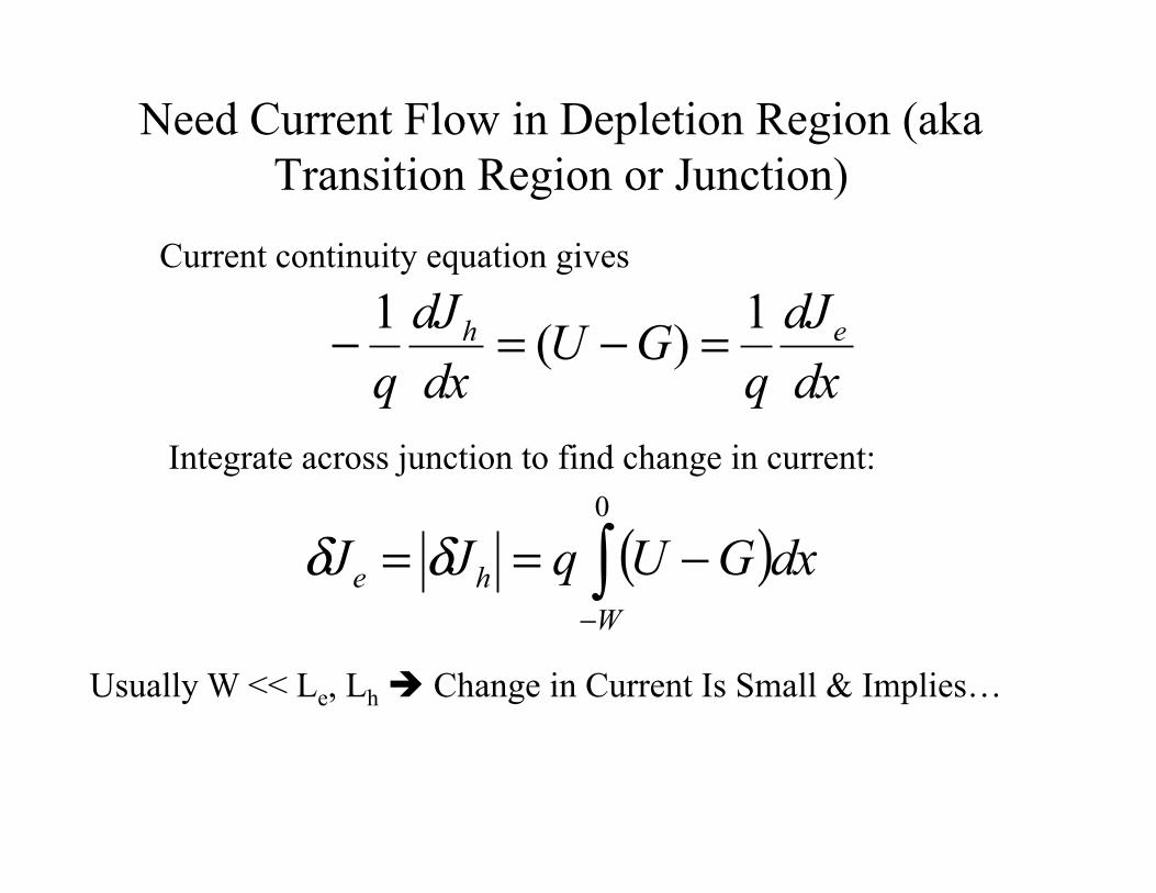
Need Current Flow in Depletion Region (aka Transition Region or Junction)
Current continuity equation gives
dxdJ
qGU
dxdJ
qeh 1)(1 =−=−
Integrate across junction to find change in current:
( )∫−
−==0
Whe dxGUqJJ δδ
Usually W << Le, Lh è Change in Current Is Small & Implies…

IF G=0…. Current Across Junction is ~Constant & Current Distribution Looks Like:
Constant Current Across
Junction

How to Find Majority Current in Quasineutral Region ?
Don’t Know Current Here

Q: How to Find Majority Current in Quasineutral Region ?
A: We Know Jtotal = Constant…
So Use Our Other Solutions (Jminority ~ exp(-x/L)
To Find
( )1)/exp(00 −⎟⎟⎠
⎞⎜⎜⎝
⎛+=+= kTqV
LpqD
LnqD
JJJh
nh
e
pehetotal

WE FOUND WHAT WE SEEK: J=J(V)
( )1)/exp(00 −⎟⎟⎠
⎞⎜⎜⎝
⎛+=+= kTqV
LpqD
LnqD
JJJh
nh
e
pehetotal
Current Density vs Voltage Across Diode:
Total Current, I (Amps), Is Just Jtotal * Area of Diode…
( )1)/exp()( 0 −= kTqVIVI
⎟⎟⎠
⎞⎜⎜⎝
⎛+=
h
nh
e
pe
LpqD
LnqD
AI 000

I-V Characteristics of p-n diode