Quad NTSC/PAL Decoder and Quad Audio Codec General ... · Quad NTSC/PAL Decoder and Quad Audio...
83
MAX9530 Quad NTSC/PAL Decoder and Quad Audio Codec _____________ General Description The MAX9530 is a quad-channel video decoder and audio codec for security & surveillance applications. The part is specially designed to serve as the front-end in multi-channel DVR (Digital Video Recorder) and DVS (Digital Video Streamer) systems. The architecture supports byte- or frame-interleaved digital video output for direct connection to a wide selection of multi-channel A/V media processors including Maxim’s own H.264 codec family (i.e. MG3500 and later generations). The on-chip DDR2 memory controller enables output of frame-synchronized digital video from up to four asynchronous analog video inputs. Multiple devices can be configured to support an unlimited number of synchronized video streams. The use of external memory is optional. A memory bypass mode provides for output of up to four-channels of asynchronous video data in BT.656 digital component format. The video signal path produces excellent video quality derived from four 54MHz/10-bit ADCs and a 5L comb filter bank. Differential or single-ended video and audio inputs are supported. The video input path includes a DC restore circuit, analog gain control, and anti-aliasing filter for each channel with no additional external components. Long cable connections are supported with the use of an adaptive equalizer block that automatically adjusts and compensates for high-frequency video signal losses in each channel independently. Each video channel can also be downscaled in high-quality for recording in lower resolution formats. All video capture operates from a unique “PLL-less” design, to ensure instant lock, and no loss of video content waiting for lock to occur with the incoming video. In addition, four mono audio channels are captured in 16-bit precision with programmable sample rates from 16 to 48kHz. Three independent I2S interfaces provide digital audio input/output for record, playback, and mixing operations. A separate inter-chip Audio Link bus allows cascaded operation for multi-channel systems with 8/16/etc. channel inputs. Two analog audio outputs are also provided. The digital I/Os can operate from 1.7 to 3.6V. ___________________Applications Security Surveillance/CCTV Systems Digital Video Recorders (DVRs) Digital Video Streamers (IP Streaming) ______________________ Features Video Features: 4-ch Analog Video Decoder – NTSC (M,J,4.43) or PAL(B,G,H,I,D,N,M,60) 4-ch Frame-Interleaved Output Synchronizer (optional with external DDR2 memory). Programmable 2D Video Scalers Independent Auto Cable EQ per Video Channel Instant Lock System for Video Capture Multi-Line Adaptive Comb Filters. 4x Oversampled 54MHz/10-bit Video ADC Output formats – Video - 4x8-bit non-interleaved or 2x2x8-bit / 1x4x8-bit interleaved DVR Multiplex Output: With DDR2 – Pixel or Frame Interleaved Without DDR2 – BT.656 Pixel Multiplex Audio Features: 4-ch Analog Audio Input (Mono) 48KHz/16 bit Audio ADC. 2-ch Analog Audio Output Differential or Single-Ended Analog Inputs I 2 C Interface 1400mW Typical Power Dissipation (w. DDR) 1.8V Analog Supply Voltage 1.8V Digital Core Supply Voltage 1.8V to 3.3V Digital I/O Voltage JTAG Support ____________Ordering Information PART INPUTS PIN-PACKAGE MAX9530CXV+ 4 + 4 CSBGA 196 All devices specified over the 0ºC to +70ºC operating temperature range. + Denotes lead(Pb)-free/RoHS-compliant package. Page 1 of 83
Transcript of Quad NTSC/PAL Decoder and Quad Audio Codec General ... · Quad NTSC/PAL Decoder and Quad Audio...
MAX9530 Quad NTSC/PAL Decoder and Quad Audio Codec
_____________ General Description The MAX9530 is a quad-channel video decoder and audio codec for security & surveillance applications. The part is specially designed to serve as the front-end in multi-channel DVR (Digital Video Recorder) and DVS (Digital Video Streamer) systems. The architecture supports byte- or frame-interleaved digital video output for direct connection to a wide selection of multi-channel A/V media processors including Maxim’s own H.264 codec family (i.e. MG3500 and later generations). The on-chip DDR2 memory controller enables output of frame-synchronized digital video from up to four asynchronous analog video inputs. Multiple devices can be configured to support an unlimited number of synchronized video streams. The use of external memory is optional. A memory bypass mode provides for output of up to four-channels of asynchronous video data in BT.656 digital component format. The video signal path produces excellent video quality derived from four 54MHz/10-bit ADCs and a 5L comb filter bank. Differential or single-ended video and audio inputs are supported. The video input path includes a DC restore circuit, analog gain control, and anti-aliasing filter for each channel with no additional external components. Long cable connections are supported with the use of an adaptive equalizer block that automatically adjusts and compensates for high-frequency video signal losses in each channel independently. Each video channel can also be downscaled in high-quality for recording in lower resolution formats. All video capture operates from a unique “PLL-less” design, to ensure instant lock, and no loss of video content waiting for lock to occur with the incoming video. In addition, four mono audio channels are captured in 16-bit precision with programmable sample rates from 16 to 48kHz. Three independent I2S interfaces provide digital audio input/output for record, playback, and mixing operations. A separate inter-chip Audio Link bus allows cascaded operation for multi-channel systems with 8/16/etc. channel inputs. Two analog audio outputs are also provided. The digital I/Os can operate from 1.7 to 3.6V.
___________________Applications Security Surveillance/CCTV Systems
Digital Video Recorders (DVRs) Digital Video Streamers (IP Streaming)
______________________ Features Video Features: 4-ch Analog Video Decoder – NTSC (M,J,4.43) or
PAL(B,G,H,I,D,N,M,60) 4-ch Frame-Interleaved Output Synchronizer
(optional with external DDR2 memory). Programmable 2D Video Scalers Independent Auto Cable EQ per Video Channel Instant Lock System for Video Capture Multi-Line Adaptive Comb Filters. 4x Oversampled 54MHz/10-bit Video ADC Output formats –
Video - 4x8-bit non-interleaved or 2x2x8-bit / 1x4x8-bit interleaved
DVR Multiplex Output: With DDR2 – Pixel or Frame Interleaved Without DDR2 – BT.656 Pixel Multiplex
Audio Features: 4-ch Analog Audio Input (Mono) 48KHz/16 bit Audio ADC. 2-ch Analog Audio Output Differential or Single-Ended Analog Inputs I2C Interface 1400mW Typical Power Dissipation (w. DDR) 1.8V Analog Supply Voltage 1.8V Digital Core Supply Voltage 1.8V to 3.3V Digital I/O Voltage JTAG Support
____________Ordering Information
PART INPUTS PIN-PACKAGE MAX9530CXV+ 4 + 4 CSBGA 196
All devices specified over the 0ºC to +70ºC operating temperature range. + Denotes lead(Pb)-free/RoHS-compliant package.
Page 1 of 83
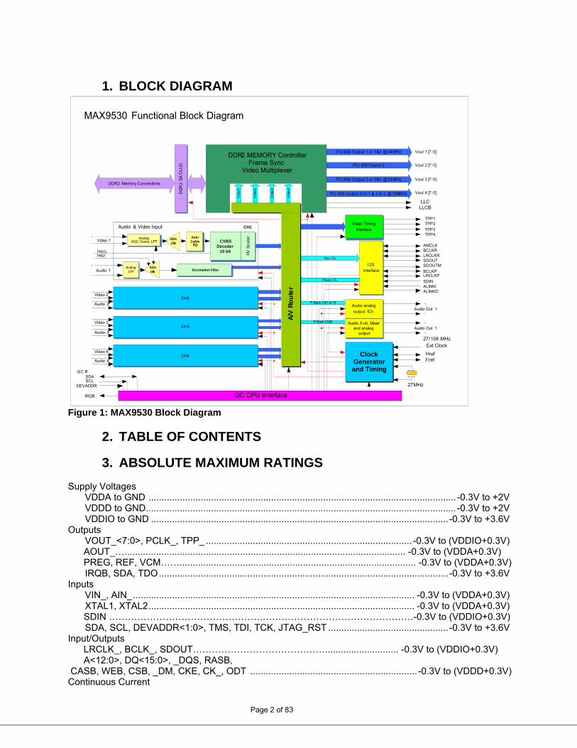
1. BLOCK DIAGRAM
Audio 4
Video 4
Audio 3
Video 3
Audio 2
Video 2
Audio 1
MAX9530 Functional Block Diagram
CVBSDecoder
10 bit
ADC10b
ADC16b Decimation Filter
Audio & Video Input CH1
I2C CPU Interface
ClockGeneratorand Timing
27/108 MHzExt Clock
Vout 1 [7:0]
Analog:AGC, Clamp, LPF
AnalogLPF
I2C IF
ITU 656 Output 1 or 1&2 @ 54MHz
AutoCable
EQ
ITU 656Output 2
ITU 656 Output 3 or 3&4 @ 54MHz
ITU 656 Output 4 or 1 & 2 & 4 @ 108MHz
Vout 2 [7:0]
Vout 3 [7:0]
Vout 4 [7:0]
Video Timing
Interface
TPP1TPP2
TPP3TPP4
LLCBLLC
SDASCL
IRQB
I2SInterface
AMCLKBCLKRLRCLKRSDOUTSDOUTM
BCLKPLRCLKPSDINALINKIALINKO
Audio Out 1
HV
Sc
ala
r
27MHz
Video 1
DD
R2
DA
TA
I/O
DDR2 Memory Connections
Audio analog
output 1Ch.Audio Out 1
Audio 5 ch. Mixerand analog
output
DDR2 MEMORY ControllerFrame Sync
Video Multiplexer
Vid
eo1
Vid
eo2
Vid
eo3
Vid
eo4
Rec. Ch
P.back Ch.
P. Back Ch[5]
P.Back Ch[1 of 5]
A/V
Ro
ute
r
HrefFref
CH4
CH3
CH2
DEVADDR
PREGPREF
Figure 1: MAX9530 Block Diagram
2. TABLE OF CONTENTS
3. ABSOLUTE MAXIMUM RATINGS Supply Voltages VDDA to GND ...................................................................................................................... -0.3V to +2V VDDD to GND....................................................................................................................... -0.3V to +2V VDDIO to GND ..................................................................................................................-0.3V to +3.6V Outputs VOUT_<7:0>, PCLK_, TPP_ ............................................................................... -0.3V to (VDDIO+0.3V) AOUT_…........................................................................................................... -0.3V to (VDDA+0.3V) PREG, REF, VCM…….......................................................................................... -0.3V to (VDDA+0.3V) IRQB, SDA, TDO............................................................................................................... -0.3V to +3.6V Inputs VIN_, AIN_............................................................................................................ -0.3V to (VDDA+0.3V) XTAL1, XTAL2...................................................................................................... -0.3V to (VDDA+0.3V) SDIN ………………………………………….…………………………………………-0.3V to (VDDIO+0.3V) SDA, SCL, DEVADDR<1:0>, TMS, TDI, TCK, JTAG_RST .............................................. -0.3V to +3.6V Input/Outputs LRCLK_, BCLK_, SDOUT……………………………………............................ -0.3V to (VDDIO+0.3V) A<12:0>, DQ<15:0>, _DQS, RASB, CASB, WEB, CSB, _DM, CKE, CK_, ODT ................................................................ -0.3V to (VDDD+0.3V)
Page 2 of 83
Continuous Current
All Pins........................................................................................................................................ +/-50mA Continuous Power Dissipation (TA = +70ºC) 196 pin CSBGA Multilayer Board (derate 20.8mW/C above +70C) …………………………………………………………………………1860mW Operating Temperature Range ................................................................................................. 0ºC to +70ºC Junction Temperature ........................................................................................................................ +150ºC Storage Temperature Range ................................................................................................-65ºC to +150ºC Lead Temperature (soldering, 10sec)................................................................................................. +260ºC Note A: Package thermal resistances were obtained using the method described in JEDEC specification JESD51-7, using a 4-layer board. For detailed information on package thermal considerations see www.maxim-ic.com/thermal-tutorial Stresses beyond those listed under “Absolute Maximum Ratings” may cause permanent damage to the device. These are stress ratings only and functional operation of the device at these or any other conditions beyond those indicated in the operational sections of the specifications are not implied. Exposure to absolute maximum rating conditions for extended periods may affect device reliability.
4. ELECTRICAL CHARACTERISTICS: EC TABLE (VDDA = VDDD = +1.8V, VDDIO = +3.3V, GND = 0V, TA = 0°C to 70°C, unless otherwise noted. Typical values are at TA = +25°C.) (Note 1)
EC Table PARAMETER SYMBOL CONDITIONS MIN TYP MAX
UNITS
SUPPLIES Analog Supply Voltage Range VDDA 1.7 1.8 1.9 V Digital Supply Voltage Range VDDD 1.7 1.8 1.9 V Digital I/O Supply Voltage Range VDDIO 1.7 3.3 3.45 V
Normal Operation (Note 2) 152 250 mA Analog Supply Current IVDDA
Shutdown (XTAL=0Hz) 2 200 µA Normal Operation (Note 2) 344 490 mA Digital Supply Current
IVDDD Shutdown (XTAL=0Hz) 50 1000 µA
Normal Operation (Note 2). VDDIO=1.8V 52 mA
Normal Operation (Note 2). VDDIO=3.3V 150 mA
Digital I/O Supply Current
IVDDIO
= 25°C) Shutdown. DVDD_IO=3.3V (TA 10 µA
ANALOG VIDEO INPUT Video Input Reference (VREF) VREF 775 mV Video Input Resistance RIN 2 MΩ Video Input Capacitance CIN 8 pF Diff. Video Input CMRR CMRRv Freq. range 0 5MHz 80 dBFS
Slow 2.1 3 3.9 Medium 4.2 6 7.8 Medium-Fast (default) 8 12 16
Video Sync Level Adjust (Source and Sink Values) (Note 6) DC Restore Current DAC Full Scale Range (Source and Sink)
Fast
Page 3 of 83
16.4 24 32
µA
ANALOG INPUT FILTER AND ADC (Note 4) Video Passband Cutoff (3dB) F3dB 13 MHz
Video Passband Flatness f < FPB, VAIN = 0.65VP-P reference level is measured at 1MHz
0.25 dB
Video Stopband Cutoff FSB 53 MHz
Video Stopband Attenuation f > FSB, VAIN = 0.65VP-P reference level is measured at 1MHz 36 dB
EC Table PARAMETER SYMBOL CONDITIONS MIN TYP MAX
UNITS
ADCGAIN=0x0 680 840 mVpp Video Full-Scale Conversion Single End Input
AGC Disabled, Gain Programmed
via I2C,Referenced to VINxN, Gain Error=5% ADCGAIN=0xF 280 340 mVpp
ADCGAIN=0x0 1370 1690 mVpp Video Full-Scale Conversion Differential Input
AGC Disabled, Gain Programmed via I2C, Referenced to VINxN, Gain Error=5% ADCGAIN=0xF 550 670 mVpp
Video AGC Step Size 0.150 V/V ADC Clock Rate Fadc 54 MHz ADC Resolution ADCR 10 Bits Video DC differential nonlinearity DNL ±0.5 LSB Video DC integral nonlinearity INL ±1 LSB Video Signal-to-RMS noise ratio (Includes filter + ADC + digital anti-aliasing filter)
SNR Luminance Flat Field -50% gray 56 dB
Video Power Supply Rejection PSRV Av=0000, ADCGAIN[3:0]=0x0 TA = +25°C
1.7V<VVDDA<1.9V 1.7V<VVDDD<1.9V 1.7V<VVDDIO<3.45V
33 dBFS
Video Differential Phase DP 5 step Modulated Staircase, f =3.58MHz or 4.43MHz
1.0 Deg.
Video Differential Gain DG 5 step Modulated Staircase, f =3.58MHz or 4.43MHz 1 %
Video 2T Pulse Response 2T = 200ns 2T = 250ns 0.2 K%
Between video channels 70 Crosstalk
Between audio input channels 90 dB
DECODED LUMINANCE and CHROMINANCE Video Chrominance Bandwidth BWC 1.0 MHz Video Luminance Bandwidth BWL 5.5 MHz Video Luminance Non-Linearity 5-step staircase 1.0 % Chroma Amplitude error 1 % Chroma Phase Error +/- 1 deg Video Horizontal Line Time Static Variation 1.5 % Video Maximum Horizontal Line Time Jitter 8 µs
B&W Signal 12 Video Input Signal Minimum Peak Signal to RMS Noise
Proper composite decoder operation Color Signal
Page 4 of 83
18 dB
CLOCK GENERATOR Video Clock Jitter 400 psp-p CRYSTAL OSCILLATOR (XTAL1, XTAL2) Frequency Fundamental Mode Only 27.0000 MHz
XTAL1, XTAL2 Input Capacitance CXTAL1, CXTAL2
4 pF
Maximum Load Capacitor CL1, CL2 45 pF Frequency Accuracy ±50 ppm Maximum Input Clock Jitter External Clock 600 pspp
I²C SERIAL INTERFACE (SDA, SCL) Serial Clock Frequency fSCL 0 400 kHz Bus Free Time Between STOP and START Conditions
tBUF 1.3 µs
EC Table PARAMETER SYMBOL CONDITIONS MIN TYP MAX
UNITS
Hold Time (repeated) START Condition. tHD,STA 0.6 µs SCL Pulse Width Low tLOW 1.3 µs SCL Pulse Width High tHIGH 0.6 µs Setup Time for a Repeated START Condition
tSU,STA 0.6 µs
Data Hold Time tHD,DAT 0 900 ns Data Setup Time tSU,DAT 100 ns SDA and SCL Receiving Rise Time tr Note 3 20+0.1CB 300 ns SDA and SCL Receiving Fall Time tf Note 3 20+0.1CB 300 ns SDA Transmitting Fall Time tf 20+0.1CB 500 ns Setup Time for STOP Condition tSU,STO 0.6 µs Bus Capacitance CB 400 pF Pulse Width of Suppressed Spike tSP 0 50 ns HIGH-SPEED LOGIC OUTPUTS (VOUT_<7:0>, PCLK_, TPP_, BCLK_, LRCLK_, SDOUT_, SDIN, SDIO_AL) Output Low Voltage VOL IOL = 2mA, ODS = 01 0.4 V Output High Voltage
VOH IOH = 2mA, ODS = 01 VDDIO –
0.4V V
VID_<7:0> to PCLK27, ODS = 01 32.41 VID_<7:0> to PCLK54, ODS = 01 13.89
Data to Clock Rising Edge Hold Time tHD
VID_<7:0> to PCLK108, ODS = 01 4.63 ns
VID_<7:0> to PCLK27, ODS = 01 4.63 VID_<7:0> to PCLK54, ODS = 01 4.63
Data to Clock Rising Edge Setup Time tSU
VID_<7:0> to PCLK108, ODS = 01 4.63 ns
CL=10pF, DVDD_IO=1.8V 3 Rise and Fall Time (20% to 80%)
Tr, Tf =25pF, DVDD_IO=3.3V CL 3
ns
Output Leakage IOH, IOL Outputs in High-Z Mode -3 ±0.01 3 µA OPEN-DRAIN LOGIC OUTPUT (SDA)
IOL = 3mA, VDDIO = 1.8V 0.2 x VDDIO
Output Low Voltage VOL
I = 3mA, VDDIO = 3.3V OL 0.4
V
Output High Current IOH VOUT = 3.3V ±0.01 3 µA LOGIC INPUTS (SDA, SCL, DEVADDR <1:0>, BCLK, LRCLK, SDIN, SDIO, FREF, HREF, TCK, TMI, TDS, JTAGRST, REF27I ) Logic Low Threshold VIL 0.3 x
DVDD_IO V
Logic High Threshold VIH 0.7 x VDDIO V
Input Leakage Current I IH, I IL (TA = 25°C) -3 ±0.01 3 µA SDA/SCL Off Leakage IIHI2C VDDA=VDDD=VDDIO=0V, SDA=SCL=3.6V -3 ±0.01 3 µA AUDIO LINE OUT
Single ended output -10 ±1 10 Audio Output Gain Error AOGE
Differential output -10 ±1 10 %
0dB gain, single ended output 1 Audio Output Full Scale AOFS
0dB gain, differential output 2 Vpp
Single ended output, Fs = 48kHz 80 90 Audio Output Dynamic Range DR
Differential output, Fs = 48kHz 80 90 dB
Audio Output THD+N THDN Differential output, Fs = 48kHz 66 75 dB 1.7V<VVDDA<1.9V, 1.7V<VVDDD<1.9V, 1.7V<VVDDIO<3.45V, single ended output 74 [80] Audio Output Power Supply Rejection
Ratio PSRA 1.7V<V <1.9V, 1.7V<V <1.9V, VDDA VDDD
1.7V<V <3.45V, differential output VDDIO 74 [80]
dB
Audio Output Capacitive Drive RL=10kΩ, no sustained oscillations 100 pF AUDIO DAC HIGHPASS DIGITAL FILTER
DACxHPF = 00 200 Audio Output Cutoff Frequency fDHPPB DACxHPF = 01
Page 5 of 83
100 Hz
EC Table PARAMETER SYMBOL CONDITIONS MIN TYP MAX
UNITS
DACxHPF = 10 50 DACxHPF = 11 disabled
AUDIO LINE IN Single ended input -10 ±1 10
Audio Input Gain Error AIGE Differential input -10 ±1 10
%
Single ended Input 1.4 Audio Input Full Scale AIFS
Differential Input 2.8 Vpp
Single ended input, Fs = 48kHz 66 80 Audio Input Dynamic Range DR
Differential input, Fs = 48 kHz 66.9 81 dB
Audio Input THD+N THD+N Differential input, Fs = 48kHz 58 69 dB Audio Input Gain GAIN Differential input, ADCLEV from 0000 to 1111 -12 +3 dB Diff. Input CMRR CMRRa Freq. Range 0 20KHz 90 dBFS
1.7V<VVDDA<1.9V, 1.7V<VVDDD<1.9V, 1.7V<VVDDIO<3.45V, input referred, single ended input
70 Audio Input Power Supply Rejection Ratio
PSRD <1.9V, 1.7V<V <1.9V, 1.7V<VVDDA VDDD
1.7V<VVDDIO<3.45V, input referred, differential input
70
dB
1kHz, 0dBFS, single ended input -80 Audio Input Total Harmonic Distortion THD
1kHz, 0dBFS, differential input -80 dB
1kHz 0dBFS, single ended input 83 Audio Input Signal to Noise Ratio SNR
1kHz 0dBFS, differential input 83 dB
Single-ended input 35 Audio Input Resistance RINA Differential input 35
kΩ
AUDIO ADC DIGITAL HIGHPASS FILTER ADCHPF = 00 200 ADCHPF = 01 100 ADCHPF = 10 50
Audio Input Cutoff Frequency fAHPSB
ADCHPF = 11 disabled
Hz
DDR2 Interface (_DQS,DQ<15:0>,_DM, WEB, RASB, CASB, ODT, CKE, CK_, CSB, A<12:0>) Note 7 Memory Clock Period tCK 6.2 ns SSTL18 Reference Voltage VrefDC 0.5*VDDD V
TA = +25°C VrefDC +125 SSTL18 Input High VihDC
= 0°C to 70°C TA VrefDC +200
mV
TA = +25°C VrefDC –125
SSTL18 Input Low VilDC
= 0°C to 70°C TA
VrefDC –250
mV
SSTL18 Output High VOHDDR2 Load = 13.4mA; VDDD=1.7V 1.2 1.5 V SSTL18 Output Low VOLDDR2 Load = 13.4mA; VDDD=1.7V 0.18 0.3 V SSTL18 Input cross-point VIXDDR2 Differential inputs VrefDC mV SSTL18 Output cross-point VOXDDR2 Differential outputs VrefDC mV SSTL18 CM Output Voltage VCMDDR2 Differential outputs, differential termination VrefDC mV SSTL18 Output slew rate OSDDR2 3 V/ns DQS/DQ write skew tDDR2DLY Write mode (DQS/DQ are outputs) 1.55 ns
Table 1: EC Table Note 1: All devices are 100% production tested at TA=+25ºC. Specifications over temperature limits are guaranteed by design. Note 2: NTSC 75% Color Bar signal applied to analog input. CL = 10pF on logic output pins (D7-D0 and PCLK27). Note 3: CB is in pF. Note 4: Filter and ADC performance measured using ADC outputs prior to composite digital demodulation (decoding). Note 5: Decoded Luminance and Chrominance specifications measured using entire signal path from analog input to digital component
outputs.
Page 6 of 83
Note 6: Internal test only. Digital core controls sync level adjust current to adjust offset in analog signal path. Adjust level is based on value of sync level as converted by ADC. Digital core switches sourcing or sinking current into AIN1 and AIN2 nodes. Speed of correction (value of current) is controlled through I2C.
Note 7: SSTL18 differential signals are UDQS/B, LDQS/B, and CK/B. All others are single ended. See reference JEDEC Std. 8-15A for detailed test information.
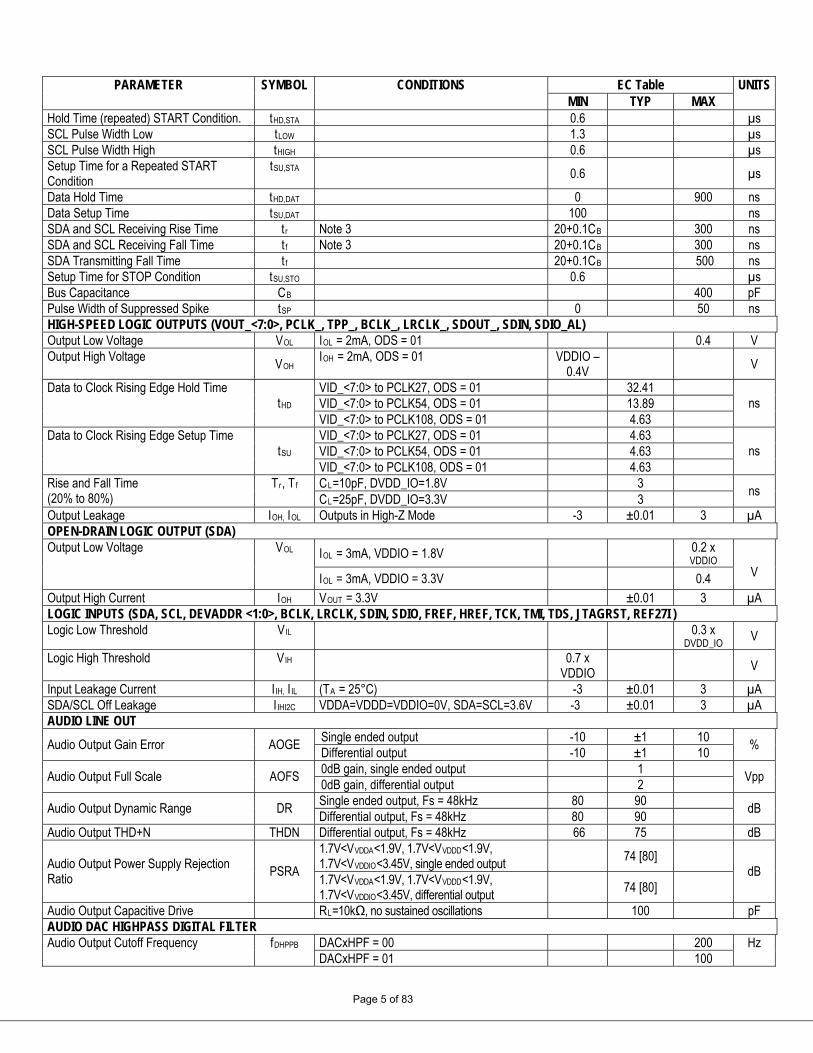
5. Typical Operating Characteristics (VAVDD = VDVDD = +1.8V, VDVDDIO = 3.3V, VAGND = VDGND = 0V, TA = TMIN to TMAX, unless otherwise noted. Typical values are at TA = +25°C.) VIDEO ADC FULL-SCALE CONVERSION RANGE GAIN CODE (Reg0x0A[3:0]) (DECIMAL) / FULL-SCALE INPUT RANGE (mVP-P)
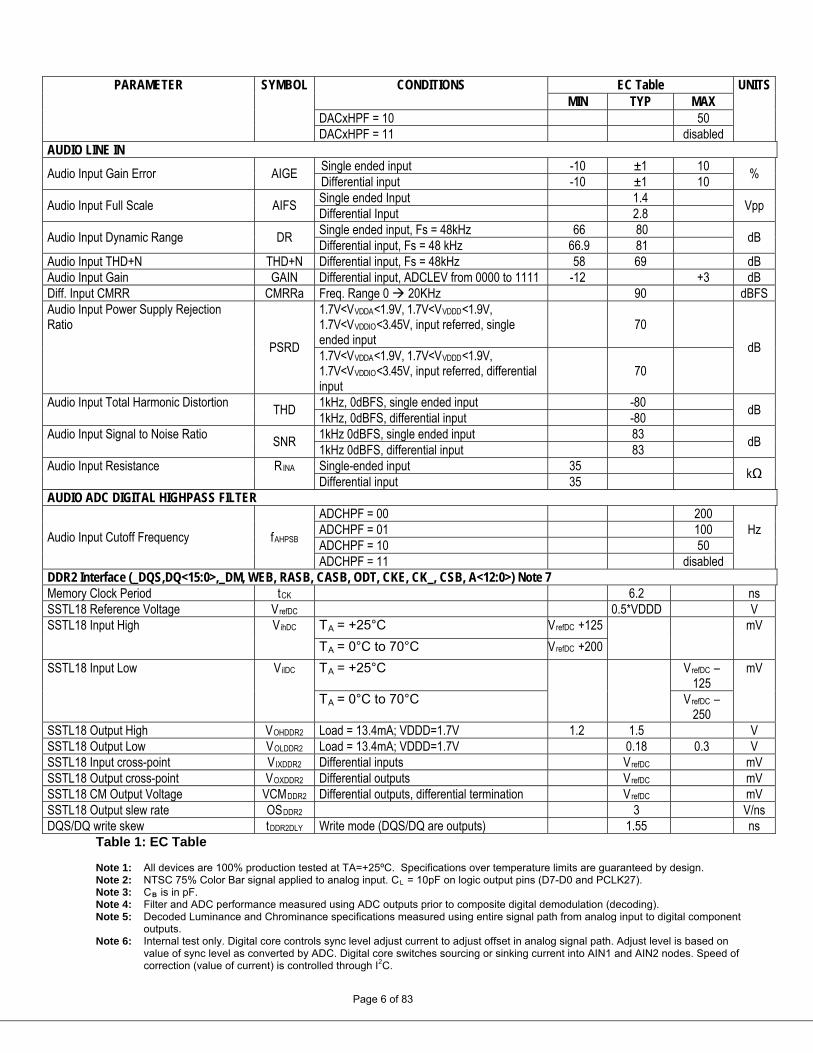
Figure 2: VIDEO ANALOG AGC RANGE VIDEO ANALOG INPUT FILTER RESPONSE FREQUENCY (MHz) / AMPLITUDE (dB)
Page 7 of 83
Figure 3: VIDEO ANALOG INPUT FILTER RESPONSE
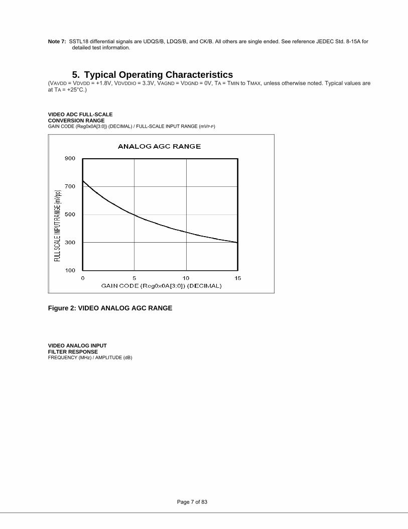
VIDEO DIGITAL COMPOSITE ANTI-ALIASING FILTER FREQUENCY (MHz) / AMPLITUDE (dB)
Figure 4: VIDEO DIGITAL COMPOSITE ANTI-ALIASING FILTER VIDEO DIGITAL Y FILTER FREQUENCY (MHz) / AMPLITUDE (dB)
Page 8 of 83
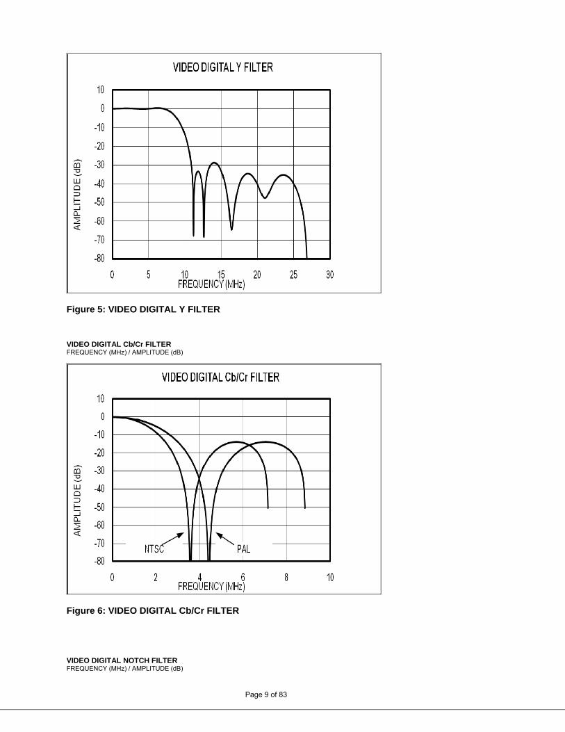
Figure 5: VIDEO DIGITAL Y FILTER
VIDEO DIGITAL Cb/Cr FILTER FREQUENCY (MHz) / AMPLITUDE (dB)
Figure 6: VIDEO DIGITAL Cb/Cr FILTER
VIDEO DIGITAL NOTCH FILTER
Page 9 of 83
FREQUENCY (MHz) / AMPLITUDE (dB)
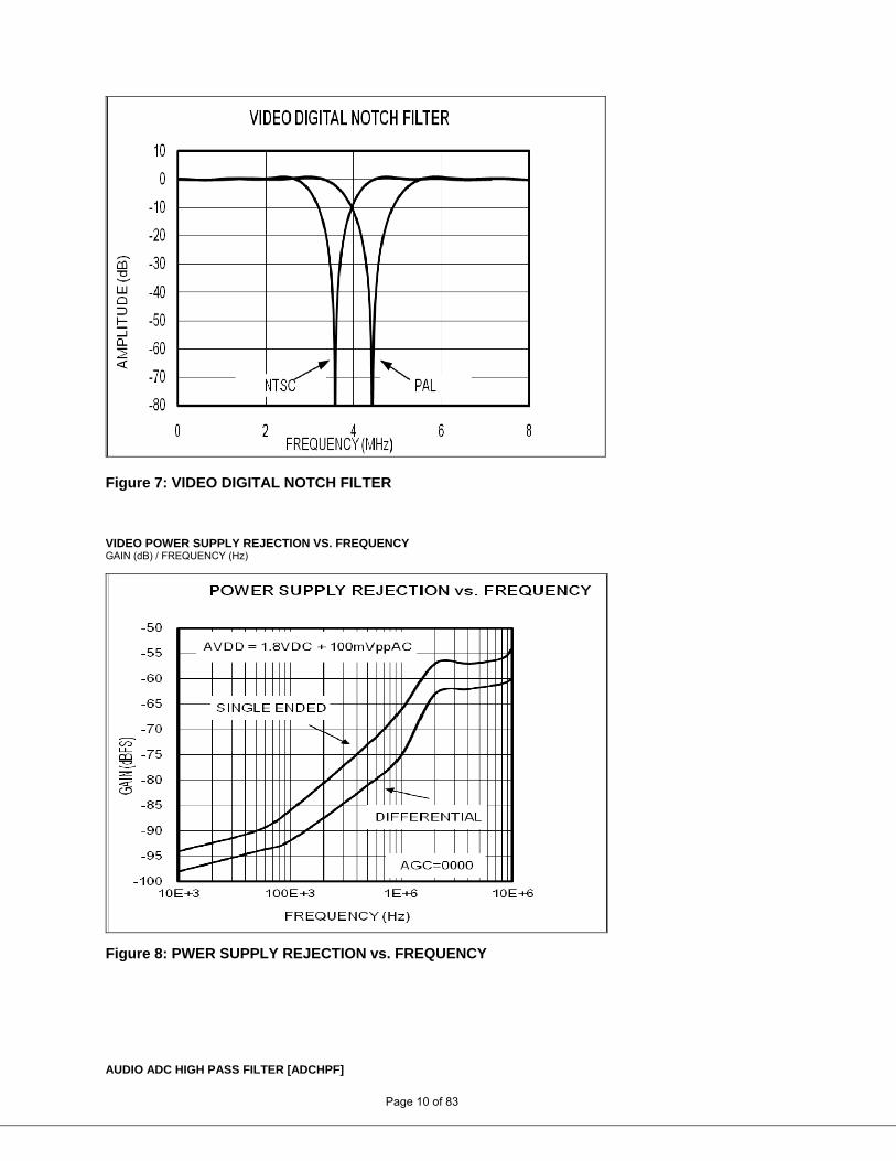
Figure 7: VIDEO DIGITAL NOTCH FILTER
VIDEO POWER SUPPLY REJECTION VS. FREQUENCY GAIN (dB) / FREQUENCY (Hz)
Figure 8: PWER SUPPLY REJECTION vs. FREQUENCY
A
Page 10 of 83
UDIO ADC HIGH PASS FILTER [ADCHPF]
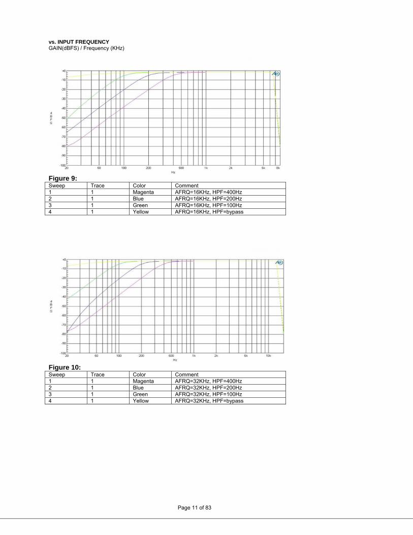
vs. INPUT FREQUENCY GAIN(dBFS) / Frequency (KHz)
Figure 9:Sweep
Trace Color Comment
1 1 Magenta Hz, HPF=400Hz AFRQ=16K2 1 Blue AFRQ=16KHz, HPF=200Hz 3 1 Green AFRQ=16KHz, HPF=100Hz 4 1 Yellow AFRQ=16KHz, HPF=bypass
Figure 10:Sweep
Trace Color Comment
1 1 Magenta Hz, HPF=400Hz AFRQ=32K2 1 Blue AFRQ=32KHz, HPF=200Hz 3 1 Green AFRQ=32KHz, HPF=100Hz 4 1 Yellow AFRQ=32KHz, HPF=bypass
Page 11 of 83
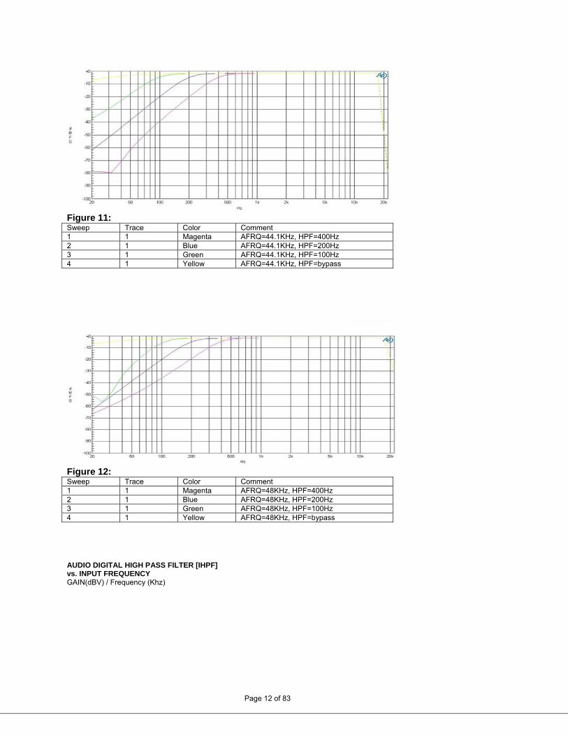
Figure 11: Sweep Trace Color Comment 1 1 Magenta AFRQ=44.1KHz, HPF=400Hz 2 1 Blue AFRQ=44.1KHz, HPF=200Hz 3 1 Green AFRQ=44.1KHz, HPF=100Hz 4 1 Yellow AFRQ=44.1KHz, HPF=bypass
Figure 12: Sweep Trace Color Comment 1 1 Magenta AFRQ=48KHz, HPF=400Hz 2 1 Blue AFRQ=48KHz, HPF=200Hz 3 1 Green AFRQ=48KHz, HPF=100Hz 4 1 Yellow AFRQ=48KHz, HPF=bypass
AUDIO DIGITAL HIGH PASS FILTER [IHPF] vs. INPUT FREQUENCY GAIN(dBV) / Frequency (Khz)
Page 12 of 83
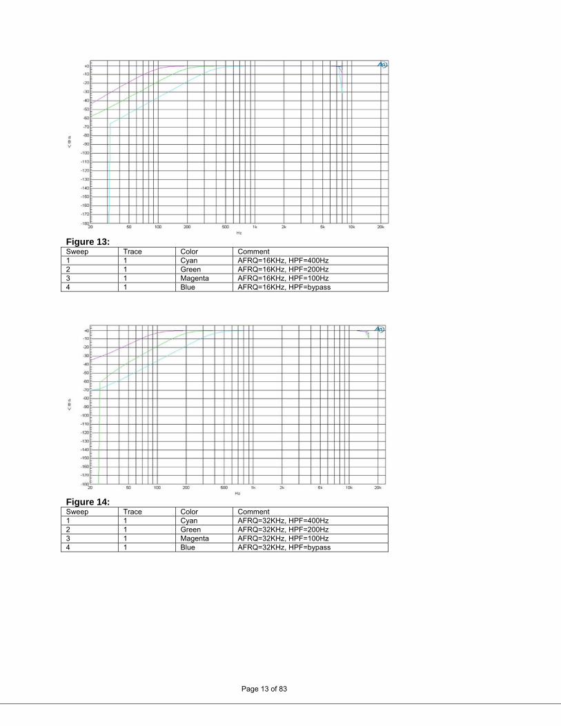
Figure 13: Sweep Trace Color Comment 1 1 Cyan AFRQ=16KHz, HPF=400Hz 2 1 Green AFRQ=16KHz, HPF=200Hz 3 1 Magenta AFRQ=16KHz, HPF=100Hz 4 1 Blue AFRQ=16KHz, HPF=bypass
Figure 14: Sweep Trace Color Comment 1 1 Cyan AFRQ=32KHz, HPF=400Hz 2 1 Green AFRQ=32KHz, HPF=200Hz 3 1 Magenta AFRQ=32KHz, HPF=100Hz 4 1 Blue AFRQ=32KHz, HPF=bypass
Page 13 of 83
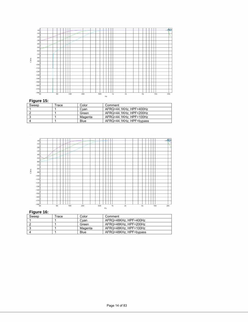
Figure 15: Sweep Trace Color Comment 1 1 Cyan AFRQ=44.1KHz, HPF=400Hz 2 1 Green AFRQ=44.1KHz, HPF=200Hz 3 1 Magenta AFRQ=44.1KHz, HPF=100Hz 4 1 Blue AFRQ=44.1KHz, HPF=bypass
Figure 16: Sweep Trace Color Comment 1 1 Cyan AFRQ=48KHz, HPF=400Hz 2 1 Green AFRQ=48KHz, HPF=200Hz 3 1 Magenta AFRQ=48KHz, HPF=100Hz 4 1 Blue AFRQ=48KHz, HPF=bypass
Page 14 of 83
6. Pin Configuration
Top View (Through Package)
L R
1 2 3 4 5 6 7 8 9 10 11 12 13 14
A SDIOA L
BCLK P
BCLK R
PCLK 108
PCLK 27
TPP1 VOUT 37
VOUT 36
VOUT 35
VOUT 34
VOUT 17
VOUT 16
VOUT 15
VOUT 14
B BCLKA L
LRCLK P
LRCLK R
PCLK 108B
PCLK 27B
TPP2 VOUT 33
VOUT 32
VOUT 31
VOUT 30
VOUT 13
VOUT 12
VOUT 11
VOUT 10
C LRCLKAL
SDIN SDOUT HREF PCLK 54
TPP3 VOUT 47
VOUT 46
VOUT 45
VOUT 44
VOUT 27
VOUT 26
VOUT 25
VOUT 24
D XTAL 1
SDOUT M
MCLK R
FREF PCLK 54B
TPP4 VOUT 43
VOUT 42
VOUT 41
VOUT 40
VOUT 23
VOUT 22
VOUT 21
VOUT 20
E XTAL 2
REF 27O
REF 27I GND VDDA GND GND VDD VDD VDDIO A12 A11 A10 A9
F GND VIN1P VIN1N GND VDDA GND GND VDD VDD VDDIO A8 A7 A6 A5
G GND GND GND GND VDDA GND GND VDD VDD VDDIO A4 A3 A2 A1
H GND VIN2P VIN2N GND VDDA GND GND VDD VDD VDDIO A0 BA1 BA0 CSB
J GND GND GND GND VDDA GND GND VDD VDD VDDIO DQ15 DQ14 DQ13 DQ12
K GND VIN3P VIN3N GND VDDA GND GND VDD VDD VDDIO DQ11 DQ10 DQ9 DQ8
L GND GND GND AUD GND
PREF PREG TMS IRQB CKE RASB UDM UDQS UDQSB VREF
M GND VIN4P VIN4N VCM AOUT 2P
AOUT 2N
TCK SDA CK CASB DQ7 DQ6 DQ5 DQ4
N AIN1P AIN1N AIN2P AIN2N AOUT 1P
AOUT 1N
TDO SCL CKB WEB DQ3 DQ2 DQ1 DQ0
P AIN3P AIN3N AIN4P AIN4N GND JTAG RST
TDI DEV ADDR1
DEV ADDR0
RSTB LDM LDQS LDQSB ODT
Figure 17: MAX9530 pin configuration
Page 15 of 83

7. Pin Description Table 2:
Page 16 of 83
Ball Ball Name Type Pin Description Audio I/O
BCLKR A3 I/O Audio serial clock input/output of record. LRCLKR B3 I/O Audio serial sync input/output of record. MCLKR D3 O Audio master clock output of record. SDOUT C3 O Audio serial data output of record.
SDOUTM D2 O Audio serial data output of mixing. BCLKP A2 I/O Audio serial clock input/output of playback.
LRCLKP B2 I/O Audio serial sync input/output of playback. SDIN C2 I Audio serial data input of playback.
BCLKAL B1 I/O Audio Multi-chip operation serial bit clock I/O LRCLKAL C1 I/O Audio Multi-chip operation serial word clock I/O SDIOAL A1 I/O Audio Multi-chip operation serial input/output
AIN1P, AIN1N N1, N2 I Audio input of channel 1. AIN2P, AIN2N N3, N4 I Audio input of channel 2. AIN3P, AIN3N P1, P2 I Audio input of channel 3. AIN4P, AIN4N P3, P4 I Audio input of channel 4.
AUDGND L4 A Audio reference ground return.
AOUT1P,N N5, N6 O Analog audio output 1. AOUT2P,N M5, M6 O Analog audio output 2.
PREG L6 A Audio regulator output.
PREF L5 A Audio reference output.
VCM M4 A Audio common mode reference.
Video I/O VIN1P, VIN1N F2, F3 I Composite video input of channel 1. VIN2P, VIN2N H2, H3 I Composite video input of channel 2. VIN3P, VIN3N K2, K3 I Composite video input of channel 3. VIN4P, VIN4N M2, M3 I Composite video input of channel 4.
VOUT1[0:7] B14, B13, B12, B11, A14, A13, A12, A11
O Video data output of channel 1.
VOUT2[0:7] D14, D13, D12, D11, C14, C13, C12, C11
O Video data output of channel 2.
VOUT3[0:7] B10, B9, B8, B7, A10, A9, A8, A7
O Video data output of channel 3.
VOUT4[0:7] D10, D9, D8, D7, C10, C9, C8, C7
O Video data output of channel 4.
I2C Interface SDA M8 IO Serial control data line.
SCL N8 I Serial control clock line.
DEVADDR[1:0] P8, P9 I Serial control address.
JTAG JTAGRST P6 I Active low
TMS L7 I TCK M7 I 6MHz max TDO N7 O TDI P7 I
DDR2 Memory Interface CKE L9 O Clock enable
RASB, CASB, WEB
L10, M10, N10 O Command inputs
CK, CKB M9, N9 O CK and nCK are differential clock inputs.
162 MHz, differential 100 ohm
DQ[0:15]
N14, N13, N12, N11, M14, M13, M12,
M11, K14, K13, K12, K11, J14, J13, J12,
J11
I/O Data input/output - 50 Ohm
LDQS, LDQSB P12, P13 I/O Data strobe for lower byte
162 MHz, differential 100 ohm LDM, UDM P11, L11 O Input data mask
UDQS, UDQSB L12, L13 I/O Data strobe for upper byte
162 MHz, differential 100 ohm ODT P14 O On-die termination
CSB H14 O Chip select
VREF L14 I Vref BA0, BA1 H13, H12 O Bank address inputs
A[0:12]
H11, G14, G13, G12, G11, F14, F13, F12, F11, E14, E13, E12,
E11
O Address inputs
Timing/IRQ/Reset RSTB P10 I System reset.
IRQB L8
O Interrupt request output. This signal has positive logic and cannot be connected directly with other IRQs in the system. Pull-up resistor is still required.
XTAL1, XTAL2 D1, E1 I 27MHz Xtal or External 27 TPP1, TPP2, TPP3, TPP4
A6, B6, C6, D6 O
HS/VS/FLD/ACTIVE/NOVID of channel 1,2,3 & 4
PCLK27, PCLK27B
A5, B5 O 27 MHz clock output.
PCLK54, PCLK54B
C5, D5 O 54 MHz clock output.
PCLK108, PCLK108B
A4, B4 O 108 MHz clock output.
HREF, FREF C4, D4 IO External H and F Reference Input /Output
REF27O E2 O Reference Clock Output.
REF27I E3 I Reference Clock Input.
Power and Ground Pins VDDD P 1.8V Power for internal logic.
VDDIO P 3.3V Power for output driver.
GND G Global ground.
VDDA P 1.8V Power for analog audio.
Page 17 of 83
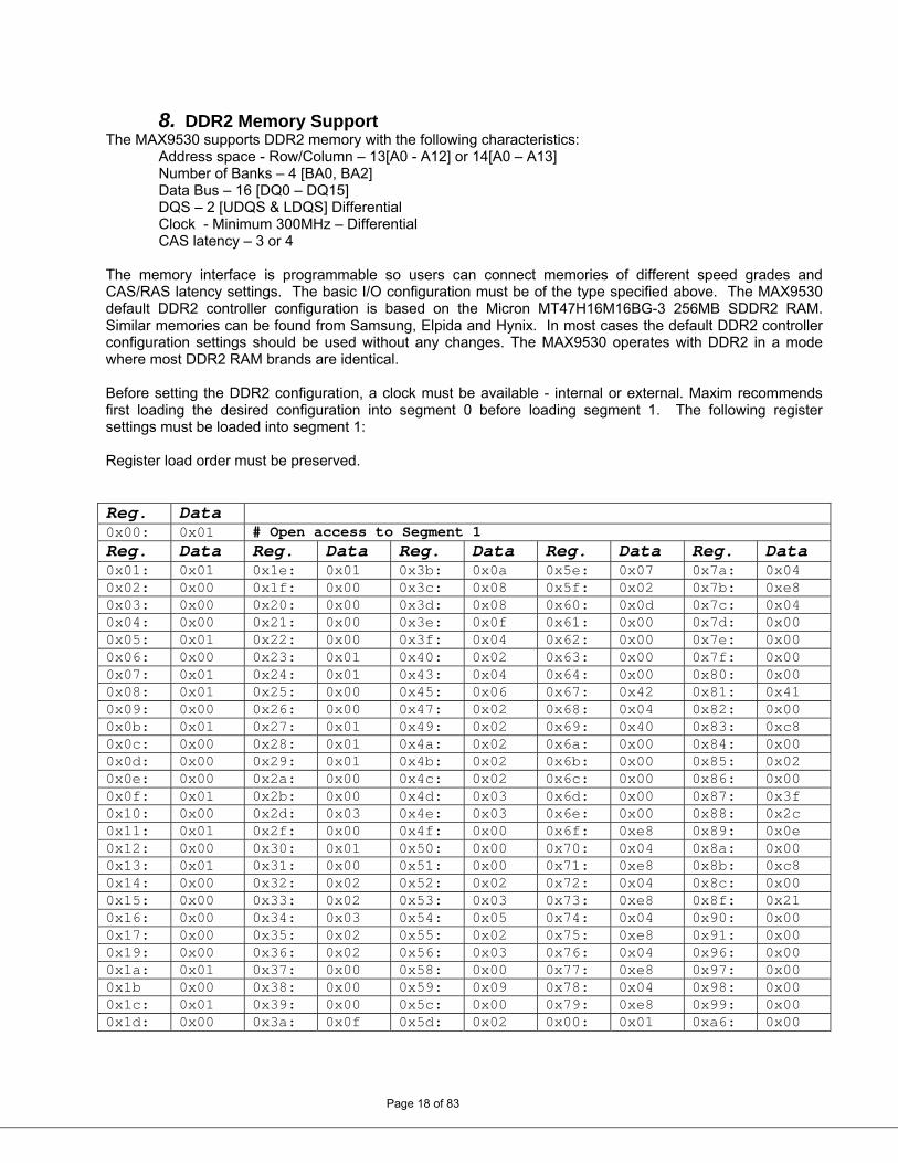
8. DDR2 Memory Support
The MAX9530 supports DDR2 memory with the following characteristics: Address space - Row/Column – 13[A0 - A12] or 14[A0 – A13] Number of Banks – 4 [BA0, BA2] Data Bus – 16 [DQ0 – DQ15] DQS – 2 [UDQS & LDQS] Differential Clock - Minimum 300MHz – Differential CAS latency – 3 or 4
The memory interface is programmable so users can connect memories of different speed grades and CAS/RAS latency settings. The basic I/O configuration must be of the type specified above. The MAX9530 default DDR2 controller configuration is based on the Micron MT47H16M16BG-3 256MB SDDR2 RAM. Similar memories can be found from Samsung, Elpida and Hynix. In most cases the default DDR2 controller configuration settings should be used without any changes. The MAX9530 operates with DDR2 in a mode where most DDR2 RAM brands are identical. Before setting the DDR2 configuration, a clock must be available - internal or external. Maxim recommends first loading the desired configuration into segment 0 before loading segment 1. The following register settings must be loaded into segment 1:
Register load order must be preserved.
Reg. Data 0x00: 0x01 # Open access to Segment 1 Reg. Data Reg. Data Reg. Data Reg. Data Reg. Data 0x01: 0x01 0x1e: 0x01 0x3b: 0x0a 0x5e: 0x07 0x7a: 0x04 0x02: 0x00 0x1f: 0x00 0x3c: 0x08 0x5f: 0x02 0x7b: 0xe8 0x03: 0x00 0x20: 0x00 0x3d: 0x08 0x60: 0x0d 0x7c: 0x04 0x04: 0x00 0x21: 0x00 0x3e: 0x0f 0x61: 0x00 0x7d: 0x00 0x05: 0x01 0x22: 0x00 0x3f: 0x04 0x62: 0x00 0x7e: 0x00 0x06: 0x00 0x23: 0x01 0x40: 0x02 0x63: 0x00 0x7f: 0x00 0x07: 0x01 0x24: 0x01 0x43: 0x04 0x64: 0x00 0x80: 0x00 0x08: 0x01 0x25: 0x00 0x45: 0x06 0x67: 0x42 0x81: 0x41 0x09: 0x00 0x26: 0x00 0x47: 0x02 0x68: 0x04 0x82: 0x00 0x0b: 0x01 0x27: 0x01 0x49: 0x02 0x69: 0x40 0x83: 0xc8 0x0c: 0x00 0x28: 0x01 0x4a: 0x02 0x6a: 0x00 0x84: 0x00 0x0d: 0x00 0x29: 0x01 0x4b: 0x02 0x6b: 0x00 0x85: 0x02 0x0e: 0x00 0x2a: 0x00 0x4c: 0x02 0x6c: 0x00 0x86: 0x00 0x0f: 0x01 0x2b: 0x00 0x4d: 0x03 0x6d: 0x00 0x87: 0x3f 0x10: 0x00 0x2d: 0x03 0x4e: 0x03 0x6e: 0x00 0x88: 0x2c 0x11: 0x01 0x2f: 0x00 0x4f: 0x00 0x6f: 0xe8 0x89: 0x0e 0x12: 0x00 0x30: 0x01 0x50: 0x00 0x70: 0x04 0x8a: 0x00 0x13: 0x01 0x31: 0x00 0x51: 0x00 0x71: 0xe8 0x8b: 0xc8 0x14: 0x00 0x32: 0x02 0x52: 0x02 0x72: 0x04 0x8c: 0x00 0x15: 0x00 0x33: 0x02 0x53: 0x03 0x73: 0xe8 0x8f: 0x21 0x16: 0x00 0x34: 0x03 0x54: 0x05 0x74: 0x04 0x90: 0x00 0x17: 0x00 0x35: 0x02 0x55: 0x02 0x75: 0xe8 0x91: 0x00 0x19: 0x00 0x36: 0x02 0x56: 0x03 0x76: 0x04 0x96: 0x00 0x1a: 0x01 0x37: 0x00 0x58: 0x00 0x77: 0xe8 0x97: 0x00 0x1b 0x00 0x38: 0x00 0x59: 0x09 0x78: 0x04 0x98: 0x00 0x1c: 0x01 0x39: 0x00 0x5c: 0x00 0x79: 0xe8 0x99: 0x00 0x1d: 0x00 0x3a: 0x0f 0x5d: 0x02 0x00: 0x01 0xa6: 0x00
Page 18 of 83
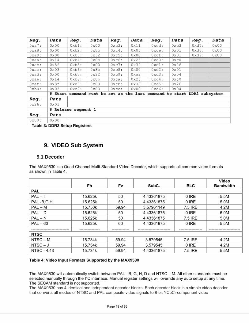
Reg. Data Reg. Data Reg. Data Reg. Data Reg. Data 0xa7: 0x00 0xb1: 0x00 0xc3: 0x11 0xcd: 0xe3 0xd7: 0x00 0xa8: 0x00 0xb2: 0x8b 0xc4: 0x0f 0xce: 0x01 0xd8: 0x00 0xa9: 0x00 0xb3: 0x32 0xc5: 0x00 0xcf: 0x01 0xd9: 0x00 0xaa: 0x14 0xb4: 0x0b 0xc6: 0x26 0xd0: 0xc0 0xab: 0x8f 0xb5: 0x00 0xc7: 0x39 0xd1: 0x26 0xac: 0x03 0xb6: 0x8b 0xc8: 0x00 0xd2: 0x01 0xad: 0x00 0xb7: 0x32 0xc9: 0xe3 0xd3: 0x04 0xae: 0x14 0xb8: 0x0b 0xca: 0x26 0xd4: 0xc0 0xaf: 0x8f 0xb9: 0x00 0xcb: 0x39 0xd5: 0x26 0xb0: 0x03 0xc2: 0x00 0xcc: 0x00 0xd6: 0x04
# Start command must be set as the last command to start DDR2 subsystem Reg. Data 0x26: 0x01 # Release segment 1 Reg. Data 0x00: 0x00 Table 3: DDR2 Setup Registers
9. VIDEO Sub System
9.1 Decoder The MAX9530 is a Quad Channel Multi-Standard Video Decoder, which supports all common video formats as shown in Table 4.
Fh Fv SubC. BLC Video
Bandwidth PAL PAL – I 15.625k 50 4.43361875 0 IRE 5.5M PAL -B,G,H 15.625k 50 4.43361875 0 IRE 5.0M PAL – M 15.750k 59.94 3.57961149 7.5 IRE 4.2M PAL – D 15.625k 50 4.43361875 0 IRE 6.0M PAL – N 15.625k 50 4.43361875 7.5 IRE 5.0M PAL – 60 15.625k 60 4.43361975 0 IRE 5.5M ---------------------------- --------------- ------------- ------------------------ ----------------- -----------------------NTSC NTSC – M 15.734k 59.94 3.579545 7.5 IRE 4.2M NTSC – J 15.734k 59.94 3.579545 0 IRE 4.2M NTSC - 4.43 15.734k 59.94 4.43361875 7.5 IRE 5.5M
Table 4: Video Input Formats Supported by the MAX9530 The MAX9530 will automatically switch between PAL - B, G, H, D and NTSC – M. All other standards must be selected manually through the I2C interface. Manual register settings will override any auto setup at any time. The SECAM standard is not supported.
Page 19 of 83
The MAX9530 has 4 identical and independent decoder blocks. Each decoder block is a simple video decoder that converts all modes of NTSC and PAL composite video signals to 8-bit YCbCr component video
compatible with the ITU-R BT.656 standard. The device powers up in a fully operational mode and automatically configures itself to standard NTSC or standard PAL. An internal 10-bit 54MHz analog-to-digital converter (ADC) samples at four times the sampling rate specified in ITU-R BT.601. The analog front-end of the MAX9530 features a DC restoration circuit, automatic gain control, and automatic offset correction. These blocks are controlled with digital processing to accurately optimize the full-scale range of the ADC. An integrated analog anti-aliasing filter eliminates the need for off-chip filtering. The system clock is generated with an external 27MHz crystal and an internal oscillator. Optionally, a 27MHz or 54MHz external clock can be connected to REF27I. An internal digital PLL is used to generate the 54MHz ADC sample clock. The MAX9530 decoder uses a 5-line adaptive comb filter to separate the luminance (Y) and chrominance (C) video components and reduce cross-chrominance and cross-luminance artifacts. The MAX9530 decoder operates with any type of standard composite video signal source including analog CCTV cameras, DVD players, navigation systems and VCRs.
9.1.1. Analog Front End (AFE) The MAX9530 AFE implements DC restoration, automatic gain control (AGC), analog anti-aliasing filter (LPF), activity detection, channel selection, and analog-to-digital conversion. The MAX9530 supports both differential and single-ended video input signals. I2C register 0x21/31/41/51 [1] is set to 1 for differential inputs and 0 for single-ended inputs. Figures 47 & 48 illustrate the schematic of analog inputs configured for differential and single-ended operation. Internally, differential signal paths are always used to process the analog video signal to minimize the effect of noise coupling. For differential inputs the common-mode input voltage is set internally. The DC restore DAC sources/sinks current into both VINP and VINN pins to set the average differential voltage so that the optimal full scale range of the ADC is used. For single ended applications an internal bias circuit sets the DC reference voltage (VREF) at the VINN pin to 850mV. This pin must be AC coupled externally to ground with a 0,1uF capacitor. The video signal must be attenuated externally with a 6dB resistive attenuator. The signals are converted to a fully differential signal by the analog AGC circuit. See Figures 47 & 48 for an external schematic that supports both differential and single-ended applications.
9.1.2. DC Restoration DAC The video inputs are AC-coupled to the MAX9530 with 0.1μF capacitors. The DC restoration circuit sets the sync level at the output of the ADC by sinking or sourcing current at the selected video input. In differential mode the DAC sources or sinks current in both AINP and AINN. In single-ended mode the DAC sources or sinks current in the AINP pin. A digital control at the ADC output is used to monitor the average sync level. An error signal is generated in the digital control block that is used by a current DAC to source or sink current to the AC-coupled input to restore the DC level. The DC restoration circuit also corrects the offset in the analog signal chain and sets the sync level at the ADC output to code 32 (decimal).
9.1.3. Analog Automatic Gain Control (Analog AGC) The MAX9530 includes an analog variable gain amplifier with a digitally controlled gain for automatic gain control (AGC). The AGC uses the sync amplitude at the output of the ADC to control the gain. For signals without copy protection, the AGC adjusts the gain until the sync amplitude is 208 (decimal) codes at the ADC output. For inputs with copy protection, the AGC automatically compensates for the reduced sync amplitude on active lines. The analog AGC loop can be disabled and the gain is set manually to 1 of 16 values using the Gain Control register 0x0A. The range of analog gain is 3.5dB to 12dB.
9.1.4. Analog Low Pass Filter (LPF) The MAX9530 includes a high-performance anti-aliasing analog low pass filter with a 3dB bandwidth of 13MHz (typ) and better than 0.25dB (typ) pass band flatness to 5MHz. This eliminates the need for external filtering on the video inputs. The filter typically provides 36dB attenuation at 53MHz (1MHz below ADC sample rate).
9.1.5. 54Msps Video ADC A 10-bit 54Msps ADC converts the filtered analog composite video signal for digital signal processing (composite video demodulation).
Page 20 of 83
9.1.6. Digital Filtering Digital filtering at the ADC output removes any out of band interference and improves the signal-to-noise ratio before decoding. The signal path includes a digital anti-aliasing low pass filter that has 1dB of pass band flatness to 5.5MHz and a minimum of 45dB of stop band attenuation for frequencies greater than 9MHz.
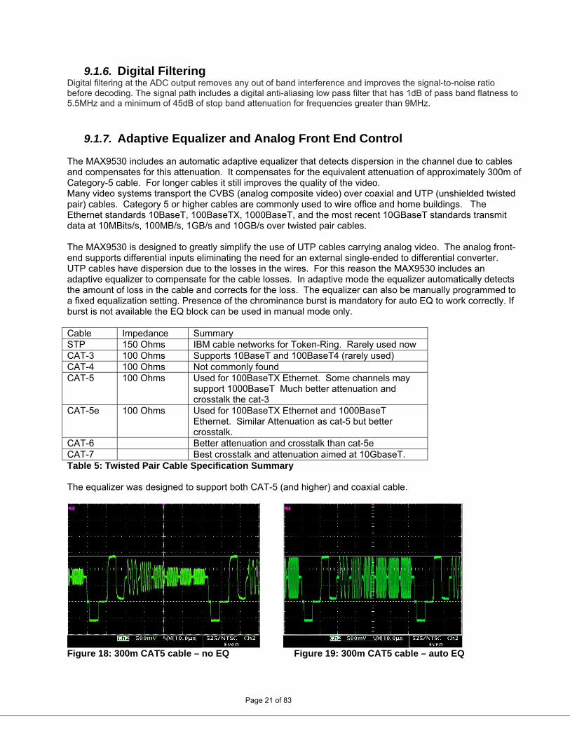
9.1.7. Adaptive Equalizer and Analog Front End Control The MAX9530 includes an automatic adaptive equalizer that detects dispersion in the channel due to cables and compensates for this attenuation. It compensates for the equivalent attenuation of approximately 300m of Category-5 cable. For longer cables it still improves the quality of the video. Many video systems transport the CVBS (analog composite video) over coaxial and UTP (unshielded twisted pair) cables. Category 5 or higher cables are commonly used to wire office and home buildings. The Ethernet standards 10BaseT, 100BaseTX, 1000BaseT, and the most recent 10GBaseT standards transmit data at 10MBits/s, 100MB/s, 1GB/s and 10GB/s over twisted pair cables. The MAX9530 is designed to greatly simplify the use of UTP cables carrying analog video. The analog front-end supports differential inputs eliminating the need for an external single-ended to differential converter. UTP cables have dispersion due to the losses in the wires. For this reason the MAX9530 includes an adaptive equalizer to compensate for the cable losses. In adaptive mode the equalizer automatically detects the amount of loss in the cable and corrects for the loss. The equalizer can also be manually programmed to a fixed equalization setting. Presence of the chrominance burst is mandatory for auto EQ to work correctly. If burst is not available the EQ block can be used in manual mode only. Cable Impedance Summary STP 150 Ohms IBM cable networks for Token-Ring. Rarely used now CAT-3 100 Ohms Supports 10BaseT and 100BaseT4 (rarely used) CAT-4 100 Ohms Not commonly found CAT-5 100 Ohms Used for 100BaseTX Ethernet. Some channels may
support 1000BaseT Much better attenuation and crosstalk the cat-3
CAT-5e 100 Ohms Used for 100BaseTX Ethernet and 1000BaseT Ethernet. Similar Attenuation as cat-5 but better crosstalk.
CAT-6 Better attenuation and crosstalk than cat-5e CAT-7 Best crosstalk and attenuation aimed at 10GbaseT. Table 5: Twisted Pair Cable Specification Summary The equalizer was designed to support both CAT-5 (and higher) and coaxial cable.
Figure 18: 300m CAT5 cable – no EQ Figure 19: 300m CAT5 cable – auto EQ
Page 21 of 83
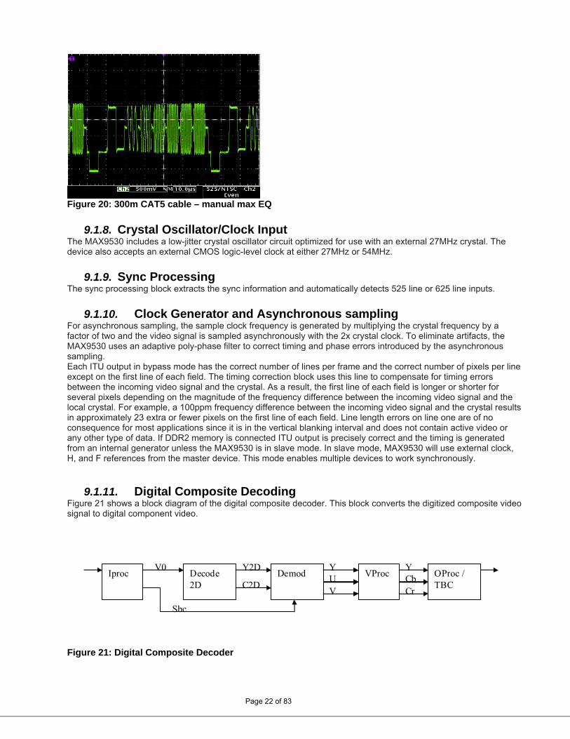
Figure 20: 300m CAT5 cable – manual max EQ
9.1.8. Crystal Oscillator/Clock Input The MAX9530 includes a low-jitter crystal oscillator circuit optimized for use with an external 27MHz crystal. The device also accepts an external CMOS logic-level clock at either 27MHz or 54MHz.
9.1.9. Sync Processing The sync processing block extracts the sync information and automatically detects 525 line or 625 line inputs.
9.1.10. Clock Generator and Asynchronous sampling For asynchronous sampling, the sample clock frequency is generated by multiplying the crystal frequency by a factor of two and the video signal is sampled asynchronously with the 2x crystal clock. To eliminate artifacts, the MAX9530 uses an adaptive poly-phase filter to correct timing and phase errors introduced by the asynchronous sampling. Each ITU output in bypass mode has the correct number of lines per frame and the correct number of pixels per line except on the first line of each field. The timing correction block uses this line to compensate for timing errors between the incoming video signal and the crystal. As a result, the first line of each field is longer or shorter for several pixels depending on the magnitude of the frequency difference between the incoming video signal and the local crystal. For example, a 100ppm frequency difference between the incoming video signal and the crystal results in approximately 23 extra or fewer pixels on the first line of each field. Line length errors on line one are of no consequence for most applications since it is in the vertical blanking interval and does not contain active video or any other type of data. If DDR2 memory is connected ITU output is precisely correct and the timing is generated from an internal generator unless the MAX9530 is in slave mode. In slave mode, MAX9530 will use external clock, H, and F references from the master device. This mode enables multiple devices to work synchronously.
9.1.11. Digital Composite Decoding Figure 21 shows a block diagram of the digital composite decoder. This block converts the digitized composite video signal to digital component video.
Iproc Decode 2D
Demod VProc OProc / TBC
V0 Y2D
C2D
Y U V
Y Cb Cr
Sbc
Figure 21: Digital Composite Decoder
Page 22 of 83
9.1.12. Sync Level Correction and Sync Extraction The sync extraction function extracts the raw sync signals from the video and the extracted sync information is sent to the sync processor. The sync level from the AFE is code 32 (decimal) on a 10-bit scale and the blanking level is approximately 208 (decimal) codes above the sync level. The sync slicer default threshold is set to approximately the middle of the sync pulse at decimal code 128. The sync slice level can optionally be manually adjusted using the slice bits in register 0x0F. The sync level correction block features an optional digital clamp that can be enabled in register 0x09. Enabling the digital clamp sets the sync level to code 0 (decimal) and gives higher frequency tracking of the input signals. When the digital clamp is enabled, the sync slice level in register 0x0F should be adjusted accordingly to provide equivalent noise rejection.
9.1.13. Sync Processor and Analog Copy Protection Detection The sync processor extracts the horizontal sync and vertical sync signals. Field pulses and burst gate pulses are generated based on VSYNC and HSYNC, respectively. The sync processing block provides sync timing to measure the sync level and amplitude for the black level control and composite AGC. The sync processor also detects incoming video signal standards (525 line NTSC and 625 line PAL). Video standard information is available in Status register 0x01. The detected video standard is used to automatically configure the decoder. The MAX9530 detects the NTSC-M (standard NTSC) and PAL B/G/H/I/D (standard PAL) standards automatically. The sync processor block also detects analog copy protection. Extracted copy protection information is available in Status register 0x01.
9.1.14. Composite Automatic Gain Control (AGC) In addition to the analog AGC that optimizes the ADC full-scale range, a digital AGC is used to more accurately set the video amplitude. The Composite AGC uses the amplitude of the sync signal to set the gain.
9.1.15. Adaptive Comb Filter The MAX9530 uses a 5-line adaptive comb filter to separate luminance and chrominance components from a single composite channel. The adaptation algorithm does not require configuration. The adaptive comb filter adjusts based on the relationship and content of video data between neighboring lines. The filter automatically adapts the comb filter structure between a 5-line filter and a notch filter.
9.1.16. Chrominance Signal Demodulator After luminance (Y) and chrominance (C) components are separated, the Y component passes through a delay line to compensate for the C component delay through the demodulator. The chrominance signal path contains an AGC before the signal demodulator. The chrominance AGC uses the color burst amplitude to set the gain. The chrominance is demodulated using a subcarrier signal locked to the burst. The demodulated chrominance signals, Cb and Cr, are low pass filtered to eliminate unwanted products of demodulation.
9.1.17. Image Enhancement and Color Correction The MAX9530 provides contrast, brightness, hue, and saturation manual control registers.
9.1.18. Time Base Correction The MAX9530 provides time base correction (TBC) to allow the decoder to properly process unstable and nonstandard video from sources such as a VCR. The time base correction minimizes the effect of sampling
Page 23 of 83
jitter to ensure that there are a correct number of pixels per active line.
9.1.19. Programmable 2D Scaler (per video input channel): The MAX9530 features a programmable scaler. The scaler can downscale a standard definition stream up to 1:1/4. Inputs and outputs to the scaler are 8-bit multiplexed UYVYUYVY video. The scaler does not de-interlace input video. The MAX9530 scaler supports CIF and QCIF video formats for PAL and NTSC. The horizontal scaling employs a dynamic 17-tap poly-phase interpolation filter for luminance and chrominance. The vertical scaling uses a simple line dropping algorithm after reducing the vertical bandwidth (3-tap FIR). Downscaling is achieved by programming the scaling ratio register. When outputting un-scaled video, the MAX9530 will output CCIR601 compatible 720 pixels per line at 13.5MHz. If the number of output pixels required is smaller than 720 in CCIR601, then compatible mode is used to reduce the output pixels to the desired number.
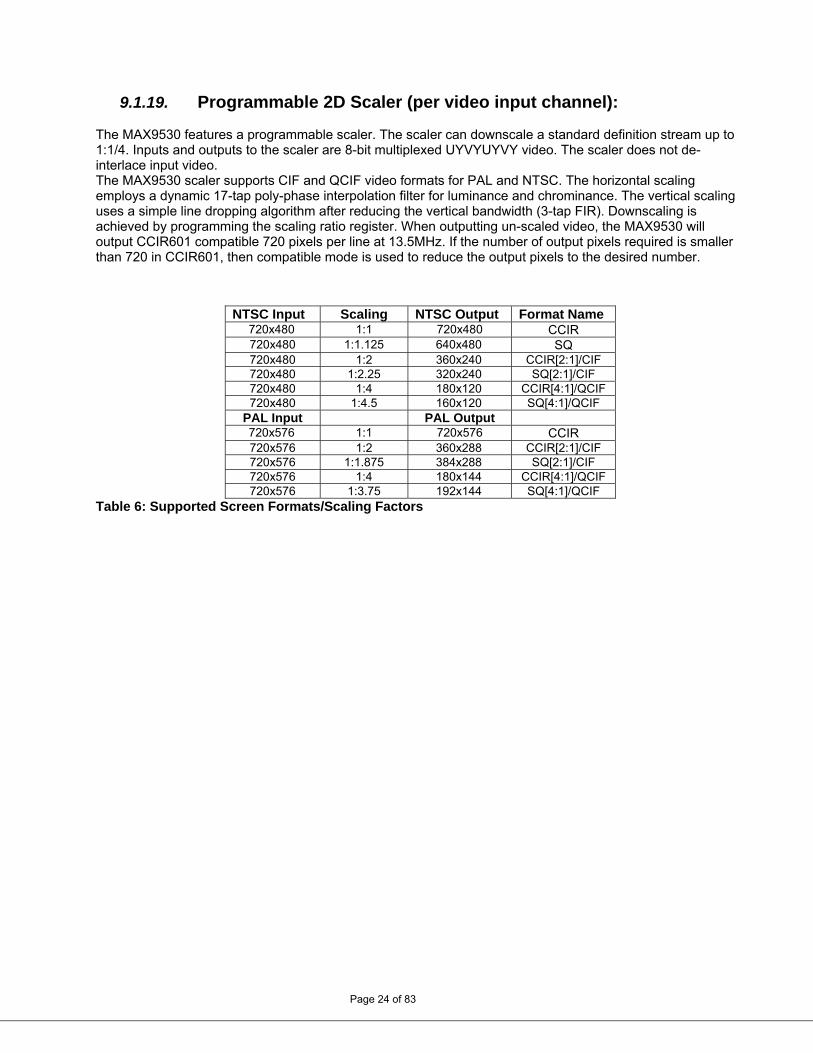
NTSC Input Scaling NTSC Output Format Name 720x480 1:1 720x480 CCIR 720x480 1:1.125 640x480 SQ 720x480 1:2 360x240 CCIR[2:1]/CIF 720x480 1:2.25 320x240 SQ[2:1]/CIF 720x480 1:4 180x120 CCIR[4:1]/QCIF 720x480 1:4.5 160x120 SQ[4:1]/QCIF
PAL Input PAL Output 720x576 1:1 720x576 CCIR 720x576 1:2 360x288 CCIR[2:1]/CIF 720x576 1:1.875 384x288 SQ[2:1]/CIF 720x576 1:4 180x144 CCIR[4:1]/QCIF 720x576 1:3.75 192x144 SQ[4:1]/QCIF
Table 6: Supported Screen Formats/Scaling Factors
Page 24 of 83
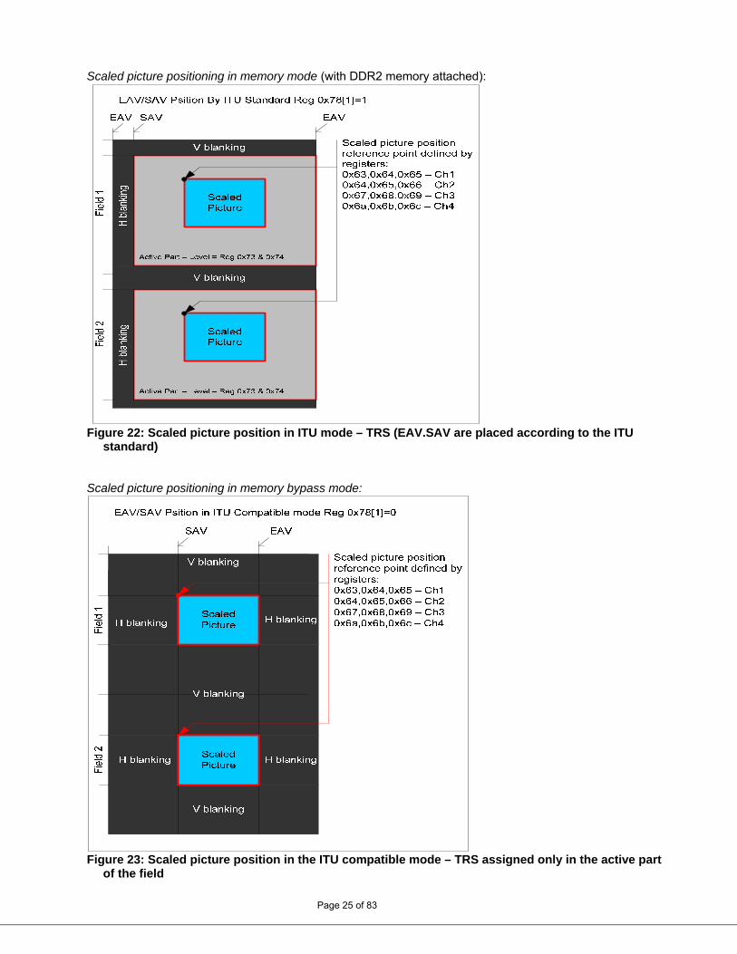
Scaled picture positioning in memory mode (with DDR2 memory attached):
Figure 22: Scaled picture position in ITU mode – TRS (EAV.SAV are placed according to the ITU
standard) Scaled picture positioning in memory bypass mode:
Page 25 of 83
Figure 23: Scaled picture position in the ITU compatible mode – TRS assigned only in the active part of the field
Video data for the scaled picture will contain SAV and EAV codes for each line with active video data for the scaled picture. All other lines will be assigned as H or V blanking. To acquire data for the scaled picture the user can program Tpp 1, 2, 3 or 4 to be a data valid signal or use EAV/SAV detection.
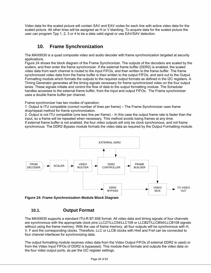
10. Frame Synchronization The MAX9530 is a quad composite video and audio decoder with frame synchronization targeted at security applications. Figure 24 shows the block diagram of the Frame Synchronizer. The outputs of the decoders are scaled by the scalers, and then enter the frame synchronizer. If the external frame buffer (DDR2) is enabled, the scaled video data from each channel is routed to the input FIFOs, and then written to the frame buffer. The frame synchronized video data from the frame buffer is then written to the output FIFOs, and sent out to the Output Formatting module which formats the outputs to the required output formats as defined in the I2C registers. A Timing Generator generates all the timing signals necessary for frame synchronized video on the four output lanes. These signals initiate and control the flow of data to the output formatting module. The Scheduler handles accesses to the external frame buffer, from the input and output FIFOs. The Frame synchronizer uses a double frame buffer per channel. Frame synchronizer has two modes of operation: 1. Output is ITU compatible (correct number of lines per frame) – The Frame Synchronizer uses frame drop/repeat method for frame synchronization. 2. Output is not ITU compatible (one less line per frame) – In this case the output frame rate is faster than the input, so a frame will be repeated when necessary. This method avoids losing frames at any time. If external frame buffer is not enabled. the four video outputs will only be clock synchronous, and not frame synchronous. The DDR2 Bypass module formats the video data as required by the Output Formatting module.
FROMDECODER
SCALERVIDEO
ROUTERDDR2
CONTROLLER
EXTERNAL DDR2
FRAMEBUILDER
VIDEOMUX
DDR2BYPASS
TO VIDEOOUT
Figure 24: Frame Synchronization Module Block Diagram
10.1. Output Format The MAX9530 supports a standard ITU-R BT.656 format. All video data and timing signals of four channels are synchronous with the appropriate clock pins LLC27/LLC54/LLC108 or LLCB27/LLCB54/LLCB108 signals without using the frame memory. With the use of frame memory, all four outputs will be synchronous with H, V, F and the corresponding clocks. Therefore, LLC or LLCB clocks with Href and Fref can be connected to four channel interfaces for synchronizing data.
Page 26 of 83
The output formatting module receives video data from the Video Output FIFOs (if external DDR2 is used) or from the Video Input FIFOs (if DDR2 is bypassed). This module then formats and outputs the video data on the four video output ports, as per the I2C register settings.
The video output formats supported are described in the following sections.
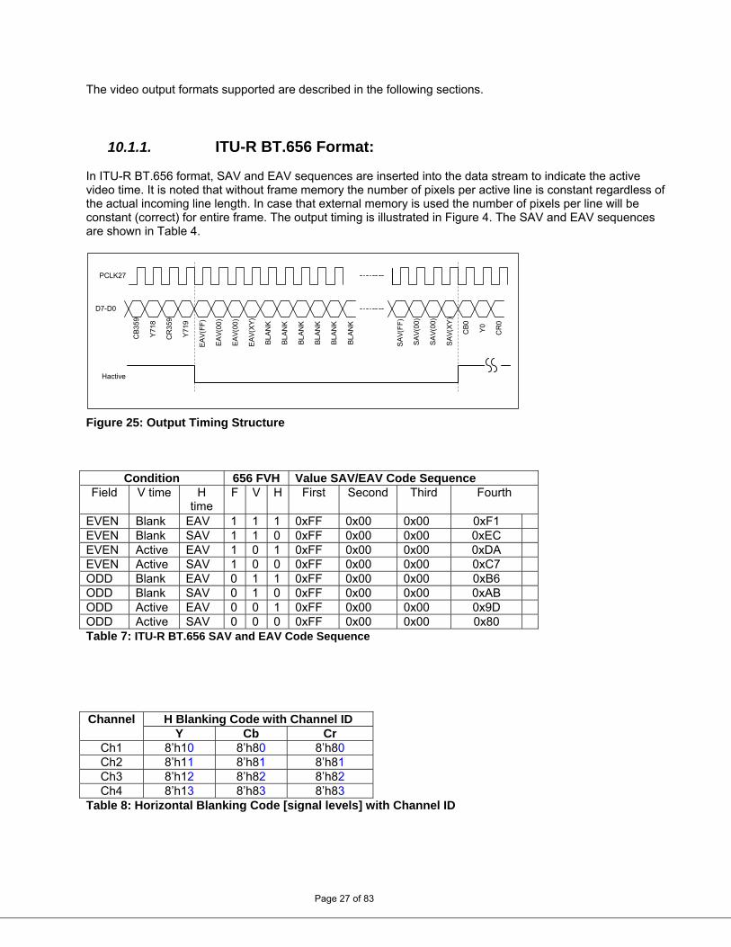
10.1.1. ITU-R BT.656 Format: In ITU-R BT.656 format, SAV and EAV sequences are inserted into the data stream to indicate the active video time. It is noted that without frame memory the number of pixels per active line is constant regardless of the actual incoming line length. In case that external memory is used the number of pixels per line will be constant (correct) for entire frame. The output timing is illustrated in Figure 4. The SAV and EAV sequences are shown in Table 4.
CB
359
Y71
8
CR
359
Y71
9
EA
V(F
F)
BL
AN
K
CB
0
Y0
CR
0
EA
V(0
0)
EA
V(0
0)
EA
V(X
Y)
BL
AN
K
BL
AN
K
BL
AN
K
BL
AN
K
BL
AN
K
SA
V(F
F)
SA
V(0
0)
SA
V(0
0)
SA
V(X
Y)
PCLK27
D7-D0
Hactive
Figure 25: Output Timing Structure
Condition 656 FVH Value SAV/EAV Code Sequence Field V time H
time F V H First Second Third Fourth
EVEN Blank EAV 1 1 1 0xFF 0x00 0x00 0xF1 EVEN Blank SAV 1 1 0 0xFF 0x00 0x00 0xEC EVEN Active EAV 1 0 1 0xFF 0x00 0x00 0xDA EVEN Active SAV 1 0 0 0xFF 0x00 0x00 0xC7 ODD Blank EAV 0 1 1 0xFF 0x00 0x00 0xB6 ODD Blank SAV 0 1 0 0xFF 0x00 0x00 0xAB ODD Active EAV 0 0 1 0xFF 0x00 0x00 0x9D ODD Active SAV 0 0 0 0xFF 0x00 0x00 0x80 Table 7: ITU-R BT.656 SAV and EAV Code Sequence
H Blanking Code with Channel ID Channel Y Cb Cr
Ch1 8’h10 8’h80 8’h80 Ch2 8’h11 8’h81 8’h81 Ch3 8’h12 8’h82 8’h82 Ch4 8’h13 8’h83 8’h83
Table 8: Horizontal Blanking Code [signal levels] with Channel ID
Page 27 of 83
Condition 656 FVH Value SAV/EAV Code Sequence
Fourth – TW Ch ID Field V time
H time
F V H First Second
Third Ch1 Ch2 Ch3 Ch4
EVEN Blank EAV 1 1 1 0xFF 0x00 0x00 0xF0 0xF1 0xF2 0xF3 EVEN Blank SAV 1 1 0 0xFF 0x00 0x00 0xE0 0xE1 0xE2 0xE3 EVEN Active EAV 1 0 1 0xFF 0x00 0x00 0xD0 0xD1 0xD2 0xD3 EVEN Active SAV 1 0 0 0xFF 0x00 0x00 0xC0 0xC1 0xC2 0xC3 ODD Blank EAV 0 1 1 0xFF 0x00 0x00 0xB0 0xB1 0xB2 0xB3 ODD Blank SAV 0 1 0 0xFF 0x00 0x00 0xA0 0xA1 0xA2 0xA3 ODD Active EAV 0 0 1 0xFF 0x00 0x00 0x90 0x91 0x92 0x93 ODD Active SAV 0 0 0 0xFF 0x00 0x00 0x80 0x81 0x82 0x83
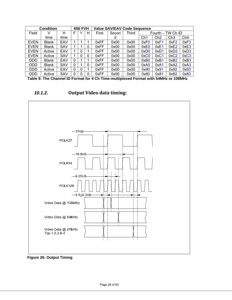
Table 9: The Channel ID Format for 4 Ch Time-multiplexed Format with 54MHz or 108MHz
10.1.2. Output Video data timing:
Figure 26: Output Timing
Page 28 of 83
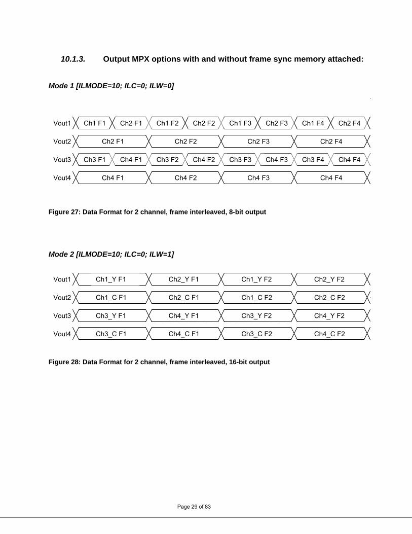
10.1.3. Output MPX options with and without frame sync memory attached: Mode 1 [ILMODE=10; ILC=0; ILW=0]
Figure 27: Data Format for 2 channel, frame interleaved, 8-bit output Mode 2 [ILMODE=10; ILC=0; ILW=1]
Figure 28: Data Format for 2 channel, frame interleaved, 16-bit output
Page 29 of 83
Vout1
Vout2 Ch1_C F1 Ch2_C F1 Ch1_C F2
Vout3
Vout4
Ch1_Y F1 Ch2_Y F1 Ch1_Y F2
Ch3_Y F1 Ch4_Y F1 Ch3_Y F2
Ch2_C F2
Ch2_Y F2
Ch4_Y F2
Ch3_C F1 Ch4_C F1 Ch3_C F2 Ch4_C F2
Vout1
Vout2 Ch2 F1 Ch2 F2 Ch2 F3
Vout3
Vout4
Ch1 F1 Ch1 F2 Ch1 F3
Ch2 F4
Ch1 F4 Ch2 F3
Ch4 F1 Ch4 F2 Ch4 F3 Ch4 F4
Ch4 F4Ch4 F3Ch4 F2Ch4 F1 Ch3 F1 Ch3 F2 Ch3 F3 Ch3 F4
Ch2 F4Ch2 F2Ch2 F1

Mode 3 [ILMODE=10; ILC=1; ILW=0]
Figure 29: Data Format for 4 channel, frame interleaved, 8-bit output Mode 4 [ILMODE=10; ILC=1; ILW=1]
Figure 30: Data Format for 4 channel, frame interleaved, 16-bit output
Page 30 of 83
Vout1
Vout2
Vout3
Vout4 Ch4_C F2 Ch2_C F2 Ch4_C F1 Ch2_C F1 Ch1_C F1 Ch3_C F1 Ch1_C F2 Ch3_C F2
Ch1 F1 Ch1 F2
Ch2 F1 Ch2 F2
Ch4_Y F2 Ch2_Y F2 Ch4_Y F1 Ch2_Y F1 Ch1_Y F1 Ch3_Y F1 Ch1_Y F2 Ch3_Y F2
Vout1
Vout2
Vout3
Vout4 Ch4 F2Ch2 F2Ch4 F1Ch2 F1 Ch1 F1 Ch3 F1 Ch1 F2 Ch3 F2
Ch1 F1 Ch1 F2
Ch2 F1 Ch2 F2
Ch3 F1 Ch3 F2
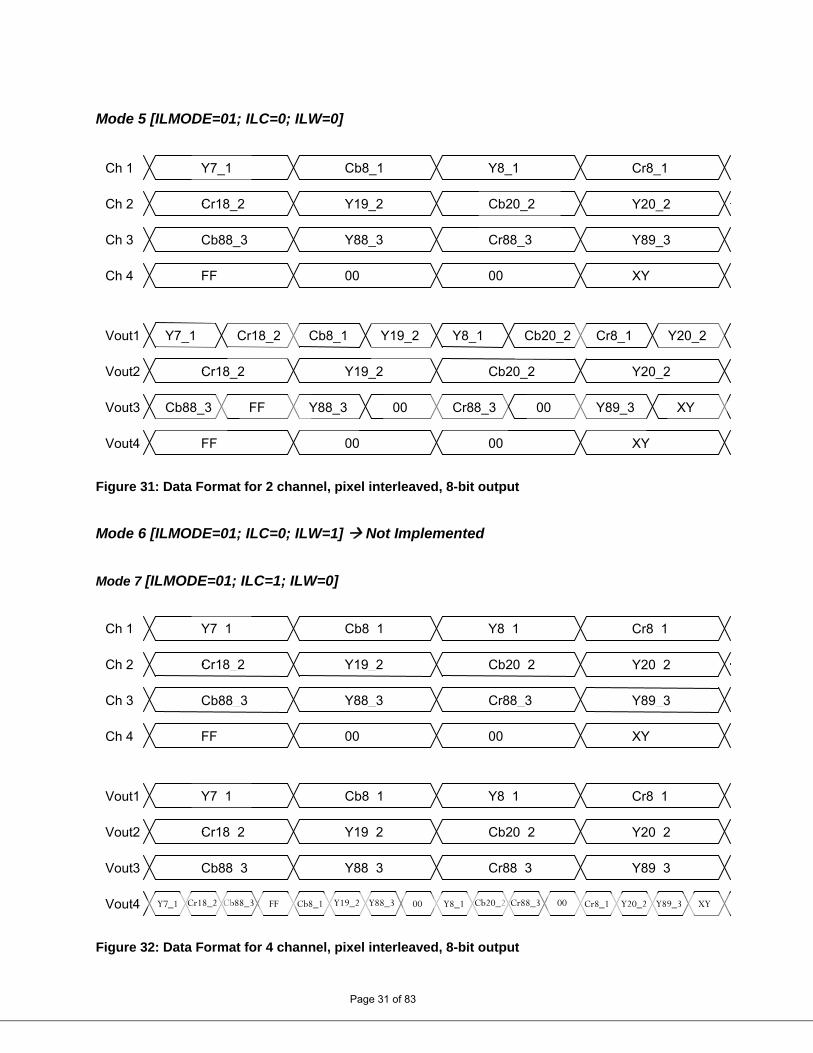
Mode 5 [ILMODE=01; ILC=0; ILW=0]
Figure 31: Data Format for 2 channel, pixel interleaved, 8-bit output Mode 6 [ILMODE=01; ILC=0; ILW=1] Not Implemented Mode 7 [ILMODE=01; ILC=1; ILW=0]
Figure 32: Data Format for 4 channel, pixel interleaved, 8-bit output
Page 31 of 83
Ch 1
Ch 2
Ch 3
Ch 4
Vout1
Vout2 Cr18_2 Y19_2 Cb20_2
Vout3
Vout4
Y7_1 Cb8_1 Y8_1
Cb88_3 Y88_3 Cr88_3
Y7_1 Cb88_3 Cr18_2 FF
Y20_2
Cr8_1
Y89_3
Cr18_2 Y19_2 Cb20_2
Y7_1 Cb8_1 Y8_1
Cb88_3 Y88_3 Cr88_3
Y20_2
Cr8_1
Y89_3
FF 00 00 XY
Cb8_1 Y19_2 Y88_3 00 Y8_1 Cb20_2 Cr88_3 00 Cr8_1 Y20_2 Y89_3 XY
Ch 1
Ch 2
Ch 3
Ch 4
Vout1
Vout2 Cr18_2 Y19_2 Cb20_2
Vout3
Vout4
Y7_1 Cb8_1 Y8_1
Y20_2
Cr8_1
Cr18_2 Y19_2
Cb20_2
Y7_1 Cb8_1 Y8_1
Cb88_3 Y88_3 Cr88_3
Y20_2
Cr8_1
Y89_3
FF 00 00 XY
FF 00 00 XY
Cr18_2 Y19_2 Y20_2
XY0000FF Cb88_3 Y88_3 Cr88_3 Y89_3
Cb20_2
Mode 8 [ILMODE=01; ILC=1; ILW=1] Not Implemented
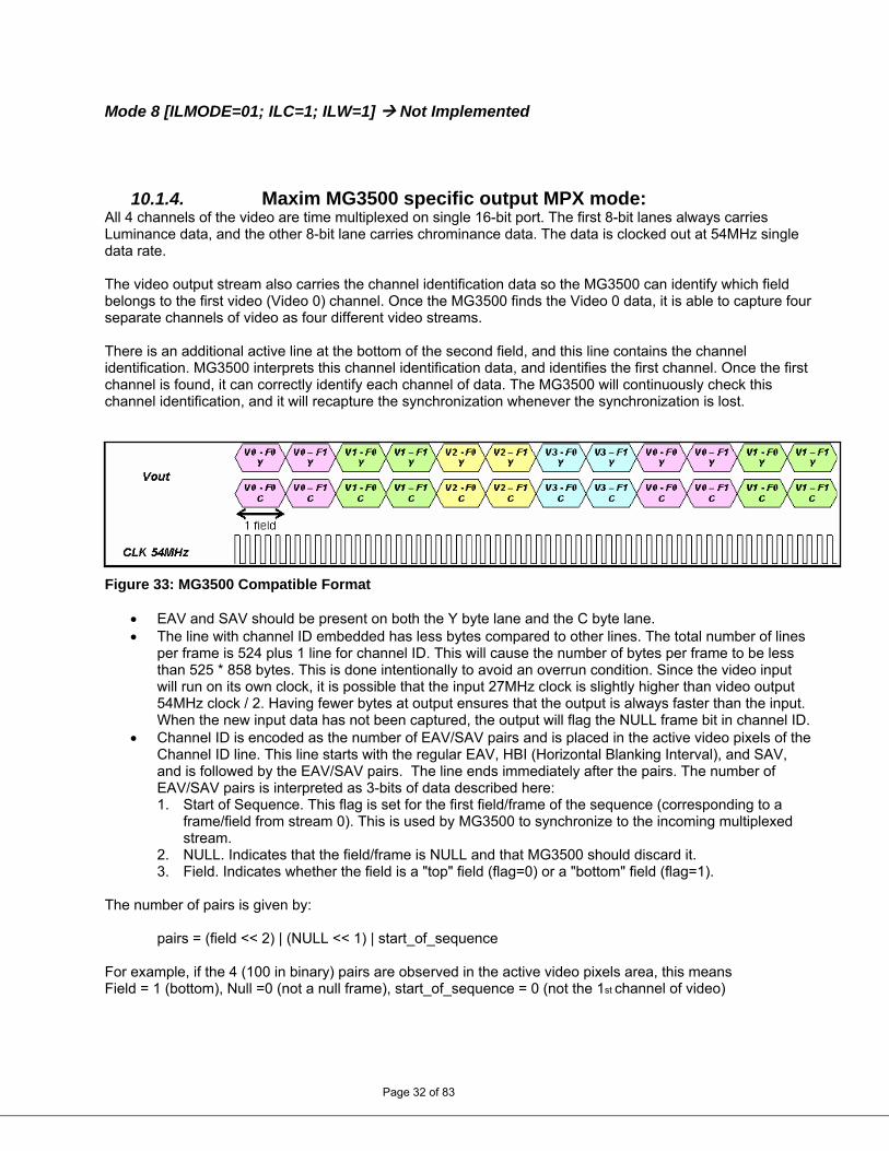
10.1.4. Maxim MG3500 specific output MPX mode: All 4 channels of the video are time multiplexed on single 16-bit port. The first 8-bit lanes always carries Luminance data, and the other 8-bit lane carries chrominance data. The data is clocked out at 54MHz single data rate. The video output stream also carries the channel identification data so the MG3500 can identify which field belongs to the first video (Video 0) channel. Once the MG3500 finds the Video 0 data, it is able to capture four separate channels of video as four different video streams. There is an additional active line at the bottom of the second field, and this line contains the channel identification. MG3500 interprets this channel identification data, and identifies the first channel. Once the first channel is found, it can correctly identify each channel of data. The MG3500 will continuously check this channel identification, and it will recapture the synchronization whenever the synchronization is lost.
Figure 33: MG3500 Compatible Format
EAV and SAV should be present on both the Y byte lane and the C byte lane. The line with channel ID embedded has less bytes compared to other lines. The total number of lines
per frame is 524 plus 1 line for channel ID. This will cause the number of bytes per frame to be less than 525 * 858 bytes. This is done intentionally to avoid an overrun condition. Since the video input will run on its own clock, it is possible that the input 27MHz clock is slightly higher than video output 54MHz clock / 2. Having fewer bytes at output ensures that the output is always faster than the input. When the new input data has not been captured, the output will flag the NULL frame bit in channel ID.
Channel ID is encoded as the number of EAV/SAV pairs and is placed in the active video pixels of the Channel ID line. This line starts with the regular EAV, HBI (Horizontal Blanking Interval), and SAV, and is followed by the EAV/SAV pairs. The line ends immediately after the pairs. The number of EAV/SAV pairs is interpreted as 3-bits of data described here: 1. Start of Sequence. This flag is set for the first field/frame of the sequence (corresponding to a
frame/field from stream 0). This is used by MG3500 to synchronize to the incoming multiplexed stream.
2. NULL. Indicates that the field/frame is NULL and that MG3500 should discard it. 3. Field. Indicates whether the field is a "top" field (flag=0) or a "bottom" field (flag=1).
The number of pairs is given by:
pairs = (field << 2) | (NULL << 1) | start_of_sequence
For example, if the 4 (100 in binary) pairs are observed in the active video pixels area, this means Field = 1 (bottom), Null =0 (not a null frame), start_of_sequence = 0 (not the 1st channel of video)
Page 32 of 83
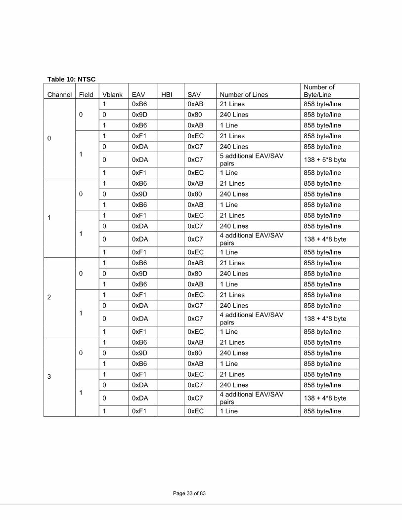
Table 10: NTSC
Channel Field Vblank EAV HBI SAV Number of Lines Number of Byte/Line
1 0xB6 0xAB 21 Lines 858 byte/line
0 0x9D 0x80 240 Lines 858 byte/line 0
1 0xB6 0xAB 1 Line 858 byte/line
1 0xF1 0xEC 21 Lines 858 byte/line
0 0xDA 0xC7 240 Lines 858 byte/line
0 0xDA 5 additional EAV/SAV
pairs 0xC7 138 + 5*8 byte
0
1
1 0xF1 0xEC 1 Line 858 byte/line
1 0xB6 0xAB 21 Lines 858 byte/line
0 0x9D 0x80 240 Lines 858 byte/line 0
1 0xB6 0xAB 1 Line 858 byte/line
1 0xF1 0xEC 21 Lines 858 byte/line
0 0xDA 0xC7 240 Lines 858 byte/line
0 0xDA 4 additional EAV/SAV
pairs 0xC7 138 + 4*8 byte
1
1
1 0xF1 0xEC 1 Line 858 byte/line
1 0xB6 0xAB 21 Lines 858 byte/line
0 0x9D 0x80 240 Lines 858 byte/line 0
1 0xB6 0xAB 1 Line 858 byte/line
1 0xF1 0xEC 21 Lines 858 byte/line
0 0xDA 0xC7 240 Lines 858 byte/line
0 0xDA 4 additional EAV/SAV
pairs 0xC7 138 + 4*8 byte
2
1
1 0xF1 0xEC 1 Line 858 byte/line
1 0xB6 0xAB 21 Lines 858 byte/line
0 0x9D 0x80 240 Lines 858 byte/line 0
1 0xB6 0xAB 1 Line 858 byte/line
1 0xF1 0xEC 21 Lines 858 byte/line
0 0xDA 0xC7 240 Lines 858 byte/line
0 0xDA 4 additional EAV/SAV
pairs 0xC7 138 + 4*8 byte
3
1
1 0xF1 0xEC 1 Line 858 byte/line
Page 33 of 83
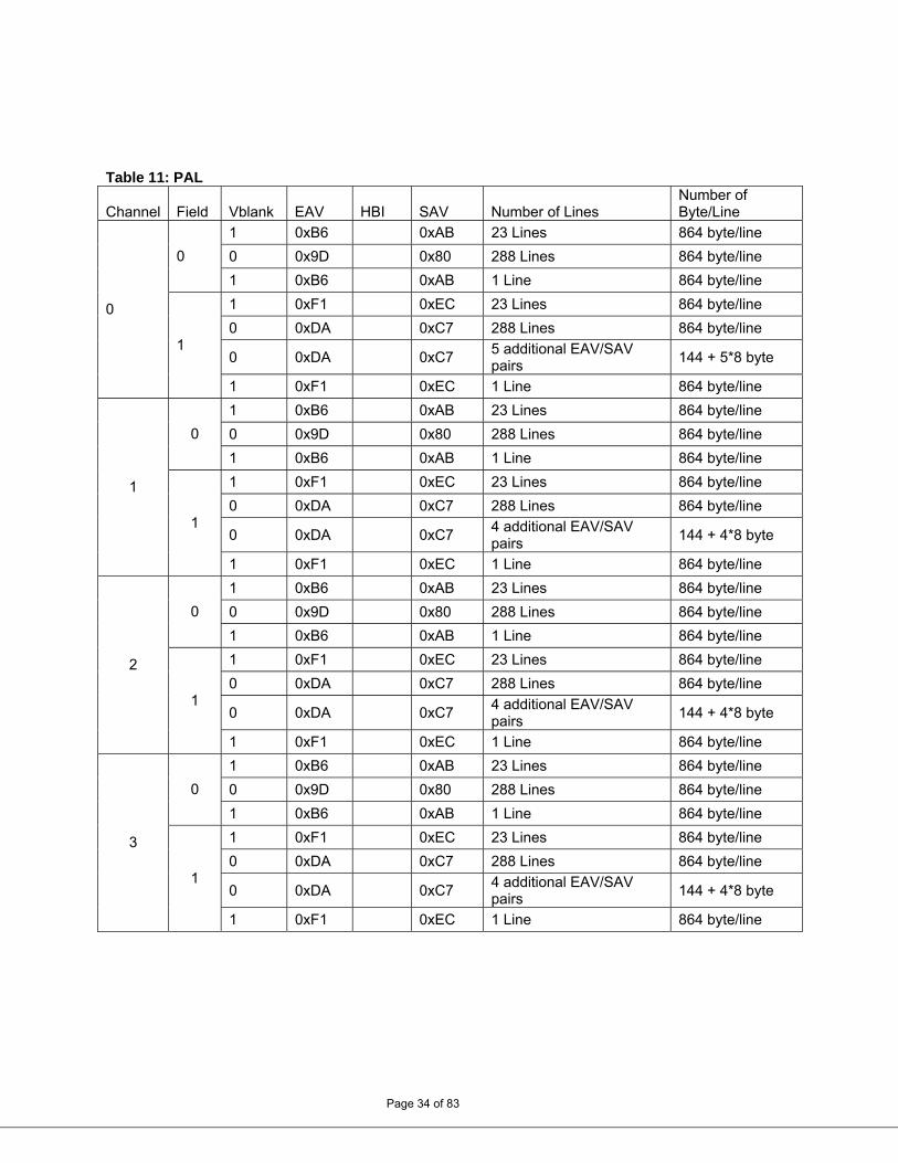
Table 11: PAL
Channel Field Vblank EAV HBI SAV Number of Lines Number of Byte/Line
1 0xB6 0xAB 23 Lines 864 byte/line
0 0x9D 0x80 288 Lines 864 byte/line 0
1 0xB6 0xAB 1 Line 864 byte/line
1 0xF1 0xEC 23 Lines 864 byte/line
0 0xDA 0xC7 288 Lines 864 byte/line
0 0xDA 5 additional EAV/SAV
pairs 0xC7 144 + 5*8 byte
0
1
1 0xF1 0xEC 1 Line 864 byte/line
1 0xB6 0xAB 23 Lines 864 byte/line
0 0x9D 0x80 288 Lines 864 byte/line 0
1 0xB6 0xAB 1 Line 864 byte/line
1 0xF1 0xEC 23 Lines 864 byte/line
0 0xDA 0xC7 288 Lines 864 byte/line
0 0xDA 4 additional EAV/SAV
pairs 0xC7 144 + 4*8 byte
1
1
1 0xF1 0xEC 1 Line 864 byte/line
1 0xB6 0xAB 23 Lines 864 byte/line
0 0x9D 0x80 288 Lines 864 byte/line 0
1 0xB6 0xAB 1 Line 864 byte/line
1 0xF1 0xEC 23 Lines 864 byte/line
0 0xDA 0xC7 288 Lines 864 byte/line
0 0xDA 4 additional EAV/SAV
pairs 0xC7 144 + 4*8 byte
2
1
1 0xF1 0xEC 1 Line 864 byte/line
1 0xB6 0xAB 23 Lines 864 byte/line
0 0x9D 0x80 288 Lines 864 byte/line 0
1 0xB6 0xAB 1 Line 864 byte/line
1 0xF1 0xEC 23 Lines 864 byte/line
0 0xDA 0xC7 288 Lines 864 byte/line
0 0xDA 4 additional EAV/SAV
pairs 0xC7 144 + 4*8 byte
3
1
1 0xF1 0xEC 1 Line 864 byte/line
Page 34 of 83
10.2. Extra Sync Output: The additional timing information such as syncs and field flag are also supported through the TPPx pins. The Hsync, Vsync and field flag timings are controlled by I2C registers and can be set to follow EAV/SAV information or to be “H_Valid or V_Valid”. If the scaler is not active the two modes are identical. If the scaler is active “H_Valid and V_Valid” will point to the active part of the scaled picture. This is especially important if the MAX9530 is used in memory bypass mode because in bypass mode the scaled frame data are output in bursts (data output is not continuous).
11. Audio Subsystem
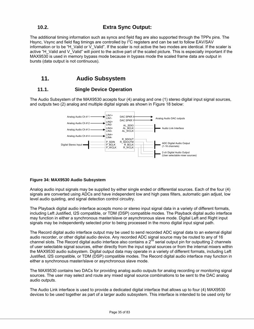
11.1. Single Device Operation
The Audio Subsystem of the MAX9530 accepts four (4) analog and one (1) stereo digital input signal sources, and outputs two (2) analog and multiple digital signals as shown in Figure 18 below:
AL_BCLKAL_WCLK
AL_SDIO
R_BCLKR_WCLK
R_SDOUTR_SDOUTM
P_BCLKP_WCLK
P_SDIN
DAC SPKR XLIN1-LIN1+
LIN2-LIN2+
LIN3-LIN3+
LIN4-LIN4+
Audio Link Interface
Analog Audio DAC outputs
Digital Stereo Input
Analog Audio Ch # 1
Analog Audio Ch # 2
Analog Audio Ch # 3
Analog Audio Ch # 4
ADC Digital Audio Output(1-16 channels)
DAC SPKR Y
2-ch Digital Audio Output(User selectable mixer sources)
Figure 34: MAX9530 Audio Subsystem Analog audio input signals may be supplied by either single ended or differential sources. Each of the four (4) signals are converted using ADCs and have independent low and high pass filters, automatic gain adjust, low level audio quieting, and signal detection control circuitry. The Playback digital audio interface accepts mono or stereo input signal data in a variety of different formats, including Left Justified, I2S compatible, or TDM (DSP) compatible modes. The Playback digital audio interface may function in either a synchronous master/slave or asynchronous slave mode. Digital Left and Right input signals may be independently selected prior to being processed in the mono digital input signal path. The Record digital audio interface output may be used to send recorded ADC signal data to an external digital audio recorder, or other digital audio device. Any recorded ADC signal source may be routed to any of 16 channel slots. The Record digital audio interface also contains a 2nd serial output pin for outputting 2 channels of user selectable signal sources, either directly from the input signal sources or from the internal mixers within the MAX9530 audio subsystem. Digital output data may operate in a variety of different formats, including Left Justified, I2S compatible, or TDM (DSP) compatible modes. The Record digital audio interface may function in either a synchronous master/slave or asynchronous slave mode. The MAX9530 contains two DACs for providing analog audio outputs for analog recording or monitoring signal sources. The user may select and route any mixed signal source combinations to be sent to the DAC analog audio outputs.
Page 35 of 83
The Audio Link interface is used to provide a dedicated digital interface that allows up to four (4) MAX9530 devices to be used together as part of a larger audio subsystem. This interface is intended to be used only for
MAX9530 link operation, but could be utilized as an additional 16 channel TDM (DSP) interface if required in special instances.
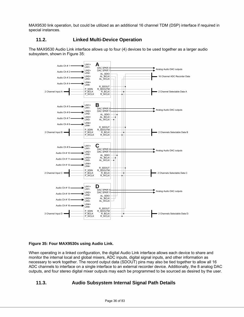
11.2. Linked Multi-Device Operation The MAX9530 Audio Link interface allows up to four (4) devices to be used together as a larger audio subsystem, shown in Figure 35:
AL_BCLKAL_WCLK
AL_SDIO
R_BCLKR_WCLK
R_SDOUTR_SDOUTM
P_BCLKP_WCLK
P_SDIN
LIN1-LIN1+
LIN2-LIN2+
LIN3-LIN3+
LIN4-LIN4+
AL_BCLKAL_WCLK
AL_SDIO
R_BCLKR_WCLK
R_SDOUTR_SDOUTM
P_BCLKP_WCLK
P_SDIN
LIN1-LIN1+
LIN2-LIN2+
LIN3-LIN3+
LIN4-LIN4+
AL_BCLKAL_WCLK
AL_SDIO
R_BCLKR_WCLK
R_SDOUTR_SDOUTM
P_BCLKP_WCLK
P_SDIN
LIN1-LIN1+
LIN2-LIN2+
LIN3-LIN3+
LIN4-LIN4+
AL_BCLKAL_WCLK
AL_SDIO
R_BCLKR_WCLK
R_SDOUTR_SDOUTM
P_BCLKP_WCLK
P_SDIN
LIN1-LIN1+
LIN2-LIN2+
LIN3-LIN3+
LIN4-LIN4+
16 Channel ADC Recorder Data
2 Channel Selectable Data A
2 Channels Selectable Data B
2 Channel Input D 2 Channels Selectable Data D:
2 Channel Input C
2 Channel Input A
2 Channel Input B
Audio Ch # 1
Audio Ch # 2
Audio Ch # 3
Audio Ch # 4
Audio Ch # 5
Audio Ch # 6
Audio Ch # 7
Audio Ch # 8
Audio Ch # 9
Audio Ch # 10
Audio Ch # 11
Audio Ch # 12
Audio Ch # 13
Audio Ch # 14
Audio Ch # 15
Audio Ch # 16
2 Channels Selectable Data C
A
B
C
D
DAC SPKR XAnalog Audio DAC outputsDAC SPKR Y
DAC SPKR XAnalog Audio DAC outputsDAC SPKR Y
DAC SPKR XAnalog Audio DAC outputs
DAC SPKR Y
DAC SPKR X Analog Audio DAC outputsDAC SPKR Y
Figure 35: Four MAX9530s using Audio Link. When operating in a linked configuration, the digital Audio Link interface allows each device to share and monitor the internal local and global mixers, ADC inputs, digital signal inputs, and other information as necessary to work together. The record output data (SDOUT) pins may also be tied together to allow all 16 ADC channels to interface on a single interface to an external recorder device. Additionally, the 8 analog DAC outputs, and four stereo digital mixer outputs may each be programmed to be sourced as desired by the user.
11.3. Audio Subsystem Internal Signal Path Details
Page 36 of 83
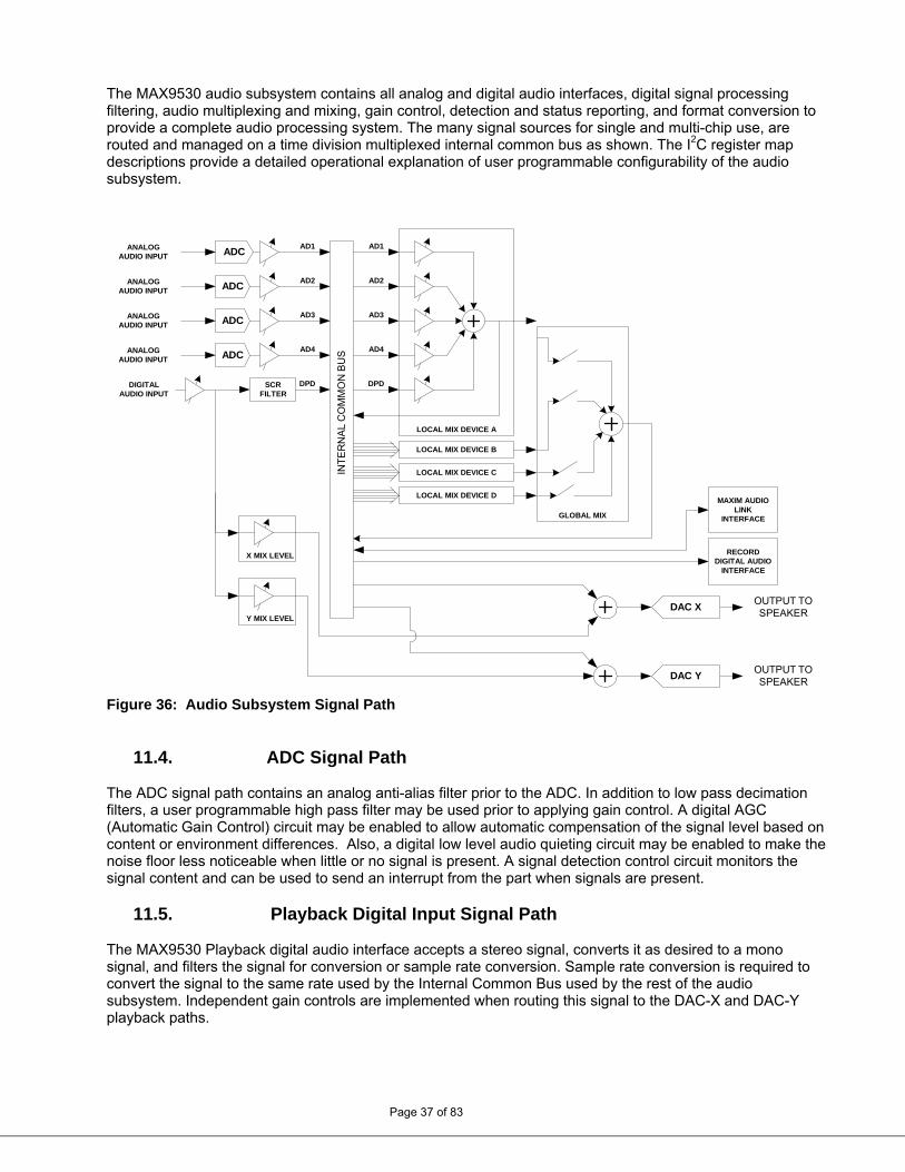
The MAX9530 audio subsystem contains all analog and digital audio interfaces, digital signal processing filtering, audio multiplexing and mixing, gain control, detection and status reporting, and format conversion to provide a complete audio processing system. The many signal sources for single and multi-chip use, are routed and managed on a time division multiplexed internal common bus as shown. The I2C register map descriptions provide a detailed operational explanation of user programmable configurability of the audio subsystem.
DIGITALAUDIO INPUT
SCRFILTER
INT
ER
NA
L C
OM
MO
N B
US
MAXIM AUDIOLINK
INTERFACE
OUTPUT TOSPEAKER
RECORDDIGITAL AUDIO
INTERFACE
ANALOGAUDIO INPUT
ADCANALOGAUDIO INPUT
ANALOGAUDIO INPUT
ANALOGAUDIO INPUT
DAC X
OUTPUT TOSPEAKER
DAC Y
AD1
AD2
AD3
AD4
DPD
ADC
ADC
ADC
AD1
AD2
AD3
AD4
DPD
LOCAL MIX DEVICE A
LOCAL MIX DEVICE B
LOCAL MIX DEVICE C
LOCAL MIX DEVICE D
GLOBAL MIX
X MIX LEVEL
Y MIX LEVEL
Figure 36: Audio Subsystem Signal Path
11.4. ADC Signal Path The ADC signal path contains an analog anti-alias filter prior to the ADC. In addition to low pass decimation filters, a user programmable high pass filter may be used prior to applying gain control. A digital AGC (Automatic Gain Control) circuit may be enabled to allow automatic compensation of the signal level based on content or environment differences. Also, a digital low level audio quieting circuit may be enabled to make the noise floor less noticeable when little or no signal is present. A signal detection control circuit monitors the signal content and can be used to send an interrupt from the part when signals are present.
11.5. Playback Digital Input Signal Path The MAX9530 Playback digital audio interface accepts a stereo signal, converts it as desired to a mono signal, and filters the signal for conversion or sample rate conversion. Sample rate conversion is required to convert the signal to the same rate used by the Internal Common Bus used by the rest of the audio subsystem. Independent gain controls are implemented when routing this signal to the DAC-X and DAC-Y playback paths.
Page 37 of 83
11.6. Internal Mixers There are two digital mixers connected to the Internal Common Bus. The first, Local Mixer, is dedicated to mixing the 5 local input signal sources using the I2C programmable level controls, and outputs the result back to the ICB so that it may be routed as desired by the user to the SDOUTM, or DAC X/Y outputs. The result is also sent to the Audio Link so it can be used by the other linked MAX9530 devices if required. The second, Global Mixer, is only useful when using the Audio Link. It allows each linked device’s Local Mixer output to be combined together. Although the user may control which local mixer signals are enabled to the global mixer, no additional level control is available. The Global Mixer may be routed as desired by the user to the SDOUTM, or DAC X/Y outputs. The result is also sent to the Audio Link so it can be routed to other devices outputs if required.
11.7. DAC-X and DAC-Y Signal Path Any signal present on the Internal Common Bus may be independently selected for conversion in the DAC-X and DAC-Y outputs. The digital audio input from the Playback interface may be mixed with the selected signals.
11.8. Record and Mixer Digital Output The Record digital audio interface contains two (2) serial output pins. The SDOUT is used to output up to 16 channels of recorded ADC signal data. The SDOUT is used to output 2 channels of selected signal sources from the Internal Common Bus, which includes the ADCs, Local and Global Mixers, and digital input signal source.
Page 38 of 83
Signal data may be output in either an 8 or 16 bit format, and with or without A-law or u-Law companding.
Page 39 of 83
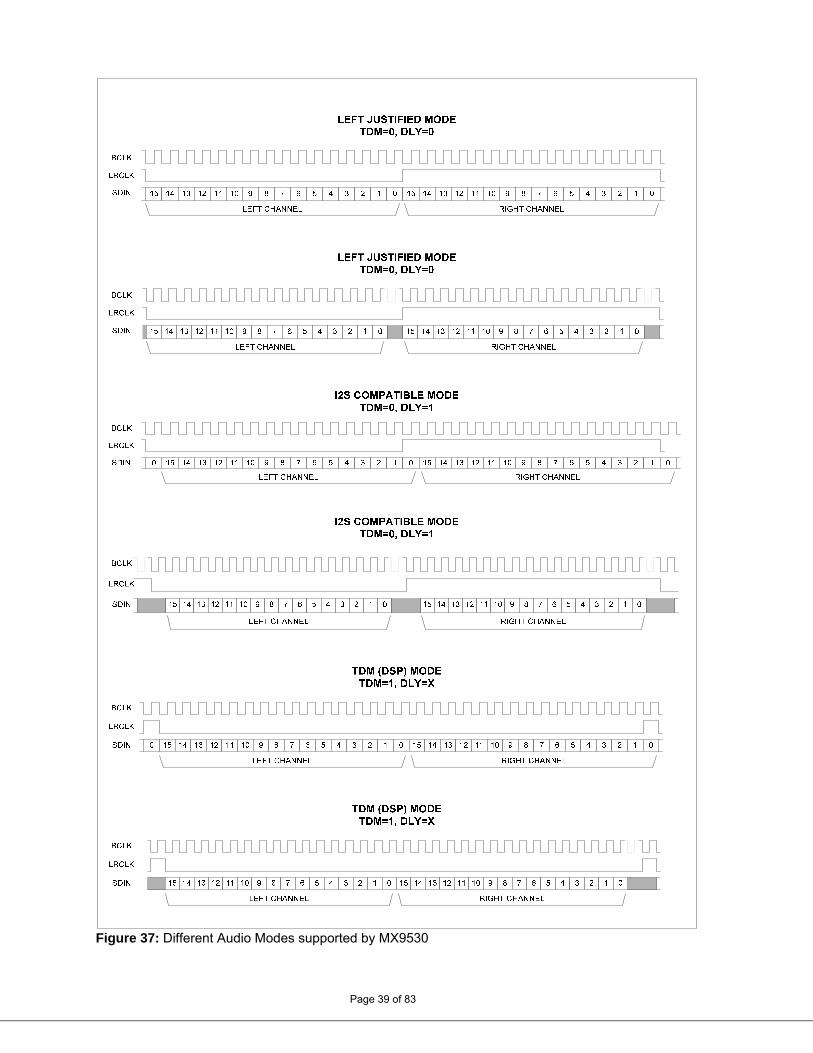
Figure 37: Different Audio Modes supported by MX9530
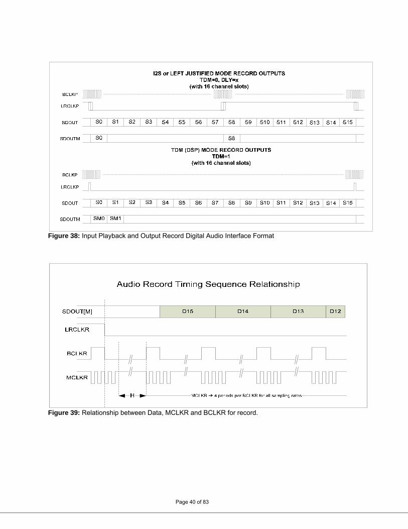
Figure 38: Input Playback and Output Record Digital Audio Interface Format
Figure 39: Relationship between Data, MCLKR and BCLKR for record.
Page 40 of 83
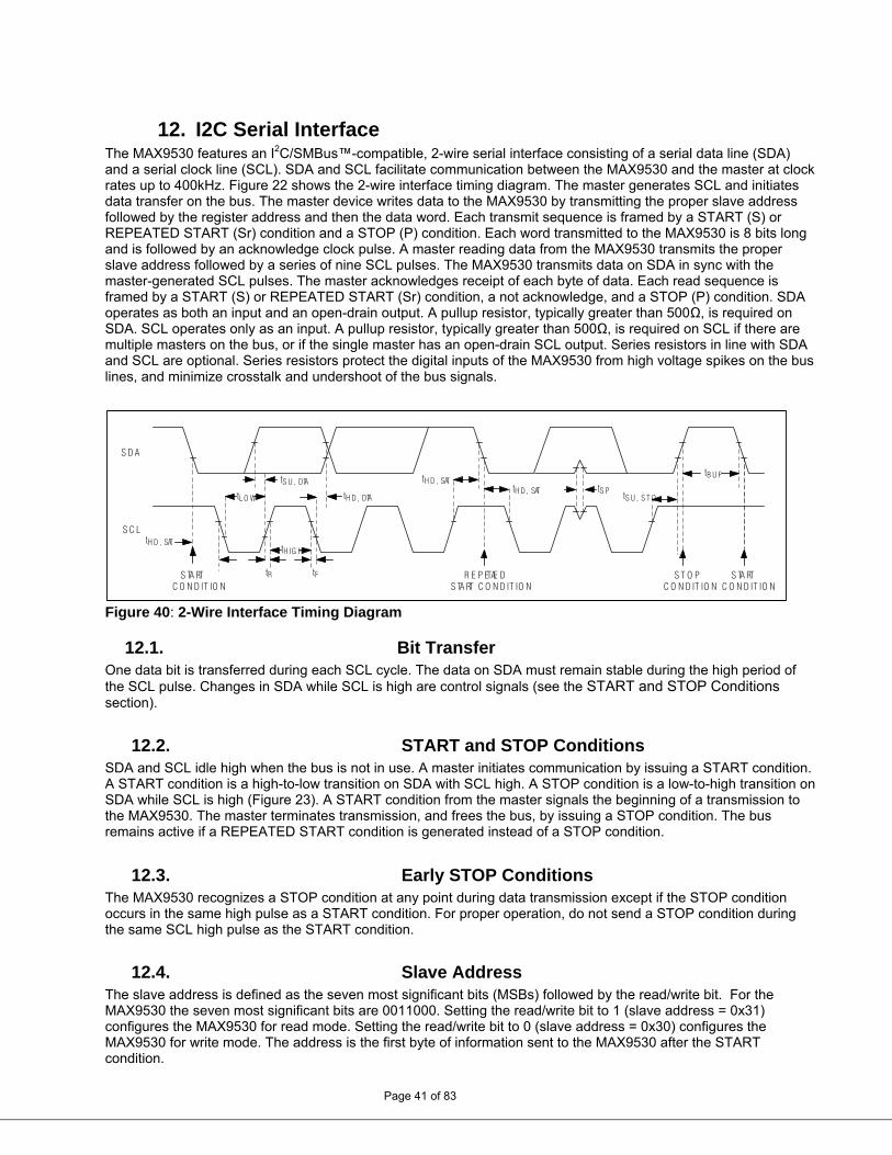
12. I2C Serial Interface The MAX9530 features an I2C/SMBus™-compatible, 2-wire serial interface consisting of a serial data line (SDA) and a serial clock line (SCL). SDA and SCL facilitate communication between the MAX9530 and the master at clock rates up to 400kHz. Figure 22 shows the 2-wire interface timing diagram. The master generates SCL and initiates data transfer on the bus. The master device writes data to the MAX9530 by transmitting the proper slave address followed by the register address and then the data word. Each transmit sequence is framed by a START (S) or REPEATED START (Sr) condition and a STOP (P) condition. Each word transmitted to the MAX9530 is 8 bits long and is followed by an acknowledge clock pulse. A master reading data from the MAX9530 transmits the proper slave address followed by a series of nine SCL pulses. The MAX9530 transmits data on SDA in sync with the master-generated SCL pulses. The master acknowledges receipt of each byte of data. Each read sequence is framed by a START (S) or REPEATED START (Sr) condition, a not acknowledge, and a STOP (P) condition. SDA operates as both an input and an open-drain output. A pullup resistor, typically greater than 500Ω, is required on SDA. SCL operates only as an input. A pullup resistor, typically greater than 500Ω, is required on SCL if there are multiple masters on the bus, or if the single master has an open-drain SCL output. Series resistors in line with SDA and SCL are optional. Series resistors protect the digital inputs of the MAX9530 from high voltage spikes on the bus lines, and minimize crosstalk and undershoot of the bus signals.
S C L
S D A
S TA RTC O N D IT IO N
S T O PC O N D IT IO N
R E P E AT E DS TA RT C O N D IT IO N
S TA RTC O N D IT IO N
tH D , S TA
tH D , S TAtH D , S TA tS P
tB U F
tS U , S T OtL O W
tS U , D AT
tH D , D AT
tH IG H
tR tF
Figure 40: 2-Wire Interface Timing Diagram
12.1. Bit Transfer One data bit is transferred during each SCL cycle. The data on SDA must remain stable during the high period of the SCL pulse. Changes in SDA while SCL is high are control signals (see the START and STOP Conditions section).
12.2. START and STOP Conditions SDA and SCL idle high when the bus is not in use. A master initiates communication by issuing a START condition. A START condition is a high-to-low transition on SDA with SCL high. A STOP condition is a low-to-high transition on SDA while SCL is high (Figure 23). A START condition from the master signals the beginning of a transmission to the MAX9530. The master terminates transmission, and frees the bus, by issuing a STOP condition. The bus remains active if a REPEATED START condition is generated instead of a STOP condition.
12.3. Early STOP Conditions The MAX9530 recognizes a STOP condition at any point during data transmission except if the STOP condition occurs in the same high pulse as a START condition. For proper operation, do not send a STOP condition during the same SCL high pulse as the START condition.
12.4. Slave Address
Page 41 of 83
The slave address is defined as the seven most significant bits (MSBs) followed by the read/write bit. For the MAX9530 the seven most significant bits are 0011000. Setting the read/write bit to 1 (slave address = 0x31) configures the MAX9530 for read mode. Setting the read/write bit to 0 (slave address = 0x30) configures the MAX9530 for write mode. The address is the first byte of information sent to the MAX9530 after the START condition.
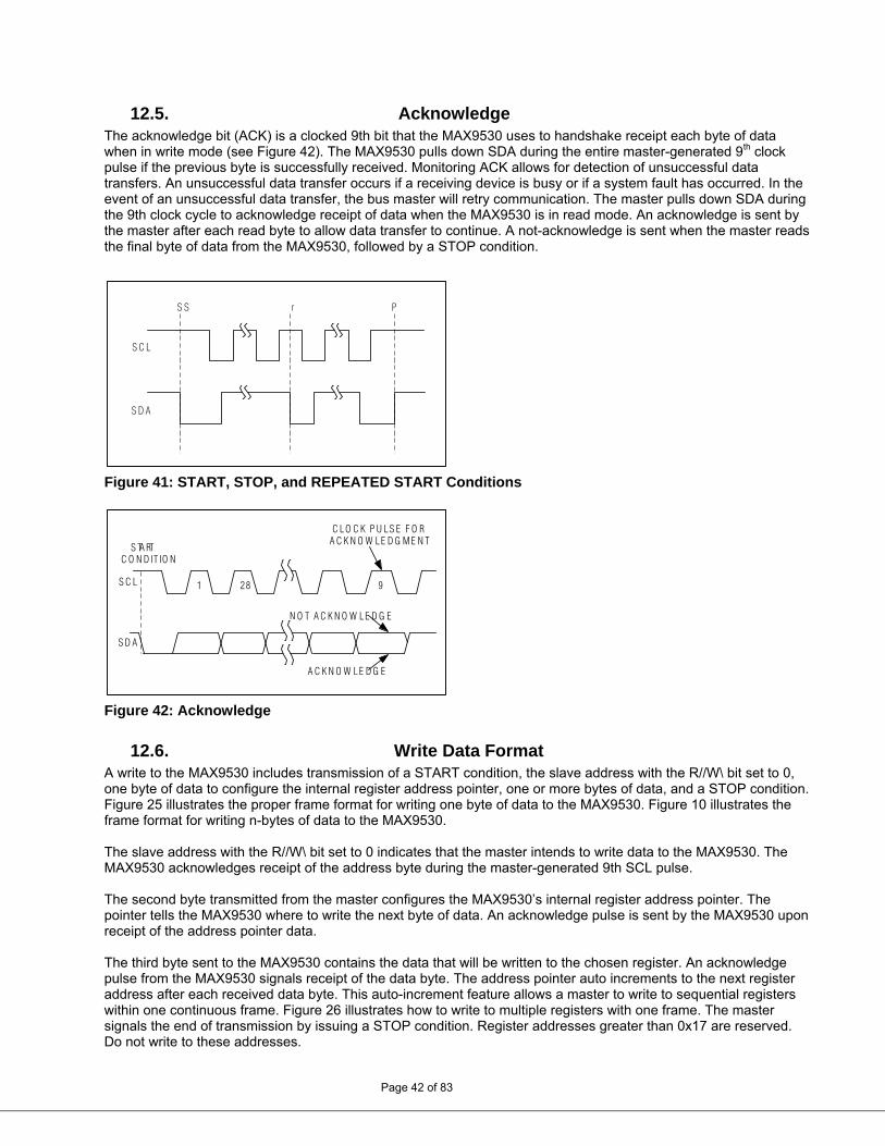
12.5. Acknowledge The acknowledge bit (ACK) is a clocked 9th bit that the MAX9530 uses to handshake receipt each byte of data when in write mode (see Figure 42). The MAX9530 pulls down SDA during the entire master-generated 9th clock pulse if the previous byte is successfully received. Monitoring ACK allows for detection of unsuccessful data transfers. An unsuccessful data transfer occurs if a receiving device is busy or if a system fault has occurred. In the event of an unsuccessful data transfer, the bus master will retry communication. The master pulls down SDA during the 9th clock cycle to acknowledge receipt of data when the MAX9530 is in read mode. An acknowledge is sent by the master after each read byte to allow data transfer to continue. A not-acknowledge is sent when the master reads the final byte of data from the MAX9530, followed by a STOP condition.
S C L
S D A
S S r P
Figure 41: START, STOP, and REPEATED START Conditions
1S C L
S TA RTC O N D IT IO N
S D A
28 9
C L O C K P U LS E F O RA C K N O W LE D G ME N T
A C K N O W LE D G E
N O T A C K N O W L E D G E
Figure 42: Acknowledge
12.6. Write Data Format A write to the MAX9530 includes transmission of a START condition, the slave address with the R//W\ bit set to 0, one byte of data to configure the internal register address pointer, one or more bytes of data, and a STOP condition. Figure 25 illustrates the proper frame format for writing one byte of data to the MAX9530. Figure 10 illustrates the frame format for writing n-bytes of data to the MAX9530. The slave address with the R//W\ bit set to 0 indicates that the master intends to write data to the MAX9530. The MAX9530 acknowledges receipt of the address byte during the master-generated 9th SCL pulse. The second byte transmitted from the master configures the MAX9530’s internal register address pointer. The pointer tells the MAX9530 where to write the next byte of data. An acknowledge pulse is sent by the MAX9530 upon receipt of the address pointer data.
Page 42 of 83
The third byte sent to the MAX9530 contains the data that will be written to the chosen register. An acknowledge pulse from the MAX9530 signals receipt of the data byte. The address pointer auto increments to the next register address after each received data byte. This auto-increment feature allows a master to write to sequential registers within one continuous frame. Figure 26 illustrates how to write to multiple registers with one frame. The master signals the end of transmission by issuing a STOP condition. Register addresses greater than 0x17 are reserved. Do not write to these addresses.
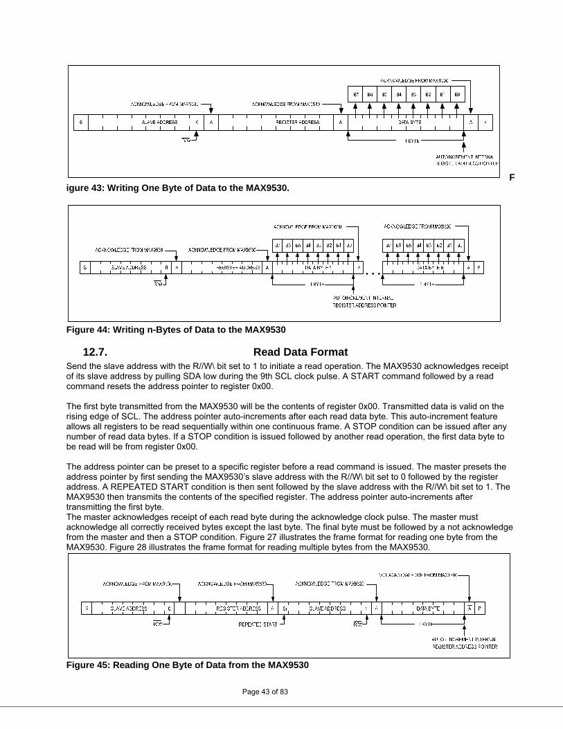
Figure 43: Writing One Byte of Data to the MAX9530.
Figure 44: Writing n-Bytes of Data to the MAX9530
12.7. Read Data Format Send the slave address with the R//W\ bit set to 1 to initiate a read operation. The MAX9530 acknowledges receipt of its slave address by pulling SDA low during the 9th SCL clock pulse. A START command followed by a read command resets the address pointer to register 0x00. The first byte transmitted from the MAX9530 will be the contents of register 0x00. Transmitted data is valid on the rising edge of SCL. The address pointer auto-increments after each read data byte. This auto-increment feature allows all registers to be read sequentially within one continuous frame. A STOP condition can be issued after any number of read data bytes. If a STOP condition is issued followed by another read operation, the first data byte to be read will be from register 0x00. The address pointer can be preset to a specific register before a read command is issued. The master presets the address pointer by first sending the MAX9530’s slave address with the R//W\ bit set to 0 followed by the register address. A REPEATED START condition is then sent followed by the slave address with the R//W\ bit set to 1. The MAX9530 then transmits the contents of the specified register. The address pointer auto-increments after transmitting the first byte. The master acknowledges receipt of each read byte during the acknowledge clock pulse. The master must acknowledge all correctly received bytes except the last byte. The final byte must be followed by a not acknowledge from the master and then a STOP condition. Figure 27 illustrates the frame format for reading one byte from the MAX9530. Figure 28 illustrates the frame format for reading multiple bytes from the MAX9530.
Page 43 of 83
Figure 45: Reading One Byte of Data from the MAX9530
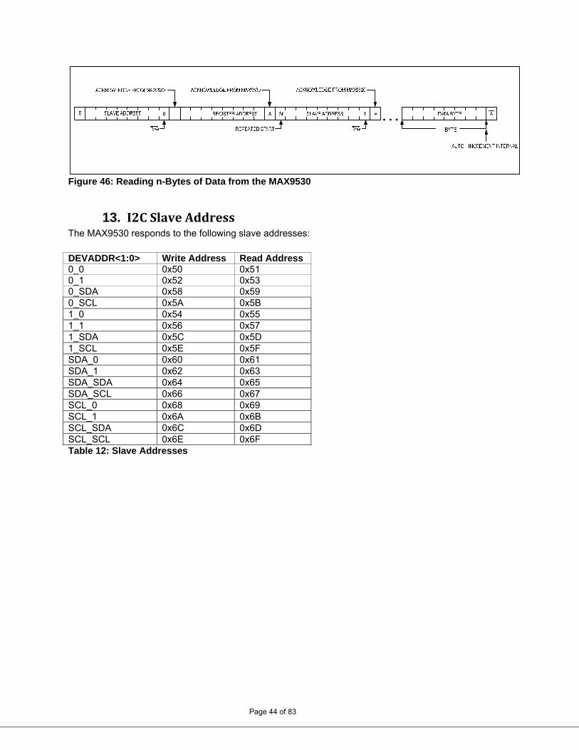
Figure 46: Reading n-Bytes of Data from the MAX9530
13. I2C Slave Address The MAX9530 responds to the following slave addresses:
DEVADDR<1:0> Write Address Read Address 0_0 0x50 0x51 0_1 0x52 0x53 0_SDA 0x58 0x59 0_SCL 0x5A 0x5B 1_0 0x54 0x55 1_1 0x56 0x57 1_SDA 0x5C 0x5D 1_SCL 0x5E 0x5F SDA_0 0x60 0x61 SDA_1 0x62 0x63 SDA_SDA 0x64 0x65 SDA_SCL 0x66 0x67 SCL_0 0x68 0x69 SCL_1 0x6A 0x6B SCL_SDA 0x6C 0x6D SCL_SCL 0x6E 0x6F
Page 44 of 83
Table 12: Slave Addresses
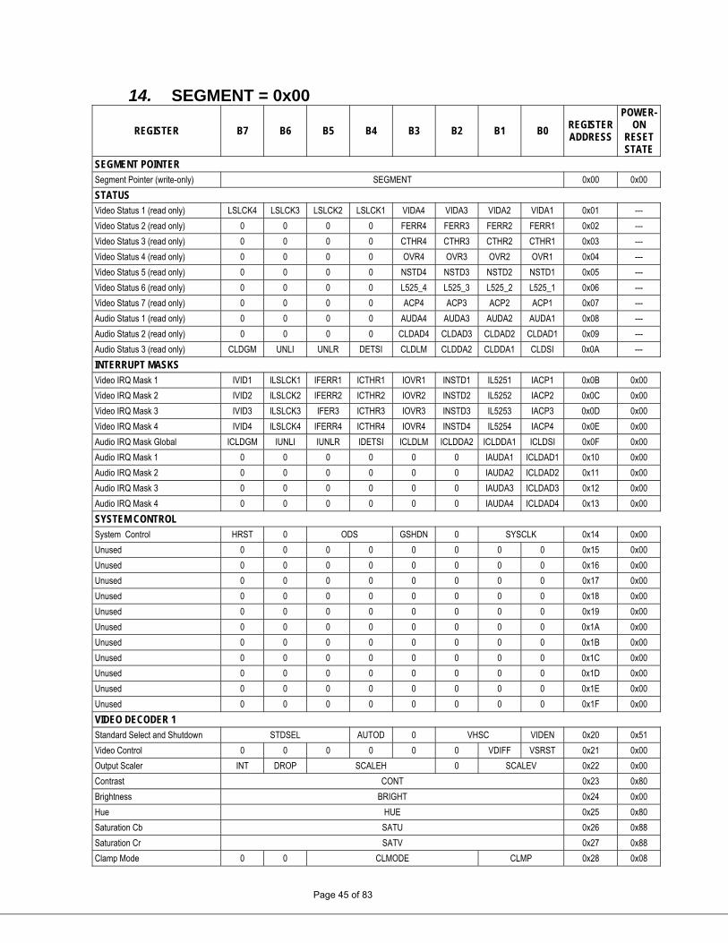
14. SEGMENT = 0x00
REGISTER B7 B6 B5 B4 B3 B2 B1 B0 REGISTER ADDRESS
POWER-ON
RESET STATE
SEGMENT POINTER Segment Pointer (write-only) SEGMENT 0x00 0x00
STATUS Video Status 1 (read only) LSLCK4 LSLCK3 LSLCK2 LSLCK1 VIDA4 VIDA3 VIDA2 VIDA1 0x01 ---
Video Status 2 (read only) 0 0 0 0 FERR4 FERR3 FERR2 FERR1 0x02 ---
Video Status 3 (read only) 0 0 0 0 CTHR4 CTHR3 CTHR2 CTHR1 0x03 ---
Video Status 4 (read only) 0 0 0 0 OVR4 OVR3 OVR2 OVR1 0x04 ---
Video Status 5 (read only) 0 0 0 0 NSTD4 NSTD3 NSTD2 NSTD1 0x05 ---
Video Status 6 (read only) 0 0 0 0 L525_4 L525_3 L525_2 L525_1 0x06 ---
Video Status 7 (read only) 0 0 0 0 ACP4 ACP3 ACP2 ACP1 0x07 ---
Audio Status 1 (read only) 0 0 0 0 AUDA4 AUDA3 AUDA2 AUDA1 0x08 ---
Audio Status 2 (read only) 0 0 0 0 CLDAD4 CLDAD3 CLDAD2 CLDAD1 0x09 ---
Audio Status 3 (read only) CLDGM UNLI UNLR DETSI CLDLM CLDDA2 CLDDA1 CLDSI 0x0A ---
INTERRUPT MASKS Video IRQ Mask 1 IVID1 ILSLCK1 IFERR1 ICTHR1 IOVR1 INSTD1 IL5251 IACP1 0x0B 0x00
Video IRQ Mask 2 IVID2 ILSLCK2 IFERR2 ICTHR2 IOVR2 INSTD2 IL5252 IACP2 0x0C 0x00
Video IRQ Mask 3 IVID3 ILSLCK3 IFER3 ICTHR3 IOVR3 INSTD3 IL5253 IACP3 0x0D 0x00
Video IRQ Mask 4 IVID4 ILSLCK4 IFERR4 ICTHR4 IOVR4 INSTD4 IL5254 IACP4 0x0E 0x00
Audio IRQ Mask Global ICLDGM IUNLI IUNLR IDETSI ICLDLM ICLDDA2 ICLDDA1 ICLDSI 0x0F 0x00
Audio IRQ Mask 1 0 0 0 0 0 0 IAUDA1 ICLDAD1 0x10 0x00
Audio IRQ Mask 2 0 0 0 0 0 0 IAUDA2 ICLDAD2 0x11 0x00
Audio IRQ Mask 3 0 0 0 0 0 0 IAUDA3 ICLDAD3 0x12 0x00
Audio IRQ Mask 4 0 0 0 0 0 0 IAUDA4 ICLDAD4 0x13 0x00
SYSTEM CONTROL System Control HRST 0 ODS GSHDN 0 SYSCLK 0x14 0x00
Unused 0 0 0 0 0 0 0 0 0x15 0x00
Unused 0 0 0 0 0 0 0 0 0x16 0x00
Unused 0 0 0 0 0 0 0 0 0x17 0x00
Unused 0 0 0 0 0 0 0 0 0x18 0x00
Unused 0 0 0 0 0 0 0 0 0x19 0x00
Unused 0 0 0 0 0 0 0 0 0x1A 0x00
Unused 0 0 0 0 0 0 0 0 0x1B 0x00
Unused 0 0 0 0 0 0 0 0 0x1C 0x00
Unused 0 0 0 0 0 0 0 0 0x1D 0x00
Unused 0 0 0 0 0 0 0 0 0x1E 0x00
Unused 0 0 0 0 0 0 0 0 0x1F 0x00
VIDEO DECODER 1 Standard Select and Shutdown STDSEL AUTOD 0 VHSC VIDEN 0x20 0x51
Video Control 0 0 0 0 0 0 VDIFF VSRST 0x21 0x00
Output Scaler INT DROP SCALEH 0 SCALEV 0x22 0x00
Contrast CONT 0x23 0x80
Brightness BRIGHT 0x24 0x00
Hue HUE 0x25 0x80
Saturation Cb SATU 0x26 0x88
Saturation Cr SATV 0x27 0x88
Clamp Mode 0 0 CLMODE
Page 45 of 83
CLMP 0x28 0x08
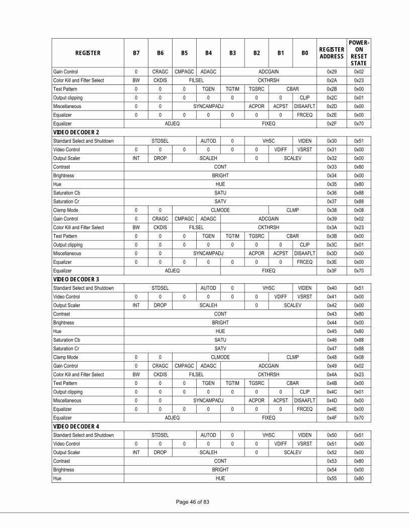
REGISTER B7 B6 B5 B4 B3 B2 B1 B0 REGISTER ADDRESS
POWER-ON
RESET STATE
Gain Control 0 CRAGC CMPAGC ADAGC ADCGAIN 0x29 0x02
Color Kill and Filter Select BW CKDIS FILSEL CKTHRSH 0x2A 0x23
Test Pattern 0 0 0 TGEN TGTIM TGSRC CBAR 0x2B 0x00
Output clipping 0 0 0 0 0 0 0 CLIP 0x2C 0x01
Miscellaneous 0 0 SYNCAMPADJ ACPOR ACPST DISAAFLT 0x2D 0x00
Equalizer 0 0 0 0 0 0 0 FRCEQ 0x2E 0x00
Equalizer ADJEQ FIXEQ 0x2F 0x70
VIDEO DECODER 2 Standard Select and Shutdown STDSEL AUTOD 0 VHSC VIDEN 0x30 0x51
Video Control 0 0 0 0 0 0 VDIFF VSRST 0x31 0x00
Output Scaler INT DROP SCALEH 0 SCALEV 0x32 0x00
Contrast CONT 0x33 0x80
Brightness BRIGHT 0x34 0x00
Hue HUE 0x35 0x80
Saturation Cb SATU 0x36 0x88
Saturation Cr SATV 0x37 0x88
Clamp Mode 0 0 CLMODE CLMP 0x38 0x08
Gain Control 0 CRAGC CMPAGC ADAGC ADCGAIN 0x39 0x02
Color Kill and Filter Select BW CKDIS FILSEL CKTHRSH 0x3A 0x23
Test Pattern 0 0 0 TGEN TGTIM TGSRC CBAR 0x3B 0x00
Output clipping 0 0 0 0 0 0 0 CLIP 0x3C 0x01
Miscellaneous 0 0 SYNCAMPADJ ACPOR ACPST DISAAFLT 0x3D 0x00
Equalizer 0 0 0 0 0 0 0 FRCEQ 0x3E 0x00
Equalizer ADJEQ FIXEQ 0x3F 0x70
VIDEO DECODER 3 Standard Select and Shutdown STDSEL AUTOD 0 VHSC VIDEN 0x40 0x51
Video Control 0 0 0 0 0 0 VDIFF VSRST 0x41 0x00
Output Scaler INT DROP SCALEH 0 SCALEV 0x42 0x00
Contrast CONT 0x43 0x80
Brightness BRIGHT 0x44 0x00
Hue HUE 0x45 0x80
Saturation Cb SATU 0x46 0x88
Saturation Cr SATV 0x47 0x88
Clamp Mode 0 0 CLMODE CLMP 0x48 0x08
Gain Control 0 CRAGC CMPAGC ADAGC ADCGAIN 0x49 0x02
Color Kill and Filter Select BW CKDIS FILSEL CKTHRSH 0x4A 0x23
Test Pattern 0 0 0 TGEN TGTIM TGSRC CBAR 0x4B 0x00
Output clipping 0 0 0 0 0 0 0 CLIP 0x4C 0x01
Miscellaneous 0 0 SYNCAMPADJ ACPOR ACPST DISAAFLT 0x4D 0x00
Equalizer 0 0 0 0 0 0 0 FRCEQ 0x4E 0x00
Equalizer ADJEQ FIXEQ 0x4F 0x70
VIDEO DECODER 4 Standard Select and Shutdown STDSEL AUTOD 0 VHSC VIDEN 0x50 0x51
Video Control 0 0 0 0 0 0 VDIFF VSRST 0x51 0x00
Output Scaler INT DROP SCALEH 0 SCALEV 0x52 0x00
Contrast CONT 0x53 0x80
Brightness BRIGHT 0x54 0x00
Hue
Page 46 of 83
HUE 0x55 0x80
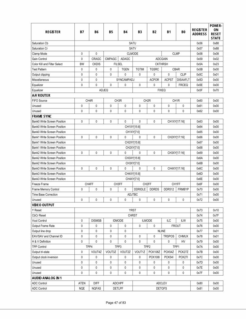
REGISTER B7 B6 B5 B4 B3 B2 B1 B0 REGISTER ADDRESS
POWER-ON
RESET STATE
Saturation Cb SATU 0x56 0x88
Saturation Cr SATV 0x57 0x88
Clamp Mode 0 0 CLMODE CLMP 0x58 0x08
Gain Control 0 CRAGC CMPAGC ADAGC ADCGAIN 0x59 0x02
Color Kill and Filter Select BW CKDIS FILSEL CKTHRSH 0x5A 0x23
Test Pattern 0 0 0 TGEN TGTIM TGSRC CBAR 0x5B 0x00
Output clipping 0 0 0 0 0 0 0 CLIP 0x5C 0x01
Miscellaneous 0 0 SYNCAMPADJ ACPOR ACPST DISAAFLT 0x5D 0x00
Equalizer 0 0 0 0 0 0 0 FRCEQ 0x5E 0x00
Equalizer ADJEQ FIXEQ 0x5F 0x70
A/V ROUTER FIFO Source CH4R CH3R CH2R CH1R 0x60 0x00
Unused 0 0 0 0 0 0 0 0 0x61 0x00
Unused 0 0 0 0 0 0 0 0 0x62 0x00
FRAME SYNC Bank0 Write Screen Position 0 0 0 0 0 0 CH1XY[17:16] 0x63 0x00
Bank0 Write Screen Position CH1XY[15:8] 0x64 0x00
Bank0 Write Screen Position CH1XY[7:0] 0x65 0x00
Bank1 Write Screen Position 0 0 0 0 0 0 CH2XY[17:16] 0x66 0x00
Bank1 Write Screen Position CH2XY[15:8] 0x67 0x00
Bank1 Write Screen Position CH2XY[7:0] 0x68 0x00
Bank2 Write Screen Position 0 0 0 0 0 0 CH3XY[17:16] 0x69 0x00
Bank2 Write Screen Position CH3XY[15:8] 0x6A 0x00
Bank2 Write Screen Position CH3XY[7:0] 0x6B 0x00
Bank3 Write Screen Position 0 0 0 0 0 0 CH4XY[17:16] 0x6C 0x00
Bank3 Write Screen Position CH4XY[15:8] 0x6D 0x00
Bank3 Write Screen Position CH4XY[7:0] 0x6E 0x00
Freeze Frame CH4FF CH3FF CH2FF CH1FF 0x6F 0x00
Frame Memory Control 0 0 0 0 DDRIDLE DDRDS DDR512 FRMBYP 0x70 0x00
Time Base Correction ADJTBC 0x71 0x00
Unused 0 0 0 0 0 0 0 0 0x72 0x00
VIDEO OUTPUT Y Reset YRST 0x73 0x10
CbCr Reset CHRST 0x74 0x7F
Vout Control 0 DISMSB IDMODE ILMODE ILC ILW 0x75 0x00
Output Frame Rate 0 0 0 0 0 0 FROUT 0x76 0x00
Output line drop 0 0 0 0 NLINE 0x77 0x01
EAV/SAV and Channel ID 0 0 0 0 0 0 TRSPOS CHMUX 0x78 0x01
H & V Definition 0 0 0 0 0 0 0 HV 0x79 0x00
TPP Control TPP4 TPP3 TPP2 TPP1 0x7A 0x00
Output tri-state 0 VOUT4Z VOUT3Z VOUT2Z VOUT1Z PCK108Z PCK54Z PCK27Z 0x7B 0x00
Output clock inversion 0 0 0 0 0 PCK108I PCK54I PCK27I 0x7C 0x00
Unused 0 0 0 0 0 0 0 0 0x7D 0x00
Unused 0 0 0 0 0 0 0 0 0x7E 0x00
Unused 0 0 0 0 0 0 0 0 0x7F 0x00
AUDIO ANALOG IN 1 ADC Control ATEN DIFF ADCHPF ADCLEV 0x80 0x00
ADC Control NQE NQFAS DETLPF
Page 47 of 83
DETOFS 0x81 0x00
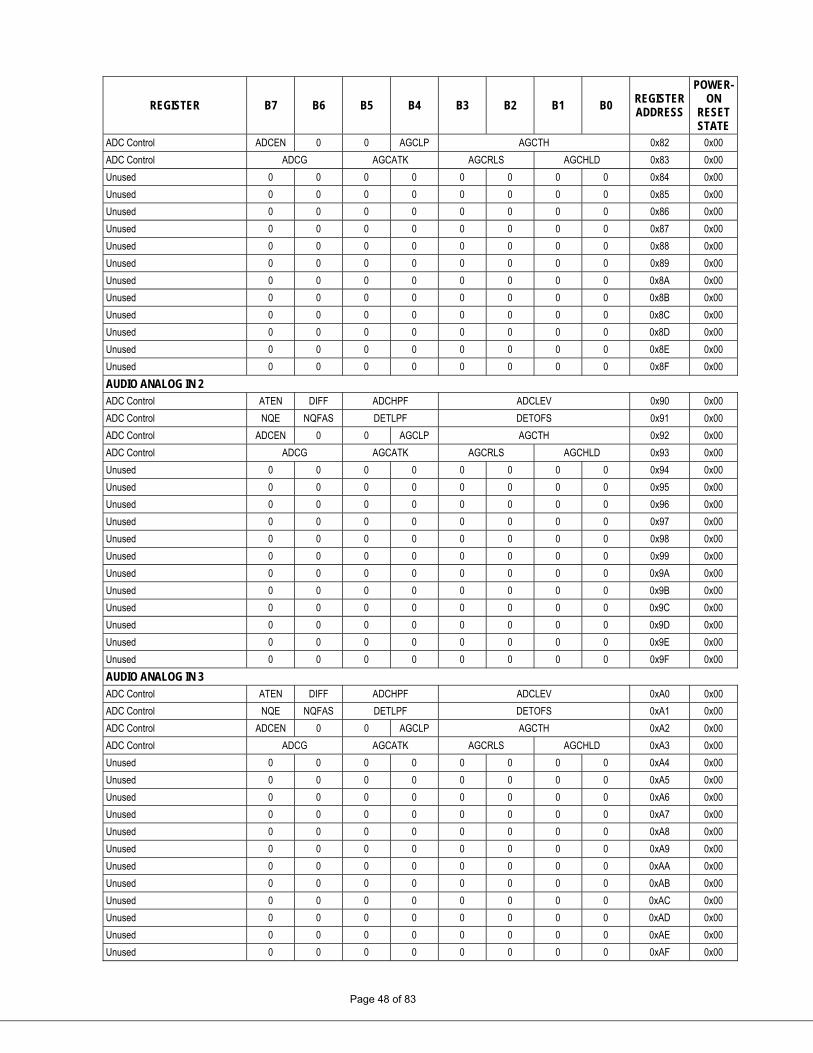
REGISTER B7 B6 B5 B4 B3 B2 B1 B0 REGISTER ADDRESS
POWER-ON
RESET STATE
ADC Control ADCEN 0 0 AGCLP AGCTH 0x82 0x00
ADC Control ADCG AGCATK AGCRLS AGCHLD 0x83 0x00
Unused 0 0 0 0 0 0 0 0 0x84 0x00
Unused 0 0 0 0 0 0 0 0 0x85 0x00
Unused 0 0 0 0 0 0 0 0 0x86 0x00
Unused 0 0 0 0 0 0 0 0 0x87 0x00
Unused 0 0 0 0 0 0 0 0 0x88 0x00
Unused 0 0 0 0 0 0 0 0 0x89 0x00
Unused 0 0 0 0 0 0 0 0 0x8A 0x00
Unused 0 0 0 0 0 0 0 0 0x8B 0x00
Unused 0 0 0 0 0 0 0 0 0x8C 0x00
Unused 0 0 0 0 0 0 0 0 0x8D 0x00
Unused 0 0 0 0 0 0 0 0 0x8E 0x00
Unused 0 0 0 0 0 0 0 0 0x8F 0x00
AUDIO ANALOG IN 2 ADC Control ATEN DIFF ADCHPF ADCLEV 0x90 0x00
ADC Control NQE NQFAS DETLPF DETOFS 0x91 0x00
ADC Control ADCEN 0 0 AGCLP AGCTH 0x92 0x00
ADC Control ADCG AGCATK AGCRLS AGCHLD 0x93 0x00
Unused 0 0 0 0 0 0 0 0 0x94 0x00
Unused 0 0 0 0 0 0 0 0 0x95 0x00
Unused 0 0 0 0 0 0 0 0 0x96 0x00
Unused 0 0 0 0 0 0 0 0 0x97 0x00
Unused 0 0 0 0 0 0 0 0 0x98 0x00
Unused 0 0 0 0 0 0 0 0 0x99 0x00
Unused 0 0 0 0 0 0 0 0 0x9A 0x00
Unused 0 0 0 0 0 0 0 0 0x9B 0x00
Unused 0 0 0 0 0 0 0 0 0x9C 0x00
Unused 0 0 0 0 0 0 0 0 0x9D 0x00
Unused 0 0 0 0 0 0 0 0 0x9E 0x00
Unused 0 0 0 0 0 0 0 0 0x9F 0x00
AUDIO ANALOG IN 3 ADC Control ATEN DIFF ADCHPF ADCLEV 0xA0 0x00
ADC Control NQE NQFAS DETLPF DETOFS 0xA1 0x00
ADC Control ADCEN 0 0 AGCLP AGCTH 0xA2 0x00
ADC Control ADCG AGCATK AGCRLS AGCHLD 0xA3 0x00
Unused 0 0 0 0 0 0 0 0 0xA4 0x00
Unused 0 0 0 0 0 0 0 0 0xA5 0x00
Unused 0 0 0 0 0 0 0 0 0xA6 0x00
Unused 0 0 0 0 0 0 0 0 0xA7 0x00
Unused 0 0 0 0 0 0 0 0 0xA8 0x00
Unused 0 0 0 0 0 0 0 0 0xA9 0x00
Unused 0 0 0 0 0 0 0 0 0xAA 0x00
Unused 0 0 0 0 0 0 0 0 0xAB 0x00
Unused 0 0 0 0 0 0 0 0 0xAC 0x00
Unused 0 0 0 0 0 0 0 0 0xAD 0x00
Unused 0 0 0 0 0 0 0 0 0xAE 0x00
Unused 0 0 0 0 0 0 0
Page 48 of 83
0 0xAF 0x00

REGISTER B7 B6 B5 B4 B3 B2 B1 B0 REGISTER ADDRESS
POWER-ON
RESET STATE
AUDIO ANALOG IN 4 ADC Control ATEN DIFF ADCHPF ADCLEV 0xB0 0x00
ADC Control NQE NQFAS DETLPF DETOFS 0xB1 0x00
ADC Control ADCEN 0 0 AGCLP AGCTH 0xB2 0x00
ADC Control ADCG AGCATK AGCRLS AGCHLD 0xB3 0x00
Unused 0 0 0 0 0 0 0 0 0xB4 0x00
Unused 0 0 0 0 0 0 0 0 0xB5 0x00
Unused 0 0 0 0 0 0 0 0 0xB6 0x00
Unused 0 0 0 0 0 0 0 0 0xB7 0x00
Unused 0 0 0 0 0 0 0 0 0xB8 0x00
Unused 0 0 0 0 0 0 0 0 0xB9 0x00
Unused 0 0 0 0 0 0 0 0 0xBA 0x00
Unused 0 0 0 0 0 0 0 0 0xBB 0x00
Unused 0 0 0 0 0 0 0 0 0xBC 0x00
Unused 0 0 0 0 0 0 0 0 0xBD 0x00
Unused 0 0 0 0 0 0 0 0 0xBE 0x00
Unused 0 0 0 0 0 0 0 0 0xBF 0x00
AUDIO DIGITAL IN Serial Input IHPF ILENA IRENA DIEN IFREQ 0xC0 0x00
Serial Input 0 0 0 ILEVEL 0xC1 0x00
Serial Input IMAS 0 ITDM IBCI IDLY IBS 0xC2 0x00
AUDIO MIXERS Mixer 1 AMEN BMEN CMEN DMEN MIG0 0xC3 0x00
Mixer 1 MIG2 MIG1 0xC4 0x00
Mixer 1 MIG4 MIG3 0xC5 0x00
AUDIO DIGITAL OUT Serial Output ALSEL M0SEL 0xC6 0x00
Serial Output SMENA SOENA 0 M1SEL 0xC7 0x00
Serial Output AD2SLOT AD1SLOT 0xC8 0x00
Serial Output AD4SLOT AD3SLOT 0xC9 0x00
Serial Output SMHIZD SM8 SMFMT SOHIZD SO8 SOFMT 0xCA 0x00
Serial Output RMAS 0 RTDM RBCI RDLY RBS 0xCB 0x00
Unused 0 0 0 0 0 0 0 0 0xCC 0x00
Unused 0 0 0 0 0 0 0 0 0xCD 0x00
Unused 0 0 0 0 0 0 0 0 0xCE 0x00
Unused 0 0 0 0 0 0 0 0 0xCF 0x00
AUDIO ANALOG OUT Audio Out 1 DAC1HPF DAC1EN DAC1SEL 0xD0 0x00
Audio Out 1 DAC1INLEV 0xD1 0x00
Audio Out 1 DAC1MIXLEV 0xD2 0x00
Audio Out 2 DAC2HPF DAC2EN DAC2SEL 0xD3 0x00
Audio Out 2 DAC2INLEV 0xD4 0x00
Audio Out 2 DAC2MIXLEV 0xD5 0x00
AUDIO CONTROL Audio Global Enable 0 0 0 0 0 0 0 AUDEN 0xD6 0x00
AUDIO CLOCKS Audio Clock Control ALMAS ALENA IDNUM 0 AFREQ 0xD7 0x00
Unused 0 0 0 0 0 0 0
Page 49 of 83
0 0xD8 0x00
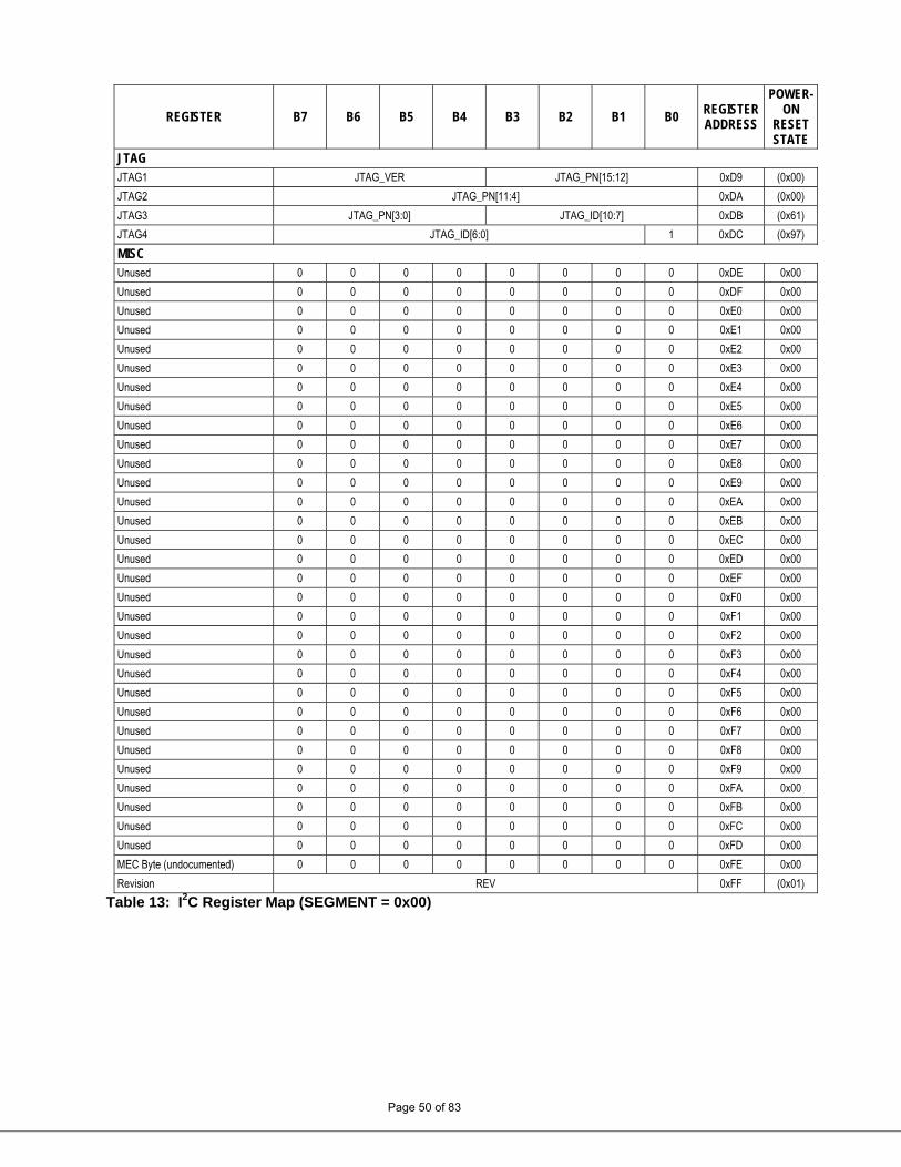
REGISTER B7 B6 B5 B4 B3 B2 B1 B0 REGISTER ADDRESS
POWER-ON
RESET STATE
JTAG JTAG1 JTAG_VER JTAG_PN[15:12] 0xD9 (0x00)
JTAG2 JTAG_PN[11:4] 0xDA (0x00)
JTAG3 JTAG_PN[3:0] JTAG_ID[10:7] 0xDB (0x61)
JTAG4 JTAG_ID[6:0] 1 0xDC (0x97)
MISC Unused 0 0 0 0 0 0 0 0 0xDE 0x00
Unused 0 0 0 0 0 0 0 0 0xDF 0x00
Unused 0 0 0 0 0 0 0 0 0xE0 0x00
Unused 0 0 0 0 0 0 0 0 0xE1 0x00
Unused 0 0 0 0 0 0 0 0 0xE2 0x00
Unused 0 0 0 0 0 0 0 0 0xE3 0x00
Unused 0 0 0 0 0 0 0 0 0xE4 0x00
Unused 0 0 0 0 0 0 0 0 0xE5 0x00
Unused 0 0 0 0 0 0 0 0 0xE6 0x00
Unused 0 0 0 0 0 0 0 0 0xE7 0x00
Unused 0 0 0 0 0 0 0 0 0xE8 0x00
Unused 0 0 0 0 0 0 0 0 0xE9 0x00
Unused 0 0 0 0 0 0 0 0 0xEA 0x00
Unused 0 0 0 0 0 0 0 0 0xEB 0x00
Unused 0 0 0 0 0 0 0 0 0xEC 0x00
Unused 0 0 0 0 0 0 0 0 0xED 0x00
Unused 0 0 0 0 0 0 0 0 0xEF 0x00
Unused 0 0 0 0 0 0 0 0 0xF0 0x00
Unused 0 0 0 0 0 0 0 0 0xF1 0x00
Unused 0 0 0 0 0 0 0 0 0xF2 0x00
Unused 0 0 0 0 0 0 0 0 0xF3 0x00
Unused 0 0 0 0 0 0 0 0 0xF4 0x00
Unused 0 0 0 0 0 0 0 0 0xF5 0x00
Unused 0 0 0 0 0 0 0 0 0xF6 0x00
Unused 0 0 0 0 0 0 0 0 0xF7 0x00
Unused 0 0 0 0 0 0 0 0 0xF8 0x00
Unused 0 0 0 0 0 0 0 0 0xF9 0x00
Unused 0 0 0 0 0 0 0 0 0xFA 0x00
Unused 0 0 0 0 0 0 0 0 0xFB 0x00
Unused 0 0 0 0 0 0 0 0 0xFC 0x00
Unused 0 0 0 0 0 0 0 0 0xFD 0x00
MEC Byte (undocumented) 0 0 0 0 0 0 0 0 0xFE 0x00
Revision REV 0xFF (0x01)
Page 50 of 83
Table 13: I2C Register Map (SEGMENT = 0x00)
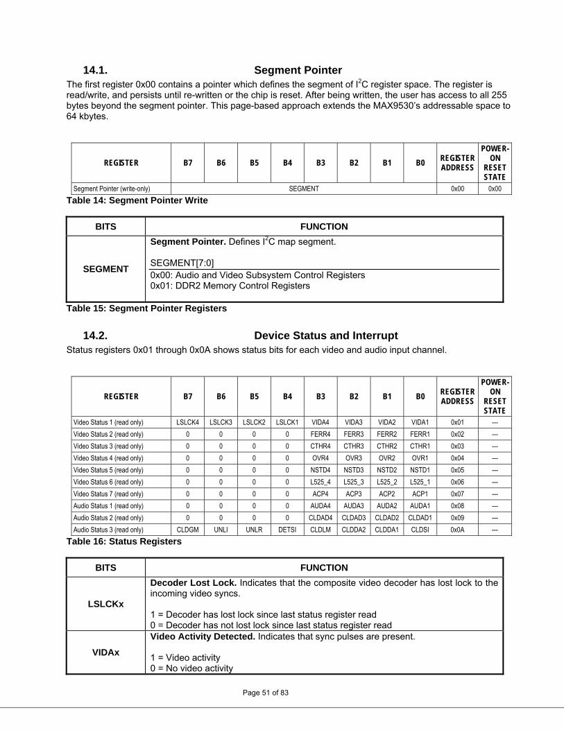
14.1. Segment Pointer
The first register 0x00 contains a pointer which defines the segment of I2C register space. The register is read/write, and persists until re-written or the chip is reset. After being written, the user has access to all 255 bytes beyond the segment pointer. This page-based approach extends the MAX9530’s addressable space to 64 kbytes.
REGISTER B7 B6 B5 B4 B3 B2 B0 REGISTER ADDRESS
POWER-ON
RESET STATE
B1
Segment Pointer (write-only) SEGMENT 0x00 0x00
Table 14: Segment Pointer Write
BITS FUNCTION
SEGMENT
Segment Pointer. Defines I2C map segment. SEGMENT[7:0] 0x00: Audio and Video Subsystem Control Registers 0x01: DDR2 Memory Control Registers
Table 15: Segment Pointer Registers
14.2. Device Status and Interrupt Status registers 0x01 through 0x0A shows status bits for each video and audio input channel.
REGISTER B7 B6 B5 B4 B3 B2 B1 B0 REGISTER ADDRESS
POWER-ON
RESET STATE
Video Status 1 (read only) LSLCK4 LSLCK3 LSLCK2 LSLCK1 VIDA4 VIDA3 VIDA2 VIDA1 0x01 ---
Video Status 2 (read only) 0 0 0 0 FERR4 FERR3 FERR2 FERR1 0x02 ---
Video Status 3 (read only) 0 0 0 0 CTHR4 CTHR3 CTHR2 CTHR1 0x03 ---
Video Status 4 (read only) 0 0 0 0 OVR4 OVR3 OVR2 OVR1 0x04 ---
Video Status 5 (read only) 0 0 0 0 NSTD4 NSTD3 NSTD2 NSTD1 0x05 ---
Video Status 6 (read only) 0 0 0 0 L525_4 L525_3 L525_2 L525_1 0x06 ---
Video Status 7 (read only) 0 0 0 0 ACP4 ACP3 ACP2 ACP1 0x07 ---
Audio Status 1 (read only) 0 0 0 0 AUDA4 AUDA3 AUDA2 AUDA1 0x08 ---
Audio Status 2 (read only) 0 0 0 0 CLDAD4 CLDAD3 CLDAD2 CLDAD1 0x09 ---
Audio Status 3 (read only) CLDGM UNLI UNLR DETSI CLDLM CLDDA2 CLDDA1 CLDSI 0x0A ---
Table 16: Status Registers
BITS FUNCTION
LSLCKx
Decoder Lost Lock. Indicates that the composite video decoder has lost lock to the incoming video syncs. 1 = Decoder has lost lock since last status register read 0 = Decoder has not lost lock since last status register read
VIDAx
Video Activity Detected. Indicates that sync pulses are present.
Page 51 of 83
1 = Video activity 0 = No video activity
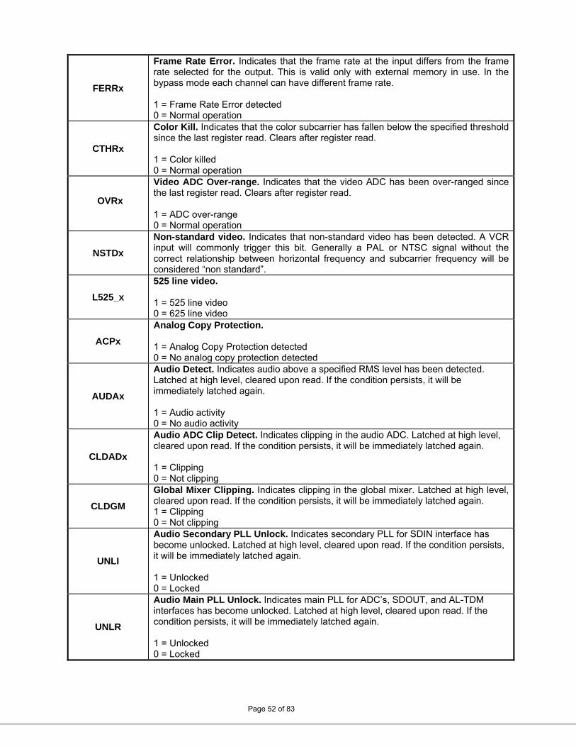
Frame Rate Error. Indicates that the frame rate at the input differs from the frame rate selected for the output. This is valid only with external memory in use. In the bypass mode each channel can have different frame rate.
FERRx 1 = Frame Rate Error detected 0 = Normal operation
CTHRx
Color Kill. Indicates that the color subcarrier has fallen below the specified threshold since the last register read. Clears after register read. 1 = Color killed 0 = Normal operation
OVRx
Video ADC Over-range. Indicates that the video ADC has been over-ranged since the last register read. Clears after register read. 1 = ADC over-range 0 = Normal operation
NSTDx
Non-standard video. Indicates that non-standard video has been detected. A VCR input will commonly trigger this bit. Generally a PAL or NTSC signal without the correct relationship between horizontal frequency and subcarrier frequency will be considered “non standard”.
L525_x
525 line video. 1 = 525 line video 0 = 625 line video
ACPx
Analog Copy Protection. 1 = Analog Copy Protection detected 0 = No analog copy protection detected
AUDAx
Audio Detect. Indicates audio above a specified RMS level has been detected. Latched at high level, cleared upon read. If the condition persists, it will be immediately latched again. 1 = Audio activity 0 = No audio activity
CLDADx
Audio ADC Clip Detect. Indicates clipping in the audio ADC. Latched at high level, cleared upon read. If the condition persists, it will be immediately latched again. 1 = Clipping 0 = Not clipping
CLDGM
Global Mixer Clipping. Indicates clipping in the global mixer. Latched at high level, cleared upon read. If the condition persists, it will be immediately latched again. 1 = Clipping 0 = Not clipping
UNLI
Audio Secondary PLL Unlock. Indicates secondary PLL for SDIN interface has become unlocked. Latched at high level, cleared upon read. If the condition persists, it will be immediately latched again. 1 = Unlocked 0 = Locked
UNLR
Audio Main PLL Unlock. Indicates main PLL for ADC’s, SDOUT, and AL-TDM interfaces has become unlocked. Latched at high level, cleared upon read. If the condition persists, it will be immediately latched again.
Page 52 of 83
1 = Unlocked 0 = Locked
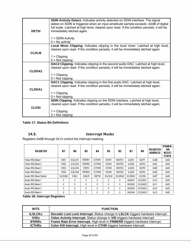
SDIN Activity Detect. Indicates activity detected on SDIN interface. The signal detect on SDIN is triggered when an input amplitude sample exceeds -42dB of digital full scale. Latched at high level, cleared upon read. If the condition persists, it will be immediately latched again. DETSI 1 = SDIN Activity 0 = No activity
CLDLM
Local Mixer Clipping. Indicates clipping in the local mixer. Latched at high level, cleared upon read. If the condition persists, it will be immediately latched again. 1 = Clipping 0 = Not clipping
CLDDA2
DAC2 Clipping. Indicates clipping in the second audio DAC. Latched at high level, cleared upon read. If the condition persists, it will be immediately latched again. 1 = Clipping 0 = Not clipping
CLDDA1
DAC1 Clipping. Indicates clipping in the first audio DAC. Latched at high level, cleared upon read. If the condition persists, it will be immediately latched again. 1 = Clipping 0 = Not clipping
CLDSI
SDIN Clipping. Indicates clipping on the SDIN interface. Latched at high level, cleared upon read. If the condition persists, it will be immediately latched again. 1 = Clipping 0 = Not clipping
Table 17: Status Bit Definitions
14.3. Interrupt Masks Registers 0x0B through 0x13 control the interrupt masking.
REGISTER B7 B5 B4 B3 B2 B6 B1 B0 REGISTER ADDRESS
POWER-ON
RESET STATE
Video IRQ Mask 1 IVID1 ILSLCK1 IFERR1 ICTHR1 IOVR1 INSTD1 IL5251 IACP1 0x0B 0x00
Video IRQ Mask 2 IVID2 ILSLCK2 IFERR2 ICTHR2 IOVR2 INSTD2 IL5252 IACP2 0x0C 0x00
Video IRQ Mask 3 IVID3 ILSLCK3 IFER3 ICTHR3 IOVR3 INSTD3 IL5253 IACP3 0x0D 0x00
Video IRQ Mask 4 IVID4 ILSLCK4 IFERR4 ICTHR4 IOVR4 INSTD4 IL5254 IACP4 0x0E 0x00
Audio IRQ Mask Global ICLDGM IUNLI IUNLR IDETSI ICLDLM ICLDDA2 ICLDDA1 ICLDSI 0x0F 0x00
Audio IRQ Mask 1 0 0 0 0 0 0 IAUDA1 ICLDAD1 0x10 0x00
Audio IRQ Mask 2 0 0 0 0 0 0 IAUDA2 ICLDAD2 0x11 0x00
Audio IRQ Mask 3 0 0 0 0 0 0 IAUDA3 ICLDAD3 0x12 0x00
Audio IRQ Mask 4 0 0 0 0 0 0 IAUDA4 ICLDAD4 0x13 0x00
Table 18: Interrupt Registers
BITS FUNCTION
Decoder Lost Lock Interrupt. Status change in LSLCK triggers hardware interrupt. ILSLCKx Video Activity Interrupt. Status change in VID triggers hardware interrupt. IVIDx Frame Rate Error Interrupt. High level in FRMERR triggers hardware interrupt. IFERRx
ICTHRx
Page 53 of 83
Color Kill Interrupt. High level in CTHR triggers hardware interrupt.
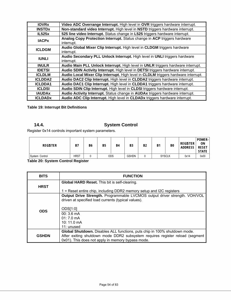
Video ADC Overrange Interrupt. High level in OVR triggers hardware interrupt. IOVRx Non-standard video Interrupt. High level in NSTD triggers hardware interrupt. INSTDx 525 line video Interrupt. Status change in L525 triggers hardware interrupt. IL525x Analog Copy Protection Interrupt. Status change in ACP triggers hardware interrupt.
IACPx
Audio Global Mixer Clip Interrupt. High level in CLDGM triggers hardware interrupt.
ICLDGM
Audio Secondary PLL Unlock Interrupt. High level in UNLI triggers hardware interrupt.
IUNLI
Audio Main PLL Unlock Interrupt. High level in UNLR triggers hardware interrupt. INULR Audio SDIN Activity Interrupt. High level in DETSI triggers hardware interrupt. IDETSI Audio Local Mixer Clip Interrupt. High level in CLDLM triggers hardware interrupt. ICLDLM Audio DAC2 Clip Interrupt. High level in CLDDA2 triggers hardware interrupt. ICLDDA2 Audio DAC1 Clip Interrupt. High level in CLDDA1 triggers hardware interrupt. ICLDDA1 Audio SDIN Clip Interrupt. High level in CLDSI triggers hardware interrupt. ICLDSI Audio Activity Interrupt. Status change in AUDAx triggers hardware interrupt. IAUDAx Audio ADC Clip Interrupt. High level in CLDADx triggers hardware interrupt. ICLDADx
Table 19: Interrupt Bit Definitions
14.4. System Control Register 0x14 controls important system parameters.
REGISTER B7 B6 B5 B4 B3 B2 B1 B0 REGISTER ADDRESS
POWER-ON
RESET STATE
System Control HRST 0 ODS GSHDN 0 SYSCLK 0x14 0x00
Table 20: System Control Register
BITS FUNCTION
HRST Global HARD Reset. This bit is self-clearing. 1 = Reset entire chip, including DDR2 memory setup and I2C registers
ODS
Output Drive Strength. Programmable LVCMOS output driver strength. VOH/VOL driven at specified load currents (typical values). ODS[1:0] 00: 3.6 mA
Page 54 of 83
01: 7.0 mA 10: 11.0 mA 11: unused
GSHDN Global Shutdown. Disables ALL functions, puts chip in 100% shutdown mode. After exiting shutdown mode DDR2 subsystem requires register reload (segment 0x01). This does not apply in memory bypass mode.
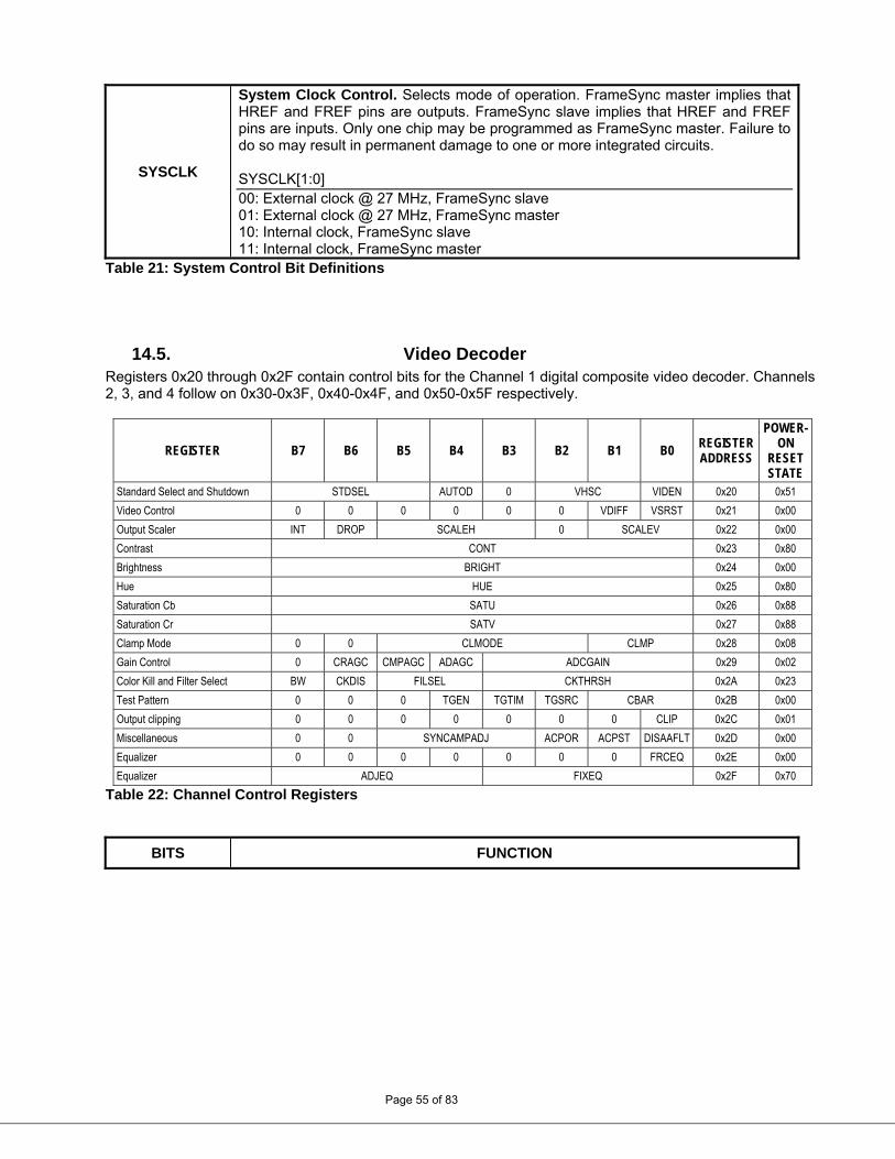
SYSCLK
System Clock Control. Selects mode of operation. FrameSync master implies that HREF and FREF pins are outputs. FrameSync slave implies that HREF and FREF pins are inputs. Only one chip may be programmed as FrameSync master. Failure to do so may result in permanent damage to one or more integrated circuits. SYSCLK[1:0] 00: External clock @ 27 MHz, FrameSync slave 01: External clock @ 27 MHz, FrameSync master 10: Internal clock, FrameSync slave 11: Internal clock, FrameSync master
Table 21: System Control Bit Definitions
14.5. Video Decoder Registers 0x20 through 0x2F contain control bits for the Channel 1 digital composite video decoder. Channels 2, 3, and 4 follow on 0x30-0x3F, 0x40-0x4F, and 0x50-0x5F respectively.
REGISTER B7 B6 B5 B4 B3 B2 B1 B0 REGISTER ADDRESS
POWER-ON
RESET STATE
Standard Select and Shutdown STDSEL AUTOD 0 VHSC VIDEN 0x20 0x51
Video Control 0 0 0 0 0 0 VDIFF VSRST 0x21 0x00
Output Scaler INT DROP SCALEH 0 SCALEV 0x22 0x00
Contrast CONT 0x23 0x80
Brightness BRIGHT 0x24 0x00
Hue HUE 0x25 0x80
Saturation Cb SATU 0x26 0x88
Saturation Cr SATV 0x27 0x88
Clamp Mode 0 0 CLMODE CLMP 0x28 0x08
Gain Control 0 CRAGC CMPAGC ADAGC ADCGAIN 0x29 0x02
Color Kill and Filter Select BW CKDIS FILSEL CKTHRSH 0x2A 0x23
Test Pattern 0 0 0 TGEN TGTIM TGSRC CBAR 0x2B 0x00
Output clipping 0 0 0 0 0 0 0 CLIP 0x2C 0x01
Miscellaneous 0 0 SYNCAMPADJ ACPOR ACPST DISAAFLT 0x2D 0x00
Equalizer 0 0 0 0 0 0 0 FRCEQ 0x2E 0x00
Equalizer ADJEQ FIXEQ 0x2F 0x70
Table 22: Channel Control Registers
Page 55 of 83
BITS FUNCTION
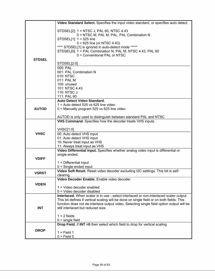
STDSEL
Video Standard Select. Specifies the input video standard, or specifies auto detect. STDSEL[2]: 1 = NTSC J, PAL 60, NTSC 4.43 0 = NTSC M, PAL M, PAL, PAL Combination N STDSEL[1]: 1 = 525 line 0 = 625 line (or NTSC 4.43) **** STDSEL[1] is ignored in auto-detect mode ***** STDSEL[0]: 1 = PAL Combination N, PAL M, NTSC 4.43, PAL 60 0 = Conventional PAL or NTSC STDSEL[2:0] 000: PAL 001: PAL Combination N 010: NTSC 011: PAL M 100: unused 101: NTSC 4.43 110: NTSC J 111: PAL 60
AUTOD
Auto Detect Video Standard. 1 = Auto detect 525 vs 625 line video 0 = Manually program 525 vs 625 line video AUTOD is only used to distinguish between standard PAL and NTSC
VHSC
VHS Command. Specifies how the decoder treats VHS inputs. VHSC[1:0] 00: Auto detect VHS input 01: Auto detect VHS input 10: Never treat input as VHS 11: Always treat input as VHS
VDIFF
Video Differential Input. Specifies whether analog video input is differential or single-ended. 1 = Differential input 0 = Single ended input
VSRST Video Soft Reset. Reset video decoder excluding I2C settings. This bit is self-clearing.
VIDEN
Video Decoder Enable. Enable video decoder. 1 = Video decoder enabled 0 = Video decoder disabled
INT
Interlaced. When scaler is in use - select interlaced or non-interlaced scaler output. This bit defines if vertical scaling will be done on single field or on both fields. This function does not de-interlace output video. Selecting single field option output will be still interlaced but reduced size. 1 = 2 fields 0 = single field
DROP
Drop Field. If INT =0 then select which field to drop for vertical scaling.
Page 56 of 83
1 = Field 1 0 = Field 0
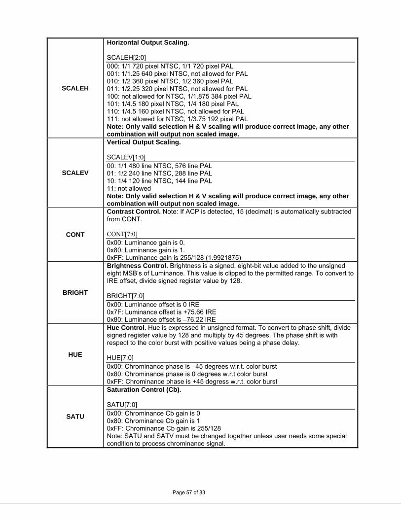
SCALEH
Horizontal Output Scaling. SCALEH[2:0] 000: 1/1 720 pixel NTSC, 1/1 720 pixel PAL 001: 1/1.25 640 pixel NTSC, not allowed for PAL 010: 1/2 360 pixel NTSC, 1/2 360 pixel PAL 011: 1/2.25 320 pixel NTSC, not allowed for PAL 100: not allowed for NTSC, 1/1.875 384 pixel PAL 101: 1/4.5 180 pixel NTSC, 1/4 180 pixel PAL 110: 1/4.5 160 pixel NTSC, not allowed for PAL 111: not allowed for NTSC, 1/3.75 192 pixel PAL Note: Only valid selection H & V scaling will produce correct image, any other combination will output non scaled image.
SCALEV
Vertical Output Scaling. SCALEV[1:0] 00: 1/1 480 line NTSC, 576 line PAL 01: 1/2 240 line NTSC, 288 line PAL 10: 1/4 120 line NTSC, 144 line PAL 11: not allowed Note: Only valid selection H & V scaling will produce correct image, any other combination will output non scaled image.
CONT
Contrast Control. Note: If ACP is detected, 15 (decimal) is automatically subtracted from CONT. CONT[7:0] 0x00: Luminance gain is 0. 0x80: Luminance gain is 1. 0xFF: Luminance gain is 255/128 (1.9921875)
BRIGHT
Brightness Control. Brightness is a signed, eight-bit value added to the unsigned eight MSB’s of Luminance. This value is clipped to the permitted range. To convert to IRE offset, divide signed register value by 128. BRIGHT[7:0] 0x00: Luminance offset is 0 IRE 0x7F: Luminance offset is +75.66 IRE 0x80: Luminance offset is –76.22 IRE
HUE
Hue Control. Hue is expressed in unsigned format. To convert to phase shift, divide signed register value by 128 and multiply by 45 degrees. The phase shift is with respect to the color burst with positive values being a phase delay. HUE[7:0] 0x00: Chrominance phase is –45 degrees w.r.t. color burst 0x80: Chrominance phase is 0 degrees w.r.t color burst 0xFF: Chrominance phase is +45 degress w.r.t. color burst
SATU
Saturation Control (Cb). SATU[7:0] 0x00: Chrominance Cb gain is 0
Page 57 of 83
0x80: Chrominance Cb gain is 1 0xFF: Chrominance Cb gain is 255/128 Note: SATU and SATV must be changed together unless user needs some special condition to process chrominance signal.
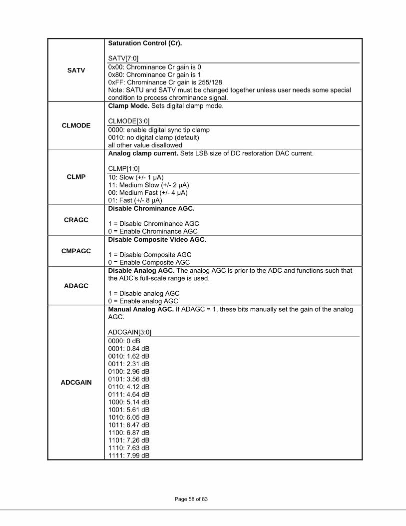
SATV
Saturation Control (Cr). SATV[7:0] 0x00: Chrominance Cr gain is 0 0x80: Chrominance Cr gain is 1 0xFF: Chrominance Cr gain is 255/128 Note: SATU and SATV must be changed together unless user needs some special condition to process chrominance signal.
CLMODE
Clamp Mode. Sets digital clamp mode. CLMODE[3:0] 0000: enable digital sync tip clamp 0010: no digital clamp (default) all other value disallowed
CLMP
Analog clamp current. Sets LSB size of DC restoration DAC current. CLMP[1:0] 10: Slow (+/- 1 μA) 11: Medium Slow (+/- 2 μA) 00: Medium Fast (+/- 4 μA) 01: Fast (+/- 8 μA)
CRAGC
Disable Chrominance AGC. 1 = Disable Chrominance AGC 0 = Enable Chrominance AGC
CMPAGC
Disable Composite Video AGC. 1 = Disable Composite AGC 0 = Enable Composite AGC
ADAGC
Disable Analog AGC. The analog AGC is prior to the ADC and functions such that the ADC’s full-scale range is used. 1 = Disable analog AGC 0 = Enable analog AGC
ADCGAIN
Manual Analog AGC. If ADAGC = 1, these bits manually set the gain of the analog AGC. ADCGAIN[3:0] 0000: 0 dB 0001: 0.84 dB 0010: 1.62 dB 0011: 2.31 dB 0100: 2.96 dB 0101: 3.56 dB 0110: 4.12 dB 0111: 4.64 dB 1000: 5.14 dB 1001: 5.61 dB 1010: 6.05 dB 1011: 6.47 dB 1100: 6.87 dB
Page 58 of 83
1101: 7.26 dB 1110: 7.63 dB 1111: 7.99 dB
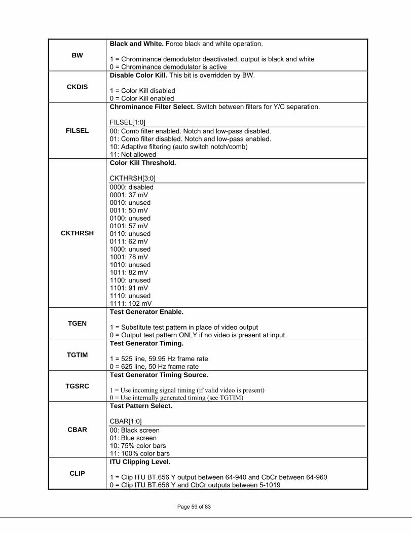
Black and White. Force black and white operation.
BW 1 = Chrominance demodulator deactivated, output is black and white 0 = Chrominance demodulator is active
CKDIS
Disable Color Kill. This bit is overridden by BW. 1 = Color Kill disabled 0 = Color Kill enabled
FILSEL
Chrominance Filter Select. Switch between filters for Y/C separation. FILSEL[1:0] 00: Comb filter enabled. Notch and low-pass disabled. 01: Comb filter disabled. Notch and low-pass enabled. 10: Adaptive filtering (auto switch notch/comb) 11: Not allowed
CKTHRSH
Color Kill Threshold. CKTHRSH[3:0] 0000: disabled 0001: 37 mV 0010: unused 0011: 50 mV 0100: unused 0101: 57 mV 0110: unused 0111: 62 mV 1000: unused 1001: 78 mV 1010: unused 1011: 82 mV 1100: unused 1101: 91 mV 1110: unused 1111: 102 mV
TGEN
Test Generator Enable. 1 = Substitute test pattern in place of video output 0 = Output test pattern ONLY if no video is present at input
TGTIM
Test Generator Timing. 1 = 525 line, 59.95 Hz frame rate 0 = 625 line, 50 Hz frame rate
TGSRC
Test Generator Timing Source. 1 = Use incoming signal timing (if valid video is present) 0 = Use internally generated timing (see TGTIM)
CBAR
Test Pattern Select. CBAR[1:0] 00: Black screen 01: Blue screen 10: 75% color bars 11: 100% color bars
CLIP
ITU Clipping Level.
Page 59 of 83
1 = Clip ITU BT.656 Y output between 64-940 and CbCr between 64-960 0 = Clip ITU BT.656 Y and CbCr outputs between 5-1019
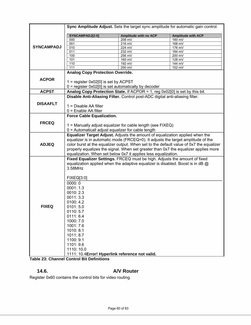
SYNCAMPADJ
Sync Amplitude Adjust. Sets the target sync amplitude for automatic gain control.
SYNCAMPADJ[2:0] Amplitude with no ACP Amplitude with ACP 000 208 mV 160 mV 001 216 mV 168 mV 010 224 mV 176 mV 011 232 mV 184 mV 100 256 mV 200 mV 101 160 mV 128 mV 110 192 mV 144 mV 111 200 mV 152 mV
ACPOR
Analog Copy Protection Override. 1 = register 0x02[0] is set by ACPST 0 = register 0x02[0] is set automatically by decoder
ACPST Analog Copy Protection State. If ACPOR = 1, reg 0x02[0] is set by this bit.
DISAAFLT
Disable Anti-Aliasing Filter. Control post-ADC digital anti-aliasing filter. 1 = Disable AA filter 0 = Enable AA filter
FRCEQ
Force Cable Equalization. 1 = Manually adjust equalizer for cable length (see FIXEQ) 0 = Automaticall adjust equalizer for cable length
ADJEQ
Equalizer Target Adjust. Adjusts the amount of equalization applied when the equalizer is in automatic mode (FRCEQ=0). It adjusts the target amplitude of the color burst at the equalizer output. When set to the default value of 0x7 the equalizer properly equalizes the signal. When set greater than 0x7 the equalizer applies more equalization. When set below 0x7 it applies less equalization.
FIXEQ
Fixed Equalizer Settings. FRCEQ must be high. Adjusts the amount of fixed equalization applied when the adaptive equalizer is disabled. Boost is in dB @ 3.58MHz FIXEQ[3:0] 0000: 0 0001: 1.3 0010: 2.3 0011: 3.3 0100: 4.2 0101: 5.0 0110: 5.7 0111: 6.4 1000: 7.0 1001: 7.6 1010: 8.1 1011: 8.7 1100: 9.1 1101: 9.6 1110: 10.0 1111: 10.4Error! Hyperlink reference not valid.
Table 23: Channel Control Bit Definitions
Page 60 of 83
14.6. A/V Router Register 0x60 contains the control bits for video routing.
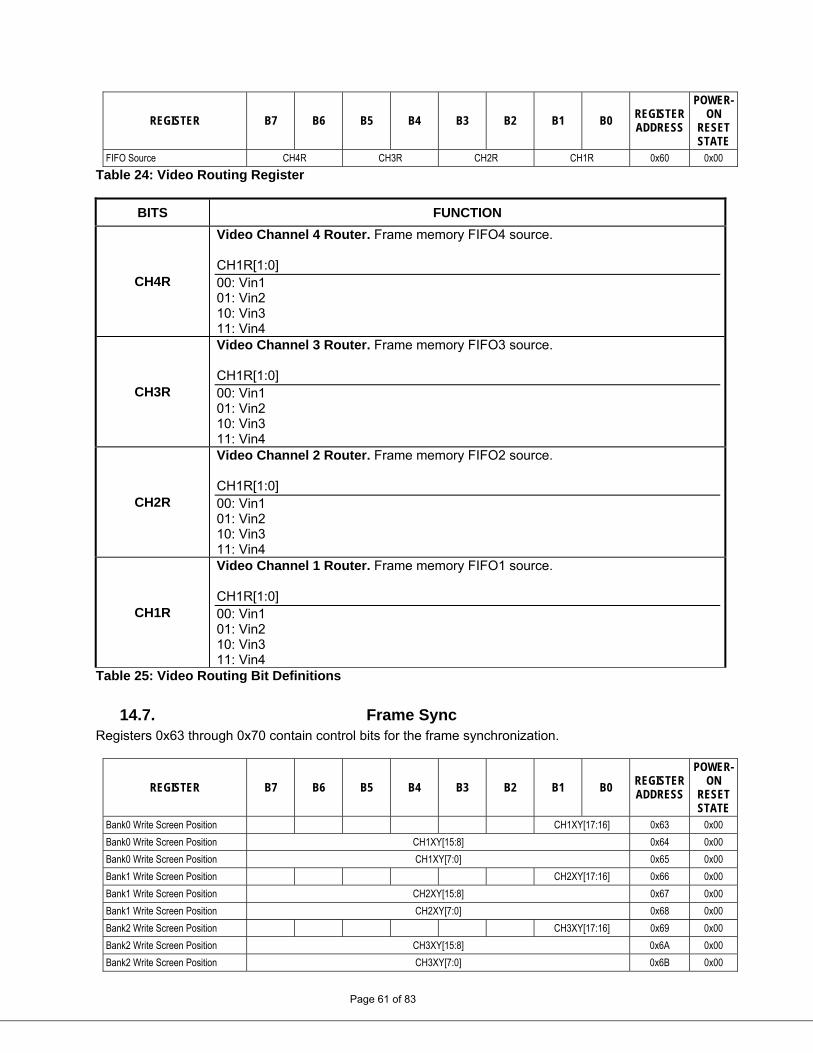
REGISTER B7 B6 B5 B4 B3 B2 B1 B0 REGISTER ADDRESS
POWER-ON
RESET STATE
FIFO Source CH4R CH3R CH2R CH1R 0x60 0x00
Table 24: Video Routing Register
BITS FUNCTION
CH4R
Video Channel 4 Router. Frame memory FIFO4 source. CH1R[1:0] 00: Vin1 01: Vin2 10: Vin3 11: Vin4
CH3R
Video Channel 3 Router. Frame memory FIFO3 source. CH1R[1:0] 00: Vin1 01: Vin2 10: Vin3 11: Vin4
CH2R
Video Channel 2 Router. Frame memory FIFO2 source. CH1R[1:0] 00: Vin1 01: Vin2 10: Vin3 11: Vin4
CH1R
Video Channel 1 Router. Frame memory FIFO1 source. CH1R[1:0] 00: Vin1 01: Vin2 10: Vin3 11: Vin4
Table 25: Video Routing Bit Definitions
14.7. Frame Sync Registers 0x63 through 0x70 contain control bits for the frame synchronization.
REGISTER B7 B6 B5 B4 B3 B2 B1 B0 REGISTER ADDRESS
POWER-ON
RESET STATE
Bank0 Write Screen Position CH1XY[17:16] 0x63 0x00
Bank0 Write Screen Position CH1XY[15:8] 0x64 0x00
Bank0 Write Screen Position CH1XY[7:0] 0x65 0x00
Bank1 Write Screen Position CH2XY[17:16] 0x66 0x00
Bank1 Write Screen Position CH2XY[15:8] 0x67 0x00
Bank1 Write Screen Position CH2XY[7:0] 0x68 0x00
Bank2 Write Screen Position CH3XY[17:16] 0x69 0x00
Bank2 Write Screen Position CH3XY[15:8] 0x6A 0x00
Bank2 Write Screen Position
Page 61 of 83
CH3XY[7:0] 0x6B 0x00
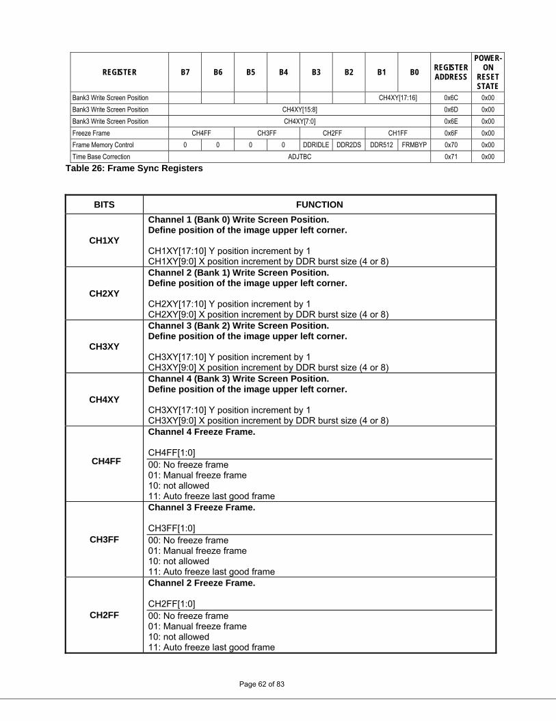
REGISTER B7 B6 B5 B4 B3 B2 B1 B0 REGISTER ADDRESS
POWER-ON
RESET STATE
Bank3 Write Screen Position CH4XY[17:16] 0x6C 0x00
Bank3 Write Screen Position CH4XY[15:8] 0x6D 0x00
Bank3 Write Screen Position CH4XY[7:0] 0x6E 0x00
Freeze Frame CH4FF CH3FF CH2FF CH1FF 0x6F 0x00
Frame Memory Control 0 0 0 0 DDRIDLE DDR2DS DDR512 FRMBYP 0x70 0x00
Time Base Correction ADJTBC 0x71 0x00
Table 26: Frame Sync Registers
BITS FUNCTION
CH1XY
Channel 1 (Bank 0) Write Screen Position. Define position of the image upper left corner. CH1XY[17:10] Y position increment by 1 CH1XY[9:0] X position increment by DDR burst size (4 or 8)
CH2XY
Channel 2 (Bank 1) Write Screen Position. Define position of the image upper left corner. CH2XY[17:10] Y position increment by 1 CH2XY[9:0] X position increment by DDR burst size (4 or 8)
CH3XY
Channel 3 (Bank 2) Write Screen Position. Define position of the image upper left corner. CH3XY[17:10] Y position increment by 1 CH3XY[9:0] X position increment by DDR burst size (4 or 8)
CH4XY
Channel 4 (Bank 3) Write Screen Position. Define position of the image upper left corner. CH3XY[17:10] Y position increment by 1 CH3XY[9:0] X position increment by DDR burst size (4 or 8)
CH4FF
Channel 4 Freeze Frame. CH4FF[1:0] 00: No freeze frame 01: Manual freeze frame 10: not allowed 11: Auto freeze last good frame
CH3FF
Channel 3 Freeze Frame. CH3FF[1:0] 00: No freeze frame 01: Manual freeze frame 10: not allowed 11: Auto freeze last good frame
CH2FF
Channel 2 Freeze Frame. CH2FF[1:0] 00: No freeze frame
Page 62 of 83
01: Manual freeze frame 10: not allowed 11: Auto freeze last good frame
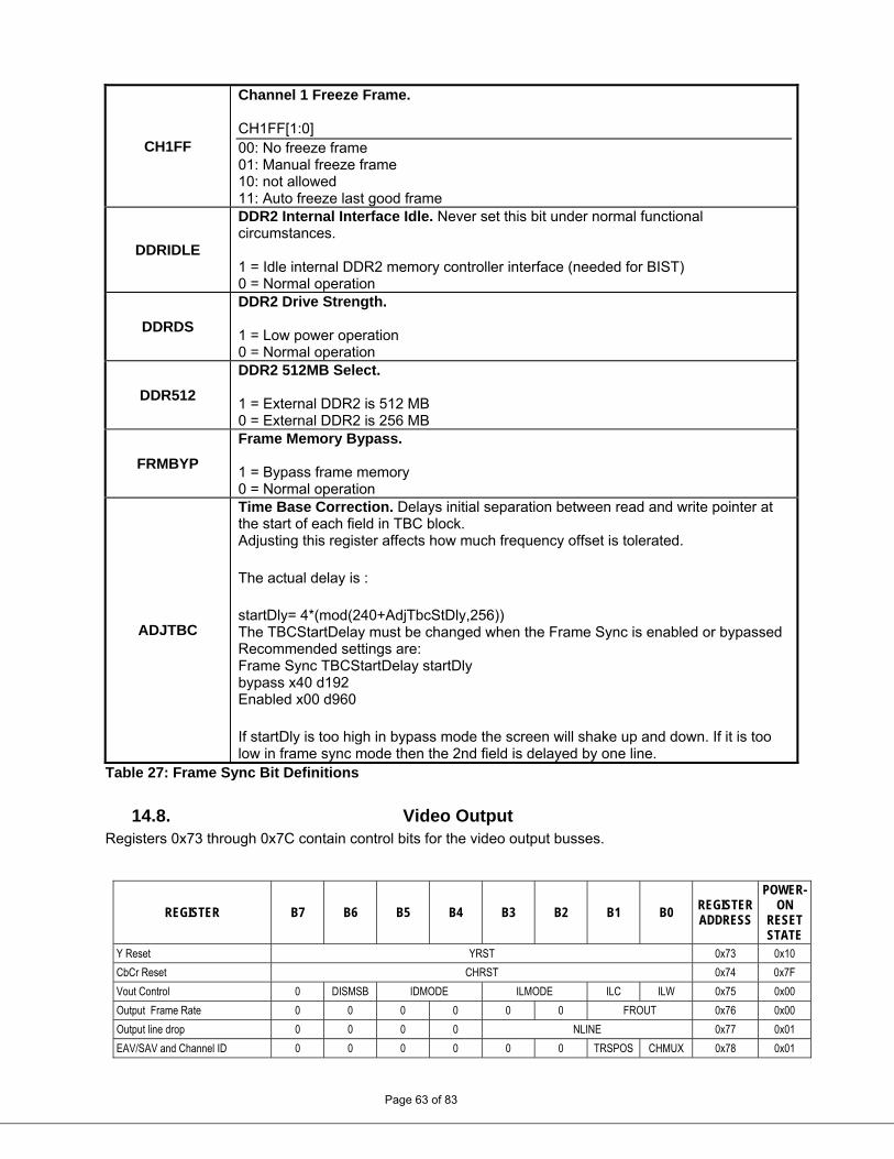
CH1FF
Channel 1 Freeze Frame. CH1FF[1:0] 00: No freeze frame 01: Manual freeze frame 10: not allowed 11: Auto freeze last good frame
DDRIDLE
DDR2 Internal Interface Idle. Never set this bit under normal functional circumstances. 1 = Idle internal DDR2 memory controller interface (needed for BIST) 0 = Normal operation
DDRDS
DDR2 Drive Strength. 1 = Low power operation 0 = Normal operation
DDR512
DDR2 512MB Select. 1 = External DDR2 is 512 MB 0 = External DDR2 is 256 MB
FRMBYP
Frame Memory Bypass. 1 = Bypass frame memory 0 = Normal operation
ADJTBC
Time Base Correction. Delays initial separation between read and write pointer at the start of each field in TBC block. Adjusting this register affects how much frequency offset is tolerated.
The actual delay is :
startDly= 4*(mod(240+AdjTbcStDly,256)) The TBCStartDelay must be changed when the Frame Sync is enabled or bypassed Recommended settings are: Frame Sync TBCStartDelay startDly bypass x40 d192 Enabled x00 d960
If startDly is too high in bypass mode the screen will shake up and down. If it is too low in frame sync mode then the 2nd field is delayed by one line.
Table 27: Frame Sync Bit Definitions
14.8. Video Output Registers 0x73 through 0x7C contain control bits for the video output busses.
REGISTER B7 B6 B5 B4 B3 B2 B0 REGISTER ADDRESS
POWER-ON
RESET STATE
B1
Y Reset YRST 0x73 0x10
CbCr Reset CHRST 0x74 0x7F
Vout Control 0 DISMSB IDMODE ILMODE ILC ILW 0x75 0x00
Output Frame Rate 0 0 0 0 0 0 FROUT 0x76 0x00
Output line drop 0 0 0 0 NLINE 0x77 0x01
EAV/SAV and Channel ID 0 0 0 0 0 0 TRSPOS
Page 63 of 83
CHMUX 0x78 0x01
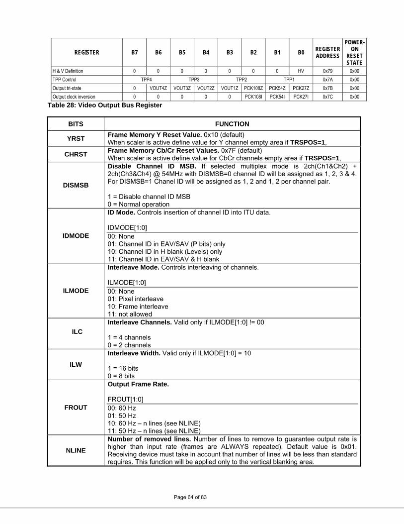
REGISTER B7 B6 B5 B4 B3 B2 B1 B0 REGISTER ADDRESS
POWER-ON
RESET STATE
H & V Definition 0 0 0 0 0 0 0 HV 0x79 0x00
TPP Control TPP4 TPP3 TPP2 TPP1 0x7A 0x00
Output tri-state 0 VOUT4Z VOUT3Z VOUT2Z VOUT1Z PCK108Z PCK54Z PCK27Z 0x7B 0x00
Output clock inversion 0 0 0 0 0 PCK108I PCK54I PCK27I 0x7C 0x00
Table 28: Video Output Bus Register
BITS FUNCTION
YRST Frame Memory Y Reset Value. 0x10 (default) When scaler is active define value for Y channel empty area if TRSPOS=1,
CHRST Frame Memory Cb/Cr Reset Values. 0x7F (default) When scaler is active define value for CbCr channels empty area if TRSPOS=1,
DISMSB
Disable Channel ID MSB. If selected multiplex mode is 2ch(Ch1&Ch2) + 2ch(Ch3&Ch4) @ 54MHz with DISMSB=0 channel ID will be assigned as 1, 2, 3 & 4. For DISMSB=1 Chanel ID will be assigned as 1, 2 and 1, 2 per channel pair. 1 = Disable channel ID MSB 0 = Normal operation
IDMODE
ID Mode. Controls insertion of channel ID into ITU data. IDMODE[1:0] 00: None 01: Channel ID in EAV/SAV (P bits) only 10: Channel ID in H blank (Levels) only 11: Channel ID in EAV/SAV & H blank
ILMODE
Interleave Mode. Controls interleaving of channels. ILMODE[1:0] 00: None 01: Pixel interleave 10: Frame interleave 11: not allowed
ILC
Interleave Channels. Valid only if ILMODE[1:0] != 00 1 = 4 channels 0 = 2 channels
ILW
Interleave Width. Valid only if ILMODE[1:0] = 10 1 = 16 bits 0 = 8 bits
FROUT
Output Frame Rate. FROUT[1:0] 00: 60 Hz 01: 50 Hz 10: 60 Hz – n lines (see NLINE) 11: 50 Hz – n lines (see NLINE)
Page 64 of 83
NLINE
Number of removed lines. Number of lines to remove to guarantee output rate is higher than input rate (frames are ALWAYS repeated). Default value is 0x01. Receiving device must take in account that number of lines will be less than standard requires. This function will be applied only to the vertical blanking area.
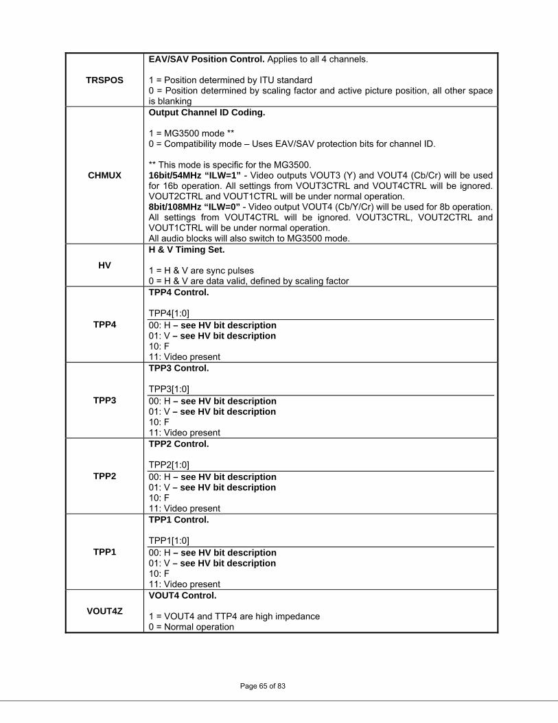
EAV/SAV Position Control. Applies to all 4 channels.
TRSPOS 1 = Position determined by ITU standard 0 = Position determined by scaling factor and active picture position, all other space is blanking
CHMUX
Output Channel ID Coding. 1 = MG3500 mode ** 0 = Compatibility mode – Uses EAV/SAV protection bits for channel ID. ** This mode is specific for the MG3500. 16bit/54MHz “ILW=1” - Video outputs VOUT3 (Y) and VOUT4 (Cb/Cr) will be used for 16b operation. All settings from VOUT3CTRL and VOUT4CTRL will be ignored. VOUT2CTRL and VOUT1CTRL will be under normal operation. 8bit/108MHz “ILW=0” - Video output VOUT4 (Cb/Y/Cr) will be used for 8b operation. All settings from VOUT4CTRL will be ignored. VOUT3CTRL, VOUT2CTRL and VOUT1CTRL will be under normal operation. All audio blocks will also switch to MG3500 mode.
HV
H & V Timing Set. 1 = H & V are sync pulses 0 = H & V are data valid, defined by scaling factor
TPP4
TPP4 Control. TPP4[1:0] 00: H – see HV bit description 01: V – see HV bit description 10: F 11: Video present
TPP3
TPP3 Control. TPP3[1:0] 00: H – see HV bit description 01: V – see HV bit description 10: F 11: Video present
TPP2
TPP2 Control. TPP2[1:0] 00: H – see HV bit description 01: V – see HV bit description 10: F 11: Video present
TPP1
TPP1 Control. TPP1[1:0] 00: H – see HV bit description 01: V – see HV bit description 10: F 11: Video present
VOUT4Z
VOUT4 Control.
Page 65 of 83
1 = VOUT4 and TTP4 are high impedance 0 = Normal operation
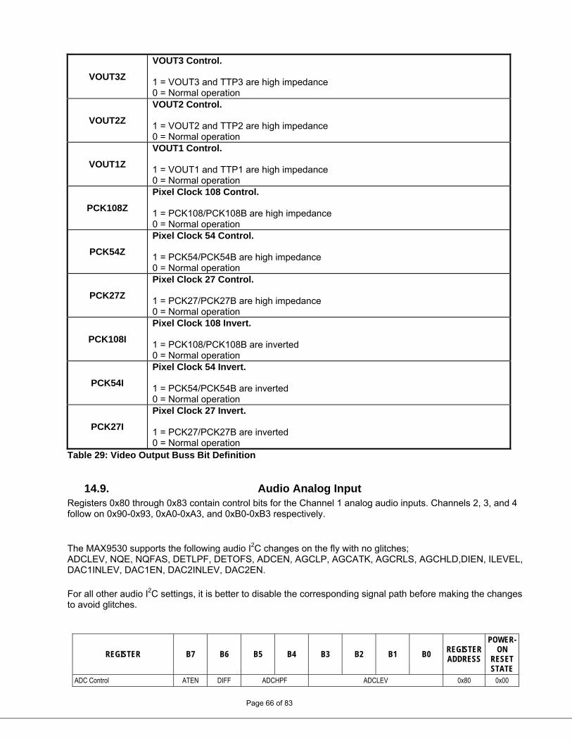
VOUT3 Control.
VOUT3Z 1 = VOUT3 and TTP3 are high impedance 0 = Normal operation
VOUT2Z
VOUT2 Control. 1 = VOUT2 and TTP2 are high impedance 0 = Normal operation
VOUT1Z
VOUT1 Control. 1 = VOUT1 and TTP1 are high impedance 0 = Normal operation
PCK108Z
Pixel Clock 108 Control. 1 = PCK108/PCK108B are high impedance 0 = Normal operation
PCK54Z
Pixel Clock 54 Control. 1 = PCK54/PCK54B are high impedance 0 = Normal operation
PCK27Z
Pixel Clock 27 Control. 1 = PCK27/PCK27B are high impedance 0 = Normal operation
PCK108I
Pixel Clock 108 Invert. 1 = PCK108/PCK108B are inverted 0 = Normal operation
PCK54I
Pixel Clock 54 Invert. 1 = PCK54/PCK54B are inverted 0 = Normal operation
PCK27I
Pixel Clock 27 Invert. 1 = PCK27/PCK27B are inverted 0 = Normal operation
Table 29: Video Output Buss Bit Definition
14.9. Audio Analog Input Registers 0x80 through 0x83 contain control bits for the Channel 1 analog audio inputs. Channels 2, 3, and 4 follow on 0x90-0x93, 0xA0-0xA3, and 0xB0-0xB3 respectively.
The MAX9530 supports the following audio I2C changes on the fly with no glitches; ADCLEV, NQE, NQFAS, DETLPF, DETOFS, ADCEN, AGCLP, AGCATK, AGCRLS, AGCHLD,DIEN, ILEVEL, DAC1INLEV, DAC1EN, DAC2INLEV, DAC2EN.
For all other audio I2C settings, it is better to disable the corresponding signal path before making the changes to avoid glitches.
REGISTER B7 B6 B5 B4 B3 B2 B1 B0 REGISTER ADDRESS
POWER-ON
RESET STATE
ADC Control ATEN DIFF ADCHPF
Page 66 of 83
ADCLEV 0x80 0x00
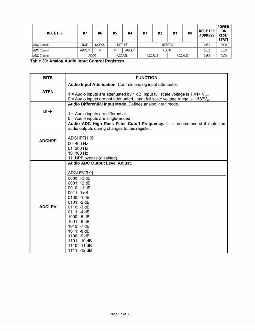
REGISTER B7 B6 B5 B4 B3 B2 B1 B0 REGISTER ADDRESS
POWER-ON
RESET STATE
ADC Control NQE NQFAS DETLPF DETOFS 0x81 0x00
ADC Control ADCEN 0 0 AGCLP AGCTH 0x82 0x00
ADC Control ADCG AGCATK AGCRLS AGCHLD 0x83 0x00
Table 30: Analog Audio Input Control Registers
BITS FUNCTION
ATEN
Audio Input Attenuation. Controls analog input attenuator. 1 = Audio inputs are attenuated by 1 dB. Input full scale voltage is 1.414 Vpp. 0 = Audio inputs are not attenuated. Input full scale voltage range is 1.587Vpp.
DIFF
Audio Differential Input Mode. Defines analog input mode. 1 = Audio inputs are differential 0 = Audio inputs are single-ended
ADCHPF
Audio ADC High Pass Filter Cutoff Frequency. It is recommended it mute the audio outputs during changes to this register. ADCHPF[1:0] 00: 400 Hz 01: 200 Hz 10: 100 Hz 11: HPF bypass (disabled)
ADCLEV
Audio ADC Output Level Adjust. ADCLEV[3:0] 0000: +3 dB 0001: +2 dB 0010: +1 dB 0011: 0 dB 0100: -1 dB 0101: -2 dB 0110: -3 dB 0111: -4 dB 1000: -5 dB 1001: -6 dB 1010: -7 dB 1011: -8 dB 1100: -9 dB
Page 67 of 83
1101: -10 dB 1110: -11 dB 1111: -12 dB
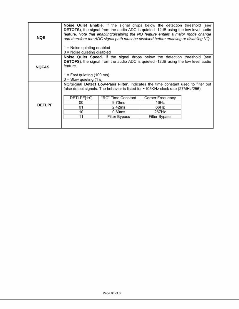
Noise Quiet Enable. If the signal drops below the detection threshold (see DETOFS), the signal from the audio ADC is quieted -12dB using the low level audio feature. Note that enabling/disabling the NQ feature entails a major mode change and therefore the ADC signal path must be disabled before enabling or disabling NQ. NQE
1 = Noise quieting enabled 0 = Noise quieting disabled
NQFAS
Noise Quiet Speed. If the signal drops below the detection threshold (see DETOFS), the signal from the audio ADC is quieted -12dB using the low level audio feature. 1 = Fast quieting (100 ms) 0 = Slow quieting (1 s)
DETLPF
NQ/Signal Detect Low-Pass Filter. Indicates the time constant used to filter out false detect signals. The behavior is listed for ~105KHz clock rate (27MHz/256)
DETLPF[1:0] “RC” Time Constant Corner Frequency 00 9.70ms 16Hz 01 2.42ms 66Hz 10 0.60ms 267Hz 11 Filter Bypass Filter Bypass
Page 68 of 83
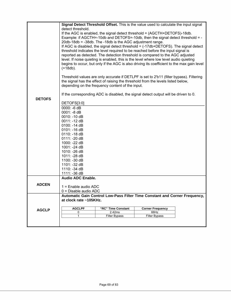
DETOFS
Signal Detect Threshold Offset. This is the value used to calculate the input signal detect threshold. If the AGC is enabled, the signal detect threshold = (AGCTH+DETOFS)-18db. Example: if AGCTH=-10db and DETOFS=-10db, then the signal detect threshold = -20db-18db = -38db. The -18db is the AGC adjustment range. If AGC is disabled, the signal detect threshold = (-17db+DETOFS). The signal detect threshold indicates the level required to be reached before the input signal is reported as detected. The detection threshold is compared to the AGC adjusted level. If noise quieting is enabled, this is the level where low level audio quieting begins to occur, but only if the AGC is also driving its coefficient to the max gain level (+18db). Threshold values are only accurate if DETLPF is set to 2'b11 (filter bypass). Filtering the signal has the effect of raising the threshold from the levels listed below, depending on the frequency content of the input. If the corresponding ADC is disabled, the signal detect output will be driven to 0. DETOFS[3:0] 0000: -6 dB 0001: -8 dB 0010: -10 dB 0011: -12 dB 0100: -14 dB 0101: -16 dB 0110: -18 dB 0111: -20 dB 1000: -22 dB 1001: -24 dB 1010: -26 dB 1011: -28 dB 1100: -30 dB 1101: -32 dB 1110: -34 dB 1111: -36 dB
ADCEN
Audio ADC Enable. 1 = Enable audio ADC 0 = Disable audio ADC
AGCLP
Automatic Gain Control Low-Pass Filter Time Constant and Corner Frequency, at clock rate ~105KHz.
AGCLPF “RC” Time Constant Corner Frequency 0 2.42ms 66Hz 1 Filter Bypass Filter Bypass
Page 69 of 83
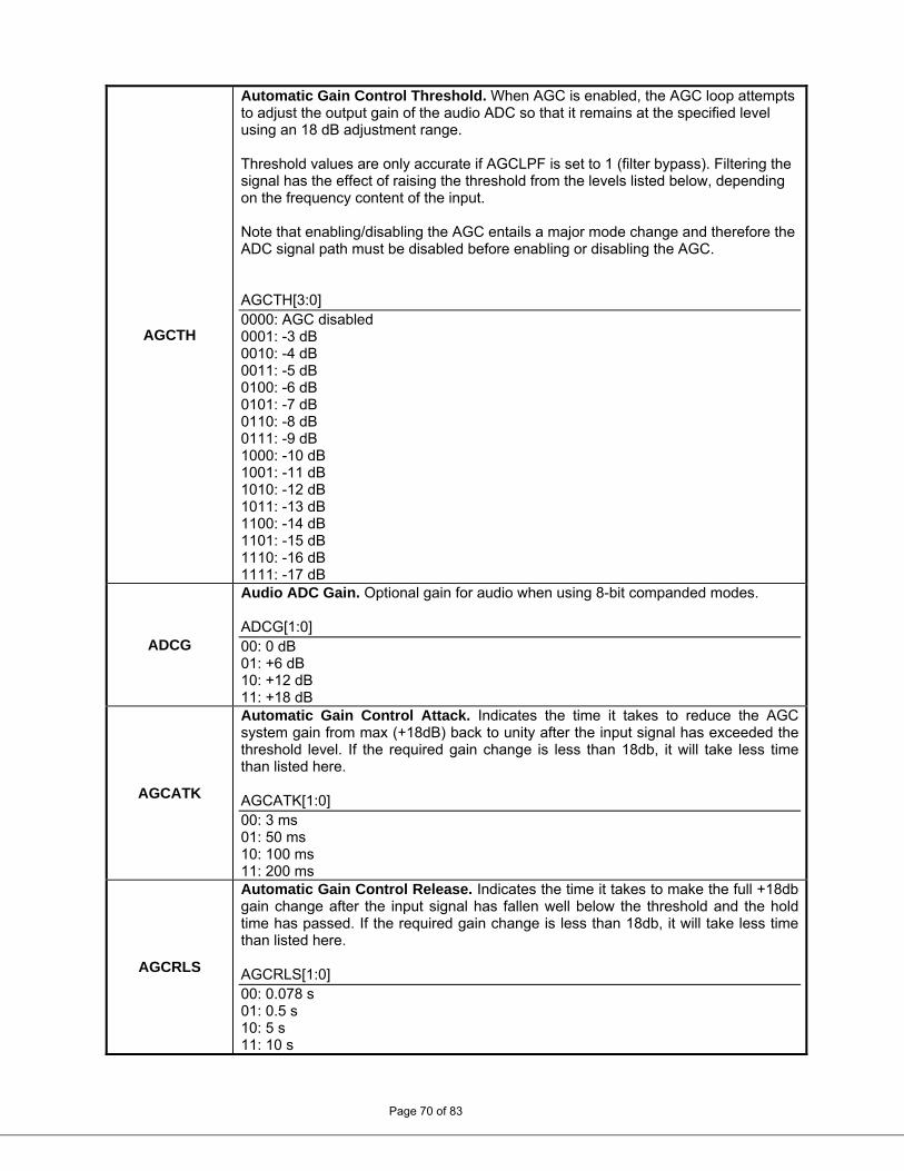
AGCTH
Automatic Gain Control Threshold. When AGC is enabled, the AGC loop attempts to adjust the output gain of the audio ADC so that it remains at the specified level using an 18 dB adjustment range. Threshold values are only accurate if AGCLPF is set to 1 (filter bypass). Filtering the signal has the effect of raising the threshold from the levels listed below, depending on the frequency content of the input. Note that enabling/disabling the AGC entails a major mode change and therefore the ADC signal path must be disabled before enabling or disabling the AGC. AGCTH[3:0] 0000: AGC disabled 0001: -3 dB 0010: -4 dB 0011: -5 dB 0100: -6 dB 0101: -7 dB 0110: -8 dB 0111: -9 dB 1000: -10 dB 1001: -11 dB 1010: -12 dB 1011: -13 dB 1100: -14 dB 1101: -15 dB 1110: -16 dB 1111: -17 dB
ADCG
Audio ADC Gain. Optional gain for audio when using 8-bit companded modes. ADCG[1:0] 00: 0 dB 01: +6 dB 10: +12 dB 11: +18 dB
AGCATK
Automatic Gain Control Attack. Indicates the time it takes to reduce the AGC system gain from max (+18dB) back to unity after the input signal has exceeded the threshold level. If the required gain change is less than 18db, it will take less time than listed here. AGCATK[1:0] 00: 3 ms 01: 50 ms 10: 100 ms 11: 200 ms
AGCRLS
Automatic Gain Control Release. Indicates the time it takes to make the full +18db gain change after the input signal has fallen well below the threshold and the hold time has passed. If the required gain change is less than 18db, it will take less time than listed here. AGCRLS[1:0] 00: 0.078 s
Page 70 of 83
01: 0.5 s 10: 5 s 11: 10 s

AGCHLD
Automatic Gain Control Hold Time. Indicates the time to hold AGC gain adjustment at its current level after an attack before releasing it. AGCHLD[1:0] 00: 50 ms 01: 100 ms 10: 200 ms 11: 400 ms
Table 31: Analog Audio Input Control Bit Definitions
14.10. Audio Digital Input Registers 0xC0 through 0xC2 contain control bits for the digital audio interfaces.
REGISTER B7 B6 B5 B4 B3 B2 B1 B0 REGISTER ADDRESS
POWER-ON
RESET STATE
Serial Input IHPF ILENA IRENA DIEN IFREQ 0xC0 0x00
Serial Input 0 0 0 ILEVEL 0xC1 0x00
Serial Input IMAS 0 ITDM IBCI IDLY IBS 0xC2 0x00
Table 32: Digital Audio Input Control Registers
BITS FUNCTION
IHPF
Audio Digital Input High Pass Filter Cutoff Frequency. IHPF[1:0] 00: 400 Hz 01: 200 Hz 10: 100 Hz 11: HPF bypass (disabled)
ILENA,IRENA
Right Channel Input Select. ILENA,IRENA 00: None selected 01: Right channel data to DAC 10: Left channel data to DAC 11: Mixed (right + left)/2 channel data to DAC
DIEN
Digital Input Enable. 1 = Enable audio digital input 0 = Disabel audio digital input
IFREQ
Audio Digital Input (LRCLKP) Frequency. IFREQ[2:0] 000: AFREQ specified 001: Not supported. 010: 16 kHz 011: 32 kHz 100: 44.1 kHz
Page 71 of 83
101: 48 kHz 110: reserved 111: reserved
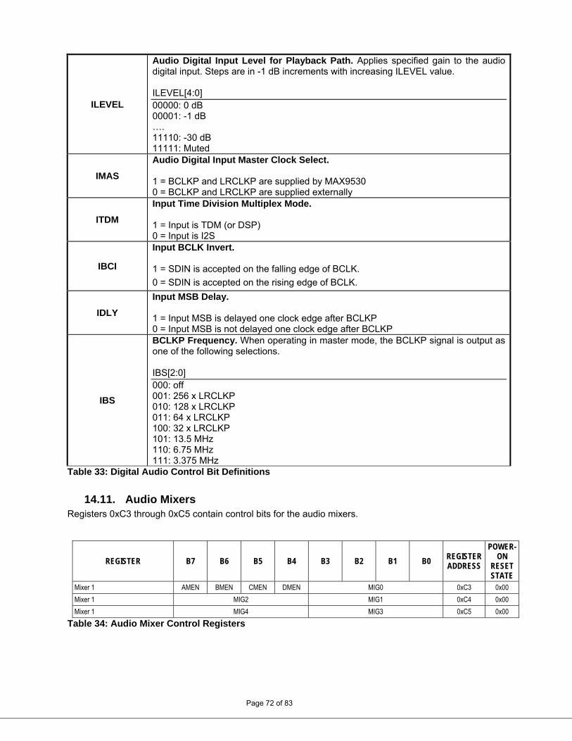
ILEVEL
Audio Digital Input Level for Playback Path. Applies specified gain to the audio digital input. Steps are in -1 dB increments with increasing ILEVEL value. ILEVEL[4:0] 00000: 0 dB 00001: -1 dB …. 11110: -30 dB 11111: Muted
IMAS
Audio Digital Input Master Clock Select. 1 = BCLKP and LRCLKP are supplied by MAX9530 0 = BCLKP and LRCLKP are supplied externally
ITDM
Input Time Division Multiplex Mode. 1 = Input is TDM (or DSP) 0 = Input is I2S
IBCI
Input BCLK Invert. 1 = SDIN is accepted on the falling edge of BCLK.
0 = SDIN is accepted on the rising edge of BCLK.
IDLY
Input MSB Delay. 1 = Input MSB is delayed one clock edge after BCLKP 0 = Input MSB is not delayed one clock edge after BCLKP
IBS
BCLKP Frequency. When operating in master mode, the BCLKP signal is output as one of the following selections. IBS[2:0] 000: off 001: 256 x LRCLKP 010: 128 x LRCLKP 011: 64 x LRCLKP 100: 32 x LRCLKP 101: 13.5 MHz 110: 6.75 MHz 111: 3.375 MHz
Table 33: Digital Audio Control Bit Definitions
14.11. Audio Mixers Registers 0xC3 through 0xC5 contain control bits for the audio mixers.
REGISTER B7 B6 B5 B4 B3 B2 B1 B0 REGISTER ADDRESS
POWER-ON
RESET STATE
Mixer 1 AMEN BMEN CMEN DMEN MIG0 0xC3 0x00
Mixer 1 MIG2 MIG1 0xC4 0x00
Mixer 1 MIG4 MIG3 0xC5 0x00
Table 34: Audio Mixer Control Registers
Page 72 of 83
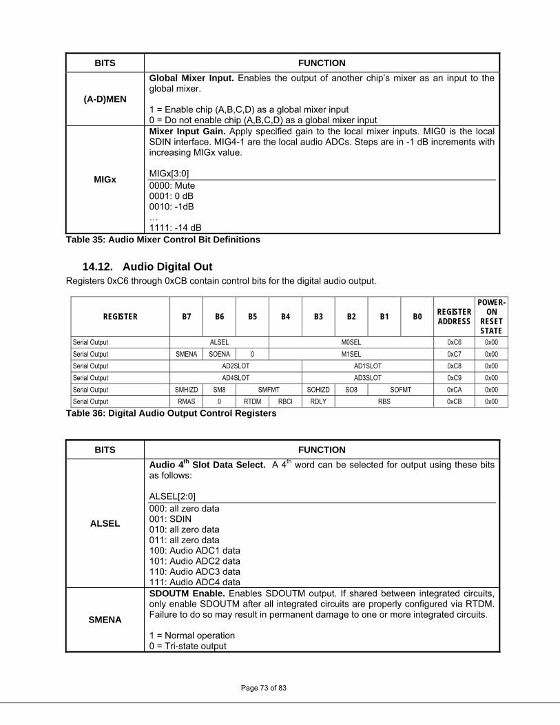
BITS FUNCTION
(A-D)MEN
Global Mixer Input. Enables the output of another chip’s mixer as an input to the global mixer. 1 = Enable chip (A,B,C,D) as a global mixer input 0 = Do not enable chip (A,B,C,D) as a global mixer input
MIGx
Mixer Input Gain. Apply specified gain to the local mixer inputs. MIG0 is the local SDIN interface. MIG4-1 are the local audio ADCs. Steps are in -1 dB increments with increasing MIGx value. MIGx[3:0] 0000: Mute 0001: 0 dB 0010: -1dB … 1111: -14 dB
Table 35: Audio Mixer Control Bit Definitions
14.12. Audio Digital Out Registers 0xC6 through 0xCB contain control bits for the digital audio output.
REGISTER B7 B6 B5 B4 B3 B2 B1 B0 REGISTER ADDRESS
POWER-ON
RESET STATE
Serial Output ALSEL M0SEL 0xC6 0x00
Serial Output SMENA SOENA 0 M1SEL 0xC7 0x00
Serial Output AD2SLOT AD1SLOT 0xC8 0x00
Serial Output AD4SLOT AD3SLOT 0xC9 0x00
Serial Output SMHIZD SM8 SMFMT SOHIZD SO8 SOFMT 0xCA 0x00
Serial Output RMAS 0 RTDM RBCI RDLY RBS 0xCB 0x00
Table 36: Digital Audio Output Control Registers
BITS FUNCTION
ALSEL
Audio 4th Slot Data Select. A 4th word can be selected for output using these bits as follows: ALSEL[2:0] 000: all zero data 001: SDIN 010: all zero data 011: all zero data 100: Audio ADC1 data 101: Audio ADC2 data 110: Audio ADC3 data 111: Audio ADC4 data
SMENA
SDOUTM Enable. Enables SDOUTM output. If shared between integrated circuits, only enable SDOUTM after all integrated circuits are properly configured via RTDM. Failure to do so may result in permanent damage to one or more integrated circuits.
Page 73 of 83
1 = Normal operation 0 = Tri-state output
SDOUT Enable. Enables SDOUT output. If shared between integrated circuits, only enable SDOUT after all integrated circuits are properly configured via RTDM. Failure to do so may result in permanent damage to one or more integrated circuits.
SOENA 1 = Normal operation 0 = Tri-state output
MxSEL
Slot 0/1 Output Select. Controls the data source for SDOUTM transfers. Slot 0 immediately follows the WCLK frame start event. Slot 1 follows Slot 0 for TDM/DSP modes. MxSEL[4:0] 0x01: Device D, Global Mixer 0x02: ADC 1 0x03: SELECT REG A 0x05: SELECT REG B 0x06: STATUS 0x07: SELECT REG C 0x09: SELECT REG D 0x0A: ADC 2 0x0B: STATUS A 0x0D: STATUS B 0x0E: Local Mixer 0x0F: Status C 0x11: Status D 0x12: ADC 3 0x13: Local Mixer A 0x15: Local Mixer B 0x16: Global Mixer 0x17: Local Mixer C 0x19: Local Mixer D 0x1A: ADC4 0x1B: Global Mixer A 0x1D: Global Mixer B
Page 74 of 83
0x1E: SDIN 0x1F: Global Mixer C other settings: all 0’s
ADxSLOT
Audio ADC Slot Selection. Controls which of the 16 SDOUT channel slots contain audio ADC data. The ADxSLOT value indicates the slot number the the corresponding audio ADC should occupy. When multiple devices are linked together using the Audio Link (AL-TDM), the SDOUT pins of all devices may be connected together and data routed to the common SDOUT bus as desired. ADxSLOT[3:0] 0000: ADCx to Slot 0 0001: ADCx to Slot 1 0010: ADCx to Slot 2 0011: ADCx to Slot 3 0100: ADCx to Slot 4 0101: ADCx to Slot 5 0110: ADCx to Slot 6 0111: ADCx to Slot 7 1000: ADCx to Slot 8 1001: ADCx to Slot 9 1010: ADCx to Slot 10 1011: ADCx to Slot 11 1100: ADCx to Slot 12 1101: ADCx to Slot 13 1110: ADCx to Slot 14 1111: ADCx to Slot 15
SMHIZD
SDOUTM Tri-State Control. 1 = SDOUTM does not tri-state between word outputs 0 = SDOUTM tri-states between word outputs
SM8
SDOUTM Data Width Selection. 1 = SDOUTM data is 8b wide 0 = SDOUTM data is 16b wide
SMFMT
SDOUTM Format Selection. SMFMT[1:0] 00: PCM Mode 01: MSB Inverted 10: A-Law 11: µ-Law
SOHIZD
SDOUT Tri-State Control. 1 = SDOUT does not tri-state between word outputs 0 = SDOUT tri-states between word outputs
SO8
SDOUT Data Width Selection. 1 = SDOUT data is 8b wide 0 = SDOUT data is 16b wide
SOFMT
SDOUT Format Selection. SOFMT[1:0] 00: PCM Mode 01: MSB Inverted 10: A-Law 11: µ-Law
RMAS
Audio Digital Output Master Clock Select.
Page 75 of 83
1 = BCLKR and LRCLKR are supplied by MAX9530 0 = BCLKR and LRCLKR are supplied externally
Output Time Division Multiplex Mode.
RTDM 1 = Output is TDM (or DSP) 0 = Output is I2S
RBCI
Output Clock Edge. 1 = SDIN and LRCLKP are clocked out on the rising edge of BCLKP 0 = SDIN and LRCLKP are clocked out on the falling edge of BCLKP
RDLY
Output MSB Delay. 1 = Output MSB is delayed one clock edge after BCLKR 0 = Output MSB is not delayed one clock edge after BCLKR
RBS
BCLKR Frequency. When operating in master mode, the BCLKR signal is output as one of the following selections. RBS[2:0] 000: off 001: 256 x LRCLKR 010: 128 x LRCLKR 011: 64 x LRCLKR 100: 32 x LRCLKR 101: 13.5 MHz 110: 6.75 MHz 111: 3.375 MHz
Table 37: Digital Audio Output Control Bit Definitions
14.13. Audio Analog Out Registers 0xD0 through 0xD5 contain control bits for analog audio output.
REGISTER B7 B6 B5 B4 B3 B2 B1 B0 REGISTER ADDRESS
POWER-ON
RESET STATE
Audio Out 1 DAC1HPF DAC1EN DAC1SEL 0xD0 0x00
Audio Out 1 DAC1INLEV 0xD1 0x00
Audio Out 1 DAC1MIXLEV 0xD2 0x00
Audio Out 2 DAC2HPF DAC2EN DAC2SEL 0xD3 0x00
Audio Out 2 DAC2INLEV 0xD4 0x00
Audio Out 2 DAC2MIXLEV 0xD5 0x00
Table 38: Analog Audio Output Control Registers
BITS FUNCTION
DACxHPF
Audio DAC High Pass Filter Cutoff Frequency. DACxHPF[1:0] 00: 400 Hz 01: 200 Hz 10: 100 Hz 11: HPF bypass (disabled)
DACxEN
Audio DAC Enabl;e.
Page 76 of 83
1 = Enable audio DACx 0 = Disable audio DACx
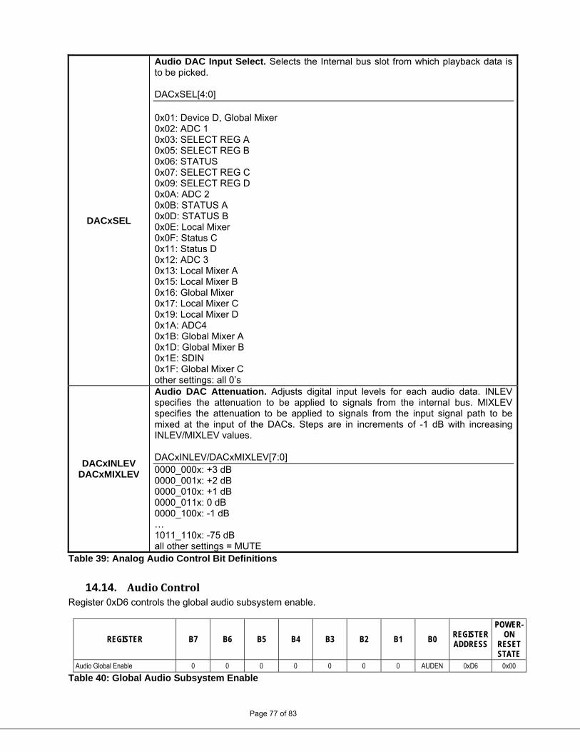
DACxSEL
Audio DAC Input Select. Selects the Internal bus slot from which playback data is to be picked. DACxSEL[4:0] 0x01: Device D, Global Mixer 0x02: ADC 1 0x03: SELECT REG A 0x05: SELECT REG B 0x06: STATUS 0x07: SELECT REG C 0x09: SELECT REG D 0x0A: ADC 2 0x0B: STATUS A 0x0D: STATUS B 0x0E: Local Mixer 0x0F: Status C 0x11: Status D 0x12: ADC 3 0x13: Local Mixer A 0x15: Local Mixer B 0x16: Global Mixer 0x17: Local Mixer C 0x19: Local Mixer D 0x1A: ADC4 0x1B: Global Mixer A 0x1D: Global Mixer B 0x1E: SDIN 0x1F: Global Mixer C other settings: all 0’s
DACxINLEV DACxMIXLEV
Audio DAC Attenuation. Adjusts digital input levels for each audio data. INLEV specifies the attenuation to be applied to signals from the internal bus. MIXLEV specifies the attenuation to be applied to signals from the input signal path to be mixed at the input of the DACs. Steps are in increments of -1 dB with increasing INLEV/MIXLEV values. DACxINLEV/DACxMIXLEV[7:0] 0000_000x: +3 dB 0000_001x: +2 dB 0000_010x: +1 dB 0000_011x: 0 dB 0000_100x: -1 dB … 1011_110x: -75 dB all other settings = MUTE
Table 39: Analog Audio Control Bit Definitions
14.14. Audio Control Register 0xD6 controls the global audio subsystem enable.
REGISTER B7 B6 B5 B4 B3 B2 B1 B0 REGISTER ADDRESS
POWER-ON
RESET STATE
Audio Global Enable 0 0 0 0 0 0 0 AUDEN 0xD6 0x00
Table 40: Global Audio Subsystem Enable
Page 77 of 83
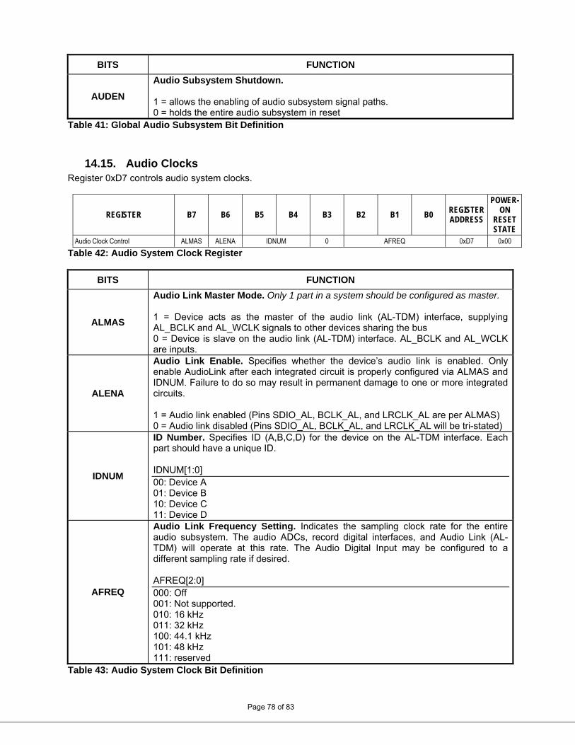
BITS FUNCTION
Audio Subsystem Shutdown. 1 = allows the enabling of audio subsystem signal paths.
AUDEN
0 = holds the entire audio subsystem in reset Table 41: Global Audio Subsystem Bit Definition
14.15. Audio Clocks Register 0xD7 controls audio system clocks.
REGISTER B7 B6 B5 B4 B3 B2 B1 B0 REGISTER ADDRESS
POWER-ON
RESET STATE
Audio Clock Control ALMAS ALENA IDNUM 0 AFREQ 0xD7 0x00
Table 42: Audio System Clock Register
BITS FUNCTION
ALMAS
Audio Link Master Mode. Only 1 part in a system should be configured as master. 1 = Device acts as the master of the audio link (AL-TDM) interface, supplying AL_BCLK and AL_WCLK signals to other devices sharing the bus 0 = Device is slave on the audio link (AL-TDM) interface. AL_BCLK and AL_WCLK are inputs.
ALENA
Audio Link Enable. Specifies whether the device’s audio link is enabled. Only enable AudioLink after each integrated circuit is properly configured via ALMAS and IDNUM. Failure to do so may result in permanent damage to one or more integrated circuits. 1 = Audio link enabled (Pins SDIO_AL, BCLK_AL, and LRCLK_AL are per ALMAS) 0 = Audio link disabled (Pins SDIO_AL, BCLK_AL, and LRCLK_AL will be tri-stated)
IDNUM
ID Number. Specifies ID (A,B,C,D) for the device on the AL-TDM interface. Each part should have a unique ID. IDNUM[1:0] 00: Device A 01: Device B 10: Device C 11: Device D
AFREQ
Audio Link Frequency Setting. Indicates the sampling clock rate for the entire audio subsystem. The audio ADCs, record digital interfaces, and Audio Link (AL-TDM) will operate at this rate. The Audio Digital Input may be configured to a different sampling rate if desired. AFREQ[2:0] 000: Off 001: Not supported. 010: 16 kHz 011: 32 kHz 100: 44.1 kHz 101: 48 kHz 111: reserved
Page 78 of 83
Table 43: Audio System Clock Bit Definition
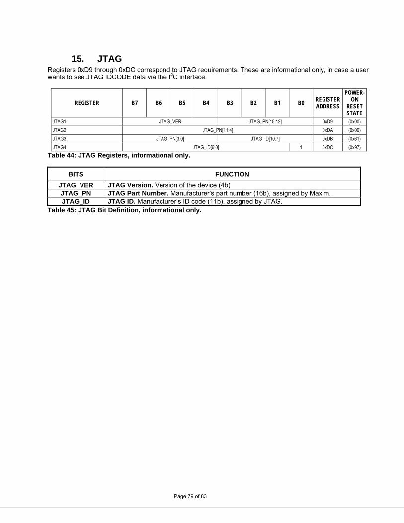
15. JTAG Registers 0xD9 through 0xDC correspond to JTAG requirements. These are informational only, in case a user wants to see JTAG IDCODE data via the I2C interface.
REGISTER B7 B6 B5 B4 B3 B2 B1 B0 REGISTER ADDRESS
POWER-ON
RESET STATE
JTAG1 JTAG_VER JTAG_PN[15:12] 0xD9 (0x00)
JTAG2 JTAG_PN[11:4] 0xDA (0x00)
JTAG3 JTAG_PN[3:0] JTAG_ID[10:7] 0xDB (0x61)
JTAG4 JTAG_ID[6:0] 1 0xDC (0x97)
Table 44: JTAG Registers, informational only.
BITS FUNCTION
JTAG Version. Version of the device (4b) JTAG_VER JTAG Part Number. Manufacturer’s part number (16b), assigned by Maxim. JTAG_PN JTAG ID. Manufacturer’s ID code (11b), assigned by JTAG. JTAG_ID
Table 45: JTAG Bit Definition, informational only.
Page 79 of 83
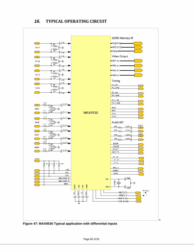
16. TYPICAL OPERATING CIRCUIT
+ Figure 47: MAX9530 Typical application with differential inputs
Page 80 of 83
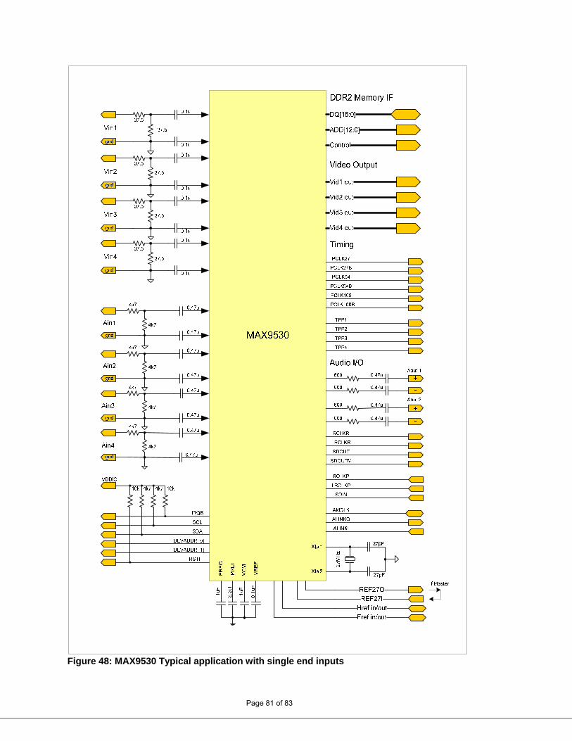
Figure 48: MAX9530 Typical application with single end inputs
Page 81 of 83
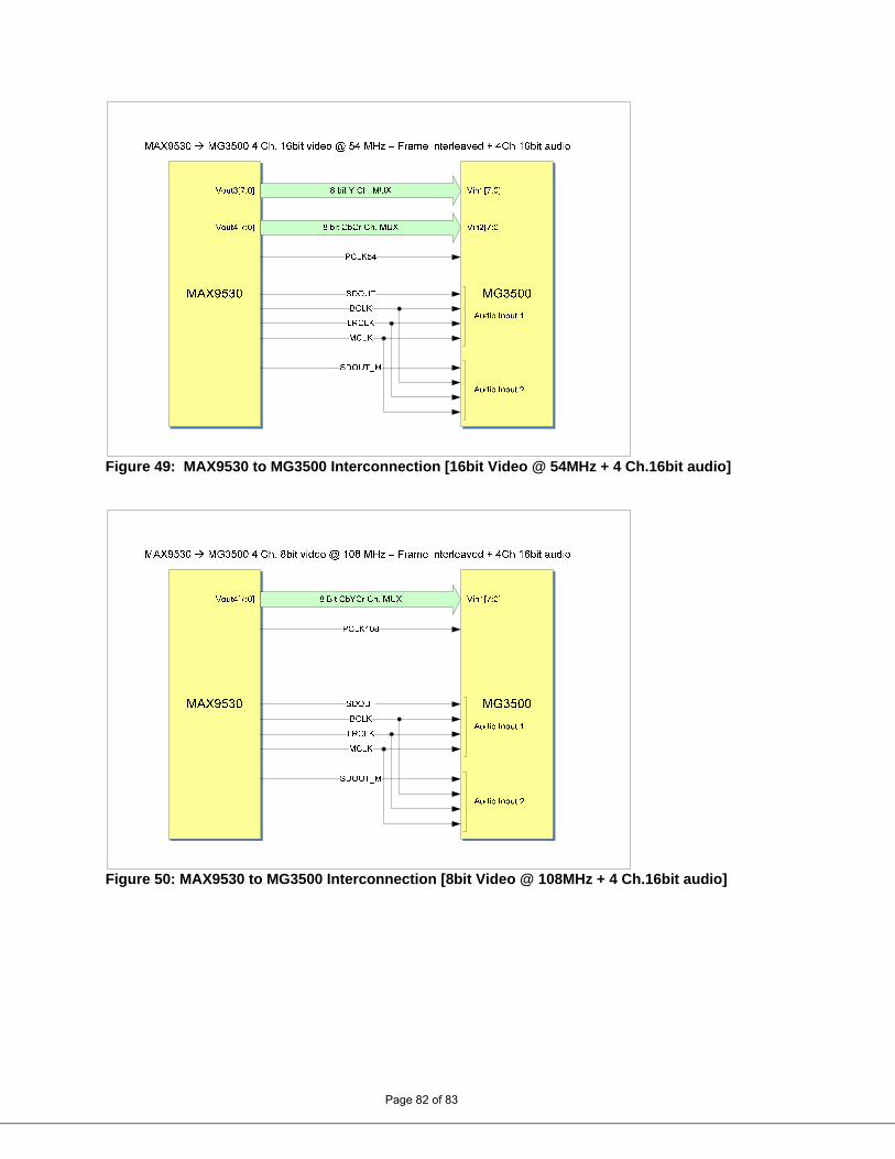
Figure 49: MAX9530 to MG3500 Interconnection [16bit Video @ 54MHz + 4 Ch.16bit audio]
Figure 50: MAX9530 to MG3500 Interconnection [8bit Video @ 108MHz + 4 Ch.16bit audio]
Page 82 of 83
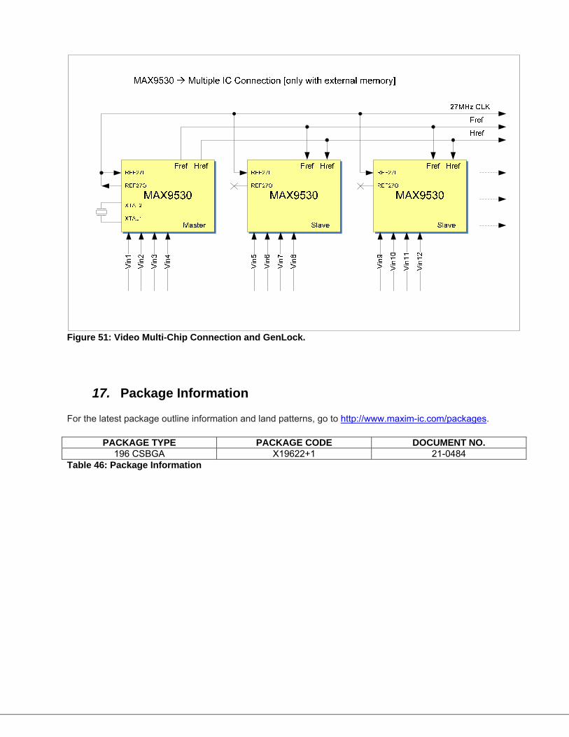
Figure 51: Video Multi-Chip Connection and GenLock.
17. Package Information For the latest package outline information and land patterns, go to http://www.maxim-ic.com/packages.
PACKAGE TYPE PACKAGE CODE DOCUMENT NO. 196 CSBGA X19622+1 21-0484
Table 46: Package Information