Q.P CODE:76197 MUMBAI UNIVERSITY - M.E. | B.Com.
27
Q.P CODE:76197 MUQuestionPapers.com MUMBAI UNIVERSITY DIGITAL LOGIC DESIGN & ANALYSIS SEMESTER 3 – CBCGS – DECEMBER 2019 Q.1 a) What are Universal gates? Why they are called so ?Explain with suitable Example . [4M] Ans : i) A universal gate is a gate which can implement any Boolean function without use any other gate type. ii) The NAND and NOR gates are universal gates. iii) AND and NOR are called universal gates because all the other gates like and,or,not,xor and xnor can be derived from it. iv) NAND GATE : NOR GATE : v) Example : OR gate using universal gate i.e NAND gate . OR gate can be implemented using three NAND gate . A B Y 0 0 1 0 1 1 1 0 1 1 1 0 A B Y 0 0 1 0 1 0 1 0 0 1 1 0
Transcript of Q.P CODE:76197 MUMBAI UNIVERSITY - M.E. | B.Com.

Q.P CODE:76197
MUQuestionPapers.com
MUMBAI UNIVERSITY
DIGITAL LOGIC DESIGN & ANALYSIS
SEMESTER 3 – CBCGS – DECEMBER 2019
Q.1 a) What are Universal gates? Why they are called so ?Explain with suitable
Example . [4M]
Ans : i) A universal gate is a gate which can implement any Boolean function without
use any other gate type.
ii) The NAND and NOR gates are universal gates.
iii) AND and NOR are called universal gates because all the other gates like
and,or,not,xor and xnor can be derived from it.
iv) NAND GATE :
NOR GATE :
v) Example : OR gate using universal gate i.e NAND gate .
OR gate can be implemented using three NAND gate .
A B Y
0 0 1 0 1 1
1 0 1
1 1 0
A B Y
0 0 1 0 1 0
1 0 0 1 1 0

Q.P CODE:76197
MUQuestionPapers.com
OR GATE USING NAND
b) Perform following substractions using 7’s complement method.
a) (𝟐𝟎)𝟓 - (𝟏𝟒)𝟓
b) (𝟐𝟎)𝟏𝟎 - (𝟏𝟓)𝟏𝟎 [4M]
Ans : a) The given numbers are of base 5 .We should convert it into octal for
Substraction process.
Using conversion table ,
(20)5 = (12)8 & (14)5 = (11)8
Here A = 12, B = 11.
Find A - B = ? using 7's complement
First find 7's complement of B = 11
Note : 7's complement of a number is obtained by subtracting all bits from 77.
7's complement of 11 is 77-11 = 66
Add it in A i.e in 12 ,
12 + 66 = 100
Here in 7s complement substraction we add carry in LSB
∴ 00 + 1 = 01
∴ (20)5 − (14)5 = (01)8

Q.P CODE:76197
MUQuestionPapers.com
b) let A = 20 and B = 15 are decimal value .
We need octal numbers for the 7s complement of any number.
∴ (20)10 = (24)8 & (15)10 = (17)8
Applying 7’s complement method on B ,
77 – 17 = 60 in octal
Add this number in A
∴ (24)8 + (60)8 = (104)8 Here carry is 1 . Add carry to LSB
∴ (20)10 - (15)10 = (5)10
c) Perform (𝟑𝟒)𝟏𝟎 − (𝟏𝟐)𝟏𝟎 in BCD using 10’s complement method . [4M]
Ans :
Here A = 34, B = 10.
Find A - B = ? using 10's complement
First find 10's complement of B = 10
Note : 10's complement of a number is 1 added to it's 9's complement number.
9's complement of 10 is
9 9
- 1 0
8 9
Now add 1 : 89 + 1 = 90

Q.P CODE:76197
MUQuestionPapers.com
Now Add this 10's complement of B to A
Here carry is 1 ; carry is ignored .,
(34)10 − (12)10 = (24)10
d) Explain lockout condition.How can it be avoided ? [4M]
Ans : i) Sometimes a counter may find itself in some unused states, this happen when
if next state of some unused state is again some unused one and if by chance the
counter happens to find itself in some unused state and never arrives at in used state
then this condition is called “Lock Out”.
ii) To avoid lock out condition the unused states are introduced in front of used states
1,4,5,6 and 7.
iii) An additional circuit is require to ensure that “lock out” does not occur. The
counter should be designed using the next state to be initial state from the unused
state.
iii)An additional circuit is require to ensure that “lock out” does not occur. The
counter should be designed using the next state to be initial state from the unused
state.
iv) To avoid lock out condition the unused states are introduced in front of used states
from the above state diagram the 1,4,5,6 and 7 is the sequence and unused states are
0,3 and 6 the states are introduced in front of us States 1,4,5 and 7 respectively.
3 4
+ 9 0
1 2 4

Q.P CODE:76197
MUQuestionPapers.com
e) If the 7 bit hamming code word received by receiver is 1011011,assuming
the even parity,state whether the received code word is correct or not.
If wrong locate the bit having error and extract corrected data. [4M]
Ans : The received data is 1101101
2𝑘 -1 >= m+k ,
23 – 1 >= 4+3 ,
7=7
Odd C1=1011
Even C2 = 1001
Odd C4 =1101
Bit error = 1+4 = 5
The correct data 1001011
Q.2 a) Reduce using Quine McClusky Method & realize the operation using
NOR gates only.
F = ∑ 𝒎(𝟎, 𝟏, 𝟐, 𝟖, 𝟏𝟎, 𝟏𝟏, 𝟏𝟒, 𝟏𝟓) [10M]
Ans : The given function contains min terms and truth table and Quine
McClusky method is given
Quine McClusky Method :

Q.P CODE:76197
MUQuestionPapers.com
Finding all prime implicants of the function.Use those prime implicants in a prime
implicant chart to find the essential prime implicants of the function, as well as other
prime implicants that are necessary to cover the function
A B C D Y
0 0 0 0 1
0 0 0 1 1
0 0 1 0 1
0 0 1 1 0
0 1 0 0 0
0 1 0 1 0 0 1 1 0 0
0 1 1 1 0
1 0 0 0 1
1 0 0 1 0
1 0 1 0 1
1 0 1 1 1
1 1 0 0 0
1 1 0 1 0
1 1 1 0 1
1 1 1 1 1
∴ y = B'D' + AC + A'B'C'

Q.P CODE:76197
MUQuestionPapers.com
Implementation :

Q.P CODE:76197
MUQuestionPapers.com
b) Explain one digit BCD Adder . [10]
Ans : I)A BCD adder adds two BCD digits and produces output as a BCD digit. A BCD or Binary
Coded Decimal digit cannot be greater than 9.
II)The two BCD digits are to be added using the rules of binary addition.
III) If sum is less than or equal to 9 and carry is 0, then no correction is needed. The sum is
correct and in true BCD form.
IV) But if sum is greater than 9 or carry =1, the result is wrong and correction must be done.
The wrong result can be corrected adding six (0110) to it.
V) For implementing a BCD adder using a binary adder circuit IC 7483, additional
combinational circuit will be required, where the Sum output S3−S0S3−S0 is checked
for invalid values from 10 to 15. The truth table and K-map for the same is as shown:

Q.P CODE:76197
MUQuestionPapers.com
VI)The Boolean expression is, Y=S3S2+S3S1Y=S3S2+S3S1
VII)The BCD adder is shown below. The output of the combinational circuit should be
1 if Cout of adder-1 is high. Therefore Y is ORed with Cout of adder 1.
VIII)The output of combinational circuit is connected to B1B2 inputs of adder-2
and B3=B1+0B3=B1+0 as they are connected to ground permanently. This
makes B3B2B1B0B3B2B1B0 = 0110 if Y' = 1.
IX) The sum outputs of adder-1 are applied to A3A2A1A0A3A2A1A0 of adder-2. The
output of combinational circuit is to be used as final output carry and the carry output
of adder-2 is to be ignored.

Q.P CODE:76197
MUQuestionPapers.com
Example :
Thus,
Cout = 1
S3S2S1S0=0000 S3S2S1S0=0000 Hence, for adder, inputs will be A3A2A1A0=0000 A3A2A1A0=0000 B3B2B1B0=0110 B3B2B1B0=0110 This will give final output as Cout S3S2S1S0=10110 S3S2S1S0=10110.
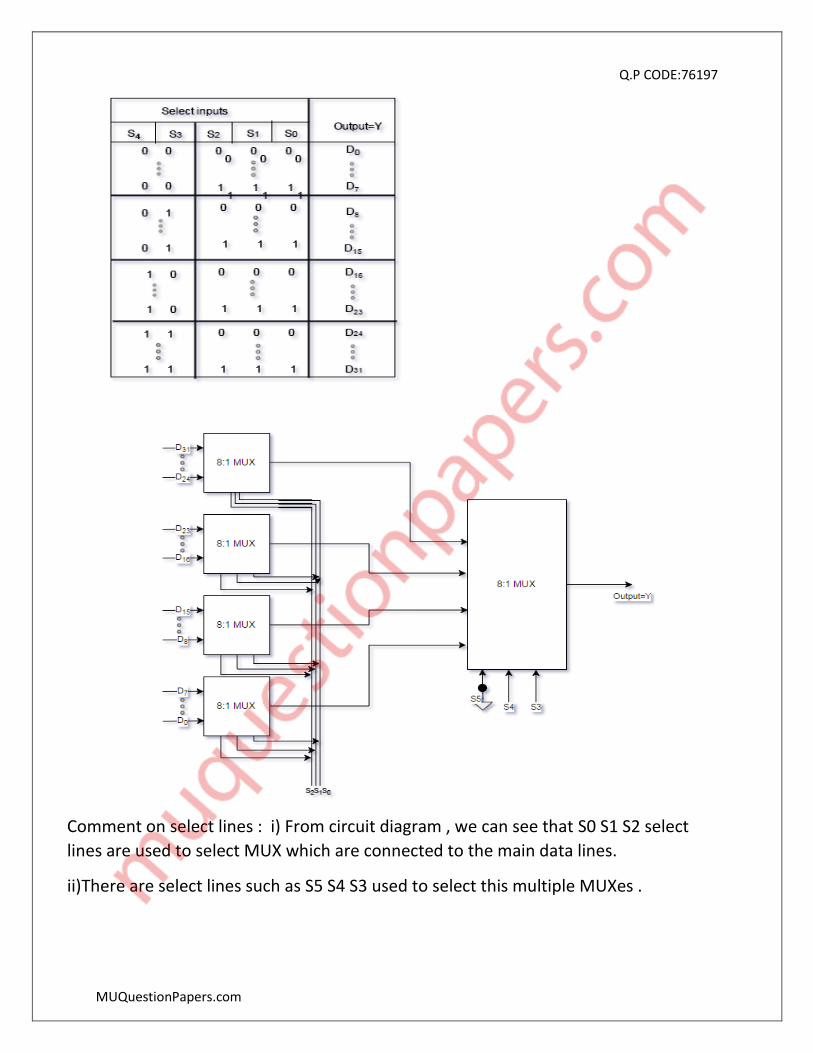
Q.3 (a) Construct 32:1 MUX using 8:1 MUX only.Also comment about select lines used [10M] Ans :
i) In electronics, a multiplexer (or mux), also known as a data selector, is a device that selects between several analog or digital input signals and forwards it to a single output line. ii) The multiplexer is a combinational logic circuit designed to switch one of several input lines to a single common output line. iii) Multiplexer are of different types .Example 2:1 MUX , 4:1 MUX , 8:1 MUX , 16:1 MUX ,32:1 MUX ,etc. iv) We can implement a MUX using different types of MUX .For example , we can Construct 32:1 MUX using 8:1 MUX only. V) Truth table and implementation of 32:1 MUX :
Q.P CODE:76197
MUQuestionPapers.com
Comment on select lines : i) From circuit diagram , we can see that S0 S1 S2 select
lines are used to select MUX which are connected to the main data lines.
ii)There are select lines such as S5 S4 S3 used to select this multiple MUXes .

Q.P CODE:76197
MUQuestionPapers.com
b) Solve the following using Kmap
F(A,B,C,D) = 𝝅𝑴(𝟑, 𝟒, 𝟓, 𝟔, 𝟕, 𝟏𝟎, 𝟏𝟏, 𝟏𝟓) [5M]
Ans : The given function contains max terms .
Truth table :
A B C D Y
0 0 0 0 1
0 0 0 1 1
0 0 1 0 1
0 0 1 1 0
0 1 0 0 0
0 1 0 1 0
0 1 1 0 0
0 1 1 1 0
1 0 0 0 1
1 0 0 1 1 1 0 1 0 0
1 0 1 1 0
1 1 0 0 1
1 1 0 1 1
1 1 1 0 1
1 1 1 1 0
KMAP :

Q.P CODE:76197
MUQuestionPapers.com
Circuit Diagram :
y = B'C' + AC' + A'B'D' + ABD'
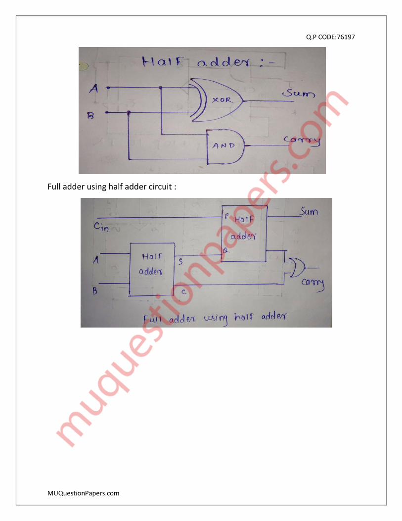
c) Design full adder using half adders and few gates. [5M]
Ans : Half Adder : The addition of 2bits is called Half adder the input variebles are
augent and addent bits and output variebles are sum&carry bits.
Full Adder : Full Adder is the adder which adds three inputs and produces two
outputs. The first two inputs are A and B and the third input is an input carry as C-
IN. The output carry is designated as C-OUT and the normal output is designated
as S which is SUM.
A B C Y(SUM) Y(CARRY)
0 0 0 0 0 0 0 1 1 0
0 1 0 1 0
0 1 1 0 1 1 0 0 1 0
1 0 1 0 1 1 1 0 0 1
1 1 1 1 1
A B Y(SUM) Y(CARRY)
0 0 0 0
0 1 1 0
1 0 1 0 1 1 0 1
HALF ADDER
Q.P CODE:76197
MUQuestionPapers.com
Full adder using half adder circuit :

Q.P CODE:76197
MUQuestionPapers.com
Q.4 a) Convert SR flip flop to JK flip flop and T flip flop. [10M]
Ans : A) SR flip flop to JK flip flop :
I) The truth tables for the flip flop conversion are given below. The present state is
represented by Qp and Qp+1 is the next state to be obtained when the J and K
inputs are applied.
II)For two inputs J and K, there will be eight possible combinations. For each
combination of J, K and Qp, the corresponding Qp+1 states are found. Qp+1
simply suggests the future values to be obtained by the JK flip flop after the value
of Qp. The table is then completed by writing the values of S and R required to get
each Qp+1 from the corresponding Qp. That is, the values of S and R that are
required to change the state of the flip flop from Qp to Qp+1 are written.
Truth Table :
J K 𝑄𝑃 𝑄𝑃+1 S R
0 0 0 0 0 X
0 0 0 1 X 0
0 0 1 0 0 X
0 0 1 0 0 1
0 1 0 1 1 0
0 1 0 1 X 0
0 1 1 1 1 0
0 1 1 0 0 1

Q.P CODE:76197
MUQuestionPapers.com
Circuit :
B) SR Flip flop to T flip flop :
Truth table of T flip flop :
T INPUT PRESENT STATE NEXT STATE
0 0 0 0 1 1
1 0 1
1 1 0
Excitation table of SR flip flop :
Present State Next state S R
0 0 0 X
0 1 1 0
1 0 0 1
1 1 x 0

Q.P CODE:76197
MUQuestionPapers.com
Combined table for conversion :
T Present Next state S R
0 0 0 0 x
0 1 1 x 0
1 0 1 1 0
1 1 0 0 1
1. Connect the S input to the output of a two-input AND gate which is driven
by the user-provided input, T, and the negation of the flip-flop's present-
state, Q̅n
2. Connect the R input to the output of a two-input AND gate which is
driven by the user-defined input, T, and the present-state of the flip-flop,
Qn
Circuit :

Q.P CODE:76197
MUQuestionPapers.com
b) Design 3-bit asynchronous up-down counter. [10M]
Ans :
i) As we know that in the up-counter each flip-flop is triggered by the normal
output of the preceding flip-flop (from output Q of first flip-flop to clock of next
flip-flop); whereas in a down-counter,
each flip-flop is triggered by the complement output of the preceding flip-flop
(from output Q^ of first flip-flop to clock of next flip-flop).
Truth table :
State Qc Qb Qa State Qc Qb Qa
0 0 0 0 7 1 1 1
1 0 0 1 6 1 1 0 2 0 1 0 5 1 0 1
3 0 1 1 4 1 0 0
4 1 0 0 3 0 1 1
5 1 0 1 2 0 1 0
6 1 1 0 1 0 0 1
7 1 1 1 0 0 0 0
i)For up down counting operation preceding flip-flop sometime it need input from
output from output Q of first flip-flop to clock of next flip-flop for up-counting and
sometimes from output Q^ of first flip-flop to clock of next flip-flop for down-
counting. So in above circuit diagram it is shown clearly.
ii) As we know a flip-flop can hold single bit so for 3 bit operation it need three
flip-flops.
iii)An inverter has been inserted in between the count-up control line and the
count-down control line to ensure that the count-up and count-down cannot be
simultaneously in the HIGH state.
iv)When the count-up/down line is held HIGH, the lower AND gates will be
disabled and their outputs will be zero.

Q.P CODE:76197
MUQuestionPapers.com
v) So they will not affect the outputs of the OR gates. At the same time the upper
AND gates will be enabled. Hence, QA will pass through the OR gate and into the
clock input of the B flip-flop.
vi)Similarly, QB will be gated into the clock input of the C flip-flop. Thus, as the
input pulses are applied, the counter will count up and follow a natural binary
counting sequence from 000 to 111.
vii)Similarly, with count-up/down line being logic 0, the upper AND gates will
become disabled and the lower AND gates are enabled, allowing Q′A and Q′B to
pass through the clock inputs of the following flip-flops.
viii)Hence, in this condition the counter will count in down mode, as the input
pulses are applied.
Designed Circuit :
Q.P CODE:76197
MUQuestionPapers.com
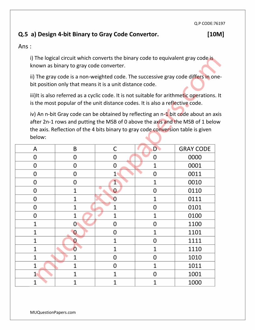
Q.5 a) Design 4-bit Binary to Gray Code Convertor. [10M]
Ans :
i) The logical circuit which converts the binary code to equivalent gray code is
known as binary to gray code converter.
ii) The gray code is a non-weighted code. The successive gray code differs in one-
bit position only that means it is a unit distance code.
iii)It is also referred as a cyclic code. It is not suitable for arithmetic operations. It
is the most popular of the unit distance codes. It is also a reflective code.
iv) An n-bit Gray code can be obtained by reflecting an n-1 bit code about an axis
after 2n-1 rows and putting the MSB of 0 above the axis and the MSB of 1 below
the axis. Reflection of the 4 bits binary to gray code conversion table is given
below:
A B C D GRAY CODE
0 0 0 0 0000
0 0 0 1 0001
0 0 1 0 0011
0 0 1 1 0010
0 1 0 0 0110
0 1 0 1 0111
0 1 1 0 0101
0 1 1 1 0100 1 0 0 0 1100
1 0 0 1 1101
1 0 1 0 1111
1 0 1 1 1110
1 1 0 0 1010
1 1 0 1 1011
1 1 1 0 1001
1 1 1 1 1000

Q.P CODE:76197
MUQuestionPapers.com
G4=∑m(8,9,10,11,12,13,14,15), G3=∑m(4,5,6,7,8,9,10,11)
G2=∑m(2,3,4,5,10,11,12,13), G1=∑m(1,2,5,6,9,10,13,14)

Q.P CODE:76197
MUQuestionPapers.com
b) What is race around condition?How it is overcome in Master slave JK
Flip flop? [5M]
Ans : Race around condition :
i) In jk flip flop there occurs a condition called race around when we put both
j and k as 1.In race around Condition till the clock is high the output varies
continuously from 0 to 1 &1 to 0.
ii) This condition is undesirable as it is of no use because the change in output
is uncontrolled.
iii) In JK flip flop as long as clock is high for the input conditions J&K equals to
the output changes or complements its output from 1–>0 and 0–>1.
iv) This is called toggling output or uncontrolled changing or racing condition.
Consider above J&K circuit diagram as long as clock is high and J&K=11
then two upper and lower AND gates are only triggered by the
complementary outputs Q and Q(bar). I.e. in any condition according to
the propagation delay one gate will be enabled and another gate is
disabled.
v) If upper gate is disabled then it sets the output and in the next lower gate
will be enabled which resets the flip flop output.
vi) If the Clock On or High time is less than the propagation delay of the flip
flop then racing can be avoided. This is done by using edge triggering
rather than level triggering.
vii) If the flip flop is made to toggle over one clock period then racing can be
avoided. This introduced the concept of Master Slave JK flip flop.

Q.P CODE:76197
MUQuestionPapers.com
c) Design 1-Bit Magnitude comparator using logic gates. [5M]
Ans : i) A comparator used to compare two bits is called a single bit comparator.
ii) It consists of two inputs each for two single bit numbers and three outputs to
generate less than, equal to and greater than between two binary numbers.
iii) A magnitude digital Comparator is a combinational circuit that compares two digital
or binary numbers in order to find out whether one binary number is equal, less than
or greater than the other binary number.
iv) We logically design a circuit for which we will have two inputs one for A and other
for B and have three output terminals, one for A > B condition, one for A = B condition
and one for A < B condition.
A A>B
B COMPARATOR A<B
A==B
Logical expression :
A>B : AB'
A<B : A'B
A=B : A'B' + AB
A B A>B A<B A==B
0 0 0 0 1
0 1 0 1 0 1 0 1 0 0
1 1 0 0 1

Q.P CODE:76197
MUQuestionPapers.com
Q. 6 Write a short note on any four [20M]
a) VHDL Modelling Styles
b) TTL and CMOS Logic Families.
c) SISO and PISO Shift Register
d) ALU
e) Twisted ring counter
Ans : A) VHDL Modelling Styles :
1] Structural modelling: in this type of modelling an entity is explained as a set of inter connected component’s.
• It shows graphical representation of modules component’s, with their inter connection.
• Structural modelling can be used to generate very high level or low level description in ckt.
2] Data flow modelling: In data flow modelling the data flow through the entity is expressed using con current signal assignment statements.
• Concurrent signal assignment statements are those in which appear outside of a process, there are event triggered.
• In signal assignment for assignment of a value to a signal symbol < = is used.

Q.P CODE:76197
MUQuestionPapers.com
3] Behavioral style of modelling:
• The behavioral level of abstraction is the level of abstraction supported in VHDL.
• Process body must be included in every behavioral description.
• The behavioral style of modelling denotes the entity behavior as a set of statements which executes sequentially.
4] Mixed style of modelling: in a single structure body, we can mix the three modelling style is within an architecture body to represent structure we can use components installation statements, to represent data flow we can use concurrent signal assignment statements and to represent behavior, we can use process statements
B) TTL and CMOS Logic Families :
i) The transistor-transistor-logic (TTL) family was developed in the use of
transistor switches for logical operations and defines the binary values as
0 V to 0.8 V = logic 0
2 V to 5 V = logic 1
ii) TTL is the largest family of digital ICs, but the CMOS family is growing rapidly.
They are inexpensive, but draw a lot of power and must be supplied with +5 volts.
Individual gates may draw 3 to 4 mA.
iii) The low power Schottky versions of TTL chips draw only 20% of the power, but
are more expensive. Part numbers for these chips have LS in the middle of them.
iv) The complementary metal oxide semiconductor family (CMOS) has equivalents
to most of the TTL chips.
v) CMOS chips are much lower in power requirements (drawing about 1 mA) and
operate with a wide range of supply voltages (typically 3 to 18 volts).
vi) The CMOS model number will have a C in the middle of it, e.g., the 74C04 is the
CMOS equivalent to the TTL 7404.

Q.P CODE:76197
MUQuestionPapers.com
vii) A high drawback is extreme sensitivity to static electricity - they must be
carefully protected from static discharges.
C) SISO and PISO Shift Register :
i) The Shift Register is another type of sequential logic circuit that can be used for
the storage or the transfer of binary data
ii) Shift Registers are used for data storage or for the movement of data and are
therefore commonly used inside calculators or computers to store data such as
two binary numbers before they are added together, or to convert the data from
either a serial to parallel or parallel to serial format.
iii) Serial-in to Serial-out (SISO) - the data is shifted serially “IN” and “OUT” of the
register, one bit at a time in either a left or right direction under clock control.
The SISO shift register is one of the simplest of the four configurations as it has
only three connections, the serial input (SI) which determines what enters the left
hand flip-flop, the serial output (SO) which is taken from the output of the right
hand flip-flop and the sequencing clock signal (Clk).
iv) Parallel-in to Serial-out (PISO) - the parallel data is loaded into the register
simultaneously and is shifted out of the register serially one bit at a time under
clock control.
The Parallel-in to Serial-out shift register acts in the opposite way to the serial-in
to parallel-out one above. The data is loaded into the register in a parallel format
in which all the data bits enter their inputs simultaneously, to the parallel input
pins PA to PD of the register. The data is then read out sequentially in the normal
shift-right mode from the register at Q representing the data present at PA to PD.
D) ALU :
i) An arithmetic logic unit (ALU) is a digital circuit used to perform arithmetic and
logic operations.

Q.P CODE:76197
MUQuestionPapers.com
ii) It represents the fundamental building block of the central processing unit
(CPU) of a computer. Modern CPUs contain very powerful and complex ALUs. In
addition to ALUs, modern CPUs contain a control unit (CU).
iii) Most of the operations of a CPU are performed by one or more ALUs, which
load data from input registers. A register is a small amount of storage available as
part of a CPU.
iv) The control unit tells the ALU what operation to perform on that data, and the
ALU stores the result in an output register. The control unit moves the data
between these registers, the ALU, and memory.
v) An ALU performs basic arithmetic and logic operations. Examples of arithmetic
operations are addition, subtraction, multiplication, and division. Examples of
logic operations are comparisons of values such as NOT, AND, and OR.
vi) All information in a computer is stored and manipulated in the form of binary
numbers, i.e. 0 and 1. Transistor switches are used to manipulate binary numbers
since there are only two possible states of a switch: open or closed.
vii) An open transistor, through which there is no current, represents a 0. A
closed transistor, through which there is a current, represents a 1.
E) Twisted Ring counter :
i) A twisted ring counter, also called switch-tail ring counter, walking ring
counter, Johnson counter, or Möbius counter, connects the complement of the
output of the last shift register to the input of the first register and circulates a
stream of ones followed by zeros around the ring.
ii)Ring counters are often used in hardware design (e.g. ASIC and FPGA design) to
create finite-state machines .
iii) A binary counter would require an adder circuit which is substantially more
complex than a ring counter and has higher propagation delay as the number of
bits increases, whereas the propagation delay of a ring counter will be nearly
constant regardless of the number of bits in the code.


![Q.P. Code : 03185 [Time : 2½ Hours] [ Total Marks:75] : 75 ...](https://static.fdocuments.in/doc/165x107/628f8e2290a5732933781805/qp-code-03185-time-2-hours-total-marks75-75-.jpg)