QoSMOS - CORDIS · 2017-04-20 · modulation schemes exhibiting well-controlled power leakage...
65
1 FP7-ICT-2009-4/248454 QoSMOS D4.4 QoSMOS Transceiver – Design and Performance Contractual Date of Delivery to the CEC: 31-Dec-2012 Actual Date of Delivery to the CEC: 31-Dec-2012 Editor(s): Vincent Berg (CEA) Author(s): Mario Schühler, Mengistu Tessema (Fraunofer IIS), Jean-Baptiste Doré, Xavier Popon, Ignacio Vergara, Dominique Noguet, Vincent Berg (CEA) Reviewer(s): David Depierre (TCF) Workpackage: WP4 Est. person months: 32.5PM Security: PU Nature: R Version: 1.0 Total number of pages: 65 Abstract: TV white space (TVWS) has been considered one of the very first portions of the spectrum where the concept of cognitive radio (CR) meets regulatory and actual deployment-driven requirement figures. Dynamic Spectrum Access in TVWS is likely to result in a heavily fragmented spectrum. This has required the development of a flexible RF transceiver. Furthermore, the requirement to meet the current adjacent channel leakage regulations has motivated the use of alternative multicarrier modulation schemes exhibiting well-controlled power leakage outside the useful bandwidth. The design and implementation of a Filter Bank Multicarrier Transceiver has been considered for the QoSMOS proof-of-concept prototypes. Implementation of the proposed approach is detailed. Keyword list: Cognitive Radio, Scenario, Transceiver architecture, Flexible design, Physical layer, Agile RF Transceiver, Multicarrier modulation, TVWS Quality Of Service and MObility driven cognitive radio Systems
Transcript of QoSMOS - CORDIS · 2017-04-20 · modulation schemes exhibiting well-controlled power leakage...

1
FP7-ICT-2009-4/248454
QoSMOS
D4.4
QoSMOS Transceiver – Design and Performance
Contractual Date of Delivery to the CEC: 31-Dec-2012
Actual Date of Delivery to the CEC: 31-Dec-2012
Editor(s): Vincent Berg (CEA)
Author(s): Mario Schühler, Mengistu Tessema (Fraunofer IIS), Jean-Baptiste Doré,
Xavier Popon, Ignacio Vergara, Dominique Noguet, Vincent Berg (CEA)
Reviewer(s): David Depierre (TCF)
Workpackage: WP4
Est. person months: 32.5PM
Security: PU
Nature: R
Version: 1.0
Total number of pages: 65
Abstract:
TV white space (TVWS) has been considered one of the very first portions of the spectrum where the
concept of cognitive radio (CR) meets regulatory and actual deployment-driven requirement figures.
Dynamic Spectrum Access in TVWS is likely to result in a heavily fragmented spectrum. This has
required the development of a flexible RF transceiver. Furthermore, the requirement to meet the
current adjacent channel leakage regulations has motivated the use of alternative multicarrier
modulation schemes exhibiting well-controlled power leakage outside the useful bandwidth. The
design and implementation of a Filter Bank Multicarrier Transceiver has been considered for the
QoSMOS proof-of-concept prototypes. Implementation of the proposed approach is detailed.
Keyword list:
Cognitive Radio, Scenario, Transceiver architecture, Flexible design, Physical layer, Agile RF
Transceiver, Multicarrier modulation, TVWS
Quality Of Service and MObility driven cognitive radio Systems
2
Abbreviations
AP Access Point
ACLR Adjacent Channel Leakage Ratio
ADC Analogue-digital converter
AGC Automatic gain control
BAW Bulk Acoustic Wave (Filter)
BB Base Bband
BCC Block Convolutional Code
CR Cognitive Radio
CW Continuous wave
DAC Digital-analogue converter
DSA Dynamic Spectrum Access
DSO Digital Switch Over
DTC Digitally tuneable capacitor/capacitance
DTT Digital Terrestrial Television
EIRP Equivalent Isotropically Radiated Power
FBMC Filter Bank Multicarrier (Modulation)
FD Fixed Device(s)
FEC Forward Error Correction
FFT Fast Fourier Transform
FIFO First-In First-Out (memory)
FM Frequency Modulated (signal)
FPGA Field Programmable Gate Array
GUI Graphical User Interface
IF Intermediate frequency
IIP3 Input intercept point of third order
IP3 Intercept point of third order

3
ISM Industrial, Scientific and Medical band
LDO Low drop-out
LDPC Low Density Parity Check (FEC)
LED Light-emitting diode
LNA Low-noise amplifier
LO Local oscillator
MAC Medium Access Control
NF Noise Figure
OIP3 Output intercept point of third order
PA Power amplifier
PLL Phase-Locked Loop
PMSE Programme Making and Special Events
PPD Personal/Portable device(s)
PRBS Pseudo Random Bit Sequence
QAM Quadradure Amplitude Modulation
QoS Quality of Service
QPSK Quadrature Phase Shift Keying
RF Radiofrequency
RMS Root Mean Square
RX Receiver
S/N Signal to noise ratio
SAW Surface acoustic wave
SFDR Spurious-Ffree Ddynamic Rrange
SPI Serial Peripheral Interface
tBPF Tuneable bandpass filter
TCXO Temperature-compensated crystal oscillator
tLPF Tuneable lowpass filter
TVWS TV white space
TX Transmitter

4
UHF Ultra High Frequency (band)
USRP Universal Software Radio Peripheral
VCO Voltage controlled oscillator
WARP Wireless Open-Access Research Platform

5
Table of contents
1 EXECUTIVE SUMMARY ........................................................................................................... 9
2 INTRODUCTION ....................................................................................................................... 10
3 A FLEXIBLE TRANSCEIVER ................................................................................................. 11
3.1 THE NEED FOR A FLEXIBLE TRANSCEIVER ............................................................................. 11 3.2 FLEXIBLE TRANSCEIVER SPECIFICATIONS ............................................................................ 14
3.2.1 Requirements imposed by regulation ............................................................................ 15 3.2.2 Derived requirements and FBMC properties ................................................................ 16 3.2.3 Specification summary for QosMOS flexible transceiver .............................................. 19
4 HARDWARE ARCHITECTURE OF QOSMOS FLEXIBLE TRANSCEIVER ................. 20
4.1 TRANSCEIVER ........................................................................................................................ 20 4.2 RF BOARD .............................................................................................................................. 20
4.2.1 Receiver ......................................................................................................................... 21 4.2.2 Transmitter .................................................................................................................... 24 4.2.3 Common components .................................................................................................... 26
4.2.3.1 RF building blocks .................................................................................................... 26 4.2.3.2 LEDs .......................................................................................................................... 27 4.2.3.3 Voltage generation .................................................................................................... 27 4.2.3.4 Reference frequency .................................................................................................. 28 4.2.3.5 Digitally Tuneable RF Filters .................................................................................... 28
4.3 ANTENNA ............................................................................................................................... 30 4.4 BASEBAND TRANSCEIVER ..................................................................................................... 34
4.4.1 Overview of QosMOS baseband transceiver implementation architecture................... 34 4.4.2 Baseband transceiver waveform structure .................................................................... 36 4.4.3 Baseband Transceiver Core Architecture ..................................................................... 36
4.4.3.1 Baseband Transmitter Core Architecture .................................................................. 36 4.4.3.2 Baseband Receiver Core Architecture ....................................................................... 38
4.5 TRANSCEIVER INTERFACES ................................................................................................... 40 4.5.1 RF Interface baseband TX and RX interface ................................................................. 40 4.5.2 Baseband Digital Interface – Dynamic and Flexible parameters ................................. 41
5 PERFORMANCE OF QOSMOS FLEXIBLE TRANSCEIVER ........................................... 45
5.1 RF TRANSCEIVER PERFORMANCE ......................................................................................... 45 5.1.1 RF RX Board Measurement........................................................................................... 45
5.1.1.1 IF Output Spectrum ................................................................................................... 45 5.1.1.2 Noise Figure .............................................................................................................. 46 5.1.1.3 Phase Noise ............................................................................................................... 48
5.1.2 Measurement TX RF board ........................................................................................... 48 5.2 BASEBAND AND RF INTEGRATED PERFORMANCE ................................................................ 49
6 CONCLUSIONS .......................................................................................................................... 54
7 REFERENCES ............................................................................................................................ 55
8 APPENDICES ............................................................................................................................. 58
8.1 FLEXIBLE INTERFACE BETWEEN ARM AND FPGA ............................................................... 58

6
List of Figures Figure 3-1: TVWS available spectrum according to [OFC09].............................................................. 12
Figure 3-2: Example of spectrum availability in London [NEK10] ...................................................... 12
Figure 3-3: General Architecture of QoSMOS Hardware platform ...................................................... 14
Figure 3-4: Example of multicarrier-based spectrum pooling ............................................................... 18
Figure 3-5: Multicarrier-based spectrum pooling, CP-OFDM versus FBMC ....................................... 18
Figure 3-6: Dynamic Range of Receiver ............................................................................................... 19
Figure 4-1: Layout of QoSMOS flexible transceiver hardware ............................................................ 20
Figure 4-2: Block diagram of the RX RF front-end .............................................................................. 21
Figure 4-3: RX RF board top and bottom ............................................................................................. 21
Figure 4-4: Signal chain calculation for -30 dBm input CW signal level ............................................. 22
Figure 4-5: Signal chain calculation for -90 dBm input CW signal level ............................................. 23
Figure 4-6: Block diagram of the RF TX front-end .............................................................................. 24
Figure 4-7: RF TX board: top layer (left-hand side) and bottom layer (right-hand side) ..................... 24
Figure 4-8: Signal chain calculation for -5 dBm CW input signal ........................................................ 25
Figure 4-9: LEDs assembled: transmitter (left-hand side) and receiver (right-hand side) .................... 27
Figure 4-10: DC Supply of the Transmitter RF-Board ......................................................................... 28
Figure 4-11: Schematic of the tBPF filter ............................................................................................. 28
Figure 4-12: Measured magnitude response of the tBPF: The diagram shows the magnitude of the
forward transmission as a function of frequency. ......................................................................... 29
Figure 4-13: Schematic of the tLPF ...................................................................................................... 29
Figure 4-14: t-LPF filter measurement result ........................................................................................ 30
Figure 4-15: Simulation model of the TVWS antenna .......................................................................... 31
Figure 4-16: Close-up of the TVWS antenna manufactured ................................................................. 31
Figure 4-17: Measured reflection and transmission characteristic of the TVWS antenna .................... 32
Figure 4-18: Simulated radiation pattern of the TVWS antenna ........................................................... 32
Figure 4-19: Implementation structure of the digital baseband top ....................................................... 34
Figure 4-20: ARM-to-FPGA driver include file ................................................................................... 35
Figure 4-21: Example of the proposed burst structure .......................................................................... 36
Figure 4-22: Structure of the Transmitter core ...................................................................................... 37
Figure 4-23: Data Framing Generation ................................................................................................. 37
Figure 4-24: Inner Transmitter .............................................................................................................. 38
Figure 4-25: Digital Front End Tx ........................................................................................................ 38
Figure 4-26: Receiver Overview ........................................................................................................... 38
Figure 4-27: Digital Front End Rx ........................................................................................................ 39

7
Figure 4-28: Receiver Synchronization ................................................................................................. 39
Figure 4-29: Inner Receiver Architecture.............................................................................................. 40
Figure 4-30: Inner Receiver architecture ............................................................................................... 40
Figure 4-31: Flexible preamble generation ........................................................................................... 44
Figure 5-1: Test board implementation hosting a RF board .................................................................. 45
Figure 5-2: IF output spectrum measurement for 730 MHz CW input signal....................................... 46
Figure 5-3: IF output spectrum sweep with frequency from 700 MHz to 760 MHz ............................. 46
Figure 5-4: Noise figure measurement result ........................................................................................ 47
Figure 5-5: Two tone measurement result (input: CW signals) ............................................................ 47
Figure 5-6: Phase noise spectrum for a 720 MHz CW input signal ...................................................... 48
Figure 5-7: RF output spectrum measurement at 720 MHz (CW IF signal) ......................................... 49

8
List of Tables Table 3-1: Place and route report (8K FFT on XC3SD3400A) ............................................................ 13
Table 3-2: FCC and OFCOM TVWS transmit parameters ................................................................... 15
Table 3-3: Waveform Specification derived from Scenarios ................................................................ 17
Table 3-4: Waveform parameter set chosen for implementation .......................................................... 17
Table 3-5: Main Flexible Transceiver Specifications ........................................................................... 19
Table 4-1: RF RX board characteristics ................................................................................................ 23
Table 4-2: Features of TX RF-Board .................................................................................................... 26
Table 4-3: Status LED Overview for each board .................................................................................. 27
Table 4-4: DTC state mapped to pass-band of the tBPF and tLPF ....................................................... 30
Table 4-5: Characteristics of the TVWS antenna .................................................................................. 33
Table 4-6: Subsampling frequency options ........................................................................................... 41
Table 4-7: Dynamic Configuration Parameters (extract) ...................................................................... 42
Table 8-1: Dynamic Configuration Parameters ..................................................................................... 58

9
1 Executive Summary
Since the start of the Digital Switch Over (DSO) in the TV broadcast bands, an increasing number of
European and world-wide regulatory bodies and authorities are investigating the unlicensed,
opportunistic use of certain parts of the spectrum. As regulatory figures have started to converge in the
TV whitespace (TVWS), the implementation of a flexible transceiver, which meets regulatory figures
and deployment driven requirements, has become an opportunity for a potential commercial
application of Cognitive Radio (CR) concepts. This deliverable investigates the relevant building
blocks of a frequency agile and flexible transceiver in the TVWS.
The constraints imposed by Dynamic Spectrum Access (DSA) in TVWS and the business scenarios
defined in WP1 have set the specifications of a flexible transceiver in the TVWS. In order to propose
broadband solutions in the TVWS alternative multicarrier modulation schemes exhibiting well-
controlled power leakage outside the useful bandwidth have been studied. Filterbank Multicarrier
(FBMC) modulation has been considered for the QoSMOS proof-of-concept prototype as a promising
solution that exhibits well-controlled power leakage outside the useful bandwidth while adapted to
heavily fragmented spectrum.
A dynamically reconfigurable RF front-end has been developed in the 470MHz to 860MHz frequency
band. The architecture of the front-end is based on frequency agile oscillators and coupled with
tuneable bandpass and lowpass filters to control image rejection. It interfaces with a baseband
transceiver build around an ARM processor and one of the latest generations of field programmable
array (FPGA).
This architecture of the baseband transceiver has been kept modular and configurable so that the built-
in microprocessor may software control the flexible baseband and radio interface. The design of a
wideband antenna constrained by size completes the transceiver.
Performance measurement particularly on the transmitter has shown that strict Adjacent Channel
Leakage Rejection ratio (ACLR) requirements imposed by regulations are possible even with a
flexible architecture. The flexible Radiofrequency (RF) front-end, the high frequency baseband
operation, and the intrinsic properties of FBMC have made the actual implementation of QoSMOS
flexible transceiver perform beyond expected simulation results.

10
2 Introduction
An increasing number of European and world-wide regulatory bodies and authorities allow
unlicensed, opportunistic use of certain parts of the spectrum, freed by the Digital Switch Over (DSO)
in the TV broadcast bands under relaxed regulatory and administrative requirements. Therefore, TV
white space (TVWS) has been considered one of the very first portions of the spectrum where the
concepts of Cognitive Radio (CR) meet regulatory and actual deployment-driven requirement figures.
In order to avoid possible harmful interference with incumbent TV broadcasting systems and wireless
microphones, these opportunistic devices need to comply with certain limitations. These include their
effective radiated power and adjacent-channel leakage requirements. Current regulations specify
relatively strict requirements which pose challenges on the implementation using conventional
modulation schemes and signal processing techniques.
As stipulated in the P1900.7 contribution [BER11], the LTE downlink waveform requires additional
filtering to meet the -55 dB ACLR requirement which in turn leads to significant complexity increase
in the implementation. Furthermore, Dynamic Spectrum Access (DSA) in TVWS is likely to result in
heavily fragmented spectrum. Filter Bank Multicarrier Modulation (FBMC) has been considered well
suited and a first implementation geared towards these applications is proposed in this document.
Section 3 recalls the specificities of TVWS and derives the requirements for a flexible transceiver in
this context. These requirements served as a basis for the development of the flexible transceiver.
Section 4 presents the architecture of the implemented FBMC flexible transceiver. RF hardware and
baseband architectures are detailed with a particular emphasis on the trade-off made for flexible
cognitive radio usage.
Section 5 gives performance results of the transceiver. Particularly, ACLR requirements are validated
in both contexts: single frequency transmission and spectrum pooling. Preliminary results of the
receiver are also given.
Finally, section 6 gives the conclusions that can be drawn from this work, the chapter also points the
way ahead to further work that should be undertaken to complement the reported findings.

11
3 A Flexible Transceiver
3.1 The need for a flexible transceiver
CR was first introduced by Mitola [Mit00] as a radio system that can adapt its parameters based upon
changes in its context environment. Whatever the origin and the nature of these changes, and the
purpose of the decision strategy, the ability to adapt to changes is essential to the concept. Therefore,
CR has capitalized on the flexible radio concept in a broad sense, or according to Mitola on the
software radio concept he introduced in [MIT95].
More recent work has focussed on opportunistic radio, where contextual environment is limited to the
knowledge of spectrum usage [ORAD3.3]. The architectural work introduced in Oracle focussed on a
multi-band transceiver, where each band was addressed individually by a specific BAW filter to
guarantee low adjacent leakage at the transmitter. Although the concept enabled some flexibility at the
modulator stage, the bands of interest were predetermined by the Bulk Acoustic Wave (BAW) filters
for which tunability is limited. Other experimental setups were limited to Industrial, Scientific and
Medical band (ISM) radiofrequency bands in order to restrict the requirements on the RF stages
[RAY05, MIS05, BIA09]. These setups enabled to test algorithms in an unlicensed environment, but
their impact on actual deployment was limited due to the competition of well-established
communication systems in these bands. Therefore these setups did not demonstrate all the potential of
cognitive radio.
In some countries, the DSO in TV bands has recently resulted in relaxed regulatory regimes, where
unlicensed spectrum use is allowed, provided that non-harmful interference to incumbent systems is
guaranteed. This move was first initiated in the USA, where the first proposed rules for the
“Unlicensed Operation in the TV Broadcast Bands” were published as early as 2004 [FCC04] and
finalized in 2009 [FCC09]. A same initiative followed in the UK [OFC09]. A similar trend is currently
taking place in other European countries [CEPT09] and in Australia [FRE11]. Consequently, the
unused TV spectrum, referred to as TVWS, has become one of the very first portions of the spectrum
where the concepts of CR meet regulatory and actual deployment-driven requirement figures. In the
meantime, standardization efforts pushed by the IEEE 802 groups [802.22, 802.11af], has given DSA
for wireless users an opportunity for practical deployment in the TVWS. The recently established
working group IEEE P1900.7 on White Space Radio has given even more momentum to this trend and
is perceived as a real opportunity for future DSA and flexible radio developments.
In [OFC09] it was made clear that opportunities for TVWS DSA exist, but that available channels
depend on location and time (Figure 3-1).

12
Figure 3-1: TVWS available spectrum according to [OFC09]
[NEK10] analysed the distribution of these channels across the TVWS spectrum (Figure 3-2). It can be
concluded from this study that an efficient exploitation of the spectrum asset depends on the ability of
the TVWS radio to exploit fragmented spectrum.
Figure 3-2: Example of spectrum availability in London [NEK10]
From these conclusions, and in order to address the scenarios considered in QoSMOS [LEH12], a set
of requirements have been derived for a CR hardware platform. In order to exercise the mobility
scenarios, the platform should be contained in size (i.e.: it should be possible to hold the demonstrator
with one hand) and battery powered. Some of the studied advanced modulations and sensing
algorithms will be evaluated in real time. The radio link and the other stages of the cognitive radio,
such as the reconfiguration of the radio should also be available on the platform. An application will
be run on top of the radio link to demonstrate Quality of Service (QoS) capability through advanced
Medium Access Control (MAC) features.
The CR hardware platform should include the following functionalities:

13
• Large bandwidth analog-to-digital and digital-to-analog conversion should interface with
an RF daughter board. • Flexible hardware, i.e. Field Programmable Gate Array (FPGA), should implement
digital-signal-processing capabilities for the implementation of the digital physical layer
multicarrier transmitter, receiver and spectrum sensing functionalities. • An embedded microprocessor should complement the FPGA to control and configure the
physical layer as well as execute the application and MAC. • Fast data interface should link the platform to provide a network connection, and interface
to a host display, and a Graphical User Interface (GUI).
In their review of cognitive radio platforms published in March 2011 [PAW11], the authors of the
review identified WARP and USRP as possible development platform. A key bottleneck in CR
implementation is underlined as appropriate frequency agile RF front-end solutions are not usually
available. Furthermore, RF front-end solutions do not couple with parts of the CR that carry out the
digital processing and thus the baseband receiver. In order to check whether off-the-shelf platform
could suit QoSMOS requirements, a benchmark of the Wireless Open-Access Research Platform
(WARP) and the Universal Software Radio Peripheral (USRP) was carried out in QoSMOS and
published in [BER12].
The WARP platform, although very flexible, has the inconvenience of being designed as a lab.
Platform and therefore not adapted to the mobile scenarios. The WARP platform, which consists of a
main FPGA board of dimension 8 x 8 inches (or approximately 203 x 203 mm), has been designed
around a Xilinx Virtex-4 but does not provide any embedded processor.
The Ettus USRP E100/E110 Embedded series seem to be better adapted as far as embedded SW and
smaller form factor are considered. Its hardware is built around a Xilinx Spartan 3A DSP FPGA and
features dual analog-to-digital converters (ADC), dual digital-to-analog converters (DAC), Embedded
OMAP module (including ARM Cortex A8 + C64 DSP) and support Angstrom Linux. In order to
evaluate whether the USRP E110 could be used to meet the requirements of the QoSMOS scenarios, a
complexity evaluation of a fundamental component used by the CR is realized. Assuming an advanced
multicarrier modulation is to be implemented on a TVWS CR physical layer, one important aspect that
should be demonstrated is the ability to provide a flexible DSA. One promising technique for DSA,
adapted to some advanced multicarrier modulations, is called spectrum pooling [WEI04]. In [BER12]
a benchmark was carried out considering spectrum pooling over 8 consecutive channels of 8MHz
each. This means that the hardware should be able to execute 8192-point (inverse) Fast Fourier
Transform (FFT or iFFT), assuming carriers are separated by 15 kHz, as is the case in the 4th
generation cellular network standards (4G LTE). This each 8-MHz channel would be implemented
with a 1024-point (i)FFT. The FPGA place and route report on the Spartan 3A FPGA of the USRP
E100/E110 platform (XC3SD3400A) as well as a static timing analysis for an 8k-FFT is given in
Table 3-1.
Table 3-1: Place and route report (8K FFT on XC3SD3400A)
Logic Utilization Ratio
Number of occupied Slices: 3,439 out of 23,872 14%
Number of DSP48As 58 out of 126 46%
Number of RAMB16BWERs 36 out of 126 28%
Static Timing Analysis
Datapath Maximum Delay Total : 5.684ns (1.783ns logic, 3.901ns route)
(31.4% logic, 68.6% route)

14
The results show that although the Spartan 3A DSP meets the requirement for one 8k FFT, significant
amount of DSP resources have been used by the operation. Considering that at least two FFT of the
evaluated size may be required (one for the transmit data path and one for receive data path), and that
timing constraints may not be met if the DSP resources are replaced by standard logic cells (Slices), it
was concluded that the Spartan 3A DSP was too resource limited for the implementation of a flexible
multi-carrier air interface application. It was therefore concluded that a specific hardware platform was
needed for the implementation of the QoSMOS radio.
3.2 Flexible Transceiver Specifications
The QoSMOS project developed therefore the hardware platform presented in Figure 3-3. The
components that are the main elements of this platform have been described in details in [D7.2] and
[D7.3].
Figure 3-3: General Architecture of QoSMOS Hardware platform
The architecture of the hardware platform proposed a software radio approach for the implementation
of the flexible transceiver. A flexible RF board is connected to the baseband through high speed
analog-to-digital converters and high speed digital-to-analog converters. Dedicated flexible RF boards
have been developed. Special care has been put in the design to meet the required TVWS
specifications. RF boards are separated into transmit and receive boards and allow flexible RF
operation of the carrier frequency and output power over the Ultra High Frequency (UHF) band from
470 MHz up to 860 MHz. Performance with regard to adjacent channel rejection ratio has been
considered as well as transmitter power in the TVWS.
Many countries have considered cognitive access to the TVWS but only the US and the UK have so
far proposed parameter figures. These first elements of specifications for the CR in the TVWS have
already been described in previous deliverables and notably in [D1.3] and [D2.3]. They are however
recalled here as they serve as a basis for the specification of the flexible transceiver developed during
the project.
JTAGXilinx
JTAGARM
TexasDM3730
XilinxXC7K325T
FlashPROM Xilinx
XCF128XBufferRS232
Quad DACAD9148
2 dual ADCAD9643
Rx I/Q
Tx I/Q
USBLink OTG
PC
PHY MACLAN9220
RFBoard
Ethernet
10/100 Mbits/sHigh-speed USB
480 Mbds

15
3.2.1 Requirements imposed by regulation
The maximum allowed transmit power of the opportunistic systems is a particularly important
parameter as it is limited to levels that ensure non-interference to DTT systems that are in the same
channel band (co-channel interference) or adjacent to the band (adjacent channel interference). The
FCC considers two types of devices. Fixed devices (FD) are allowed to operate at up to 30dBm (1W)
transmit power and with a gain antenna to achieve 36dBm (4W) EIRP. Personal/portable devices
(PPD) are allowed to operate at up to 20dBm (100mW) EIRP in non-adjacent channels. This limit is
reduced to 16dBm (40mW) EIRP when operating on a channel adjacent to a TV occupied channel. In
both cases, antenna gain is not allowed. The FCC also modifies the power requirements of PPDs
according to the way primary systems are detected. The FCC suggests that PPDs should either have
geolocation capabilities or be under the control of an FD. The FCC allows PPD that do not operate
under these conditions but rather have spectrum sensing capabilities to detect TV stations. However,
transmit power is limited to 17dBm (50mW) EIRP for these devices. Further than transmit powers, the
FCC states that out-of-band emissions should be limited to 55dB below the power level in the band
they occupy, as measured in a band of 100kHz. It should be noted that FDs are not allowed to operate
in adjacent channels, which means that the maximal interference level should be calculated
considering the 4mW condition, leading to levels similar to the one of the OFCOM (-47dBm for a
6MHz channel). OFCOM considered another approach and concluded that opportunistic system
maximal power level has to be set to 4dBm (2.5mW) EIRP in channels adjacent to DTT services.
However, in non-adjacent channels, filters have much better rejection capabilities, and 17dBm
(50mW) EIRP can be allowed in these channels. Out-of-band radiation should be kept below -46dBm.
Table 3-2: FCC and OFCOM TVWS transmit parameters
Parameter FCC OFCOM Note
Power for FD in adjacent band Not allowed Not applicable
Power for FD in non-adjacent band
with geolocation capability
30dBm Not applicable FCC: 36dBm EIRP with
a gain antenna
Power for PPD in adjacent band 16dBm 4dBm Gain antenna not allowed
Power for PPD in non-adjacent band
with geo-location capability
20dBm 17dBm Gain antenna not allowed
Power for PPD in non-adjacent band
without geo-location capability
17dBm
Out-of-band performance <55dB <-46dBm Relative to in-band power
in the case of the FCC
In-service monitoring period 60s 1s
Evacuation time 2s Not specified
For these reasons, a fare assumption is to consider that out of band adjacent channel leakage rejection
should be at least 55dB below the power emitted in band for the proposed physical layer waveform.
Another important parameter is the evacuation time imposed to leave a channel occupied by an
incumbent user. The evacuation time should be less than 2 seconds everything included. Only a
fraction of that amount of time is thus allowed for the transceiver (transmitter and receiver) to
evacuate the channel and resume communications on a different one.

16
Incumbent users are expected to be of two types:
TV channels: the signal occupies an 8MHz band within the UHF Channel and is modulated
following DVB-T or DVB-T2 standards ([DVB09] and [DVB12]).
Programme Making and Special Events (PMSE), typically wireless microphones. They use
digital modulations such as Quadrature Phase Shift Keying (QPSK) or analogue modulation
such as Frequency Modulation (FM) [ETS06]. Usually the transmitted signal is of a much
shorter bandwidth than a TV channel (i.e. around 200kHz).
3.2.2 Derived requirements and FBMC properties
A set of propagation scenarios for TVWS has been defined in WP2 and has been summarized in
[D2.3]. These propagation scenarios have themselves been derived from the business scenarios
introduced in WP1 and notably documented in [D1.3].
The set of propagation scenarios is recalled here below:
1. Indoor short range for portable devices (1-100m): this corresponds to the cognitive femtocells
and ad-hoc scenarios
2. Mobile cellular (0.1 to 2km): this corresponds to the cellular extension scenario
3. Fixed long range (1-10km): this corresponds to the dynamic backhaul and rural broadband
scenarios
For each scenario, a set of propagation parameters have been derived and are summarized in [D4.2].
These are mainly maximum RMS delay spread and maximum Doppler spread for the given scenario.
By studying multiples and submultiples of 15 kHz carrier spacing and comparing carrier spacing and
coherence bandwidth it has been possible to propose a set of parameters for which flat fading
conditions are satisfied. Then, multicarrier symbol duration and coherence time have also been
compared in order to guarantee slow fading. The results of this study have been summarized in
Table 3-3.
Multicarrier modulations are mainly characterized by the following parameters: number of carriers,
carrier spacing and symbol duration. These types of modulations impose to have the carrier spacing
smaller than the coherence bandwidth and the symbol duration smaller than the coherence time: in the
frequency domain, the channel should be constant over a subcarrier while in the time domain, the
channel should be constant during the symbol interval.

17
Table 3-3: Waveform Specification derived from Scenarios
Hypothesis
Fc 630 MHz
Channel Analysis
RMS Delay
Spread
Max Speed Max Doppler
Coherence Bandwidth
Coherence Time
Indoor Short Range 0.15 us 7 km/h 4.2 Hz 1,3 kHz 100 ms
Mobile Cellular 1.50 us 144 km/h 84.0 Hz 133 kHz 5.0 ms
Fixed Long Range 2.40 us 4 km/h 2.1 Hz 83 kHz 201 ms
FBMC Specifications
Carrier Spacing 45 kHz 30 kHz 15 kHz 7.50 kHz 3.75 kHz
Symbol Duration 22.22 us 33.33 us 66.67 us 133.33 us 266.67 us
Indoor Short Range
Coherence Bandwitdh / Carrier Spacing 30 44 89 178 356
Coherence Time / Symbol Duration 4532 3021 1511 755 378
Mobile Cellular
Coherence Bandwitdh / Carrier Spacing 3 4 9 18 36
Coherence Time / Symbol Duration 227 151 76 38 19
Fixed Wireless
Coherence Bandwitdh / Carrier Spacing 2 3 6 11 22
Coherence Time / Symbol Duration 9064 6043 3021 1511 755
The waveform parameter set proposed for implementation is given in Table 3-4 and fulfils the
different scenarios considered in QoSMOS. A carrier spacing of 15kHz offers the advantage to have a
fairly large coherence time to symbol duration ratio for all the scenarios while still providing enough
margin for coherence bandwidth.
Table 3-4: Waveform parameter set chosen for implementation
Parameter Value
Carrier Spacing 15 kHz
Symbol Duration 66 us
Number of Carriers in 8MHz 1024
Number of active Carriers in 8MHz 481
FBMC has been considered in QoSMOS, and special focus has been put on OFDM/OQAM based
FBMC. As presented in [D4.1], the waveform meets the required level of out-of-band rejection ratio
and does not require the implementation of dedicated filter mask to meet adjacent channel rejection
requirements. Moreover, as mentioned in [NOG11], another property of the waveform is of particular
interest for a flexible transceiver implementation: the ability to perform spectrum aggregation.
Opportunistic users may access to a spectrum that is already heavily fragmented. If the spectral needs
are not met in a contiguous space of spectrum some form of aggregation should be realized. An
efficient form of spectrum aggregation is the OFDM-based spectrum pooling as presented in [WEI04].
The idea is to match the bandwidth of one subband with an integer multiple of the carrier spacing.

18
Figure 3-4: Example of multicarrier-based spectrum pooling
An example of multicarrier-based spectrum pooling is given in Figure 3-4. Two key advantages have
been identified for the transceiver architecture. First, the input of the IFFT can be fed with zeros at
frequencies where incumbent users are present, while vacant sub-bands are used for transmission by
the opportunistic radio. Second, the FFT operation required at the receiver to invert the modulation
may also be used to monitor spectral activity of the other users at no extra cost. Both OFDM and
FBMC may theoretically be suited to multicarrier-based spectrum pooling. However, in the TVWS
context, the 55dB adjacent channels rejection cannot be met without a very complex and
programmable band-pass transmit filter in the CP-OFDM case, whereas FBMC would simply requires
“switching on and off” the appropriate carriers at the transmitter.
Figure 3-5: Multicarrier-based spectrum pooling, CP-OFDM versus FBMC
Figure 3-5 shows the CP-OFDM spectrum in an example of spectrum pooling where channels
[-20MHz; -12MHz] and [4MHz; 20MHz] are available for secondary transmission, and frequencies
below -20MHz and above 20MHz, as well as [-12MHz; 4MHz] are allocated to incumbent system.
The OFDM transmit filter rejects adjacent band leakage power on the spectrum below -20MHz and
above 20MHz, but not in the [-12MHz; 4MHz] band. On the other hand, the FBMC built-in filtering
feature adapts to spectrum availability even in the fragmented case.
This feature has been demonstrated in [NOG11] using simulation techniques and is a key feature the
QoSMOS flexible transceiver should perform.
f
Subbands available for
opportunistic user
f
Subbands available for
opportunistic user

19
Figure 3-6: Dynamic Range of Receiver
A last important specification parameter that should be defined for the receiver is its dynamic range.
WP2 derived a minimum level of sensitivity of -90dBm in 8MHz (see [D2.3]). If we consider a
transmitter level of 17dBm and that in very short range (less than 1m) attenuation in the air is larger
than 20dB, The overall operating dynamic range of the receive signal should be between -3dBm and
-90dBm. Figure 3-6 depicts this specification.
3.2.3 Specification summary for QoSMOS flexible transceiver
Table 3-5 summarizes the main specifications for the flexible transceiver.
Table 3-5: Main Flexible Transceiver Specifications
Parameter Value Comment
Transmit Power 17 dBm Suggested OFCOM Specification
Sensitivity -90 dBm In 8MHz bandwidth
Adjacent Channel Rejection Ratio > 55 dBc
Frequency Range 470 – 860 MHz
Frequency Agility Switching time << 1s Fast Switching Time
Ability to perform spectrum pooling
17 dBm
RMS Level
@RxAntenna
connector
(8 MHz band)
RMS EIRP
@ Antenna
-3 dBm
-90 dBm
-98 dBm Thermal noise
-114 dBmQuantization noiseBO = 16dB wrt Thermal Noise
16 dB
8 dB
20
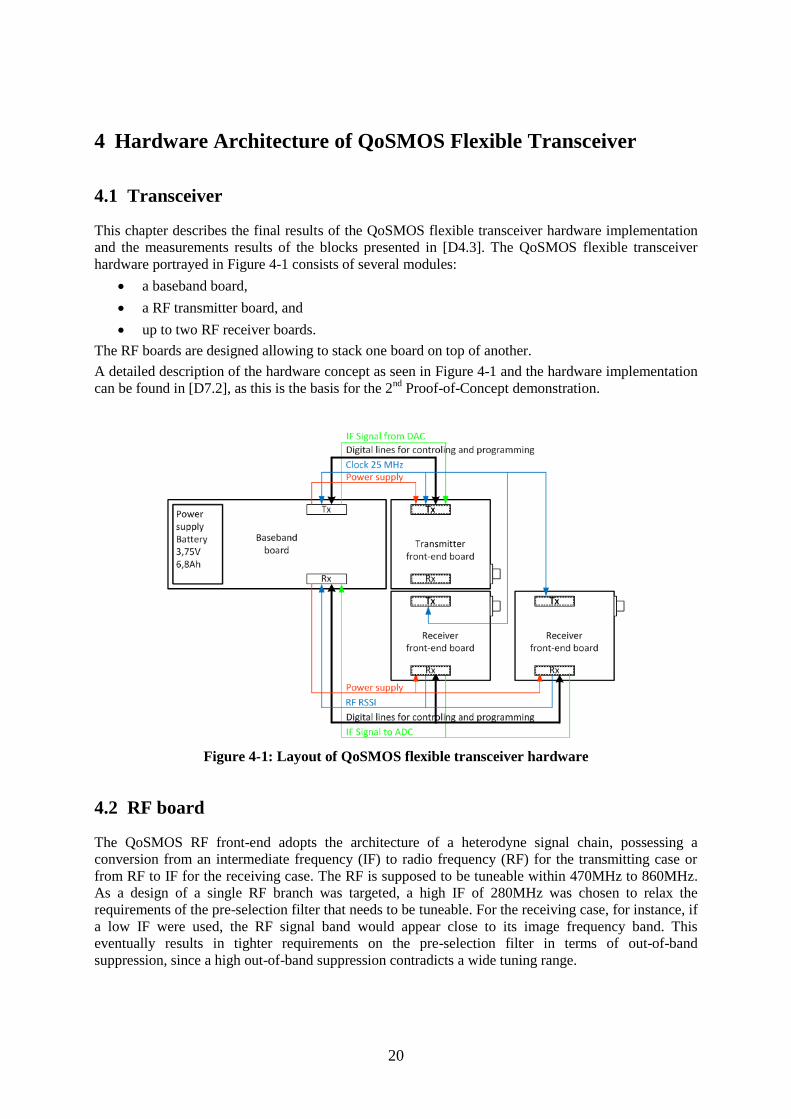
4 Hardware Architecture of QoSMOS Flexible Transceiver
4.1 Transceiver
This chapter describes the final results of the QoSMOS flexible transceiver hardware implementation
and the measurements results of the blocks presented in [D4.3]. The QoSMOS flexible transceiver
hardware portrayed in Figure 4-1 consists of several modules:
a baseband board,
a RF transmitter board, and
up to two RF receiver boards.
The RF boards are designed allowing to stack one board on top of another.
A detailed description of the hardware concept as seen in Figure 4-1 and the hardware implementation
can be found in [D7.2], as this is the basis for the 2nd
Proof-of-Concept demonstration.
Figure 4-1: Layout of QoSMOS flexible transceiver hardware
4.2 RF board
The QoSMOS RF front-end adopts the architecture of a heterodyne signal chain, possessing a
conversion from an intermediate frequency (IF) to radio frequency (RF) for the transmitting case or
from RF to IF for the receiving case. The RF is supposed to be tuneable within 470MHz to 860MHz.
As a design of a single RF branch was targeted, a high IF of 280MHz was chosen to relax the
requirements of the pre-selection filter that needs to be tuneable. For the receiving case, for instance, if
a low IF were used, the RF signal band would appear close to its image frequency band. This
eventually results in tighter requirements on the pre-selection filter in terms of out-of-band
suppression, since a high out-of-band suppression contradicts a wide tuning range.

21
4.2.1 Receiver
The RF receiver (RX) front-end architecture is illustrated in Figure 4-2 [D4.3]. The building blocks of
the RF RX board are enumerated in Section 4.2.3.1 below.
Figure 4-2: Block diagram of the RX RF front-end
Figure 4-3 shows close-ups of the RF RX board implemented in QoSMOS.
Figure 4-3: RX RF board top and bottom
The RF signal chain calculations of the RF RX front-end within the range of 710MHz to 750MHz are
depicted in Figure 4-4 assuming an input level of -30dBm and in Figure 4-5 assuming an input level of
-90dBm, respectively. The calculations show how the overall front-end characteristic is affected by its
individual components. Based on the characteristics of the individual components, the characteristics
of the whole signal chain is determined. The input parameters comprise:
Gain (G), output third order intercept point (OIP3), and noise figure (NF) of each component,
Received input power: Pout_inb ≤-30dBm (maximal level without AGC),
Received input noise power within 8MHz bandwidth: -104.9 dBm, and
Received input signal to noise ratio: S/N = 74.9dB
The output parameters derived therefrom are:
Total gain of the entire signal chain: G_all,

22
Input third order intercept point: IIP3_all_S,
Noise figure of the entire signal chain: F_all,
Spurious free dynamic range at the ouput: SFDR,
Noise power at the output within 8MHz bandwidth, and
Signal to noise ratio at the output: S/N,
which are seen at very last row (gray shaded) of the chain calculation sheet.
Figure 4-4: Signal chain calculation for -30dBm input CW signal level
wanted signal IP3 NF SFDR S/N
Pos Name
G in-
band
[dB]
OIP3
[dBm]
F
[dB]
Pout_inb
d [dBm]
G_all
[dB]
IIP3_all
_S
[dBm]
F_all
[dB]
SFDR
[dB]
Noise
Power
[dBm] S/N [dB]
input -30,0 -104,9 74,9
1 dummy 0 200 0 -30,0 0,0 200,0 0,0 203,3 -104,9 74,9
2 tLPF -1 200 1 -31,0 -1,0 197,5 1,0 200,9 -104,9 73,9
3 dummy 0 200 0 -31,0 -1,0 195,9 1,0 199,8 -104,9 73,9
4 DSA PE43702 -2 50 2 -33,0 -3,0 53,0 3,0 103,3 -104,9 71,9
5 LNA SPF-5122ZDS 20 33 1 -13,0 17,0 16,0 4,0 77,9 -83,9 70,9
6 tBPF -7 30 7 -20,0 10,0 14,5 4,1 76,9 -90,8 70,8
7 LNA SPF-5122ZDS 20 33 1 0,0 30,0 2,7 4,2 69,0 -70,7 70,7
8 DSA PE43702 -5 50 5 -5,0 25,0 2,7 4,2 68,9 -75,7 70,7
9 dummy 0 200 0 -5,0 25,0 2,7 4,2 68,9 -75,7 70,7
10 MIXER/VCO RFFC2072 -7 21 13 -12,0 18,0 -0,2 4,3 67,0 -82,6 70,6
11 dummy 0 200 0 -12,0 18,0 -0,2 4,3 67,0 -82,6 70,6
12 Low pass filter -1 200 1 -13,0 17,0 -0,2 4,3 67,0 -83,6 70,6
13 dummy 0 200 0 -13,0 17,0 -0,2 4,3 67,0 -83,6 70,6
14 IF Amp. PGA-102+ 16 30 2,5 3,0 33,0 -4,8 4,3 63,8 -67,6 70,6
15 dummy 0 200 0 3,0 33,0 -4,8 4,3 63,8 -67,6 70,6
16 SAW 280 MHz Vectron -12,3 30 12,3 -9,3 20,7 -5,0 4,3 63,7 -79,9 70,6
17 Power Splitter -3,5 200 3,5 -12,8 17,2 -5,0 4,3 63,7 -83,4 70,6
18 IF Amp. PGA-102+ 16 30 2,5 3,2 33,2 -7,2 4,4 62,2 -67,3 70,5
19 dummy 0 200 0 3,2 33,2 -7,2 4,4 62,2 -67,3 70,5
20 SAW 280 MHz Vectron -12,3 30 12,3 -9,1 20,9 -7,3 4,4 62,2 -79,6 70,5
21 dummy 0 200 0 -9,1 20,9 -7,3 4,4 62,2 -79,6 70,5
22 IF Amp. PGA-102+ 16 30 2,5 6,9 36,9 -10,1 4,4 60,3 -63,6 70,5
23 dummy 0 200 0 6,9 36,9 -10,1 4,4 60,3 -63,6 70,5
24 Low pass filter -1 200 1 5,9 35,9 -10,1 4,4 60,3 -64,6 70,5
25 dummy 0 200 0 5,9 35,9 -10,1 4,4 60,3 -64,6 70,5
26 Transformator -0,8 200 0,8 5,1 35,1 -10,1 4,4 60,3 -65,4 70,5
27 dummy 0 200 0 5,1 35,1 -10,1 4,4 60,3 -65,4 70,5
all 35,1 5,1 35,1 -10,1 4,4 60,3 -65,4 70,5
QoSMOS RX RF-Board at Temp. 25°C 730MHz

23
Figure 4-5: Signal chain calculation for -90 dBm input CW signal level
As seen in Figure 4-4 and Figure 4-5, the dynamic range without using an automatic gain control
(AGC) amounts to 60dBm, covering the range from -90dBm to -30dBm input power. The noise figure
of the whole chain is 4.4dB, the gain 35.1dB, with an S/N of 10.5dB at least.
Table 4-1 summarises the characteristics of the RF RX board.
Table 4-1: RF RX board characteristics
Parameter specification Condition
Electrical
RF Frequency range 470 MHz to 860 MHz
INPUT/OUTPUT Return loss -10 dB 50 Ohm
Input IP3 -10 dBm 2 tone
SFDR 75 dB 1 tone
System Bandwidth 40 MHz
IF centre frequency 280 MHz
Gain ca. 35 dB Without AGC
AGC Adjustment range 31 dB In 0.25 dB steps
Noise Figure < 4 dB Max. Gain
Dynamic range -87 dB
Sensitivity -90 dBm 10 dB SNR
Image rejection 75 dB
Oscillator
LO High side For whole frequency band
LO frequency 750 MHz to 1140 MHz
Phase noise -109 dBc/Hz@100kHz
Mechanical
wanted signal IP3 NF SFDR S/N
Pos Name
G in-
band
[dB]
OIP3
[dBm]
F
[dB]
Pout_inb
d [dBm]
G_all
[dB]
IIP3_all
_S
[dBm]
F_all
[dB]
SFDR
[dB]
Noise
Power
[dBm] S/N [dB]
input -90,0 -104,9 14,9
1 dummy 0 200 0 -90,0 0,0 200,0 0,0 203,3 -104,9 14,9
2 tLPF -1 200 1 -91,0 -1,0 197,5 1,0 200,9 -104,9 13,9
3 dummy 0 200 0 -91,0 -1,0 195,9 1,0 199,8 -104,9 13,9
4 DSA PE43702 -2 50 2 -93,0 -3,0 53,0 3,0 103,3 -104,9 11,9
5 LNA SPF-5122ZDS 20 33 1 -73,0 17,0 16,0 4,0 77,9 -83,9 10,9
6 tBPF -7 30 7 -80,0 10,0 14,5 4,1 76,9 -90,8 10,8
7 LNA SPF-5122ZDS 20 33 1 -60,0 30,0 2,7 4,2 69,0 -70,7 10,7
8 DSA PE43702 -5 50 5 -65,0 25,0 2,7 4,2 68,9 -75,7 10,7
9 dummy 0 200 0 -65,0 25,0 2,7 4,2 68,9 -75,7 10,7
10 MIXER/VCO RFFC2072 -7 21 13 -72,0 18,0 -0,2 4,3 67,0 -82,6 10,6
11 dummy 0 200 0 -72,0 18,0 -0,2 4,3 67,0 -82,6 10,6
12 Low pass filter -1 200 1 -73,0 17,0 -0,2 4,3 67,0 -83,6 10,6
13 dummy 0 200 0 -73,0 17,0 -0,2 4,3 67,0 -83,6 10,6
14 IF Amp. PGA-102+ 16 30 2,5 -57,0 33,0 -4,8 4,3 63,8 -67,6 10,6
15 dummy 0 200 0 -57,0 33,0 -4,8 4,3 63,8 -67,6 10,6
16 SAW 280 MHz Vectron -12,3 30 12,3 -69,3 20,7 -5,0 4,3 63,7 -79,9 10,6
17 Power Splitter -3,5 200 3,5 -72,8 17,2 -5,0 4,3 63,7 -83,4 10,6
18 IF Amp. PGA-102+ 16 30 2,5 -56,8 33,2 -7,2 4,4 62,2 -67,3 10,5
19 dummy 0 200 0 -56,8 33,2 -7,2 4,4 62,2 -67,3 10,5
20 SAW 280 MHz Vectron -12,3 30 12,3 -69,1 20,9 -7,3 4,4 62,2 -79,6 10,5
21 dummy 0 200 0 -69,1 20,9 -7,3 4,4 62,2 -79,6 10,5
22 IF Amp. PGA-102+ 16 30 2,5 -53,1 36,9 -10,1 4,4 60,3 -63,6 10,5
23 dummy 0 200 0 -53,1 36,9 -10,1 4,4 60,3 -63,6 10,5
24 Low pass filter -1 200 1 -54,1 35,9 -10,1 4,4 60,3 -64,6 10,5
25 dummy 0 200 0 -54,1 35,9 -10,1 4,4 60,3 -64,6 10,5
26 Transformator -0,8 200 0,8 -54,9 35,1 -10,1 4,4 60,3 -65,4 10,5
27 dummy 0 200 0 -54,9 35,1 -10,1 4,4 60,3 -65,4 10,5
all 35,1 -54,9 35,1 -10,1 4,4 60,3 -65,4 10,5
QoSMOS RX RF-Board at Temp. 25°C 730MHz

24
Physical dimensions 68 mm x 77 mm
Interface
RF Input SMA Female
Baseband-Board QTE/QSE connector SAMTEC
IF IN, Power supply, control
Operating Conditions
Temperature -40˚C to +85˚C
Power supply 3.7 V Single Battery via SAMTEC connector
Current consumption ca. 470 mA
Reference Frequency
Reference frequency on Board TCXO 25 MHz External via SAMTEC connector
Reference input level 800 mV p-p
4.2.2 Transmitter
The RF Transmitter (TX) front-end architecture is illustrated in Figure 4-6 [D4.3]. The building blocks
of the RF TX board are mostly adopted from the RX design, except for the LNA, which was replaced
by a power amplifier (PA). Section 4.2.3 gives an overview of the RF building blocks.
Figure 4-6: Block diagram of the RF TX front-end
Figure 4-7 shows close-ups of the RF TX board implemented.
Figure 4-7: RF TX board: top layer (left-hand side) and bottom layer (right-hand side)

25
The signal chain calculations of the RF TX front-end within the range of 710MHz to 750MHz are
depicted in Figure 4-8, Figure 4-4 assuming an input level of -5dBm. As for the receiver, the
characteristics of the individual components are given first, which comprise:
Gain (G), output third order intercept point (OIP3), and noise figure (NF) of each component,
and
Input power provided by DAC: Pout_inb ≤-5dBm (maximal level without AGC).
Then, the output characteristics are calculated including:
G_all, IIP3_all_S, F_all, SFDR
Total gain of the entire signal chain: G_all,
Input third order intercept point: IIP3_all_S, and
Spurious free dynamic range at the ouput: SFDR.
The remaining output parameters are of minor importance to the transmitting case. As seen in Figure
4-8, the output power of the transmitter amounts to 17.6dBm at most, corresponding with an SFDR of
59.1dB.
Figure 4-8: Signal chain calculation for -5 dBm CW input signal
Table 4-2 summarises the characteristics RF TX board.
wanted signal IP3 NF SFDR
Pos Name
G in-
band
[dB]
OIP3
[dBm]
F
[dB]
Pout_inb
d [dBm]
G_all
[dB]
IIP3_all
_S
[dBm]
F_all
[dB]
SFDR
[dB]
input -5,0
1 dummy 0 200 0 -5,0 0,0 200,0 0,0 203,3
2 Transformator -0,8 200 0,8 -5,8 -0,8 197,4 0,8 201,0
3 dummy 0 200 0 -5,8 -0,8 195,7 0,8 199,9
4 SAW 280 MHz Vectron -12,3 30 12,3 -18,1 -13,1 43,1 13,1 89,9
5 dummy 0 200 0 -18,1 -13,1 43,1 13,1 89,9
6 IF Amp. PGA-102+ 16 30 2,5 -2,1 2,9 27,0 15,6 77,5
7 dummy 0 200 0 -2,1 2,9 27,0 15,6 77,5
8 SAW 280 MHz Vectron -12,3 30 12,3 -14,4 -9,4 26,7 16,5 76,8
9 dummy 0 200 0 -14,4 -9,4 26,7 16,5 76,8
10 MIXER/VCO RFFC2072 -7 21 13 -21,4 -16,4 26,4 23,2 72,1
11 dummy 0 200 0 -21,4 -16,4 26,4 23,2 72,1
12 Low pass filter -0,7 200 0,7 -22,1 -17,1 26,4 23,4 71,9
13 dummy 0 200 0 -22,1 -17,1 26,4 23,4 71,9
14 IF Amp. PGA-102+ 15,7 30 2,5 -6,4 -1,4 25,2 24,1 70,7
15 dummy 0 200 0 -6,4 -1,4 25,2 24,1 70,7
16 tuneable Band pass filter -6 200 6 -12,4 -7,4 25,2 24,2 70,6
17 dummy 0 200 0 -12,4 -7,4 25,2 24,2 70,6
18 Digital step attenuator -2 50 2 -14,4 -9,4 25,2 24,2 70,6
19 dummy 0 200 0 -14,4 -9,4 25,2 24,2 70,6
20 PA 33 32 5 18,6 23,6 8,3 24,5 59,1
21 dummy 0 200 0 18,6 23,6 8,3 24,5 59,1
22 tuneable Low pass filter -1 200 1 17,6 22,6 8,3 24,5 59,1
23 dummy 0 200 0 17,6 22,6 8,3 24,5 59,1
24 dummy 0 200 0 17,6 22,6 8,3 24,5 59,1
25 dummy 0 200 0 17,6 22,6 8,3 24,5 59,1
26 dummy 0 200 0 17,6 22,6 8,3 24,5 59,1
27 dummy 0 200 0 17,6 22,6 8,3 24,5 59,1
all 22,6 17,6 22,6 8,3 24,5 59,1
QoSMOS TX RF-Board at Temp. 25°C 730MHz

26
Table 4-2: Features of TX RF-Board
Parameter Specification Condition
Electrical
RF Frequency range 470 MHz to 860 MHz
INPUT return loss -10 dB For whole frequency range
OUTPUT return loss < -5 dB For whole frequency range
IF centre Frequency 280 MHz With 40 MHz band width
Signal Bandwidth 40 MHz
Output power +17 dBm
OIP3 30 dBm 2 tone
SFDR 70 dB 1 tone
Dynamic range 31 dB In 0.25 dB steps
Oscillator
LO High side For whole frequency band
LO frequency 750 MHz to 1140 MHz
Phase noise -109 dBc/Hz@100kHz
Mechanical
Physical dimensions 68 mm x 77 mm
Interface
RF output SMA Female
BB connector QTE/QSE connector IF IN, Power supply, control
Operating Conditions
Temperature range -40˚C to +85˚C
Power supply 3.7 V via SAMTEC connector
Current consumption ca. 470 mA
Reference Frequency
Reference frequency 25 MHz External via SAMTEC connector
Reference input level 800 mVpp
4.2.3 Common components
4.2.3.1 RF building blocks
The RF RX board and RF TX board share common building blocks which are:
Digitally tuneable low pass filter (cf. Section 4.2.3.5),
Digitally tuneable band pass filter (cf. Section 4.2.3.5),
Broadband digital variable attenuator with attenuation range of 0 to 31dB in 0.25dB steps,
Broadband low-noise amplifier (LNA) at RX, broadband power amplifier (PA) at TX,
Broad band mixer with integrated VCO for down conversion to 280MHz IF,
Broadband IF amplifier with a gain of 16dB,
Power detector at RX,
SAW filters with 40MHz bandwidth, and
On-board reference frequency generator (TCXO) with 25MHz output (cf. Section 4.2.3.4).

27
4.2.3.2 LEDs
To indicate different board states, LEDs were assembled as illustrated in Figure 4-9. Table 4-3
describes their function.
Table 4-3: Status LED Overview for each board
LED No. of LEDs LED colour LED Status
ON OFF
Board Power 1 Green Power OK No Power
TCXO Power 1 Green Power OK No Power
Lock detect 1 Green Lock detect No lock detect
Figure 4-9: LEDs assembled: transmitter (left-hand side) and receiver (right-hand side)
4.2.3.3 Voltage generation
The TX and RX boards are supplied by a single source of 3.7V via a SAMTEC connector. The power
supply architecture of the RF boards is portrayed in Figure 4-10. Two low drop-out (LDO) voltage
regulators are used to convert the input voltage of 3.7V to output voltages of 3.3V and 2.8V. The LDO
regulators are low cost devices from Texas Instruments. Except for the TCXO which requires a 2.8V
supply voltage each active component of both RF boards use 3.3V of supply voltage.

28
3.7 V InputSAMTEC
REG104GA-ALDO
Adjustable
TPS71728DCKRLDOFixed
3.3 V Output
2.8 V Output
Figure 4-10: DC Supply of the Transmitter RF-Board
4.2.3.4 Reference frequency
The on-board TCXO generates a 25MHz clock signal serving as reference signal to the local-oscillator
(LO) synthesiser. The reference signal is also available at the SAMTEC pin connector and can
therefore be distributed to the further front-ends and the baseband board. Each RF board possesses an
assembly option that allows selecting between the on-board clock generator and the signal provided by
the SAMTEC connector.
4.2.3.5 Digitally Tuneable RF Filters
To make QoSMOS RF boards flexible, digitally tuneable RF filters were developed. These filters are
used to attenuate the image frequency and out-of-band interferers. The filters possess a tuning range of
470MHz to 860MHz frequency range and provide a programming interface (serial peripheral
interface, SPI) over which the centre frequency can be adjusted with a resolution of 5bit.
For tuning these Filters the digital tuneable capacitor (DTC) PE64904MLAA from PEREGRINE was
selected.
Figure 4-11 portrays the schematic of the tuneable bandpass filter (tBPF) implemented on the RF RX
and the TX board [JAE12]. A digitally tuneable capacitance (DTC PE64904MLAA from Peregrine)
serves as tuning element. The filter consists of three coupled serial resonators and a notch filter at the
input and output, respectively.
Figure 4-12 shows the magnitude response obtained from measurement of the filter for two different
states. The insertion loss amounts to approximately 7.6dB at respective centre frequency. A 1-dB
bandwidth of 40MHz is achieved at least, which inherently increases with increasing centre frequency.
Figure 4-11: Schematic of the tBPF filter

29
Figure 4-12: Measured magnitude response of the tBPF: The diagram shows the magnitude of
the forward transmission as a function of frequency.
To enhance the quality of the analogue signal, a tuneable low-pass filter (tLPF) was designed and
implemented furthermore. As seen in Figure 4-13, the filter is based on two coupled parallel
resonators, each comprising a digitally tuneable capacitance.
Figure 4-13: Schematic of the tLPF
Figure 4-14 shows the magnitude response obtained from measurement of the filter for two different
states. The insertion loss within the pass band amounts to less than 1dB. As the tBPF, the tLPF covers
a tuning range of 470MHz to 860MHz with a resolution of 5 bits.
1.4 GHz
10 dB/
-70 dB
30 dB
MAGdB CH2 10 dB/ REF 0 dB
START 50 MHz STOP 1.5 GHz100 MHz/
FIL
10k10k
FIL
10k10k
OFS
CPL
SMO
1% 1%
SMO
1% 1%
S21&M
1 2 3 4
4: -7.997 dB
859.1 MHz
1: -7.013 dB
470.5 MHz
2: -7.577 dB
511.1 MHz
3: -7.340 dB
821.4 MHz
á 0 dB
Date: 3.APR.12 12:53:30

30
Figure 4-14: t-LPF filter measurement result
The mapping between passband range and the state of the DTC is given in Table 4-4. The tuning range
was divided into sub-ranges of 40MHz bandwidth. For the tBPF, no distinction is necessary between
the transmitting and the receiving case; the state remains equal. Concerning the tLPF, the states
between the TX and RX filter differ due to different objectives. For the transmitting case suppression
of higher-order harmonics possibly caused by the PA is targeted at, for the receiving case, however,
image frequencies are supposed to be suppressed.
Table 4-4: DTC state mapped to pass-band of the tBPF and tLPF
DTC state
Frequency band tBPF tLPF RX tLPF TX
470 MHz - 510 MHz 27 17 31
510 MHz - 550 MHz 22 15 24
550 MHz - 590 MHz 18 13 21
590 MHz - 630 MHz 15 12 18
630 MHz - 670 MHz 12 11 16
670 MHz - 710 MHz 9 10 14
710 MHz - 750 MHz 7 9 11
750 MHz - 790 MHz 5 8 8
790 MHz - 830 MHz 4 3 5
830 MHz - 870 MHz 2 2 2
4.3 Antenna
The antenna design aimed at a radiator operating in TVWS, while a form factor of a mobile phone
(115 mm x 59 mm 6785 mm²) should not be exceeded. The antenna is based on the design
proposed in [Yeo08], yet a mere scaling of the proposed design to TVWS frequencies would
correspond to an area of about 12000 mm² occupied by the radiator in conjunction with a fractional
bandwidth of 41%, whereas 59% is required at least. To meet the requirements in terms of bandwidth
and size, the radiator proposed in [Yeo08] was accordingly modified but at the expense of a reduced
antenna efficiency. The antenna has been designed by means of simulations. It gives an efficiency of
50% and allows for a balanced frequency response of the antenna. Only a slight variation over the
frequency range can be observed.

31
Figure 4-15 portrays a simulation model of the designed antenna. The red square indicates the port at
which the model is excited. The antenna is composed of two layers each consisting of metallised
structures. The structure at the top layer (golden-colourised area) serves as coupling and matching
network as well as balun to the radiating structure at the bottom layer (gray-colourised area). The
antenna does not require plated holes or surface-mount components, ensuring a low-cost fabrication.
Figure 4-15: Simulation model of the TVWS antenna
Figure 4-16 shows a close-up of the manufactured antenna. The antenna was printed on a FR-4
substrate measuring 1.5mm in thickness. It is connected by an SMA jack of 50Ω characteristic
impedance.
Figure 4-16: Close-up of the TVWS antenna manufactured
To measure the input matching and transmission characteristics, two antennas were connected to a
network analyser. Figure 4-17 illustrates the measurement results. S1,1 (red-colourised curve) and
S2,2 (purple-colourised curve) show the magnitude of the reflection coefficient for each antenna, with
markers 1 and 2 indicating the lower and upper cut-off frequency. In between this range a matching
better than -3 dB can be observed, corresponding to an efficiency of 50% at least. The curves of S2,1
and S1,2 (green- and blue-colourised curves) show the transmission characteristic between both
antennas. As seen by the level drop, the transmitting frequency band between 470MHz and 860MHz is
clearly pronounced.

32
Figure 4-17: Measured reflection and transmission characteristic of the TVWS antenna
Figure 4-18 shows the radiation pattern of the antenna simulated at 500MHz, 670MHz, and 820MHz
at an azimuth of 90° and 270°, respectively (yz plane). The pattern compares with a dipole radiation
pattern, with an omnidirectional characteristic in the xz plane. The maximum gain amounts to
approximately -1 dBi.
Figure 4-18: Simulated radiation pattern of the TVWS antenna

33
Table 4-5 summarises the results achieved for the TVWS antenna.
Table 4-5: Characteristics of the TVWS antenna
Parameter Specification Condition
Electrical
RF Frequency range 470 MHz to 860 MHz
INPUT/OUTPUT Return loss Better -3 dB 50 Ohm
Centre frequency 665 MHz
Gain -1 dBi
Bandwidth 470 MHz to 890 MHz ~ 62 %
Polarization Linear
Mechanical
Physical dimensions 115 mm x 59 mm x 1 mm
Interface
RF Input SMA Female
Operating Conditions
Temperature -40˚C to +85˚C

34
4.4 Baseband Transceiver
4.4.1 Overview of QoSMOS baseband transceiver implementation architecture
QoSMOS baseband transceiver is implemented on an architecture based on a Xilinx Kintex-7 FPGA
and an OMAP ARM Cortex-A8 (see Figure 3-3). The transceiver physical layer implementation
developed in WP4 has been implemented on the FPGA. A general overview of the main modules
composing the physical layer architecture is given in Figure 4-19.
Figure 4-19: Top level architecture of QoSMOS physical layer
The overall architecture of the baseband transceiver is composed of the following elements:
ARM OMAP: The main controller of the QoSMOS board. A Linux operating system based on
open embedded Angström [ANG12] is running on the ARM Corxt-A8. The embedded linux
distribution, a version Debian Linux, has been adapted to the peripherals available on the
board. Most standard operations may be performed on the ARM as if performed on standard
personal computers.
The FPGA-ARM Interfaces allow for communication between the ARM and the digital
transceiver core (i.e.: the FPGA).
The digital core of the transmitter and the receiver where the implementation design of the
FBMC transmitter and receiver is realized.
The RF interface that includes analog-to-digital conversion, digital-to-analog conversion and
control interface to the RF (e.g.: Control to carrier frequency, TX and RX attenuators, …).
Config manager(qos_config_register)
RFinterface
ADC
μBlaze
PLL
TX(qos_tx)
Stream in 0
Digital Core RX
Output interface 0(qos_acquisition)
Output interface 1(qos_acquisition)
Stream out 0
Stream out 1
GPMC bus
ARMOMAP
112 MsampleIQ/s
224 Msample/s15.36 MsampleIQ/s
15.36 MsampleIQ/s
DAC Output
ADC Input
DAC
Digital Core TX

35
The ARM Cortex-A8 has been left for implementation of software components of the cognitive radio.
Although out of the scope of this document, sophisticated MAC could be implemented on the ARM
and constitute a standalone MAC/PHY combination. An interface between the ARM Cortex-A8 and
the FPGA has been developed. This interface allows for simple and straightforward software
communication with the Transceiver. The interface is using the General Purpose Memory Controller
(GPMC) of the ARM Cortex-A8 in a synchronous mode to transfer data to the FPGA [TI10]. The
following strategy has been followed: the FPGA design contains a set of FIFO to transfer data and
control from the ARM to the FPGA. The following FIFOs have been considered:
A Configuration FIFO
An Input Stream FIFO
An Output Stream FIFO
Each FIFO is seen as an address for the GPMC controller of the ARM. Input Stream FIFO is write
only, while output stream FIFO is read only. Read and write to the configuration FIFO is done via
different addresses (a read and a write address). A C-library has been developed to access to the
different interfaces of the FPGA design.
#ifndef _QOSMOS_FPGA_UTILS_H
#define _QOSMOS_FPGA_UTILS_H
#ifdef __cplusplus
extern "C" {
#endif
int init_qosmos_fpga();
void close_qosmos_fpga(int fd);
int16 write_register_qosmos_fpga(int fd, uint16 *buffer, uint16 nbval);
int16 read_register_qosmos_fpga(int fd, uint16 *bufferadd, uint16 *bufferval,
uint16 *buffer, uint16 nbval);
int16 read_stream_out_0_qosmos_fpga(int fd, uint16 *buffer, uint16 nbval);
int16 read_stream_out_1_qosmos_fpga(int fd, uint16 *buffer, uint16 nbval);
int16 write_stream_0_qosmos_fpga(int fd, uint16 *buffer, uint16 nbval);
#endif
#ifdef __cplusplus
}
#endif
Figure 4-20: ARM-to-FPGA driver include file
The interface is initialized and closed using respectively init_qosmos_fpga() and
close_qosmos_fpga() function calls. Data are sent to and received from the FPGA FIFOs using
a 16-bit data buffer and its associated function. For instance, to write to the FIFO stream 0, the
function, write_stream_0_qosmos_fpga() should be instantiated. The number of data values
stored in the table buffer, nbval, is then sent to the corresponding FIFO, stream 0.
The Configuration FIFO is connected to the configuration manager. The module allows the
configuration of the different block inside and outside the FPGA design, notably the configuration of
the baseband phase-locked loop (PLL), analog-to-digital converters (and digital-to-analog converters.
The RF parameters may also be interfaced with that module allowing dynamic configuration of the RF
modules (RF Transmitter and Receiver). The configuration parameters of the flexible transceiver are

36
also configured through this interface. The configuration interface is described in more details in
Section 4.5.
The digital core of the transmitter and the digital core of the receiver are respectively connected to
stream_in_0, stream_out_0 and stream_out_1 via two adaptation modules qos_tx and qos_acquisition.
The module qos_tx converts the data in the FIFO to data available at the input of the transmitter core
and allows for clock domain conversion: from the GPMC clock domain imposed by the ARM to the
internal clock domain used inside the digital core (i.e.: 112 MHz).
4.4.2 Baseband transceiver waveform structure
The proposed structure of the waveform implemented in the transceiver is depicted in Figure 4-21. It
is composed of a preamble of duration 4 FBMC symbols followed by data symbols. The preamble is
designed to detect accurately the start of the burst and give an accurate estimation of the channel
frequency response. It is mainly composed of carrier spaced every 4 active carriers (60 kHz) for the all
duration of the preamble. The channel is then considered static for the remaining of the duration of the
burst. For the QosMOS implementation, the channel response is not to be tracked in time for the
duration of the burst. Mobility is however guaranteed as channel response may evolve from burst-to-
burst.
Figure 4-21: Example of the proposed burst structure
4.4.3 Baseband Transceiver Core Architecture
4.4.3.1 Baseband Transmitter Core Architecture
The transmitter core architecture is composed of the following modules:
The data framing generation adapts the data to be sent to the constraints of the inner
transmitter
The inner transmitter implements the FBMC waveform generation
The digital front-end transmitter adapts the sample rate of the signal at the output of the
transmitter to the sampling rate and carrier frequency required at the DAC

37
Figure 4-22: Structure of the Transmitter core
The data framing generation is composed of:
A scrambler to improve the spectral properties of the transmitted sequence
A FEC segmentation that splits the input data bloc vector into smaller segments of the size of the following bloc code
A bloc FEC using either a convolutional code or an LDPC code
An interleaver to arrange subsequent encoded bit so that they are not sent in a non-contiguous way
Interleaved bits are then mapped to different constellations: QPSK, 16QAM, 64QAM
Figure 4-23: Data Framing Generation
The inner transmitter is composed of two data branches: First the preamble data is inserted, then data
from the previous framing operation is padded and possible pilot insertion is added (note that in the
current implementation pilot insertion has not been implemented). The so build block is passed
through the inverse FFT and the polyphase network implementing the prototype filter of the FBMC
waveform.
DataFraming
Generation
Inner Transmitter
Digital Front End Tx
ScramblerFEC
segmentation
BCC
LDPC
Interleaver Mapping
38
Figure 4-24: Inner Transmitter
At the output of the inner transceiver, data is upsampled from the output of inner receiver to the
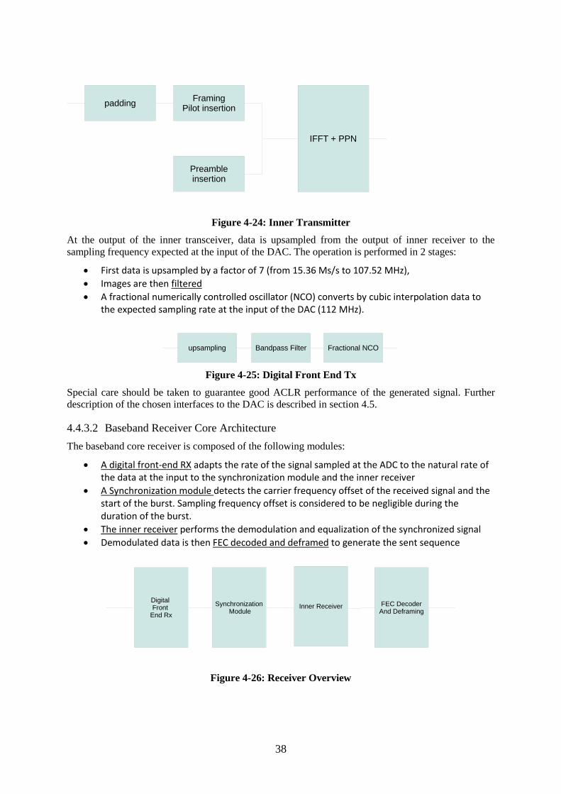
sampling frequency expected at the input of the DAC. The operation is performed in 2 stages:
First data is upsampled by a factor of 7 (from 15.36 Ms/s to 107.52 MHz),
Images are then filtered
A fractional numerically controlled oscillator (NCO) converts by cubic interpolation data to the expected sampling rate at the input of the DAC (112 MHz).
Figure 4-25: Digital Front End Tx
Special care should be taken to guarantee good ACLR performance of the generated signal. Further
description of the chosen interfaces to the DAC is described in section 4.5.
4.4.3.2 Baseband Receiver Core Architecture
The baseband core receiver is composed of the following modules:
A digital front-end RX adapts the rate of the signal sampled at the ADC to the natural rate of the data at the input to the synchronization module and the inner receiver
A Synchronization module detects the carrier frequency offset of the received signal and the start of the burst. Sampling frequency offset is considered to be negligible during the duration of the burst.
The inner receiver performs the demodulation and equalization of the synchronized signal
Demodulated data is then FEC decoded and deframed to generate the sent sequence
Figure 4-26: Receiver Overview
paddingFraming
Pilot insertion
Preambleinsertion
IFFT + PPN
upsampling Bandpass Filter Fractional NCO
Synchronization Module
Inner Receiver FEC DecoderAnd Deframing
Digital Front
End Rx

39
The receiver digital front end is composed of:
A rotor function that transforms the carrier modulated signal into I/Q baseband modulated signal and followed by a downsampling operation (by a factor 2, see section 4.5). Downsampling is preceded by a bandpass filter to avoid aliasing.
A Bandpass filter rmoves from the signal all possible aliasing
A Fractional NCO/Resampler resamples the generated signal to the appropriate sampling frequency by linear interpolation (15.36Msamples/s).
Figure 4-27: Digital Front End Rx
The receiver synchronization is estimated and applied:
The autocorrelation of the received signal allows for signal detection and carrier frequency offset (CFO) estimation
CFO is then applied to the received signal.
Figure 4-28: Receiver Synchronization
The inner receiver is at the core of the FBMC demodulator. For ease of implementation data is
demodulated using two instantiation of the FFT algorithm. A first path applies the FFT directly on the
received burst, while the other path applies the FFT on the delayed version of the received burst. Data
is then accumulated before operations of equalization and demapping. The equalizer estimates the
channel frequency response using the preamble. Since only every 4 carrier is active during the
preamble, channel estimated on the preamble is interpolated in frequency to estimate the channel on
every active carriers. Interpolation is realized using optimised Wiener filters. Then zero forcing (ZF)
equalization is applied on the data burst before demapping to generate log-likelihood ratio metrics at
the input to the FEC decoder.
Rotor I/QDownsampling
Bandpass Filter Fractional NCO
delay
Autocorrelation
CFOcorrection

40
Figure 4-29: Inner Receiver Architecture
Data is then de-interleaved, FEC decoded, blocks are then FEC de-segmented and de-scrambled.
Figure 4-30: Inner Receiver architecture
The data stream is then transfer via the OMAP GPMC interface to the ARM Cortex-A8
4.5 Transceiver Interfaces
4.5.1 RF Interface baseband TX and RX interface
As specified in section 4.2, a high IF of 280MHz has been chosen to relax the requirements of the pre-
selection filter. The choice of relatively high speed DAC and ADC for the baseband board has been
made such that conversion from intermediate frequency to inband and quadrature (or I/Q) signals is
realized in digital. This element is also a consequence of the flexible nature of the transceiver design.
Special attention is put to describe the consequences a relatively high IF would have on the baseband
design.
The QoSMOS board dispose of a quad 14-bit ADC providing a maximum sampling frequency of
250MHz and maximum bandwidth of 400MHz.
A subsampling architecture has therefore been considered, i.e. an architecture for which the sampling
frequency, fs, is smaller than the frequency of the useful signal. Subsampling on the first image has
been chosen and is given in Figure 4-31. The useful signal is around 280MHz and has a maximum
bandwidth of 40MHz. If the carrier frequency, fs, is larger than but smaller than 1.5 times the
sampling frequency, two images around fd1 and fd2 are to be at the output of the sampling process.
FFT
Filter
FFT
FilterDelay
Accu
Estimation decanal
Channel Estimation
Interpolation
ZFEqualization
Dmapping LLR
Deinterleaver
BCCDecoder
LDPCDecoder
FEC Desegmentation
Descrambler

41
Figure 4-31: First image subsampling
Table 4-6 gives some subsampling options at the ADC. Images are more or less separated from each
other depending on the sampling frequency. The sampling frequency that reduces the most the
constraints on the digital filter after digitization is found to be 224MHz. This is the option that has
been taken for the QosMOS design.
Table 4-6: Subsampling frequency options
Sampling Frequency (fs)
First Image (fd1)
Second Image (fd2)
Distance Between Images (delt1)
Distance between Images (delt2)
200MHz 80MHz 120MHz 0MHZ 120MHz
224MHz 56MHz 168MHz 72MHz 72MHz
Because of the very conservative requirement on the ACLR at the transmitter, the sampling frequency
of the DAC has been chosen as large as possible by the design. In order to reduce intermodulation
products between the ADC and the DAC, it was decided to use a multiple of the proposed 224MHz
ADC sampling frequency. The sampling frequency of 896MHz has therefore been chosen. This is 4
times 224MHz, but below the maximum sampling frequency specification of the 16-bit DAC of
1Gsample/s.
These relatively high frequencies for a digital design have made possible by the implementation of a
digital front-end for both the TX and the RX necessary.
Most of the digital design is therefore clocked at 112MHz (this is effectively half of the ADC
sampling frequency). While data generated by the modulation is expected to be processed at
15.36MHz, the actual design is clocked at a higher frequency in order to limit digital noise harmonics
feeding into the transmitted and received signals (see section 4.4.3).
At the transmitter, the DAC provided on board contains a built-in interpolation module with an
integrated NCO. Therefore the interface to the DAC is a baseband digital I/Q interface at 112MHz.
For the ADC, the interface runs at 224MHz and decimation and downconvertion is performed inside
the FPGA.
4.5.2 Baseband Digital Interface – Dynamic and Flexible parameters
The digital interface between the ARM Cortex-8 and the baseband FPGA is further described in this
section. Through the configuration manager a number of parameters may be set to allow for flexible
and dynamic update of the emitted and received waveforms. An extract of the table can be found in
Table 4-7, for a more complete set of the programmable parameters please refer to Appendix 8.1.
This table is an illustration of the flexible features of the baseband and RF transceiver. All these
registers may be accessed by the software interface. The most important features are described here
below. Registers are either input register (write / in ) or output registers (read / out). One important
Signal
(fc = 280 MHz)fs
fd1 fd20
delt1 delt2
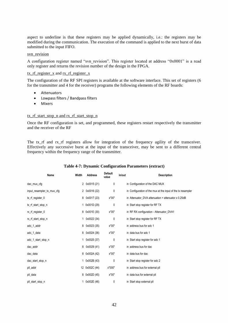
42
aspect to underline is that these registers may be applied dynamically, i.e.: the registers may be
modified during the communication. The execution of the command is applied to the next burst of data
submitted to the input FIFO.
svn_revision
A configuration register named “svn_revision”. This register located at address “0x0001” is a read
only register and returns the revision number of the design in the FPGA.
tx_rf_register_x and rx_rf_register_x
The configuration of the RF SPI registers is available at the software interface. This set of registers (6
for the transmitter and 4 for the receiver) programs the following elements of the RF boards:
Attenuators
Lowpass filters / Bandpass filters
Mixers
tx_rf_start_stop_n and rx_rf_start_stop_n
Once the RF configuration is set, and programmed, these registers restart respectively the transmitter
and the receiver of the RF
The tx_rf and rx_rf registers allow for integration of the frequency agility of the transceiver.
Effectively any successive burst at the input of the transceiver, may be sent to a different central
frequency within the frequency range of the transmitter.
Table 4-7: Dynamic Configuration Parameters (extract)
Name Width Address Default value
in/out Description
dac_mux_cfg 2 0x0015 (21) 0 in Configuration of the DAC MUX
input_resampler_tx_mux_cfg 2 0x0016 (22) 0 in Configuration of the mux at the input of the tx resampler
tx_rf_register_0 8 0x0017 (23) x"00" in Attenuator_DVA attenuation = attenuator x 0.25dB
tx_rf_start_stop_n 1 0x001D (29) 0 in Start stop register for RF TX
rx_rf_register_0 8 0x001E (30) x"00" in RF RX configuration - Attenuator_DVA1
rx_rf_start_stop_n 1 0x0022 (34) 0 in Start stop register for RF TX
adc_1_addr 8 0x0023 (35) x"00" in address bus for adc 1
adc_1_data 8 0x0024 (36) x"00" in data bus for adc 1
adc_1_start_stop_n 1 0x0025 (37) 0 in Start stop register for adc 1
dac_addr 8 0x0029 (41) x"00" in address bus for dac
dac_data 8 0x002A (42) x"00" in data bus for dac
dac_start_stop_n 1 0x002B (43) 0 in Start stop register for adc 2
pll_addr 12 0x002C (44) x"000" in address bus for external pll
pll_data 8 0x002D (45) x"00" in data bus for external pll
pll_start_stop_n 1 0x002E (46) 0 in Start stop external pll

43
scrambler_reg_init 16 0x002F (47) 0 in init value of the prbs register
bypass_scrambler 1 0x0030 (48) x"0" in bypass of the scrambler
bypass_interleaver 1 0x0031 (49) 0 in bypass of the interleaver
modulation 2 0x0032 (50) 0 in 0: QPSK 1:16-QAM 2:64-QAM 3: 256-QAM
fec_code_rate 2 0x0033 (51) 0 in 0: 1/2 1: 2/3 2: 3/4 3: 5/6
fec_type 2 0x0034 (52) x"0" in 0: None 1: CC 2: LDPC
fec_coding_size 12 0x0035 (53) 2304 in size of the output of the FEC
fec_input_size 12 0x0036 (54) 1144 in size of the input of the FEC ( padding exclude)
mask_pattern_1 6 0x0042 (66) x"0000" in Mask
mask_pattern_2 6 0x0043 (67) x"00FF" in Mask
mask_pattern_3 6 0x0044 (68) x"0001" in Mask
mask_active_carrier_pattern_1_0 32 0x0048 (72) x"00000000" in Mask
active_carrier_0 32 0x0108
(264) x"00000000" in Mask
svn_revision 16 0x0001 (1) n.a out SVN Revision
stream_out_0_nb_word_fifo_interface 32 0x0007 (7) n.a out Number of words ready to read in the stream 0 arm interface
stream_out_1_nb_word_fifo_interface 16 0x0009 (9) n.a out Number of words ready to read in the stream 1 arm interface
stream_out_0_overflow_fifo 1 0x000A (10) n.a out Overflow signal for stream 0 arm interface
rx_error_fifo_overflow_output_resampler 1 0x000C (12) n.a out The MSB indicates that an overflow occurs on the rx resampler fifo
adc_1_addr adc_1_data adc_1_start_stop_n
dac_addr dac_data dac_start_stop_n
pll_addr pll_data pll_start_stop_n
The analog-to-digital, digital-to-analog and the baseband phase locked loop may also be controlled,
started and stoped.
bypass_scrambler bypass_interleaver
Bypass features notably for the scrambler and the interleaver are available. There are usually useful for
debug purposes.
modulation fec_code_rate fec_type
The choice of the modulation may also be selected dynamically, QPSK, 16QAM, 64QAM and
256QAM are available. Various code rates and FEC types (No FEC, convolutional and LDPC) are
available.
mask_pattern_1 mask_pattern_2 mask_pattern_3 mask_active_carrier_pattern_1_0 active_carrier_0
This set of registers allows for flexible baseband features of the transceiver. The mask_pattern_x and
mask_active_carrier_pattern_x registers are registers that are set to define the preamble of the

44
transceiver, while active_carrier_x allows for the selection of the active carriers of the data part of the
burst. The preamble is composed of 3 possible patterns that are added and that are repeated in time and
masked. Register nb_preamble_symb sets the duration of the preambule in time, mask_pattern_<1-3>
sets when during the preamble the pattern_<1-3> should be activated and
mask_active_carrier_pattern<1-3>_<carrier> sets whether the carrier is active for that pattern. Data
used for this preamble is a generated by a Pseudo-Random-Bit-Sequence (PRBS) generator with a
seed that is programmable.
Figure 4-32: Flexible preamble generation
The generation of a flexible preamble pattern allows not only to adapt the pattern used for
synchronisation and channel estimation with the different transmission scenarios (e.g.: indoor short
range, fixed larger distance, ..), but also to adapt the pattern as a function of the occupancy of the
channel and support fragmented spectrum.
Therefore, the set of programmable registers, active_carrier_<0-31>, allows for flexible spectrum
pooling. Each available carrier of the multicarrier modulation may be activated or deactivated. Since
the implemented FBMC waveform presents a built-in filter that gives good ACLR performance using
the spectrum pooling technique in comparison to other multicarrier waveforms such as OFDM.
nb_preamble_symbAnd mask_pattern<1-3>
nb_preamble_symbAnd mask_pattern<1-3>
Resulting pattern
mask_active_
carr
ier_
patte
rn_<
1-3
>_<
carr
ier>

45
5 Performance of QoSMOS Flexible Transceiver
5.1 RF Transceiver Performance
The test board shown in Figure 5-1 was developed to measure the characteristics of the QoSMOS RF
front-end boards without requiring the baseband board. The test board provides the same connectors to
the RF board as the baseband board.
Figure 5-1: Test board implementation hosting a RF board
The results presented below were obtained from measurement of the RF boards excluding the digital
part. The quantities measured were determined by common measurement setups.
5.1.1 RF RX Board Measurement
5.1.1.1 IF Output Spectrum
Figure 5-2 shows the measured output spectrum of the RF RX board if a sine wave at 730 MHz is fed
at the input. The output frequency, i.e., the IF, is 280 MHz.

46
Figure 5-2: IF output spectrum measurement for 730MHz CW input signal
Figure 5-3 illustrates the IF output spectrum for an input signal swept from 700MHz to 760MHz. The
IF bandpass characteristic is clearly pronounced.
Figure 5-3: IF output spectrum sweep with frequency from 700 MHz to 760 MHz
5.1.1.2 Noise Figure
A screenshot of the noise figure measurement is shown in Figure 5-4, exemplarily depicting the
frequency response for an input frequency range of 695MHz to 745MHz. As seen, the noise figure
amounts to 3.5dB at most.
1 AP
CLRWR
A
*RBW 10 kHz
VBW 30 kHz
SWT 9 sRef 5 dBm
Start 100 MHz Stop 1 GHz90 MHz/
Att 25 dB*
-90
-80
-70
-60
-50
-40
-30
-20
-10
0
1
Marker 1 [T1 ]
-0.08 dBm
280.000000000 MHz
Date: 23.NOV.2012 16:50:20
A
Ref 30 dBm Att 60 dB
Center 280 MHz Span 100 MHz10 MHz/
*RBW 1 MHz
VBW 3 MHz
SWT 2.5 ms
1 AP
MAXH
*
-70
-60
-50
-40
-30
-20
-10
0
10
20
30
1
Marker 1 [T1 ]
0.70 dBm
280.000000000 MHz
2
Marker 2 [T1 ]
1.18 dBm
260.000000000 MHz
3
Marker 3 [T1 ]
1.00 dBm
300.000000000 MHz
Date: 31.OCT.2012 15:24:39
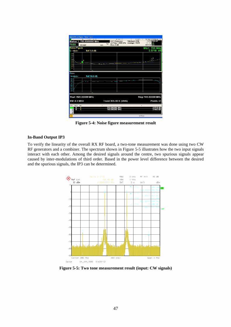
47
Figure 5-4: Noise figure measurement result
In-Band Output IP3
To verify the linearity of the overall RX RF board, a two-tone measurement was done using two CW
RF generators and a combiner. The spectrum shown in Figure 5-5 illustrates how the two input signals
interact with each other. Among the desired signals around the centre, two spurious signals appear
caused by inter-modulations of third order. Based in the power level difference between the desired
and the spurious signals, the IP3 can be determined.
Figure 5-5: Two tone measurement result (input: CW signals)

48
5.1.1.3 Phase Noise
Phase noise was measured over the whole chain at IF, feeding a signal at 720MHz at the RF input. The
phase noise of the signal depends on noise properties of the signal generator, which generates the input
signal, and the on-board synthesiser of the RF RX. Figure 5-6 illustrates the phase noise spectrum
along with the properties of the input and output signals.
Table 5-1: Phase noise measurement – Power levels
CW input level -30 dBm
CW input frequency 720 MHz
output level 5 dBm
output frequency 280 MHz
Figure 5-6: Phase noise spectrum for a 720MHz CW input signal
5.1.2 Measurement TX RF board
Figure 5-7 portrays the RF output spectrum measured at 720MHz for a sine wave IF signal.

49
Figure 5-7: RF output spectrum measurement at 720 MHz (CW IF signal)
5.2 Baseband and RF integrated Performance
The performance of the baseband transmitter and receiver has been tested and measured integrated
with the RF transmitter and receiver. The main performance concern came from the noise generated
by the digital components on the quality of the transmitter; another concern came from the linearity of
the mixed signal components and their influence on the frequency response of the FBMC waveform.
The dynamic range inside the digital design should also be validated.
Ref 10 dBm Att 40 dB
A
1 AP
CLRWR
5 MHz/Center 720 MHz Span 50 MHz
*RBW 3 kHz
SWT 5.6 s
*VBW 3 kHz
-90
-80
-70
-60
-50
-40
-30
-20
-10
0
10 1 Marker 1 [T1 ]
4.69 dBm
720.000000000 MHz
2
Marker 2 [T1 ]
-72.84 dBm
706.300000000 MHz
Date: 23.OCT.2012 17:13:12

50
Figure 5-8: RF output spectrum measurement at 720MHz for a sinewave generated by the
baseband board
A sinewave baseband signal generated by the baseband board and fed to the DAC gives a Spurious-
Free-Dynamic Range ( SFDR) to a level almost equal to 73dB. This is a comparable level to the level
obtained when the sinewave is generated by a sinewave generator (Figure 5-7). The signal is obtained
by generating a full amplitude sinewave at 280MHz by the onboard DAC. The signal is then
upconverted to 720MHz by the flexible transmitter. Most of the performance degradation in
comparison to a signal generated by a signal generator may be measured on the phase noise properties
that are degraded. This is due to the quality of the on-board oscillator, notably the oscillators used to
latch the DAC.
Similar level of performance has also been measured at 490MHz and at 650MHz.
A second set of measurement concerns the transmitter response to FBMC waveforms. An FBMC
waveform has been generated by an arbitrary waveform generator at an IF of 280MHz. The generated
signal is then fed through the RF Transmitter. ACLR performance is then measured.
1 AP
CLRWR
A
*RBW 3 kHz
VBW 10 kHz
SWT 11.5 sRef 10 dBm Att 40 dB
Center 720 MHz Span 100 MHz10 MHz/
-90
-80
-70
-60
-50
-40
-30
-20
-10
0
10
1
Marker 1 [T1 ]
7.72 dBm
720.000000000 MHz
2
Delta 2 [T1 ]
-75.78 dB
800.000000000 kHz
Date: 24.OCT.2012 10:56:33
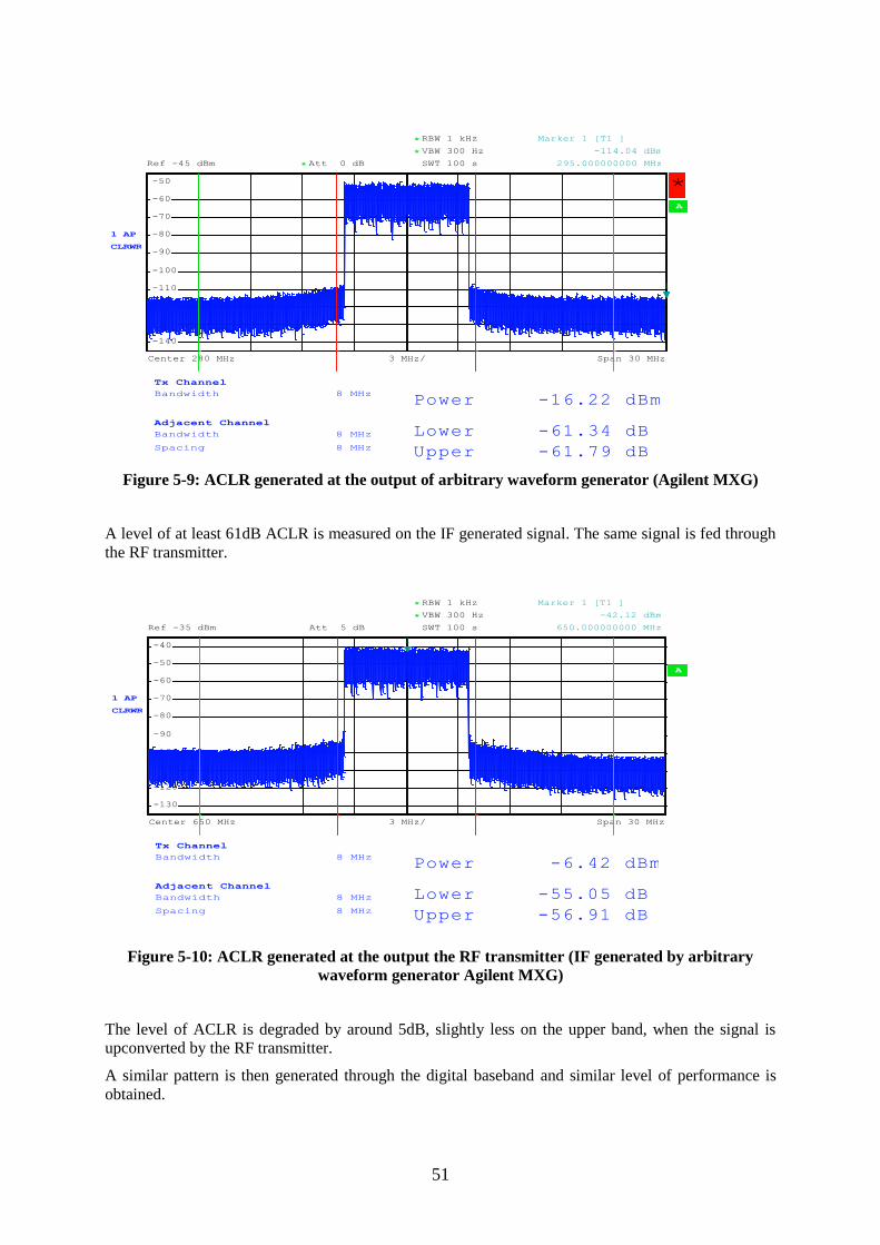
51
Figure 5-9: ACLR generated at the output of arbitrary waveform generator (Agilent MXG)
A level of at least 61dB ACLR is measured on the IF generated signal. The same signal is fed through
the RF transmitter.
Figure 5-10: ACLR generated at the output the RF transmitter (IF generated by arbitrary
waveform generator Agilent MXG)
The level of ACLR is degraded by around 5dB, slightly less on the upper band, when the signal is
upconverted by the RF transmitter.
A similar pattern is then generated through the digital baseband and similar level of performance is
obtained.
1 AP
CLRWR
A
*RBW 1 kHz
Att 0 dB*Ref -45 dBm
Center 280 MHz Span 30 MHz3 MHz/
*
*
VBW 300 Hz
SWT 100 s
-140
-130
-120
-110
-100
-90
-80
-70
-60
-50
Tx Channel
Bandwidth 8 MHz Power -16.22 dBm
Adjacent Channel
Bandwidth 8 MHz Lower -61.34 dB Spacing 8 MHz Upper -61.79 dB
1
Marker 1 [T1 ]
-114.04 dBm
295.000000000 MHz
Date: 24.OCT.2012 18:55:48
1 AP
CLRWR
A
Att 5 dBRef -35 dBm
Center 650 MHz Span 30 MHz3 MHz/
*RBW 1 kHz
*VBW 300 Hz
SWT 100 s
-130
-120
-110
-100
-90
-80
-70
-60
-50
-40
Tx Channel
Bandwidth 8 MHz Power -6.42 dBm
Adjacent Channel
Bandwidth 8 MHz Lower -55.05 dB Spacing 8 MHz Upper -56.91 dB
1
Marker 1 [T1 ]
-42.12 dBm
650.000000000 MHz
Date: 24.OCT.2012 18:49:20
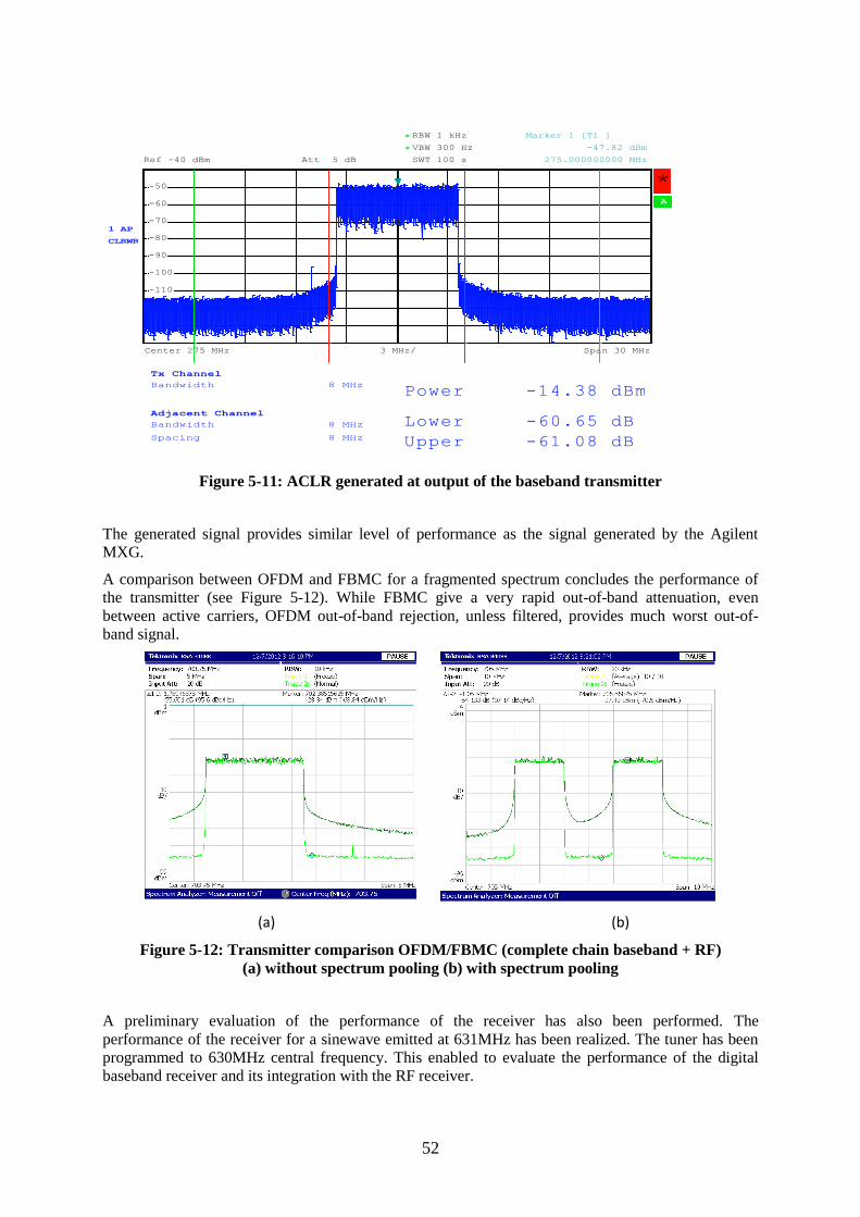
52
Figure 5-11: ACLR generated at output of the baseband transmitter
The generated signal provides similar level of performance as the signal generated by the Agilent
MXG.
A comparison between OFDM and FBMC for a fragmented spectrum concludes the performance of
the transmitter (see Figure 5-12). While FBMC give a very rapid out-of-band attenuation, even
between active carriers, OFDM out-of-band rejection, unless filtered, provides much worst out-of-
band signal.
(a) (b)
Figure 5-12: Transmitter comparison OFDM/FBMC (complete chain baseband + RF)
(a) without spectrum pooling (b) with spectrum pooling
A preliminary evaluation of the performance of the receiver has also been performed. The
performance of the receiver for a sinewave emitted at 631MHz has been realized. The tuner has been
programmed to 630MHz central frequency. This enabled to evaluate the performance of the digital
baseband receiver and its integration with the RF receiver.
Att 5 dB
1 AP
CLRWR
A
*RBW 1 kHz
*VBW 300 Hz
SWT 100 sRef -40 dBm
*
Center 275 MHz Span 30 MHz3 MHz/
-130
-120
-110
-100
-90
-80
-70
-60
-50
Tx Channel
Bandwidth 8 MHz Power -14.38 dBm
Adjacent Channel
Bandwidth 8 MHz Lower -60.65 dB Spacing 8 MHz Upper -61.08 dB
1
Marker 1 [T1 ]
-47.82 dBm
275.000000000 MHz
Date: 24.OCT.2012 20:27:13

53
(a) (b)
Figure 5-13: Received sinewave at the output of the digital front-end receiver
(Input sinewave at 631 MHz) – (a) I/Q versus time (b) Q versus I
The received signal is a sinewave centered at -1MHz.It gave a signal-to-noise ratio well above 40dB.
This meant that interaction between RF receiver and digital receiver performance degradation around
expected sensitivity level of -90dBm will not be dominated nor by ADC quantization effects, nor by
non-linearity effects in the receiver.
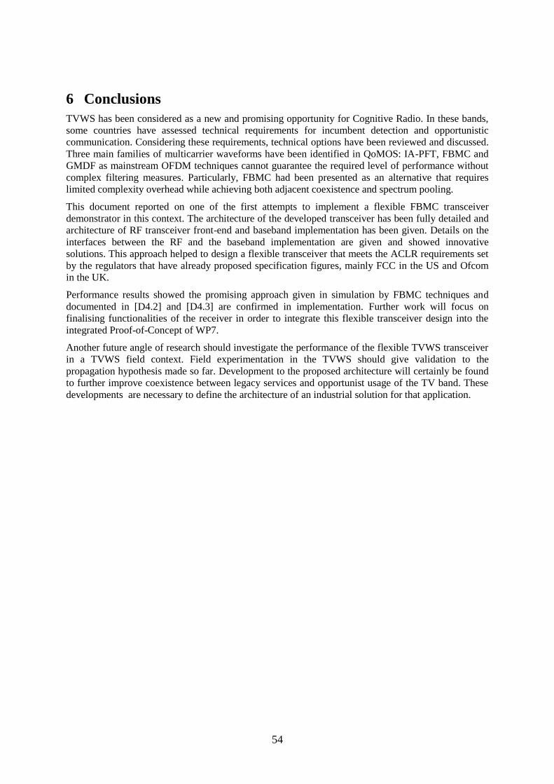
54
6 Conclusions
TVWS has been considered as a new and promising opportunity for Cognitive Radio. In these bands,
some countries have assessed technical requirements for incumbent detection and opportunistic
communication. Considering these requirements, technical options have been reviewed and discussed.
Three main families of multicarrier waveforms have been identified in QoMOS: IA-PFT, FBMC and
GMDF as mainstream OFDM techniques cannot guarantee the required level of performance without
complex filtering measures. Particularly, FBMC had been presented as an alternative that requires
limited complexity overhead while achieving both adjacent coexistence and spectrum pooling.
This document reported on one of the first attempts to implement a flexible FBMC transceiver
demonstrator in this context. The architecture of the developed transceiver has been fully detailed and
architecture of RF transceiver front-end and baseband implementation has been given. Details on the
interfaces between the RF and the baseband implementation are given and showed innovative
solutions. This approach helped to design a flexible transceiver that meets the ACLR requirements set
by the regulators that have already proposed specification figures, mainly FCC in the US and Ofcom
in the UK.
Performance results showed the promising approach given in simulation by FBMC techniques and
documented in [D4.2] and [D4.3] are confirmed in implementation. Further work will focus on
finalising functionalities of the receiver in order to integrate this flexible transceiver design into the
integrated Proof-of-Concept of WP7.
Another future angle of research should investigate the performance of the flexible TVWS transceiver
in a TVWS field context. Field experimentation in the TVWS should give validation to the
propagation hypothesis made so far. Development to the proposed architecture will certainly be found
to further improve coexistence between legacy services and opportunist usage of the TV band. These
developments are necessary to define the architecture of an industrial solution for that application.

55
7 References
[802.11af] IEEE 802.11af, TV white space study group af, Wireless Local Area
Network (WLAN), http://www.ieee802.org/11/
[802.22] IEEE 802.22, Wireless Regional Area Networks (“WRANs“),
http://www.ieee802.org/22/
[ANG12] The Ångström Distribution, http://www.angstrom-distribution.org
[BER11] V. Berg and D. Noguet, IEEE 1900.7 White Space Radio, ACLR issues
with OFDM for TVWS operation, 2011-12-12/14; Scottsdale, AZ
[BER12] V. Berg, D. Noguet and X. Popon, A Flexible Hardware Platform for
Mobile Cognitive Radio applications, Euromicro DSD, Cesme, Turkey
Sept. 2012.
[BIA09] L. Biard, D. Noguet, T. Gernandt, P. Marques, A. Gameiro. “A Hardware
Demonstrator of an Opportunistic Radio System Using Temporal
Opportunities”, Cognitive Radio Oriented Wireless Networks and
Communications (Crowncom), Hanover, Germany, 2009.
[CEPT09] Report from CEPT to the European Commission in response to the
Mandate on “The identification of common and minimal (least
restrictive) technical conditions for 790 - 862 MHz for the digital
dividend in the European Union”, CEPT report 30
http://www.erodocdb.dk/Docs/doc98/official/pdf/CEPTREP030.PDF,
October 2009.
[D1.3] FP7-ICT-2009-4/248454, QoSMOS Deliverable D1.3, QoSMOS initial
system requirements, Dec. 2010
[D2.3] FP7-ICT-2009-4/248454, QoSMOS Deliverable D2.4, System
specification and evaluation criteria, Dec. 2011
[D4.1] FP7-ICT-2009-4/248454, QoSMOS Deliverable D4.1, Transceiver
architectures and requirements, Aug. 2010
[D4.2] FP7-ICT-2009-4/248454, QoSMOS Deliverable D4.2, Flexible concepts
for white spaces – Intermediate Report, Dec. 2011
[D4.3] FP7-ICT-2009-4/248454, QoSMOS Deliverable D4.3, Flexible concepts
for white spaces – Final Report, Jun. 2012
[D7.2] FP7-ICT-2009-4/248454, QoSMOS Deliverable D7.2, QoSMOS
Platform Architecture Definition (2/2), to be submitted, Dec. 2011
[D7.3] FP7-ICT-2009-4/248454, QoSMOS Deliverable D7.3, QoSMOS
Prototype - version 1, Jun. 2012
[DVB09] ETSI EN 300 744, v1.6.1 (2009-01), Digital Video Broadcasting (DVB);
Framing structure, channel coding and modulation for digital terrestrial
television.
[DVB12] EN 302 755, v1.3.1 (04/12), Frame structure channel coding and
modulation for a second generation digital terrestrial television
broadcasting system (DVB-T2)
[ETS06] ETSI TR 102 546, v.1.1.1_1.0.3 (2006-12), Technical Report.

56
[FCC04] FCC proposed rule, “Unlicensed Operation in the TV Broadcast Bands”,
US Federal Register Vol. 69, No.117, pp 34103-34111, June 18 2004.
[FCC09] FCC final rule, “Unlicensed Operation in the TV Broadcast Bands”, US
Federal Register Vol. 74, No.30, pp 7314-7332, Feb. 17 2009
[FRE11] B. P. Freyens, M. Loney, “Opportunities for White Space Usage in
Australia”, 2nd International Conference on Wireless Communications,
Vehicular Technology, Information Theory and Aerospace in Electronic
Systems Technology (Wireless VITAE), Chennai, India, March 2011.
[JAE12] A. Jaschke, M. Tessema, M. Schühler, R. Wansch, „Digitally Tunable
Bandpass Filter for Cognitive Radio Applications”, in Proc. 2012 IEEE
17th International Workshop on Computer Aided Modeling and Design
of Communication Links and Networks (CAMAD), Barcelona (Spain),
Sep. 17-19, 2012.
[LEH12] P. H. Lehne, R. MacKenzie, D. Noguet, V. Berg, “Mapping Cognitive
Radio System Scenarios into the TVWS Context”, SDR’12 - WInnComm
– Europe, 27-29 June 2012, Bruxelles.
[MIS05] S. M. Mishra, D. Cabric, C. Chang, D. Willkomm, B. van Schewick, A.
Wolisz and R. W. Brodersen, “A Real Time Cognitive Radio Testbed for
Physical and Network level Experiments”, IEEE International
Symposium on New Frontiers in Dynamic Spectrum Access Networks
(DYSPAN), 2005.
[MIT00] J. Mitola, “Cognitive Radio: An Integrated Agent Architecture for
Software Defined Radio”, Ph.D. thesis, Royal Inst. Of Tech., Sweden,
May 2000.
[MIT95] J. Mitola, “The software Radio Architecture”, IEEE Communications
Magazine, May 95, pp.26-38..
[NEK10] Nekovee, M., “A Survey of Cognitive Radio Access to TVWhite
Spaces”, International Journal of Digital Multimedia Broadcasting,
Volume 2010, Hindawi
[NOG11] D. Noguet, M. Gautier and V. Berg, “Advances in Opportunistic Radio
Technologies for TVWS,” EURASIP Journal on Wireless
Communications and Networking 2011, 2011:170 doi:10.1186/1687-
1499-2011-170, Published: 15 November 2011
[OFC09] Digital dividend: cognitive access," Statement on licence exempting
cognitive devices using interleaved spectrum, July 2009
[ORAD3.3] D3.3 Advanced Transmitter Architectures for OR Terminals, Oracle,
2008
[PAW11] P. Pawelczak, K. Nolan, L. Doyle, S. W. Oh, D. Cabric, “Cognitive
Radio: Ten Years of Experimentation and Developmnet”, IEEE
Communications Magazine, March 2011
[RAY05] D. Raychaudhuri, I. Seskar, M. Ott, S. Ganu, K. Ramachandran, H.
Kremo, R. Siracusa, H. Liu and M. Singh, “Overview of the ORBIT
Radio Grid Testbed for Evaluation of Next-Generation Wireless Network
Protocols”, IEEE Wireless Communications and Networking Conference
(WCNC), 2005
57
[TI10] Texas Instruments AM/DM37xx Overview,
http://processors.wiki.ti.com/index.php/AM/DM37x_Overview
[WEI04] T. A. Weiss, F. K. Jondral, "Spectrum pooling: an innovative strategy for
the enhancement of spectrum efficiency", IEEE Communications
Magazine, vol. 42, no. 3, pp.S8-S14, March 2004.
[YEO08] Yeoh, W.S.; Wong, K.L.; Rowe, W.S.T.; "Miniaturized Half-Bowtie
Printed Dipole Antenna with an Integrated Balun," Microwave
Conference, 2008. APMC 2008. Asia-Pacific , vol., no., pp.1-4, 16-20
Dec. 2008

58
8 Appendices
8.1 Flexible Interface between ARM and FPGA
This appendix gives the complete list of programmable registers in the FPGA design
Table 8-1: Dynamic Configuration Parameters
Name Width Address Default value
in/out Description
data_write_stream_out 16 0x000D (13) 0 in This register is pluigged to the stream 0 output mux interface
stream_out_0_start_stop_n 1 0x000E (14) 0 in Activataion of the output stream 0 interface
stream_out_1_start_stop_n 1 0x000F (15) 0 in Activataion of the output stream 1 interface
stream_out_0_nb_data_acqui 32 0x0010 (16) 0 in It specifies the number of data to read at the output stream 0 interface (0: no limit)
stream_out_1_nb_data_acqui 16 0x0012 (18) 0 in It specifies the number of data to read at the output stream 1 interface (0: no limit)
stream_out_0_mux 4 0x0013 (19) 0 in It sepfifies which data are dumped at stream out 0 interface (TBD)
stream_out_1_mux 4 0x0014 (20) 0 in It sepfifies which data are dumped at stream out 1 interface (TBD)
dac_mux_cfg 2 0x0015 (21) 0 in Configuration of the DAC MUX
input_resampler_tx_mux_cfg 2 0x0016 (22) 0 in Configuration of the mux at the input of the tx resampler
tx_rf_register_0 8 0x0017 (23) x"00" in Attenuator_DVA attenuation = attenuator x 0.25dB
tx_rf_register_1 8 0x0018 (24) x"00" in RF TX configuration - not used
tx_rf_register_2 8 0x0019 (25) x"08" in RF TX configuration - Filter_LPF (DTC_TPF)
tx_rf_register_3 8 0x001A (26) x"04" in RF TX configuration - Filter_BPF (DTC)
tx_rf_register_4 8 0x001B (27) x"00" in RF TX configuration - Mixer_addr
tx_rf_register_5 16 0x001C (28) x"0000" in RF TX configuration - Mixer_data
tx_rf_start_stop_n 1 0x001D (29) 0 in Start stop register for RF TX
rx_rf_register_0 8 0x001E (30) x"00" in RF RX configuration - Attenuator_DVA1
rx_rf_register_1 8 0x001F (31) x"00" in RF RX configuration - Attenuator_DVA2
rx_rf_register_2 8 0x0020 (32) x"08" in RF RX configuration - Filter_LPF
rx_rf_register_3 8 0x0021 (33) x"04" in RF RX configuration - Filter_BPF
rx_rf_start_stop_n 1 0x0022 (34) 0 in Start stop register for RF TX
adc_1_addr 8 0x0023 (35) x"00" in address bus for adc 1
adc_1_data 8 0x0024 (36) x"00" in data bus for adc 1
adc_1_start_stop_n 1 0x0025 (37) 0 in Start stop register for adc 1
adc_2_addr 8 0x0026 (38) x"00" in address bus for adc 2

59
adc_2_data 8 0x0027 (39) x"00" in data bus for adc 2
adc_2_start_stop_n 1 0x0028 (40) 0 in Start stop register for adc 2
dac_addr 8 0x0029 (41) x"00" in address bus for dac
dac_data 8 0x002A (42) x"00" in data bus for dac
dac_start_stop_n 1 0x002B (43) 0 in Start stop register for adc 2
pll_addr 12 0x002C (44) x"000" in address bus for external pll
pll_data 8 0x002D (45) x"00" in data bus for external pll
pll_start_stop_n 1 0x002E (46) 0 in Start stop external pll
scrambler_reg_init 16 0x002F (47) 0 in init value of the prbs register
bypass_scrambler 1 0x0030 (48) x"0" in bypass of the scrambler
bypass_interleaver 1 0x0031 (49) 0 in bypass of the interleaver
modulation 2 0x0032 (50) 0 in 0: QPSK 1:16-QAM 2:64-QAM 3: 256-QAM
fec_code_rate 2 0x0033 (51) 0 in 0: 1/2 1: 2/3 2: 3/4 3: 5/6
fec_type 2 0x0034 (52) x"0" in 0: None 1: CC 2: LDPC
fec_coding_size 12 0x0035 (53) 2304 in size of the output of the FEC
fec_input_size 12 0x0036 (54) 1144 in size of the input of the FEC ( padding exclude)
nb_coding_block 16 0x0037 (55) 64 in number of coded block
nb_fft 10 0x0038 (56) 1023 in number of FFT required to send all the data
nb_pading_bit 13 0x0039 (57) 20 in number of bits required for padding fft
nb_active_carriers 10 0x003A (58) 489 in number of active carriers
norm_factor_re_pattern_1 12 0x003B (59) 0 in FIXME
norm_factor_im_pattern_1 12 0x003C (60) 0 in FIXME
norm_factor_re_pattern_2 12 0x003D (61) 0 in FIXME
norm_factor_im_pattern_2 12 0x003E (62) 0 in FIXME
norm_factor_re_pattern_3 12 0x003F (63) 0 in FIXME
norm_factor_im_pattern_3 12 0x0040 (64) 0 in FIXME
nb_preamble_symb 3 0x0041 (65) 4 in Number of preamble symbol
mask_pattern_1 6 0x0042 (66) x"0000" in Mask
mask_pattern_2 6 0x0043 (67) x"00FF" in Mask
mask_pattern_3 6 0x0044 (68) x"0001" in Mask
reg_init_prbs_1 16 0x0045 (69) x"0000" in PRBS register initialization
reg_init_prbs_2 16 0x0046 (70) x"5119" in PRBS register initialization
reg_init_prbs_3 16 0x0047 (71) x"5118" in PRBS register initialization
mask_active_carrier_pattern_1_0 32 0x0048 (72) x"00000000" in Mask
mask_active_carrier_pattern_1_1 32 0x004A (74) x"00000000" in Mask
mask_active_carrier_pattern_1_2 32 0x004C (76) x"00000000" in Mask

60
mask_active_carrier_pattern_1_3 32 0x004E (78) x"00000000" in Mask
mask_active_carrier_pattern_1_4 32 0x0050 (80) x"00000000" in Mask
mask_active_carrier_pattern_1_5 32 0x0052 (82) x"00000000" in Mask
mask_active_carrier_pattern_1_6 32 0x0054 (84) x"00000000" in Mask
mask_active_carrier_pattern_1_7 32 0x0056 (86) x"00000000" in Mask
mask_active_carrier_pattern_1_8 32 0x0058 (88) x"00000000" in Mask
mask_active_carrier_pattern_1_9 32 0x005A (90) x"00000000" in Mask
mask_active_carrier_pattern_1_10 32 0x005C (92) x"00000000" in Mask
mask_active_carrier_pattern_1_11 32 0x005E (94) x"00000000" in Mask
mask_active_carrier_pattern_1_12 32 0x0060 (96) x"00000000" in Mask
mask_active_carrier_pattern_1_13 32 0x0062 (98) x"00000000" in Mask
mask_active_carrier_pattern_1_14 32 0x0064
(100) x"00000000" in Mask
mask_active_carrier_pattern_1_15 32 0x0066
(102) x"00000000" in Mask
mask_active_carrier_pattern_1_16 32 0x0068
(104) x"00000000" in Mask
mask_active_carrier_pattern_1_17 32 0x006A
(106) x"00000000" in Mask
mask_active_carrier_pattern_1_18 32 0x006C
(108) x"00000000" in Mask
mask_active_carrier_pattern_1_19 32 0x006E
(110) x"00000000" in Mask
mask_active_carrier_pattern_1_20 32 0x0070
(112) x"00000000" in Mask
mask_active_carrier_pattern_1_21 32 0x0072
(114) x"00000000" in Mask
mask_active_carrier_pattern_1_22 32 0x0074
(116) x"00000000" in Mask
mask_active_carrier_pattern_1_23 32 0x0076
(118) x"00000000" in Mask
mask_active_carrier_pattern_1_24 32 0x0078
(120) x"00000000" in Mask
mask_active_carrier_pattern_1_25 32 0x007A
(122) x"00000000" in Mask
mask_active_carrier_pattern_1_26 32 0x007C
(124) x"00000000" in Mask
mask_active_carrier_pattern_1_27 32 0x007E
(126) x"00000000" in Mask
mask_active_carrier_pattern_1_28 32 0x0080
(128) x"00000000" in Mask
mask_active_carrier_pattern_1_29 32 0x0082
(130) x"00000000" in Mask
mask_active_carrier_pattern_1_30 32 0x0084
(132) x"00000000" in Mask

61
mask_active_carrier_pattern_1_31 32 0x0086
(134) x"00000000" in Mask
mask_active_carrier_pattern_2_0 32 0x0088
(136) x"00000000" in Mask
mask_active_carrier_pattern_2_1 32 0x008A
(138) x"00000000" in Mask
mask_active_carrier_pattern_2_2 32 0x008C
(140) x"00000000" in Mask
mask_active_carrier_pattern_2_3 32 0x008E
(142) x"00000000" in Mask
mask_active_carrier_pattern_2_4 32 0x0090
(144) x"00000000" in Mask
mask_active_carrier_pattern_2_5 32 0x0092
(146) x"00000000" in Mask
mask_active_carrier_pattern_2_6 32 0x0094
(148) x"00000000" in Mask
mask_active_carrier_pattern_2_7 32 0x0096
(150) x"00000000" in Mask
mask_active_carrier_pattern_2_8 32 0x0098
(152) x"00000000" in Mask
mask_active_carrier_pattern_2_9 32 0x009A
(154) x"00000000" in Mask
mask_active_carrier_pattern_2_10 32 0x009C
(156) x"00000000" in Mask
mask_active_carrier_pattern_2_11 32 0x009E
(158) x"00000000" in Mask
mask_active_carrier_pattern_2_12 32 0x00A0
(160) x"00000000" in Mask
mask_active_carrier_pattern_2_13 32 0x00A2
(162) x"00000000" in Mask
mask_active_carrier_pattern_2_14 32 0x00A4
(164) x"00000000" in Mask
mask_active_carrier_pattern_2_15 32 0x00A6
(166) x"00000000" in Mask
mask_active_carrier_pattern_2_16 32 0x00A8
(168) x"00000000" in Mask
mask_active_carrier_pattern_2_17 32 0x00AA
(170) x"00000000" in Mask
mask_active_carrier_pattern_2_18 32 0x00AC
(172) x"00000000" in Mask
mask_active_carrier_pattern_2_19 32 0x00AE
(174) x"00000000" in Mask
mask_active_carrier_pattern_2_20 32 0x00B0
(176) x"00000000" in Mask
mask_active_carrier_pattern_2_21 32 0x00B2
(178) x"00000000" in Mask
mask_active_carrier_pattern_2_22 32 0x00B4
(180) x"00000000" in Mask

62
mask_active_carrier_pattern_2_23 32 0x00B6
(182) x"00000000" in Mask
mask_active_carrier_pattern_2_24 32 0x00B8
(184) x"00000000" in Mask
mask_active_carrier_pattern_2_25 32 0x00BA
(186) x"00000000" in Mask
mask_active_carrier_pattern_2_26 32 0x00BC
(188) x"00000000" in Mask
mask_active_carrier_pattern_2_27 32 0x00BE
(190) x"00000000" in Mask
mask_active_carrier_pattern_2_28 32 0x00C0
(192) x"00000000" in Mask
mask_active_carrier_pattern_2_29 32 0x00C2
(194) x"00000000" in Mask
mask_active_carrier_pattern_2_30 32 0x00C4
(196) x"00000000" in Mask
mask_active_carrier_pattern_2_31 32 0x00C6
(198) x"00000000" in Mask
mask_active_carrier_pattern_3_0 32 0x00C8
(200) x"00000000" in Mask
mask_active_carrier_pattern_3_1 32 0x00CA
(202) x"00000000" in Mask
mask_active_carrier_pattern_3_2 32 0x00CC
(204) x"00000000" in Mask
mask_active_carrier_pattern_3_3 32 0x00CE
(206) x"00000000" in Mask
mask_active_carrier_pattern_3_4 32 0x00D0
(208) x"00000000" in Mask
mask_active_carrier_pattern_3_5 32 0x00D2
(210) x"00000000" in Mask
mask_active_carrier_pattern_3_6 32 0x00D4
(212) x"00000000" in Mask
mask_active_carrier_pattern_3_7 32 0x00D6
(214) x"00000000" in Mask
mask_active_carrier_pattern_3_8 32 0x00D8
(216) x"00000000" in Mask
mask_active_carrier_pattern_3_9 32 0x00DA
(218) x"00000000" in Mask
mask_active_carrier_pattern_3_10 32 0x00DC
(220) x"00000000" in Mask
mask_active_carrier_pattern_3_11 32 0x00DE
(222) x"00000000" in Mask
mask_active_carrier_pattern_3_12 32 0x00E0
(224) x"00000000" in Mask
mask_active_carrier_pattern_3_13 32 0x00E2
(226) x"00000000" in Mask
mask_active_carrier_pattern_3_14 32 0x00E4
(228) x"00000000" in Mask

63
mask_active_carrier_pattern_3_15 32 0x00E6
(230) x"00000000" in Mask
mask_active_carrier_pattern_3_16 32 0x00E8
(232) x"00000000" in Mask
mask_active_carrier_pattern_3_17 32 0x00EA
(234) x"00000000" in Mask
mask_active_carrier_pattern_3_18 32 0x00EC
(236) x"00000000" in Mask
mask_active_carrier_pattern_3_19 32 0x00EE
(238) x"00000000" in Mask
mask_active_carrier_pattern_3_20 32 0x00F0
(240) x"00000000" in Mask
mask_active_carrier_pattern_3_21 32 0x00F2
(242) x"00000000" in Mask
mask_active_carrier_pattern_3_22 32 0x00F4
(244) x"00000000" in Mask
mask_active_carrier_pattern_3_23 32 0x00F6
(246) x"00000000" in Mask
mask_active_carrier_pattern_3_24 32 0x00F8
(248) x"00000000" in Mask
mask_active_carrier_pattern_3_25 32 0x00FA
(250) x"00000000" in Mask
mask_active_carrier_pattern_3_26 32 0x00FC
(252) x"00000000" in Mask
mask_active_carrier_pattern_3_27 32 0x00FE
(254) x"00000000" in Mask
mask_active_carrier_pattern_3_28 32 0x0100
(256) x"00000000" in Mask
mask_active_carrier_pattern_3_29 32 0x0102
(258) x"00000000" in Mask
mask_active_carrier_pattern_3_30 32 0x0104
(260) x"00000000" in Mask
mask_active_carrier_pattern_3_31 32 0x0106
(262) x"00000000" in Mask
active_carrier_0 32 0x0108
(264) x"00000000" in Mask
active_carrier_1 32 0x010A
(266) x"00000000" in Mask
active_carrier_2 32 0x010C
(268) x"00000000" in Mask
active_carrier_3 32 0x010E
(270) x"00000000" in Mask
active_carrier_4 32 0x0110
(272) x"00000000" in Mask
active_carrier_5 32 0x0112
(274) x"00000000" in Mask
active_carrier_6 32 0x0114
(276) x"00000000" in Mask

64
active_carrier_7 32 0x0116
(278) x"00000000" in Mask
active_carrier_8 32 0x0118
(280) x"00000000" in Mask
active_carrier_9 32 0x011A
(282) x"00000000" in Mask
active_carrier_10 32 0x011C
(284) x"00000000" in Mask
active_carrier_11 32 0x011E
(286) x"00000000" in Mask
active_carrier_12 32 0x0120
(288) x"00000000" in Mask
active_carrier_13 32 0x0122
(290) x"00000000" in Mask
active_carrier_14 32 0x0124
(292) x"00000000" in Mask
active_carrier_15 32 0x0126
(294) x"00000000" in Mask
active_carrier_16 32 0x0128
(296) x"00000000" in Mask
active_carrier_17 32 0x012A
(298) x"00000000" in Mask
active_carrier_18 32 0x012C
(300) x"00000000" in Mask
active_carrier_19 32 0x012E
(302) x"00000000" in Mask
active_carrier_20 32 0x0130
(304) x"00000000" in Mask
active_carrier_21 32 0x0132
(306) x"00000000" in Mask
active_carrier_22 32 0x0134
(308) x"00000000" in Mask
active_carrier_23 32 0x0136
(310) x"00000000" in Mask
active_carrier_24 32 0x0138
(312) x"00000000" in Mask
active_carrier_25 32 0x013A
(314) x"00000000" in Mask
active_carrier_26 32 0x013C
(316) x"00000000" in Mask
active_carrier_27 32 0x013E
(318) x"00000000" in Mask
active_carrier_28 32 0x0140
(320) x"00000000" in Mask
active_carrier_29 32 0x0142
(322) x"00000000" in Mask
active_carrier_30 32 0x0144
(324) x"00000000" in Mask

65
active_carrier_31 32 0x0146
(326) x"00000000" in Mask
mu 32 0x0148
(328) x"00000000" in Resampling factor
mux_output_tx 2 0x014A
(330) x"00" in configuration of the output TX MUX (0=> ROM)
frequency_sin_rom 14 0x014B
(331) x"0001" in Frequency of the generated sinus
. . . . . .
svn_revision 16 0x0001 (1) n.a out SVN Revision
througput_peak_write_config_register_fifo 16 0x0002 (2) n.a out Number max of word used in the fifo
througput_peak_stream_in_0_fifo 16 0x0003 (3) n.a out Number max of word used in the fifo
througput_peak_stream_in_1_fifo 16 0x0004 (4) n.a out Number max of word used in the fifo
througput_peak_stream_out_0_fifo 16 0x0005 (5) n.a out Number max of word used in the fifo
througput_peak_stream_out_1_fifo 16 0x0006 (6) n.a out Number max of word used in the fifo
stream_out_0_nb_word_fifo_interface 32 0x0007 (7) n.a out Number of words ready to read in the stream 0 arm interface
stream_out_1_nb_word_fifo_interface 16 0x0009 (9) n.a out Number of words ready to read in the stream 1 arm interface
stream_out_0_overflow_fifo 1 0x000A (10) n.a out Overflow signal for stream 0 arm interface
stream_out_1_overflow_fifo 1 0x000B (11) n.a out Overflow signal for stream 1 arm interface
rx_error_fifo_overflow_output_resampler 1 0x000C (12) n.a out The MSB indicates that an overflow occurs on the rx resampler fifo