Qorivva MPC5675K Microcontroller- Data Sheet · advanced driver assistance systems with RADAR, ......
147
TBD QFN12 ##_mm_x_##mm ##_mm_x_##mm PKG-TBD ## mm x ## mm 257 MAPBGA (14 x 14 mm) 473 MAPBGA (19 x 19 mm) Freescale Semiconductor Data Sheet: Technical Data Document Number: MPC5675K Rev. 8, 10/2013 MPC5675K © Freescale Semiconductor, Inc., 2009–2013. All rights reserved. 1 Introduction 1.1 Document overview This document provides electrical specifications, pin assignments, and package diagrams for the Qorivva MPC5675K series of microcontroller units (MCUs). 1.2 Description The Qorivva MPC5675K microcontroller, a SafeAssure solution, is a 32-bit embedded controller designed for advanced driver assistance systems with RADAR, CMOS imaging, LIDAR and ultrasonic sensors, and multiple 3-phase motor control applications as in hybrid electric vehicles (HEV) in automotive and high temperature industrial applications. A member of Freescale Semiconductor’s Qorivva MPC5500/5600 family, it contains the Book E compliant Power Architecture technology core with Variable Length Encoding (VLE). This core complies with the Power Architecture embedded category, and is 100 percent user mode compatible with the original Power PC user instruction set architecture (UISA). It offers system performance up to four times that of its MPC5561 predecessor, while bringing you the reliability and familiarity of the proven Power Architecture technology. A comprehensive suite of hardware and software development tools is available to help simplify and speed system design. Development support is available from leading tools vendors providing compilers, debuggers and simulation development environments. 1 Introduction . . . . . . . . . . . . . . . . . . . . . . . . . . . . . . . . . . . . . . . 1 1.1 Document overview . . . . . . . . . . . . . . . . . . . . . . . . . . . . 1 1.2 Description . . . . . . . . . . . . . . . . . . . . . . . . . . . . . . . . . . . 1 1.3 Device comparison . . . . . . . . . . . . . . . . . . . . . . . . . . . . . 3 1.4 Block diagram. . . . . . . . . . . . . . . . . . . . . . . . . . . . . . . . . 6 1.5 Feature list . . . . . . . . . . . . . . . . . . . . . . . . . . . . . . . . . . . 7 1.6 Feature details . . . . . . . . . . . . . . . . . . . . . . . . . . . . . . . . 8 2 Package pinouts and signal descriptions . . . . . . . . . . . . . . . . 18 2.1 Package pinouts . . . . . . . . . . . . . . . . . . . . . . . . . . . . . . 18 2.2 Pin descriptions . . . . . . . . . . . . . . . . . . . . . . . . . . . . . . 21 3 Electrical characteristics. . . . . . . . . . . . . . . . . . . . . . . . . . . . . 70 3.1 Introduction. . . . . . . . . . . . . . . . . . . . . . . . . . . . . . . . . . 70 3.2 Absolute maximum ratings . . . . . . . . . . . . . . . . . . . . . . 70 3.3 Recommended operating conditions . . . . . . . . . . . . . . 71 3.4 Thermal characteristics . . . . . . . . . . . . . . . . . . . . . . . . 73 3.5 Electromagnetic interference (EMI) characteristics . . . 74 3.6 Electrostatic discharge (ESD) characteristics. . . . . . . . 75 3.7 Static latch-up (LU) . . . . . . . . . . . . . . . . . . . . . . . . . . . . 75 3.8 Power Management Controller (PMC) electrical characteristics . . . . . . . . . . . . . . . . . . . . . . . . . . . . . 76 3.9 Supply current characteristics . . . . . . . . . . . . . . . . . . . 77 3.10 Temperature sensor electrical characteristics . . . . . . . 78 3.11 Main oscillator electrical characteristics . . . . . . . . . . . . 78 3.12 FMPLL electrical characteristics . . . . . . . . . . . . . . . . . . 79 3.13 16 MHz RC oscillator electrical characteristics. . . . . . . 80 3.14 ADC electrical characteristics . . . . . . . . . . . . . . . . . . . . 81 3.15 Flash memory electrical characteristics . . . . . . . . . . . . 86 3.16 SRAM memory electrical characteristics . . . . . . . . . . . 88 3.17 GP pads specifications . . . . . . . . . . . . . . . . . . . . . . . . . 88 3.18 PDI pads specifications . . . . . . . . . . . . . . . . . . . . . . . . 91 3.19 DRAM pad specifications . . . . . . . . . . . . . . . . . . . . . . . 94 3.20 RESET characteristics . . . . . . . . . . . . . . . . . . . . . . . . 101 3.21 Reset sequence . . . . . . . . . . . . . . . . . . . . . . . . . . . . . 101 3.22 Peripheral timing characteristics. . . . . . . . . . . . . . . . . 108 4 Package characteristics . . . . . . . . . . . . . . . . . . . . . . . . . . . . 132 4.1 Package mechanical data . . . . . . . . . . . . . . . . . . . . . 132 5 Orderable parts . . . . . . . . . . . . . . . . . . . . . . . . . . . . . . . . . . 138 6 Reference documents . . . . . . . . . . . . . . . . . . . . . . . . . . . . . 138 7 Document revision history . . . . . . . . . . . . . . . . . . . . . . . . . . 138 Qorivva MPC5675K Microcontroller Data Sheet
Transcript of Qorivva MPC5675K Microcontroller- Data Sheet · advanced driver assistance systems with RADAR, ......

TBD
MAPBGA–22515 mm x 15 mm
QFN12##_mm_x_##mm
SOT-343R##_mm_x_##mm
PKG-TBD## mm x ## mm
257 MAPBGA(14 x 14 mm)
473 MAPBGA(19 x 19 mm)
Freescale SemiconductorData Sheet: Technical Data
Document Number: MPC5675KRev. 8, 10/2013
MPC5675K
© Freescale Semiconductor, Inc., 2009–2013. All rights reserved.
1 Introduction
1.1 Document overviewThis document provides electrical specifications, pin assignments, and package diagrams for the Qorivva MPC5675K series of microcontroller units (MCUs).
1.2 DescriptionThe Qorivva MPC5675K microcontroller, a SafeAssure solution, is a 32-bit embedded controller designed for advanced driver assistance systems with RADAR, CMOS imaging, LIDAR and ultrasonic sensors, and multiple 3-phase motor control applications as in hybrid electric vehicles (HEV) in automotive and high temperature industrial applications.
A member of Freescale Semiconductor’s Qorivva MPC5500/5600 family, it contains the Book E compliant Power Architecture technology core with Variable Length Encoding (VLE). This core complies with the Power Architecture embedded category, and is 100 percent user mode compatible with the original Power PC user instruction set architecture (UISA). It offers system performance up to four times that of its MPC5561 predecessor, while bringing you the reliability and familiarity of the proven Power Architecture technology.
A comprehensive suite of hardware and software development tools is available to help simplify and speed system design. Development support is available from leading tools vendors providing compilers, debuggers and simulation development environments.
1 Introduction . . . . . . . . . . . . . . . . . . . . . . . . . . . . . . . . . . . . . . . 11.1 Document overview . . . . . . . . . . . . . . . . . . . . . . . . . . . . 11.2 Description . . . . . . . . . . . . . . . . . . . . . . . . . . . . . . . . . . . 11.3 Device comparison . . . . . . . . . . . . . . . . . . . . . . . . . . . . . 31.4 Block diagram. . . . . . . . . . . . . . . . . . . . . . . . . . . . . . . . . 61.5 Feature list . . . . . . . . . . . . . . . . . . . . . . . . . . . . . . . . . . . 71.6 Feature details . . . . . . . . . . . . . . . . . . . . . . . . . . . . . . . . 8
2 Package pinouts and signal descriptions . . . . . . . . . . . . . . . . 182.1 Package pinouts . . . . . . . . . . . . . . . . . . . . . . . . . . . . . . 182.2 Pin descriptions . . . . . . . . . . . . . . . . . . . . . . . . . . . . . . 21
3 Electrical characteristics. . . . . . . . . . . . . . . . . . . . . . . . . . . . . 703.1 Introduction. . . . . . . . . . . . . . . . . . . . . . . . . . . . . . . . . . 703.2 Absolute maximum ratings . . . . . . . . . . . . . . . . . . . . . . 703.3 Recommended operating conditions . . . . . . . . . . . . . . 713.4 Thermal characteristics . . . . . . . . . . . . . . . . . . . . . . . . 733.5 Electromagnetic interference (EMI) characteristics . . . 743.6 Electrostatic discharge (ESD) characteristics. . . . . . . . 753.7 Static latch-up (LU) . . . . . . . . . . . . . . . . . . . . . . . . . . . . 753.8 Power Management Controller (PMC) electrical characteristics . . . . . . . . . . . . . . . . . . . . . . . . . . . . . 763.9 Supply current characteristics . . . . . . . . . . . . . . . . . . . 773.10 Temperature sensor electrical characteristics . . . . . . . 783.11 Main oscillator electrical characteristics . . . . . . . . . . . . 783.12 FMPLL electrical characteristics. . . . . . . . . . . . . . . . . . 793.13 16 MHz RC oscillator electrical characteristics. . . . . . . 803.14 ADC electrical characteristics. . . . . . . . . . . . . . . . . . . . 813.15 Flash memory electrical characteristics . . . . . . . . . . . . 863.16 SRAM memory electrical characteristics . . . . . . . . . . . 883.17 GP pads specifications . . . . . . . . . . . . . . . . . . . . . . . . . 883.18 PDI pads specifications . . . . . . . . . . . . . . . . . . . . . . . . 913.19 DRAM pad specifications . . . . . . . . . . . . . . . . . . . . . . . 943.20 RESET characteristics . . . . . . . . . . . . . . . . . . . . . . . . 1013.21 Reset sequence . . . . . . . . . . . . . . . . . . . . . . . . . . . . . 1013.22 Peripheral timing characteristics. . . . . . . . . . . . . . . . . 108
4 Package characteristics . . . . . . . . . . . . . . . . . . . . . . . . . . . . 1324.1 Package mechanical data . . . . . . . . . . . . . . . . . . . . . 132
5 Orderable parts . . . . . . . . . . . . . . . . . . . . . . . . . . . . . . . . . . 1386 Reference documents . . . . . . . . . . . . . . . . . . . . . . . . . . . . . 1387 Document revision history . . . . . . . . . . . . . . . . . . . . . . . . . . 138
Qorivva MPC5675K Microcontroller Data Sheet

MPC5675K Microcontroller Data Sheet, Rev. 8
Introduction
Freescale Semiconductor2
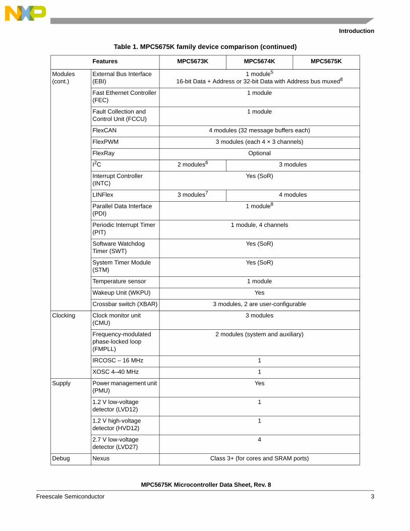
1.3 Device comparisonTable 1. MPC5675K family device comparison
Features MPC5673K MPC5674K MPC5675K
CPU Type 2 × e200z7d (SoR1) in lock-step or decoupled operation
Architecture Harvard
Execution speed 0–150 MHz (+2% FM) 0–180 MHz (+2% FM) 0–180 MHz (+2% FM)
Nominal platform frequency (in 1:1, 1:2, and 1:3 modes)
0–75 MHz (+2% FM) 0–90 MHz (+2% FM) 0–90 MHz (+2% FM)
MMU 64 entries (SoR)
Instruction set PPC Yes
Instruction set VLE Yes
Instruction cache 16 KB, 4-way with EDC (SoR)
Data cache 16 KB, 4-way with Parity (SoR)
MPU Yes (SoR)
Buses Core bus 32-bit address, 64-bit data
Internal periphery bus 32-bit address, 32-bit data
XBAR Master slave ports Yes (SoR)
Memory Static RAM (SRAM) 256 KB (ECC) 384 KB (ECC) 512 KB (ECC)
Code flash memory 1 MB2 (ECC) 1.5 MB2 (ECC) 2 MB2 (ECC)
Data flash memory 64 KB2 (ECC)
Modules
Analog-to-Digital Converter (ADC)
257 pin pkg: 4 × 12 bit (22 external channels)473 pin pkg: 4 × 12 bit (up to 34 external channels)
CRC unit 2 (3 contexts each)
Cross Triggering Unit (CTU)
2 modules
Deserial Serial Peripheral Interface (DSPI)
2 modules (3 chip selects)3
3 modules4
Digital I/Os 16
DRAM Controller (DRAMC)
No Yes5
Enhanced Direct Memory Access (eDMA)
2 modules, 32 channels each
eTimer 3 modules, 6 channels each
Introduction
MPC5675K Microcontroller Data Sheet, Rev. 8
Freescale Semiconductor 3
Modules (cont.)
External Bus Interface (EBI)
1 module5 16-bit Data + Address or 32-bit Data with Address bus muxed8
Fast Ethernet Controller (FEC)
1 module
Fault Collection and Control Unit (FCCU)
1 module
FlexCAN 4 modules (32 message buffers each)
FlexPWM 3 modules (each 4 × 3 channels)
FlexRay Optional
I2C 2 modules6 3 modules
Interrupt Controller (INTC)
Yes (SoR)
LINFlex 3 modules7 4 modules
Parallel Data Interface (PDI)
1 module8
Periodic Interrupt Timer (PIT)
1 module, 4 channels
Software Watchdog Timer (SWT)
Yes (SoR)
System Timer Module (STM)
Yes (SoR)
Temperature sensor 1 module
Wakeup Unit (WKPU) Yes
Crossbar switch (XBAR) 3 modules, 2 are user-configurable
Clocking Clock monitor unit (CMU)
3 modules
Frequency-modulated phase-locked loop (FMPLL)
2 modules (system and auxiliary)
IRCOSC – 16 MHz 1
XOSC 4–40 MHz 1
Supply Power management unit (PMU)
Yes
1.2 V low-voltage detector (LVD12)
1
1.2 V high-voltage detector (HVD12)
1
2.7 V low-voltage detector (LVD27)
4
Debug Nexus Class 3+ (for cores and SRAM ports)
Table 1. MPC5675K family device comparison (continued)
Features MPC5673K MPC5674K MPC5675K

MPC5675K Microcontroller Data Sheet, Rev. 8
Introduction
Freescale Semiconductor4
Packages MAPBGA 257 pins473 pins
Temperature Ambient See the TA recommended operating condition in the device data sheet
1 Sphere of Replication. 2 Does not include Test or Shadow Flash memory space. 3 DSPI_0 and DSPI_1.4 DSPI_0 has 8 chip selects; DSPI_1 and DSPI_2 have 4 chip selects each.5 Available only on 473-pin package.6 Any two of the three I2C can be chosen.7 LinFlex_0, LinFlex_1, and LinFlex_2.8 DDR available only on 473 package. Other modules available as follows:
EBI or DDR on 473 packageEBI + PDI on 473 packageDDR + PDI on 473 packagePDI only on 257 package
Table 1. MPC5675K family device comparison (continued)
Features MPC5673K MPC5674K MPC5675K

Introduction
MPC5675K Microcontroller Data Sheet, Rev. 8
Freescale Semiconductor 5
1.4 Block diagramFigure 1 shows a top-level block diagram of the MPC5675K device.
Figure 1. MPC5675K block diagram
DMA_1
ADC – Analog-to-digital converterBAM – Boot assist moduleCMU – Clock monitoring unitCRC – Cyclic redundancy check unitCTU – Cross triggering unitDSPI – Deserial serial peripheral interfaceEBI – External bus interfaceECC – Error correction codeECSM – Error correction status moduleeDMA – Enhanced direct memory access controllerFCCU – Fault collection and control unit FEC – Fast Ethernet controllerFlexCAN – Controller area network controller FlexPWM – Pulse width modulator module FMPLL – Frequency-modulated phase-locked loopI2C – Inter-integrated circuit controllerINTC – Interrupt controller
IRCOSC – Internal RC oscillatorJTAG – Joint Test Action Group interfaceMC – Mode entry, clock, reset, and power modulesmDDR – Mobile double data rate dynamic RAMPBRIDGE – Peripheral bridgePDI – Parallel data interfacePIT – Periodic interrupt timerPMC – Power management controllerRC – Redundancy checkerRTC – Real time clockSEMA4 – Semaphore unitSIUL – System integration unit LiteSSCM – System status and configuration moduleSTM – System timer moduleSWT – Software watchdog timerTSENS – Temperature sensor XOSC – Crystal oscillator
ECSM_0STM
INTC
Crossbar switch (XBAR_2)
Crossbar switch (XBAR_1)Memory protection unit
PBRIDGE
Debug
l
PBRIDGE
SIU
L
MC
Wak
eUp
AD
C
AD
C
XO
SC
BA
M
SS
CM
Se
con
dar
y P
LL
FM
PLL
IRC
OS
C
CM
U
CM
UC
TU
PIT
FC
CU
Fle
xPW
M
Fle
xPW
M
eTim
er
eTim
er
eTim
er
Fle
xCA
N
Fle
xCA
N
LIN
Fle
x
LIN
Fle
x
DS
PI
DS
PI
DS
PI
CR
C
CM
U
SEMA4
TS
EN
S
PDI
AD
C
AD
C
CT
U
Fle
xPW
M
LIN
Fle
x
LIN
Fle
x
Fle
xCA
N
Fle
xCA
N
DDR Controller
I2C
I2C
I2C
CR
C
DMA_0 Ethernet
PFLASHC PFLASHC
SRAM with ECC LogicSRAM with ECC Logic
PBRIDGE
SWT_0
Crossbar switch (XBAR_0)Memory protection unit
PMC
Redundancy Checker[6]
Redundancy Checker[3]
Redundancy Checker[4]
Redundancy Checker[2]
Redundancy Checker[5]
NexusJTAG
Interface
ECSM_1STM
INTCSEMA4
SWT_1
PMC
External Bus
2MB Flash with ECC Logic
D-CACHE
e200z7dCore_1
I-CACHE
VLE
SPE2
MMU
D-CACHE
e200z7dCore_0
I-CACHE
VLE
SPE2
MMU
Redundancy Checker[7]
Redundancy Checker[0]

MPC5675K Microcontroller Data Sheet, Rev. 8
Introduction
Freescale Semiconductor6
1.5 Feature list• High-performance e200z7d dual core
— 32-bit Power Architecture technology CPU
— Up to 180 MHz core frequency
— Dual-issue core
— Variable length encoding (VLE)
— Memory management unit (MMU) with 64 entries
— 16 KB instruction cache and 16 KB data cache
• Memory available
— Up to 2 MB code flash memory with ECC
— 64 KB data flash memory with ECC
— Up to 512 KB on-chip SRAM with ECC
• SIL3/ASILD innovative safety concept: LockStep mode and fail-safe protection
— Sphere of replication (SoR) for key components
— Redundancy checking units on outputs of the SoR connected to FCCU
— Fault collection and control unit (FCCU)
— Boot-time built-in self-test for memory (MBIST) and logic (LBIST) triggered by hardware
— Boot-time built-in self-test for ADC and flash memory
— Replicated safety-enhanced watchdog timer
— Silicon substrate (die) temperature sensor
— Non-maskable interrupt (NMI)
— 16-region memory protection unit (MPU)
— Clock monitoring units (CMU)
— Power management unit (PMU)
— Cyclic redundancy check (CRC) units
• Decoupled Parallel mode for high-performance use of replicated cores
• Nexus Class 3+ interface
• Interrupts
— Replicated 16-priority interrupt controller
• GPIOs individually programmable as input, output, or special function
• 3 general-purpose eTimer units (6 channels each)
• 3 FlexPWM units with four 16-bit channels per module
• Communications interfaces
— 4 LINFlex modules
— 3 DSPI modules with automatic chip select generation
— 4 FlexCAN interfaces (2.0B Active) with 32 message objects
— FlexRay module (V2.1) with dual channel, up to 128 message objects and up to 10 Mbit/s
— Fast Ethernet Controller (FEC)
— 3 I2C modules
• Four 12-bit analog-to-digital converters (ADCs)
— 22 input channels
— Programmable cross triggering unit (CTU) to synchronize ADC conversion with timer and PWM
• External bus interface
• 16-bit external DDR memory controller
• Parallel digital interface (PDI)

Introduction
MPC5675K Microcontroller Data Sheet, Rev. 8
Freescale Semiconductor 7
• On-chip CAN/UART bootstrap loader
• Capable of operating on a single 3.3 V voltage supply
— 3.3 V-only modules: I/O, oscillators, flash memory
— 3.3 V or 5 V modules: ADCs, supply to internal VREG
— 1.8–3.3 V supply range: DRAM/PDI
• Operating junction temperature range –40 to 150 °C
1.6 Feature details
1.6.1 High-performance e200z7d core processor• Dual 32-bit Power Architecture processor core
• Loose or tight core coupling
• Freescale Variable Length Encoding (VLE) enhancements for code size footprint reduction
• Thirty-two 64-bit general-purpose registers (GPRs)
• Memory management unit (MMU) with 64-entry fully-associative translation look-aside buffer (TLB)
• Branch processing unit
• Fully pipelined load/store unit
• 16 KB Instruction and 16 KB Data caches per core with line locking
— Four way set associative
— Two 32-bit fetches per clock
— Eight-entry store buffer
— Way locking
— Supports tag and data cache parity
— Supports EDC for instruction cache
• Vectored interrupt support
• Signal processing engine 2 (SPE2) auxiliary processing unit (APU) operating on 64-bit general purpose registers
• Floating point
— IEEE 754 compatible with software wrapper
— Single precision in hardware; double precision with software library
— Conversion instructions between single precision floating point and fixed point
• Long cycle time instructions (except for guarded loads) do not increase interrupt latency in the MPC5675K
• To reduce latency, long cycle time instructions are aborted upon interrupt requests
• Extensive system development support through Nexus debug module
1.6.2 Crossbar Switch (XBAR)• 32-bit address bus, 64-bit data bus
• Simultaneous accesses from different masters to different slaves (there is no clock penalty when a parked master accesses a slave)
1.6.3 Memory Protection Unit (MPU)Each master (eDMA, FlexRay, CPU) can be assigned different access rights to each region.
MPC5675K Microcontroller Data Sheet, Rev. 8
Introduction
Freescale Semiconductor8
• 16-region MPU with concurrent checks against each master access
• 32-byte granularity for protected address region
1.6.4 Enhanced Direct Memory Access (eDMA) controller• 32 channels support independent 8-, 16-, 32-bit single value or block transfers
• Supports variable-sized queues and circular queues
• Source and destination address registers are independently configured to post-increment or remain constant
• Each transfer is initiated by a peripheral, CPU, or eDMA channel request
• Each eDMA channel can optionally send an interrupt request to the CPU on completion of a single value or block transfer
1.6.5 Interrupt Controller (INTC)• 208 peripheral interrupt requests
• 8 software settable sources
• Unique 9-bit vector per interrupt source
• 16 priority levels with fixed hardware arbitration within priority levels for each interrupt source
• Priority elevation for shared resources
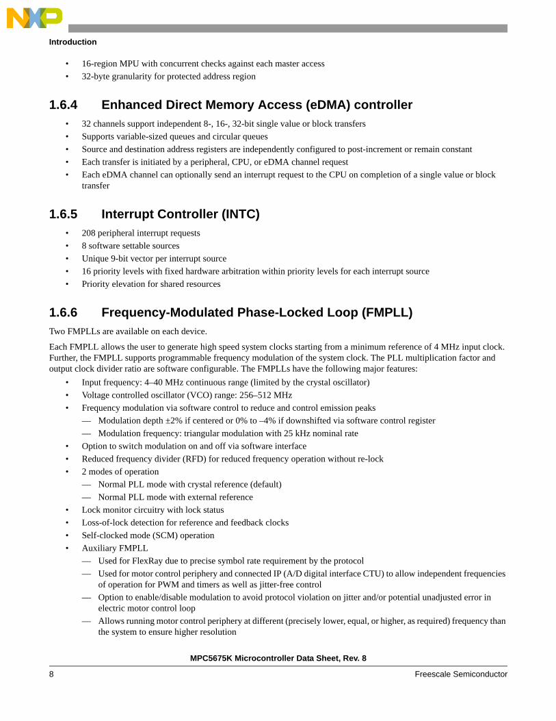
1.6.6 Frequency-Modulated Phase-Locked Loop (FMPLL)Two FMPLLs are available on each device.
Each FMPLL allows the user to generate high speed system clocks starting from a minimum reference of 4 MHz input clock. Further, the FMPLL supports programmable frequency modulation of the system clock. The PLL multiplication factor and output clock divider ratio are software configurable. The FMPLLs have the following major features:
• Input frequency: 4–40 MHz continuous range (limited by the crystal oscillator)
• Voltage controlled oscillator (VCO) range: 256–512 MHz
• Frequency modulation via software control to reduce and control emission peaks
— Modulation depth ±2% if centered or 0% to –4% if downshifted via software control register
— Modulation frequency: triangular modulation with 25 kHz nominal rate
• Option to switch modulation on and off via software interface
• Reduced frequency divider (RFD) for reduced frequency operation without re-lock
• 2 modes of operation
— Normal PLL mode with crystal reference (default)
— Normal PLL mode with external reference
• Lock monitor circuitry with lock status
• Loss-of-lock detection for reference and feedback clocks
• Self-clocked mode (SCM) operation
• Auxiliary FMPLL
— Used for FlexRay due to precise symbol rate requirement by the protocol
— Used for motor control periphery and connected IP (A/D digital interface CTU) to allow independent frequencies of operation for PWM and timers as well as jitter-free control
— Option to enable/disable modulation to avoid protocol violation on jitter and/or potential unadjusted error in electric motor control loop
— Allows running motor control periphery at different (precisely lower, equal, or higher, as required) frequency than the system to ensure higher resolution

Introduction
MPC5675K Microcontroller Data Sheet, Rev. 8
Freescale Semiconductor 9
1.6.7 External Bus Interface (EBI)• Available on 473-pin devices
• Data and address options:
— 16-bit data and address (non-muxed)
— 32-bit data and address (bus-muxed)
• MPC5561 324 BGA compatibility mode: 16-bit data bus, 24-bit address bus is default ADDR[8:31], but configurable to 26-bit address bus
• Memory controller with support for various memory types
— Non-burst and burst mode SDR flash and SRAM
— Asynchronous/legacy flash and SRAM
• Configurable bus speed modes
• Support for 2 MB address space
• Chip select and write/byte enable options as presented in the pin-muxing table in the “Signal Description” chapter of the MPC5675K reference manual
• Configurable wait states (via chip selects)
• Optional automatic CLKOUT gating to save power and reduce EMI
1.6.8 On-chip flash memory• Up to 2 MB code flash memory with ECC
• 64 KB data flash memory with ECC
• Censorship protection scheme to prevent flash content visibility
• Multiple block sizes to support features such as boot block, operating system block, and EEPROM emulation
• Read-while-write with multiple partitions
• Parallel programming mode to support rapid end-of-line programming
• Hardware programming state machine
1.6.9 Cache memory• Harvard architecture cache
• 16 KB instruction / 16 KB data
• Four-way set-associative Harvard (instruction and data) 256-bit long cache
— Two 32-bit fetches per clock
— Eight-entry store buffer
— Way locking
— Supports tag and data cache parity
— Supports EDC for instruction cache
1.6.10 On-chip internal static RAM (SRAM)• Up to 512 KB general-purpose SRAM
• ECC performs single-bit correction, double-bit error detection
— Address included in ECC checkbase
MPC5675K Microcontroller Data Sheet, Rev. 8
Introduction
Freescale Semiconductor10
1.6.11 DRAM controllerThe DRAM controller (available only on 473-pin devices) is a multi-port controller that monitors incoming requests on the three AHB slave ports and decides (at each rising clock edge) what command needs to be sent to the external DRAM.
The DRAM controller on this device supports the following types of memories:
• Mobile DDR (mDDR)
• DDR 1
• DDR 2 (optional)
• SDR
The controller has the following features:
• Optimized timing for 32-byte bursts and single read accesses on the AHB interface
• Optimized timing for 8-byte and 16-byte bursts on the DRAMC interface
• Supports priority elevation on the slave ports for single accesses
• 16-bit wide DRAM interface
• One chip select (CS)
• mDDR memory controller
— 16-bit external interface
— Address range up to 8 MB
1.6.12 Boot Assist Module (BAM)• Enables booting via serial mode (FlexCAN, LINFlex)
• Handles static mode in case of an erroneous boot procedure
• Implemented in 8 KB ROM
• Supports Lock Step Mode (LSM) and Decoupled Parallel Mode (DPM)
1.6.13 Parallel Data Interface (PDI)• Support for external ADC and CMOS image sensors
• Parallel interface operation up to MCU system bus frequency
• Selectable data capture from rising or falling edge
• Receive FIFO with adjustable trigger thresholds
• Data width for 8, 10, 12, 14, and 16 bits
• Data Packing Unit to pack input data on 64-bit words — data packed on 8- or 16- bit boundary, depending on input data width
• Binary increasing channel select that allows as many as eight channels to be selected
• Frame synchronization through Vsync, Hsync, PIXCLK
1.6.14 Deserial Serial Peripheral Interface (DSPI) modules• Three serial peripheral interfaces
— Full duplex communication ports with interrupt and eDMA request support
— Support for all functional modes from QSPI submodule of QSMCM (MPC5xx family)
— Support for queues in RAM
— Six chip selects, expandable to 64 with external demultiplexers
— Programmable frame size, baud rate, clock delay, and clock phase on a per-frame basis
Introduction
MPC5675K Microcontroller Data Sheet, Rev. 8
Freescale Semiconductor 11
— Modified SPI mode for interfacing to peripherals with longer setup time requirements
• Support for up to 60 Mbit/s in slave only Rx mode
1.6.15 Serial Communication Interface Module (LINFlex)The LINFlex on this device features the following:
• Supports LIN Master mode, LIN Slave mode, and UART mode
• LIN state machine compliant to LIN1.3, 2.0, and 2.1 specifications
• Manages LIN frame transmission and reception without CPU intervention
• LIN features
— Autonomous LIN frame handling
— Message buffer to store as many as 8 data bytes
— Supports messages as long as 64 bytes
— Detection and flagging of LIN errors (Sync field, delimiter, ID parity, bit framing, checksum and timeout errors)
— Classic or extended checksum calculation
— Configurable break duration of up to 36-bit times
— Programmable baud rate prescalers (13-bit mantissa, 4-bit fractional)
— Diagnostic features (loop back, LIN bus stuck dominant detection)
— Interrupt-driven operation with 16 interrupt sources
• LIN slave mode features
— Autonomous LIN header handling
— Autonomous LIN response handling
• UART mode
— Full-duplex operation
— Standard non return-to-zero (NRZ) mark/space format
— Data buffers with 4-byte receive, 4-byte transmit
— Configurable word length (8-bit, 9-bit, or 16-bit words)
— Configurable parity scheme: none, odd, even, always 0
— Speed as fast as 2 Mbit/s
— Error detection and flagging (parity, noise, and framing errors)
— Interrupt-driven operation with four interrupt sources
— Separate transmitter and receiver CPU interrupt sources
— 16-bit programmable baud-rate modulus counter and 16-bit fractional
— Two receiver wake-up methods
• Support for DMA-enabled transfers
1.6.16 FlexCAN• Thirty-two message buffers each
• Full implementation of the CAN protocol specification, Version 2.0B
• Programmable acceptance filters
• Individual Rx filtering per message buffer
• Short latency time for high priority transmit messages
• Arbitration scheme according to message ID or message buffer number
• Listen-only mode capabilities
• Programmable clock source: system clock or oscillator clock
MPC5675K Microcontroller Data Sheet, Rev. 8
Introduction
Freescale Semiconductor12
• Reception queue possible by setting more than one Rx message buffer with the same ID
• Backwards compatible with previous FlexCAN modules
• Safety CAN features on 1 CAN module as implemented on MPC5604P
1.6.17 Dual-channel FlexRay controller• Full implementation of FlexRay Protocol Specification 2.1
• Sixty-four configurable message buffers can be handled
• Message buffers configurable as Tx, Rx, or RxFIFO
• Message buffer size configurable
• Message filtering for all message buffers based on FrameID, cycle count, and message ID
• Programmable acceptance filters for RxFIFO message buffers
• Dual channel, each at up to 10 Mbit/s data rate
1.6.18 Periodic Interrupt Timer (PIT)The PIT module implements the features below:
• Four general-purpose interrupt timers
• 32-bit counter resolution
• Clocked by system clock frequency
• 32-bit counter for real time interrupt, clocked from main external oscillator
• Can be used for software tick or DMA trigger operation
1.6.19 System Timer Module (STM)The STM implements the features below:
• Replicated periphery to provide safety measures respective to high safety integrity levels (for example, SIL 3, ASIL D)
• Up-counter with four output compare registers
• OS task protection and hardware tick implementation as per current state-of-the-art AUTOSAR requirement
1.6.20 Motor control (MOTC) peripheralsThe peripherals in this section can be used for general-purpose applications, but are specifically designed for motor control (MOTC) applications.
1.6.20.1 FlexPWM
The pulse width modulator module (FlexPWM) contains three PWM channels, each of which is configured to control a single half-bridge power stage. There may also be one or more fault channels.
This PWM is capable of controlling most motor types: AC induction motors (ACIM), permanent magnet AC motors (PMAC), both brushless (BLDC) and brush DC motors (BDC), switched (SRM) and variable reluctance motors (VRM), and stepper motors.
A FlexPWM module implements the following features:
• 16 bits of resolution for center, edge aligned, and asymmetrical PWMs
• Maximum operating frequency lower than or equal to platform frequency
• Clock source not modulated and independent from system clock (generated via auxiliary PLL)
• Fine granularity control for enhanced resolution of the PWM period

Introduction
MPC5675K Microcontroller Data Sheet, Rev. 8
Freescale Semiconductor 13
• PWM outputs can operate as complementary pairs or independent channels
• Ability to accept signed numbers for PWM generation
• Independent control of both edges of each PWM output
• Synchronization to external hardware or other PWM is supported
• Double-buffered PWM registers
— Integral reload rates from 1 to 16
— Half-cycle reload capability
• Multiple ADC trigger events can be generated per PWM cycle via hardware
• Fault inputs can be assigned to control multiple PWM outputs
• Programmable filters for fault inputs
• Independently programmable PWM output polarity
• Independent top and bottom deadtime insertion
• Each complementary pair can operate with its own PWM frequency and deadtime values
• Individual software control for each PWM output
• All outputs can be forced to a value simultaneously
• PWMX pin can optionally output a third signal from each channel
• Channels not used for PWM generation can be used for:
— buffered output compare functions
— input capture functions
• Enhanced dual-edge capture functionality
• Option to supply the source for each complementary PWM signal pair from any of the following:
— External digital pin
— Internal timer channel
— External ADC input, taking into account values set in ADC high and low limit registers
• Supports safety measures using DMA
1.6.20.2 Cross Triggering Unit (CTU)
The CTU provides automatic generation of ADC conversion requests on user-selected conditions without CPU load during the PWM period and with minimized CPU load for dynamic configuration.
The CTU implements the following features:
• Cross triggering between ADC, FlexPWM, eTimer, and external pins
• Double-buffered trigger generation unit with as many as eight independent triggers generated from external triggers
• Maximum operating frequency lower than or equal to platform
• Trigger generation unit configurable in sequential mode or in triggered mode
• Trigger delay unit to compensate the delay of external low-pass filter
• Double-buffered global trigger unit allowing eTimer synchronization and/or ADC command generation
• Double-buffered ADC command list pointers to minimize ADC trigger unit update
• Double-buffered ADC conversion command list with as many as twenty-four ADC commands
• Each trigger has the capability to generate consecutive commands
• ADC conversion command allows controlling ADC channel from each ADC, single or synchronous sampling, independent result queue selection
• Supports safety measures using DMA

MPC5675K Microcontroller Data Sheet, Rev. 8
Introduction
Freescale Semiconductor14
1.6.20.3 Analog-To-Digital Converter (ADC)
• Four independent ADCs with 12-bit A/D resolution
• Common mode conversion range of 0–5 V or 0–3.3 V
• Twenty-two single-ended input channels
• Supports eight FIFO queues with fixed priority
• Queue modes with priority-based preemption; initiated by software command, internal, or external triggers
• DMA and interrupt request support
1.6.20.4 eTimer module
Three 16-bit general purpose up/down timer/counters per module are implemented with the following features:
• Ability to operate up to platform frequency
• Individual channel capability
— Input capture trigger
— Output compare
— Double buffer (to capture rising edge and falling edge)
— Separate prescaler for each counter
— Selectable clock source
— 0–100% pulse measurement
— Rotation direction flag (quad decoder mode)
• Maximum count rate
— Equals peripheral clock/2 for external event counting
— Equals peripheral clock for internal clock counting
• Cascadeable counters
• Programmable count modulo
• Quadrature decode capabilities
• Counters can share available input pins
• Count once or repeatedly
• Preloadable counters
• Pins available as GPIO when timer functionality is not in use
• DMA support
1.6.21 Redundancy Control and Checker Unit (RCCU)The RCCU checks all outputs of the sphere of replication (addresses, data, control signals). It has the following features:
• Duplicated module to enable high diagnostic coverage (check of checker)
• Replicated IP to be used as checkers on the PBRIDGE output, Flash Controller output, SRAM output, DMA Channel Mux inputs
1.6.22 Software Watchdog Timer (SWT)This module implements the features below:
• Replicated periphery to provide safety measures respective to high safety integrity levels (for example, SIL 3, ASIL D)
• Fault-tolerant output
• Safe internal RC oscillator as reference clock
• Windowed watchdog

Introduction
MPC5675K Microcontroller Data Sheet, Rev. 8
Freescale Semiconductor 15
• Program flow control monitor with 16-bit pseudorandom key generation
• Provides measures to target high safety integrity levels (for example, SIL 3, ASIL D)
1.6.23 Fault Collection and Control Unit (FCCU)The FCCU module has the following features:
• Redundant collection of hardware checker results
• Redundant collection of error information and latch of faults from critical modules on the device
• Collection of test results
• Configurable and graded fault control
— Internal reactions (no internal reaction, NMI, reset, or safe mode)
— External reaction (failure is reported to the outside world via configurable output pins)
1.6.24 System Integration Unit Lite (SIUL)The SIUL controls MCU reset configuration, pad configuration, external interrupt, general purpose I/O (GPIO), internal peripheral multiplexing, and the system reset operation. The reset configuration block contains the external pin boot configuration logic. The pad configuration block controls the static electrical characteristics of I/O pins. The GPIO block provides uniform and discrete input/output control of the I/O pins of the MCU.
The SIUL provides the following features:
• Centralized pad control on a per-pin basis
— Pin function selection
— Configurable weak pullup/pulldown
— Configurable slew rate control (slow/medium/fast)
— Hysteresis on GPIO pins
— Configurable automatic safe mode pad control
• Input filtering for external interrupts
1.6.25 Cyclic Redundancy Checker (CRC) unitThe CRC module is a configurable multiple data flow unit to compute CRC signatures on data written to an input register.
The CRC unit has the following features:
• Three sets of registers to allow three concurrent contexts with possibly different CRC computations, each with a selectable polynomial and seed
• Computes 16- or 32-bit wide CRC on the fly (single-cycle computation) and stores the result in an internal register
• Implements the following standard CRC polynomials:
— x16 + x12 + x5 + 1 [16-bit CRC-CCITT]
— x32 + x26 + x23 + x22 + x16 + x12 + x11 + x10 + x8 + x7 + x5 + x4 + x2 + x + 1 [32-bit CRC-ethernet(32)]
• Key engine to be coupled with communication periphery where CRC application is added to support implementation of safe communication protocol
• Offloads the core from cycle-consuming CRC and helps in checking the configuration signature for safe start-up or periodic procedures
• Connected as a peripheral on the internal peripheral bus
• Provides DMA support

MPC5675K Microcontroller Data Sheet, Rev. 8
Introduction
Freescale Semiconductor16
1.6.26 Non-Maskable Interrupt (NMI)The non-maskable interrupt with de-glitching filter is available to support high priority core exceptions.
1.6.27 System Status and Configuration Module (SSCM)The SSCM on the MPC5675K features the following:
• System configuration and status
• Debug port status and debug port enable
• Multiple boot code starting locations out of reset through implementation of search for valid reset configuration halfword
• Sets up the MMU to allow user boot code to execute as either Classic Power Architecture Book E code (default) or as Freescale VLE code out of flash
• Supports serial bootloading of either Classic Power Architecture Book E code (default) or Freescale VLE code
• Detection of user boot code
• Automatic switch to serial boot mode if internal flash is blank or invalid
1.6.28 Nexus Development Interface (NDI)• Per IEEE-ISTO 5001-2008
• Real-time development support for Power Architecture core through Nexus class 3 (some class 4 support)
• Nexus support to snoop system SRAM traffic
• Data trace of FlexRay accesses
• Read and write access
• Configured via the IEEE 1149.1 (JTAG) port
• High bandwidth mode for fast message transmission
• Reduced bandwidth mode for reduced pin usage
1.6.29 IEEE 1149.1 JTAG Controller (JTAGC)• IEEE 1149.1-2001 Test Access Port (TAP) interface
• JCOMP input that provides the ability to share the TAP —selectable modes of operation include JTAGC/debug or normal system operation
• 5-bit instruction register that supports IEEE 1149.1-2001 defined instructions
• 5-bit instruction register that supports additional public instructions
• Three test data registers:
— Bypass register
— Boundary scan register
— Device identification register
• TAP controller state machine that controls the operation of the data registers, instruction register, and associated circuitry
Package pinouts and signal descriptions
MPC5675K Microcontroller Data Sheet, Rev. 8
Freescale Semiconductor 17
2 Package pinouts and signal descriptions
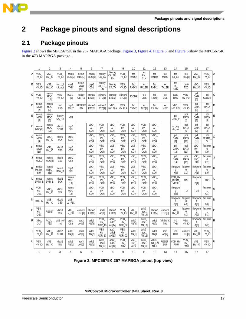
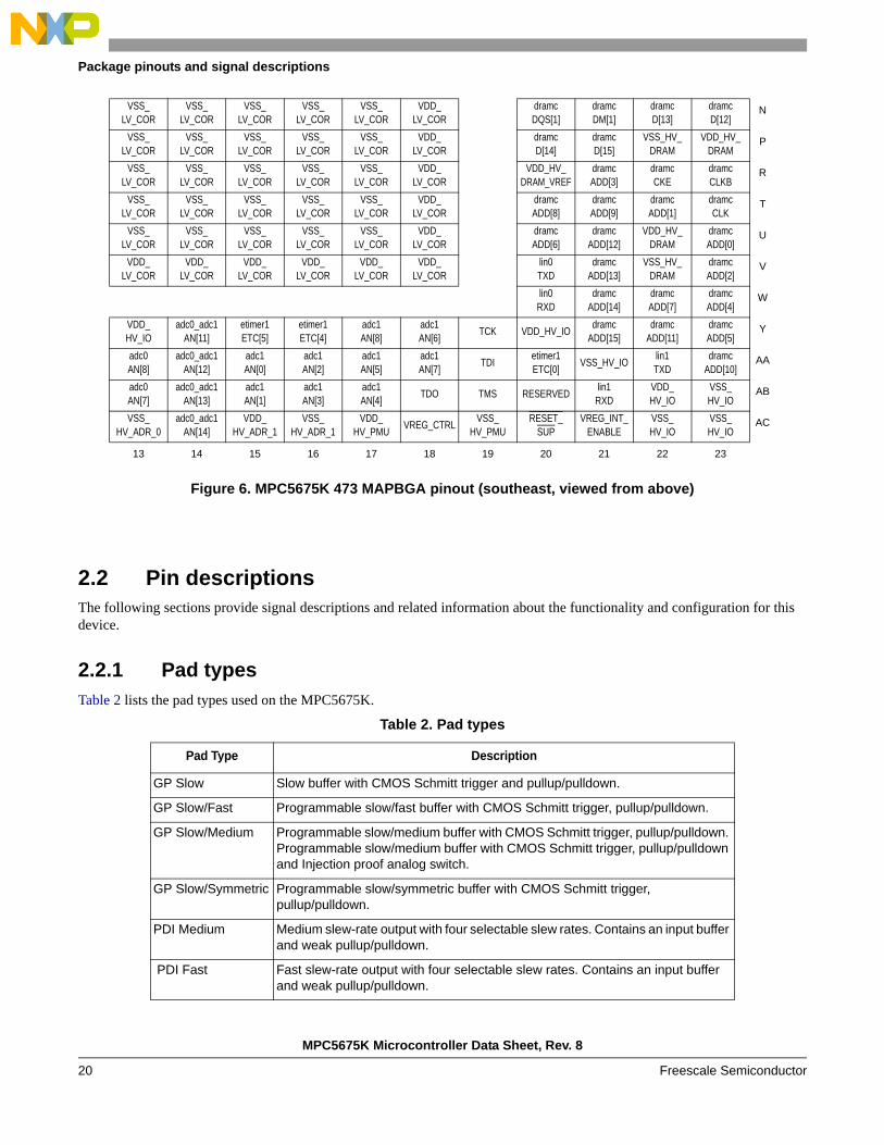
2.1 Package pinoutsFigure 2 shows the MPC5675K in the 257 MAPBGA package. Figure 3, Figure 4, Figure 5, and Figure 6 show the MPC5675K in the 473 MAPBGA package.
Figure 2. MPC5675K 257 MAPBGA pinout (top view)
1 2 3 4 5 6 7 8 9 10 11 12 13 14 15 16 17
A VSS_HV_IO
VSS_HV_IO
VDD_HV_IO
nexusMDO[5]
nexusMDO[7]
nexusMDO[9]
flexrayCB_TX
flexrayCA_TR_
EN
VDD_HV_IO
fecRXD[2]
fecRX_CLK
fecRXD[0]
fecMDIO
fecTX_EN
fecTXD[3]
VSS_HV_IO
VSS_HV_IO
A
B VSS_HV_IO
VSS_HV_IO
mc_cglclk_out
can1TXD
nexusMDO[14]
dspi2CS1
flexrayCB_TR_
EN
flexrayCA_TX
VSS_HV_IO
fecRXD[3]
fecRX_ER
fecRXD[1]
fecTX_ER
fecTX_CLK
can0TXD
VDD_HV_IO
VSS_HV_IO
B
C VDD_HV_IO
nexusMDO[15]
VSS_HV_IO
FCCU_F[1]
flexrayCB_RX
etimer0ETC[0]
etimer0ETC[1]
etimer0ETC[2]
etimer0ETC[3] JCOMP fec
CRSfec
TXD[0]fec
COLcan0RXD
VSS_HV_PDI
pdiDATA
[5]
pdiCLOCK
C
D nexusMDO
[2]
nexusMDO
[3]
can1RXD
dspi0SOUT
RESERVED
etimer0ETC[5]
etimer0ETC[4]
VDD_HV_FLA
VSS_HV_FLA
fecTXD[2]
fecTXD[1]
fecRX_DV
fecMDC
VDD_HV_PDI
VSS_HV_IO
pdiDATA
[0]
pdiDATA
[1]
D
E nexusMDO
[0]
nexusMDO
[1]
flexrayCA_RX NMI pdi
LINE_V
pdiDATA
[2]
pdiDATA
[3]
pdiDATA
[4]
E
F nexusMDO[6]
nexusMDO[11]
dspi1SOUT
dspi1SIN
VDD_LV_COR
VDD_LV_COR
VDD_LV_COR
VDD_LV_COR
VDD_LV_COR
VDD_LV_COR
VDD_LV_COR
mc_cglclk_out
pdiDATA
[6]
pdiDATA
[7]
pdiDATA
[8]
F
G nexusMDO
[4]
VDD_HV_IO
dspi0SCK
dspi1SCK
VDD_LV_COR
VSS_LV_COR
VSS_LV_COR
VSS_LV_COR
VSS_LV_COR
VSS_LV_COR
VDD_LV_COR
pdiDATA
[9]
pdiDATA[10]
pdiDATA[11]
pdiFRAME_
V
G
H nexusMDO[10]
VSS_HV_IO
dspi0CS0
dspi1CS0
VDD_LV_COR
VSS_LV_COR
VSS_LV_COR
VSS_LV_COR
VSS_LV_COR
VSS_LV_COR
VDD_LV_COR
pdiDATA[12]
pdiDATA[13]
VDD_HV_PDI
flexpwm0
X[0]
H
J nexusMCKO
nexusMDO[8]
dspi2CS0
dspi2CS2
VDD_LV_COR
VSS_LV_COR
VSS_LV_COR
VSS_LV_COR
VSS_LV_COR
VSS_LV_COR
VDD_LV_COR
pdiDATA[14]
pdiDATA[15]
VSS_HV_PDI
flexpwm0
X[1]
J
K nexusMSEO_
B[0]
nexusMSEO_
B[1]
nexusRDY_B
dspi0SIN
VDD_LV_COR
VSS_LV_COR
VSS_LV_COR
VSS_LV_COR
VSS_LV_COR
VSS_LV_COR
VDD_LV_COR
flexpwm0
X[2]
flexpwm0
X[3]
flexpwm0
A[1]
flexpwm0
B[0]
K
L nexusEVTO_B
nexusEVTI_B
dspi2SCK
nexusMDO[13]
VDD_LV_COR
VSS_LV_COR
VSS_LV_COR
VSS_LV_COR
VSS_LV_COR
VSS_LV_COR
VDD_LV_COR
VDD_HV_DRAM_
VREFTCK
flexpwm0
B[1]TDO
L
M VDD_HV_OSC
VDD_HV_IO
dspi1CS2
nexusMDO[12]
VDD_LV_COR
VDD_LV_COR
VDD_LV_COR
VDD_LV_COR
VDD_LV_COR
VDD_LV_COR
VDD_LV_COR
flexpwm0
B[2]TDI TMS
flexpwm1
A[1]
M
NXTALIN VSS_
HV_IOdspi0CS3
VSS_LV_PLL
flexpwm0
B[3]
flexpwm0
A[2]
flexpwm1
A[0]
flexpwm1
B[0]
N
P VSS_HV_OSC
RESET dspi0CS2
VDD_LV_PLL
etimer1ETC[1]
etimer1ETC[2]
adc0AN[0]
etimer1ETC[3]
VSS_HV_IO
VDD_HV_IO
adc0_adc1
AN[14]
etimer1ETC[4]
etimer1ETC[5]
VDD_HV_IO
flexpwm0
A[3]
flexpwm0
A[0]
flexpwm1
B[1]
P
R XTALOUT
FCCU_F[0]
VSS_HV_IO
dspi1CS3
adc2AN[0]
adc2AN[3]
VDD_HV_
ADR_13
adc2_adc3
AN[14]
VDD_HV_
ADR_02
adc0AN[2]
adc0_adc1
AN[13]
adc1AN[1]
VREG_CTRL
lin0TXD
VSS_HV_IO
flexpwm1
A[2]
flexpwm1
B[2]
R
T VSS_HV_IO
VDD_HV_IO
dspi2SOUT
adc3AN[0]
adc3AN[3]
adc2AN[2]
VSS_HV_
ADR_13
adc2_adc3
AN[13]
VSS_HV_
ADR_02
adc0AN[1]
adc0_adc1
AN[12]
adc1AN[0]
adc1AN[2]
lin0RXD
etimer1ETC[0]
VDD_HV_IO
VSS_HV_IO
T
U VSS_HV_IO
VSS_HV_IO
dspi2SIN
adc3AN[1]
adc3AN[2]
adc2AN[1]
adc2_adc3
AN[11]
adc2_adc3
AN[12]
VDD_HV_ADV
VSS_HV_ADV
adc0_adc1
AN[11]
VREG_INT_ENABLE
RESET_SUP
VDD_HV_PMU
VSS_HV_PMU
VSS_HV_IO
VSS_HV_IO
U
1 2 3 4 5 6 7 8 9 10 11 12 13 14 15 16 17

MPC5675K Microcontroller Data Sheet, Rev. 8
Package pinouts and signal descriptions
Freescale Semiconductor18
Figure 3. MPC5675K 473 MAPBGA pinout (northwest, viewed from above)
1 2 3 4 5 6 7 8 9 10 11 12
A VSS_HV_IO
VSS_HV_IO
VDD_HV_IO
nexusMDO[5]
nexusMDO[7]
nexusMDO[9]
flexrayCB_TX
flexrayCA_TR_EN
fecRX_DV
fecMDIO
fecTX_CLK
fecTX_EN
B VSS_HV_IO
VSS_HV_IO
mc_cglclk_out
can1TXD
nexusMDO[14]
dspi2CS1
flexrayCB_TR_EN
flexrayCA_TX
fecRXD[3]
fecRX_ER
fecTXD[0]
fecRXD[0]
C VDD_HV_IO
nexusMDO[15]
VSS_HV_IO
FCCU_F[1]
flexrayCB_RX
etimer0ETC[4]
etimer0ETC[1]
etimer0ETC[2]
etimer0ETC[3]
fecTXD[2]
fecTXD[1]
fecCRS
D nexusMDO[1]
nexusMDO[3]
can1RXD
dspi0SOUT
RESERVEDetimer0ETC[5]
etimer0ETC[0]
VDD_HV_IO
VSS_HV_IO
JCOMPVSS_HV_IO
VSS_HV_FLA
E nexusMDO[0]
nexusMDO[2]
flexrayCA_RX
NMI
F nexusMDO[10]
nexusMDO[11]
nexusMDO[6]
nexusMDO[4]
VDD_LV_COR
VDD_LV_COR
VDD_LV_COR
VDD_LV_COR
VDD_LV_COR
VDD_LV_COR
VDD_LV_COR
G nexusMCKO
VDD_HV_IO
nexusMDO[8]
nexusMSEO_B[1]
VDD_LV_COR
VSS_LV_COR
VSS_LV_COR
VSS_LV_COR
VSS_LV_COR
VSS_LV_COR
VSS_LV_COR
H nexusEVTO_B
VSS_HV_IO
nexusMSEO_B[0]
nexusEVTI_B
VDD_LV_COR
VSS_LV_COR
VSS_LV_COR
VSS_LV_COR
VSS_LV_COR
VSS_LV_COR
VSS_LV_COR
J nexusRDY_B
nexusMDO[13]
nexusMDO[12]
dspi1SIN
VDD_LV_COR
VSS_LV_COR
VSS_LV_COR
VSS_LV_COR
VSS_LV_COR
VSS_LV_COR
VSS_LV_COR
K dspi0SCK
dspi1CS0
dspi1SCK
dspi1SOUT
VDD_LV_COR
VSS_LV_COR
VSS_LV_COR
VSS_LV_COR
VSS_LV_COR
VSS_LV_COR
VSS_LV_COR
L dspi0CS0
dspi2CS2
dspi2CS0
VSS_HV_IO
VDD_LV_COR
VSS_LV_COR
VSS_LV_COR
VSS_LV_COR
VSS_LV_COR
VSS_LV_COR
VSS_LV_COR
M flexpwm0X[0]
VDD_HV_IO
dspi0SIN
VDD_HV_IO
VDD_LV_COR
VSS_LV_COR
VSS_LV_COR
VSS_LV_COR
VSS_LV_COR
VSS_LV_COR
VSS_LV_COR

Package pinouts and signal descriptions
MPC5675K Microcontroller Data Sheet, Rev. 8
Freescale Semiconductor 19
Figure 4. MPC5675K 473 MAPBGA pinout (southwest, viewed from above)
Figure 5. MPC5675K 473 MAPBGA pinout (northeast, viewed from above)
N flexpwm0A[0]
VSS_HV_IO
flexpwm0X[1]
flexpwm0B[2]
VDD_LV_COR
VSS_LV_COR
VSS_LV_COR
VSS_LV_COR
VSS_LV_COR
VSS_LV_COR
VSS_LV_COR
P flexpwm0B[0]
flexpwm0B[1]
flexpwm0A[2]
flexpwm0A[3]
VDD_LV_COR
VSS_LV_COR
VSS_LV_COR
VSS_LV_COR
VSS_LV_COR
VSS_LV_COR
VSS_LV_COR
R flexpwm0X[2]
flexpwm0X[3]
flexpwm0A[1]
VSS_HV_IO
VDD_LV_COR
VSS_LV_COR
VSS_LV_COR
VSS_LV_COR
VSS_LV_COR
VSS_LV_COR
VSS_LV_COR
T flexpwm0B[3]
flexpwm1A[0]
flexpwm1A[1]
VDD_HV_IO
VDD_LV_COR
VSS_LV_COR
VSS_LV_COR
VSS_LV_COR
VSS_LV_COR
VSS_LV_COR
VSS_LV_COR
U flexpwm1B[0]
flexpwm1B[1]
flexpwm1A[2]
dspi2SCK
VDD_LV_COR
VSS_LV_COR
VSS_LV_COR
VSS_LV_COR
VSS_LV_COR
VSS_LV_COR
VSS_LV_COR
V VDD_HV_OSC
VDD_HV_IO
flexpwm1B[2]
dspi1CS2
VDD_LV_COR
VDD_LV_COR
VDD_LV_COR
VDD_LV_COR
VDD_LV_COR
VDD_LV_COR
VDD_LV_COR
W XTALINVSS_HV_IO
dspi0CS3
VSS_LV_PLL
Y VSS_HV_OSC
RESET dspi0CS2
VDD_LV_PLL
flexpwm1X[0]
adc3AN[0]
adc2_adc3AN[11]
adc2_adc3AN[14]
etimer1ETC[1]
etimer1ETC[2]
etimer1ETC[3]
VSS_HV_IO
AA XTALOUTFCCU_
F[0]VSS_HV_IO
dspi1CS3
flexpwm1X[1]
adc3AN[1]
adc2_adc3AN[12]
adc2AN[0]
VDD_HV_ADV
VSS_HV_ADV
adc0AN[2]
adc0AN[5]
AB VSS_HV_IO
VDD_HV_IO
dspi2SOUT
flexpwm1X[2]
flexpwm1X[3]
adc3AN[2]
adc2_adc3AN[13]
adc2AN[1]
adc2AN[2]
adc0AN[0]
adc0AN[4]
adc0AN[6]
AC VSS_HV_IO
VSS_HV_IO
dspi2SIN
flexpwm1A[3]
flexpwm1B[3]
adc3AN[3]
VDD_HV_ADR_23
VSS_HV_ADR_23
adc2AN[3]
adc0AN[1]
adc0AN[3]
VDD_HV_ADR_0
1 2 3 4 5 6 7 8 9 10 11 12
13 14 15 16 17 18 19 20 21 22 23
fecTXD[3]
VDD_HV_IO
pdiDATA[3]
pdiDATA[1]
pdiCLOCK
pdiDATA[7]
pdiDATA[10]
pdiDATA[13]
pdiDATA[15]
VSS_HV_IO
VSS_HV_IO
A
fecTX_ER
VSS_HV_IO
pdiDATA[6]
pdiDATA[4]
pdiDATA[0]
pdiLINE_V
pdiDATA[9]
pdiDATA[14]
can0TXD
VDD_HV_IO
VSS_HV_IO
B
fecRX_CLK
fecRXD[1]
fecCOL
pdiDATA[5]
pdiDATA[2]
pdiDATA[8]
pdiDATA[12]
can0RXD
VSS_HV_PDI
siulGPIO[197]
dramcCAS
C
VDD_HV_FLA
fecRXD[2]
fecMDC
VDD_HV_PDI
VSS_HV_PDI
pdiDATA[11]
pdiFRAME_V
VDD_HV_PDI
dramcBA[1]
siulGPIO[195]
dramcBA[0]
D
mc_cglclk_out
siulGPIO[149]
dramcCS0
dramcBA[2]
E
VDD_LV_COR
VDD_LV_COR
VDD_LV_COR
VDD_LV_COR
VDD_LV_COR
VDD_LV_COR
dramcRAS
siulGPIO[194]
siulGPIO[148]
dramcD[5]
F
VSS_LV_COR
VSS_LV_COR
VSS_LV_COR
VSS_LV_COR
VSS_LV_COR
VDD_LV_COR
siulGPIO[196]
dramcDQS[0]
dramcDM[0]
dramcD[7]
G
VSS_LV_COR
VSS_LV_COR
VSS_LV_COR
VSS_LV_COR
VSS_LV_COR
VDD_LV_COR
dramcD[2]
VDD_HV_DRAM_VTT
VDD_HV_DRAM
VSS_HV_DRAM
H
VSS_LV_COR
VSS_LV_COR
VSS_LV_COR
VSS_LV_COR
VSS_LV_COR
VDD_LV_COR
dramcD[0]
dramcD[1]
dramcD[3]
dramcD[6]
J
VSS_LV_COR
VSS_LV_COR
VSS_LV_COR
VSS_LV_COR
VSS_LV_COR
VDD_LV_COR
VSS_HV_IO
dramcD[4]
dramcD[8]
dramcD[9]
K
VSS_LV_COR
VSS_LV_COR
VSS_LV_COR
VSS_LV_COR
VSS_LV_COR
VDD_LV_COR
VDD_HV_IO
VDD_HV_DRAM_VTT
VSS_HV_DRAM
VDD_HV_DRAM
L
VSS_LV_COR
VSS_LV_COR
VSS_LV_COR
VSS_LV_COR
VSS_LV_COR
VDD_LV_COR
dramcODT
dramcWEB
dramcD[11]
dramcD[10]
M
MPC5675K Microcontroller Data Sheet, Rev. 8
Package pinouts and signal descriptions
Freescale Semiconductor20
Figure 6. MPC5675K 473 MAPBGA pinout (southeast, viewed from above)
2.2 Pin descriptionsThe following sections provide signal descriptions and related information about the functionality and configuration for this device.
2.2.1 Pad typesTable 2 lists the pad types used on the MPC5675K.
VSS_LV_COR
VSS_LV_COR
VSS_LV_COR
VSS_LV_COR
VSS_LV_COR
VDD_LV_COR
dramcDQS[1]
dramcDM[1]
dramcD[13]
dramcD[12]
N
VSS_LV_COR
VSS_LV_COR
VSS_LV_COR
VSS_LV_COR
VSS_LV_COR
VDD_LV_COR
dramcD[14]
dramcD[15]
VSS_HV_DRAM
VDD_HV_DRAM
P
VSS_LV_COR
VSS_LV_COR
VSS_LV_COR
VSS_LV_COR
VSS_LV_COR
VDD_LV_COR
VDD_HV_DRAM_VREF
dramcADD[3]
dramcCKE
dramcCLKB
R
VSS_LV_COR
VSS_LV_COR
VSS_LV_COR
VSS_LV_COR
VSS_LV_COR
VDD_LV_COR
dramcADD[8]
dramcADD[9]
dramcADD[1]
dramcCLK
T
VSS_LV_COR
VSS_LV_COR
VSS_LV_COR
VSS_LV_COR
VSS_LV_COR
VDD_LV_COR
dramcADD[6]
dramcADD[12]
VDD_HV_DRAM
dramcADD[0]
U
VDD_LV_COR
VDD_LV_COR
VDD_LV_COR
VDD_LV_COR
VDD_LV_COR
VDD_LV_COR
lin0TXD
dramcADD[13]
VSS_HV_DRAM
dramcADD[2]
V
lin0RXD
dramcADD[14]
dramcADD[7]
dramcADD[4]
W
VDD_HV_IO
adc0_adc1AN[11]
etimer1ETC[5]
etimer1ETC[4]
adc1AN[8]
adc1AN[6]
TCK VDD_HV_IOdramc
ADD[15]dramc
ADD[11]dramcADD[5]
Y
adc0AN[8]
adc0_adc1AN[12]
adc1AN[0]
adc1AN[2]
adc1AN[5]
adc1AN[7]
TDIetimer1ETC[0]
VSS_HV_IOlin1TXD
dramcADD[10]
AA
adc0AN[7]
adc0_adc1AN[13]
adc1AN[1]
adc1AN[3]
adc1AN[4]
TDO TMS RESERVEDlin1
RXDVDD_HV_IO
VSS_HV_IO
AB
VSS_HV_ADR_0
adc0_adc1AN[14]
VDD_HV_ADR_1
VSS_HV_ADR_1
VDD_HV_PMU
VREG_CTRLVSS_
HV_PMURESET_
SUPVREG_INT_
ENABLEVSS_HV_IO
VSS_HV_IO
AC
13 14 15 16 17 18 19 20 21 22 23
Table 2. Pad types
Pad Type Description
GP Slow Slow buffer with CMOS Schmitt trigger and pullup/pulldown.
GP Slow/Fast Programmable slow/fast buffer with CMOS Schmitt trigger, pullup/pulldown.
GP Slow/Medium Programmable slow/medium buffer with CMOS Schmitt trigger, pullup/pulldown. Programmable slow/medium buffer with CMOS Schmitt trigger, pullup/pulldown and Injection proof analog switch.
GP Slow/Symmetric Programmable slow/symmetric buffer with CMOS Schmitt trigger, pullup/pulldown.
PDI Medium Medium slew-rate output with four selectable slew rates. Contains an input buffer and weak pullup/pulldown.
PDI Fast Fast slew-rate output with four selectable slew rates. Contains an input buffer and weak pullup/pulldown.
Package pinouts and signal descriptions
MPC5675K Microcontroller Data Sheet, Rev. 8
Freescale Semiconductor 21
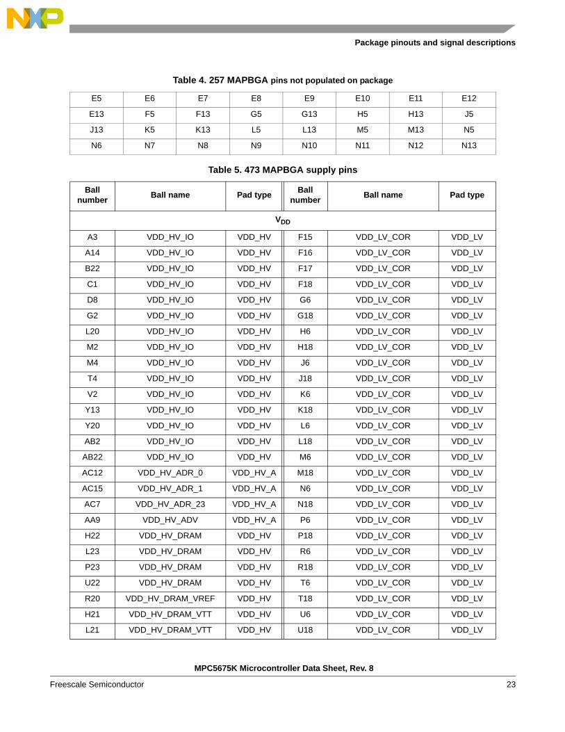
2.2.2 Power supply and reference voltage pinsTable 3 shows the supply pins for the MPC5675K in the 257 MAPBGA package. Table 5 shows the supply pins for the MPC5675K in the 473 MAPBGA package.
Table 4 and Table 6 show the pins not populated on the MPC5675K 257 MAPBGA and 473 MAPBGA packages, respectively.
DRAM ACC Bidirectional DDR pad. Can be configured to support LPDDR half strength, LPDDR full strength, DDR1, DDR2 half strength, DDR2 full strength, and SDR.
DRAM CLK Differential clock driver.
DRAM DQ Bidirectional DDR pad with integrated ODT. Can be configured to support LPDDR half strength, LPDDR full strength, DDR1, DDR2 half strength, DDR2 full strength, and SDR.
DRAM ODT CTL Enable On Die Termination control.
Analog CMOS Schmitt trigger cell with injection proof analog switch.
Analog Shared CMOS Schmitt trigger cell with two injection-proof analog switches.
Table 3. 257 MAPBGA supply pins
Ball number
Ball name Pad typeBall
number Ball name Pad type
VDD
A3 VDD_HV_IO VDD_HV F9 VDD_LV_COR VDD_LV
A9 VDD_HV_IO VDD_HV F10 VDD_LV_COR VDD_LV
B16 VDD_HV_IO VDD_HV F11 VDD_LV_COR VDD_LV
C1 VDD_HV_IO VDD_HV F12 VDD_LV_COR VDD_LV
G2 VDD_HV_IO VDD_HV G6 VDD_LV_COR VDD_LV
M2 VDD_HV_IO VDD_HV G12 VDD_LV_COR VDD_LV
P10 VDD_HV_IO VDD_HV H6 VDD_LV_COR VDD_LV
P14 VDD_HV_IO VDD_HV H12 VDD_LV_COR VDD_LV
T2 VDD_HV_IO VDD_HV J6 VDD_LV_COR VDD_LV
T16 VDD_HV_IO VDD_HV J12 VDD_LV_COR VDD_LV
L14 VDD_HV_DRAM_VREF VDD_HV K6 VDD_LV_COR VDD_LV
D8 VDD_HV_FLA VDD_HV K12 VDD_LV_COR VDD_LV
M1 VDD_HV_OSC VDD_HV L6 VDD_LV_COR VDD_LV
D14 VDD_HV_PDI VDD_HV L12 VDD_LV_COR VDD_LV
H16 VDD_HV_PDI VDD_HV M6 VDD_LV_COR VDD_LV
U14 VDD_HV_PMU VDD_HV M7 VDD_LV_COR VDD_LV
R7 VDD_HV_ADR_13 VDD_HV_A M8 VDD_LV_COR VDD_LV
Table 2. Pad types (continued)
Pad Type Description

MPC5675K Microcontroller Data Sheet, Rev. 8
Package pinouts and signal descriptions
Freescale Semiconductor22
R9 VDD_HV_ADR_02 VDD_HV_A M9 VDD_LV_COR VDD_LV
U9 VDD_HV_ADV VDD_HV_A M10 VDD_LV_COR VDD_LV
F6 VDD_LV_COR VDD_LV M11 VDD_LV_COR VDD_LV
F7 VDD_LV_COR VDD_LV M12 VDD_LV_COR VDD_LV
F8 VDD_LV_COR VDD_LV P4 VDD_LV_PLL VDD_LV
VSS
A1 VSS_HV_IO VSS_HV G7 VSS_LV_COR VSS_LV
A2 VSS_HV_IO VSS_HV G8 VSS_LV_COR VSS_LV
A16 VSS_HV_IO VSS_HV G9 VSS_LV_COR VSS_LV
A17 VSS_HV_IO VSS_HV G10 VSS_LV_COR VSS_LV
B1 VSS_HV_IO VSS_HV G11 VSS_LV_COR VSS_LV
B2 VSS_HV_IO VSS_HV H7 VSS_LV_COR VSS_LV
B9 VSS_HV_IO VSS_HV H8 VSS_LV_COR VSS_LV
B17 VSS_HV_IO VSS_HV H9 VSS_LV_COR VSS_LV
C3 VSS_HV_IO VSS_HV H10 VSS_LV_COR VSS_LV
D15 VSS_HV_IO VSS_HV H11 VSS_LV_COR VSS_LV
H2 VSS_HV_IO VSS_HV J7 VSS_LV_COR VSS_LV
N2 VSS_HV_IO VSS_HV J8 VSS_LV_COR VSS_LV
P9 VSS_HV_IO VSS_HV J9 VSS_LV_COR VSS_LV
R3 VSS_HV_IO VSS_HV J10 VSS_LV_COR VSS_LV
R15 VSS_HV_IO VSS_HV J11 VSS_LV_COR VSS_LV
T1 VSS_HV_IO VSS_HV K7 VSS_LV_COR VSS_LV
T17 VSS_HV_IO VSS_HV K8 VSS_LV_COR VSS_LV
U1 VSS_HV_IO VSS_HV K9 VSS_LV_COR VSS_LV
U2 VSS_HV_IO VSS_HV K10 VSS_LV_COR VSS_LV
U16 VSS_HV_IO VSS_HV K11 VSS_LV_COR VSS_LV
U17 VSS_HV_IO VSS_HV L7 VSS_LV_COR VSS_LV
D9 VSS_HV_FLA VSS_HV L8 VSS_LV_COR VSS_LV
P1 VSS_HV_OSC VSS_HV L9 VSS_LV_COR VSS_LV
C15 VSS_HV_PDI VSS_HV L10 VSS_LV_COR VSS_LV
J16 VSS_HV_PDI VSS_HV L11 VSS_LV_COR VSS_LV
T9 VSS_HV_ADR_02 VSS_HV_A N4 VSS_LV_PLL VSS_LV
T7 VSS_HV_ADR_13 VSS_HV_A U15 VSS_HV_PMU VSS_LV
U10 VSS_HV_ADV VSS_HV_A
Table 3. 257 MAPBGA supply pins (continued)
Ball number
Ball name Pad typeBall
number Ball name Pad type
Package pinouts and signal descriptions
MPC5675K Microcontroller Data Sheet, Rev. 8
Freescale Semiconductor 23
Table 4. 257 MAPBGA pins not populated on package
E5 E6 E7 E8 E9 E10 E11 E12
E13 F5 F13 G5 G13 H5 H13 J5
J13 K5 K13 L5 L13 M5 M13 N5
N6 N7 N8 N9 N10 N11 N12 N13
Table 5. 473 MAPBGA supply pins
Ball number
Ball name Pad typeBall
number Ball name Pad type
VDD
A3 VDD_HV_IO VDD_HV F15 VDD_LV_COR VDD_LV
A14 VDD_HV_IO VDD_HV F16 VDD_LV_COR VDD_LV
B22 VDD_HV_IO VDD_HV F17 VDD_LV_COR VDD_LV
C1 VDD_HV_IO VDD_HV F18 VDD_LV_COR VDD_LV
D8 VDD_HV_IO VDD_HV G6 VDD_LV_COR VDD_LV
G2 VDD_HV_IO VDD_HV G18 VDD_LV_COR VDD_LV
L20 VDD_HV_IO VDD_HV H6 VDD_LV_COR VDD_LV
M2 VDD_HV_IO VDD_HV H18 VDD_LV_COR VDD_LV
M4 VDD_HV_IO VDD_HV J6 VDD_LV_COR VDD_LV
T4 VDD_HV_IO VDD_HV J18 VDD_LV_COR VDD_LV
V2 VDD_HV_IO VDD_HV K6 VDD_LV_COR VDD_LV
Y13 VDD_HV_IO VDD_HV K18 VDD_LV_COR VDD_LV
Y20 VDD_HV_IO VDD_HV L6 VDD_LV_COR VDD_LV
AB2 VDD_HV_IO VDD_HV L18 VDD_LV_COR VDD_LV
AB22 VDD_HV_IO VDD_HV M6 VDD_LV_COR VDD_LV
AC12 VDD_HV_ADR_0 VDD_HV_A M18 VDD_LV_COR VDD_LV
AC15 VDD_HV_ADR_1 VDD_HV_A N6 VDD_LV_COR VDD_LV
AC7 VDD_HV_ADR_23 VDD_HV_A N18 VDD_LV_COR VDD_LV
AA9 VDD_HV_ADV VDD_HV_A P6 VDD_LV_COR VDD_LV
H22 VDD_HV_DRAM VDD_HV P18 VDD_LV_COR VDD_LV
L23 VDD_HV_DRAM VDD_HV R6 VDD_LV_COR VDD_LV
P23 VDD_HV_DRAM VDD_HV R18 VDD_LV_COR VDD_LV
U22 VDD_HV_DRAM VDD_HV T6 VDD_LV_COR VDD_LV
R20 VDD_HV_DRAM_VREF VDD_HV T18 VDD_LV_COR VDD_LV
H21 VDD_HV_DRAM_VTT VDD_HV U6 VDD_LV_COR VDD_LV
L21 VDD_HV_DRAM_VTT VDD_HV U18 VDD_LV_COR VDD_LV

MPC5675K Microcontroller Data Sheet, Rev. 8
Package pinouts and signal descriptions
Freescale Semiconductor24
D13 VDD_HV_FLA VDD_HV V6 VDD_LV_COR VDD_LV
V1 VDD_HV_OSC VDD_HV V7 VDD_LV_COR VDD_LV
D16 VDD_HV_PDI VDD_HV V8 VDD_LV_COR VDD_LV
D20 VDD_HV_PDI VDD_HV V9 VDD_LV_COR VDD_LV
AC17 VDD_HV_PMU VDD_HV V10 VDD_LV_COR VDD_LV
F6 VDD_LV_COR VDD_LV V11 VDD_LV_COR VDD_LV
F7 VDD_LV_COR VDD_LV V12 VDD_LV_COR VDD_LV
F8 VDD_LV_COR VDD_LV V13 VDD_LV_COR VDD_LV
F9 VDD_LV_COR VDD_LV V14 VDD_LV_COR VDD_LV
F10 VDD_LV_COR VDD_LV V15 VDD_LV_COR VDD_LV
F11 VDD_LV_COR VDD_LV V16 VDD_LV_COR VDD_LV
F12 VDD_LV_COR VDD_LV V17 VDD_LV_COR VDD_LV
F13 VDD_LV_COR VDD_LV V18 VDD_LV_COR VDD_LV
F14 VDD_LV_COR VDD_LV Y4 VDD_LV_PLL VDD_LV
VSS
A2 VSS_HV_IO VSS_HV L7 VSS_LV_COR VSS_LV
A22 VSS_HV_IO VSS_HV L8 VSS_LV_COR VSS_LV
A23 VSS_HV_IO VSS_HV L9 VSS_LV_COR VSS_LV
B1 VSS_HV_IO VSS_HV L10 VSS_LV_COR VSS_LV
B2 VSS_HV_IO VSS_HV L11 VSS_LV_COR VSS_LV
B14 VSS_HV_IO VSS_HV L12 VSS_LV_COR VSS_LV
B23 VSS_HV_IO VSS_HV L13 VSS_LV_COR VSS_LV
C3 VSS_HV_IO VSS_HV L14 VSS_LV_COR VSS_LV
D9 VSS_HV_IO VSS_HV L15 VSS_LV_COR VSS_LV
D11 VSS_HV_IO VSS_HV L16 VSS_LV_COR VSS_LV
H2 VSS_HV_IO VSS_HV L17 VSS_LV_COR VSS_LV
K20 VSS_HV_IO VSS_HV M7 VSS_LV_COR VSS_LV
L4 VSS_HV_IO VSS_HV M8 VSS_LV_COR VSS_LV
N2 VSS_HV_IO VSS_HV M9 VSS_LV_COR VSS_LV
A1 VSS_HV_IO VSS_HV M10 VSS_LV_COR VSS_LV
R4 VSS_HV_IO VSS_HV M11 VSS_LV_COR VSS_LV
W2 VSS_HV_IO VSS_HV M12 VSS_LV_COR VSS_LV
Y12 VSS_HV_IO VSS_HV M13 VSS_LV_COR VSS_LV
AA3 VSS_HV_IO VSS_HV M14 VSS_LV_COR VSS_LV
Table 5. 473 MAPBGA supply pins (continued)
Ball number
Ball name Pad typeBall
number Ball name Pad type

Package pinouts and signal descriptions
MPC5675K Microcontroller Data Sheet, Rev. 8
Freescale Semiconductor 25
AA21 VSS_HV_IO VSS_HV M15 VSS_LV_COR VSS_LV
AB1 VSS_HV_IO VSS_HV M16 VSS_LV_COR VSS_LV
AB23 VSS_HV_IO VSS_HV M17 VSS_LV_COR VSS_LV
AC1 VSS_HV_IO VSS_HV N7 VSS_LV_COR VSS_LV
AC2 VSS_HV_IO VSS_HV N8 VSS_LV_COR VSS_LV
AC22 VSS_HV_IO VSS_HV N9 VSS_LV_COR VSS_LV
AC23 VSS_HV_IO VSS_HV N10 VSS_LV_COR VSS_LV
AC13 VSS_HV_ADR_0 VSS_HV_A N11 VSS_LV_COR VSS_LV
AC16 VSS_HV_ADR_1 VSS_HV_A N12 VSS_LV_COR VSS_LV
AC8 VSS_HV_ADR_23 VSS_HV_A N13 VSS_LV_COR VSS_LV
AA10 VSS_HV_ADV VSS_HV_A N14 VSS_LV_COR VSS_LV
H23 VSS_HV_DRAM VSS_HV N15 VSS_LV_COR VSS_LV
L22 VSS_HV_DRAM VSS_HV N16 VSS_LV_COR VSS_LV
P22 VSS_HV_DRAM VSS_HV N17 VSS_LV_COR VSS_LV
V22 VSS_HV_DRAM VSS_HV P7 VSS_LV_COR VSS_LV
D12 VSS_HV_FLA VSS_HV P8 VSS_LV_COR VSS_LV
Y1 VSS_HV_OSC VSS_HV P9 VSS_LV_COR VSS_LV
C21 VSS_HV_PDI VSS_HV P10 VSS_LV_COR VSS_LV
D17 VSS_HV_PDI VSS_HV P11 VSS_LV_COR VSS_LV
G7 VSS_LV_COR VSS_LV P12 VSS_LV_COR VSS_LV
G8 VSS_LV_COR VSS_LV P13 VSS_LV_COR VSS_LV
G9 VSS_LV_COR VSS_LV P14 VSS_LV_COR VSS_LV
G10 VSS_LV_COR VSS_LV P15 VSS_LV_COR VSS_LV
G11 VSS_LV_COR VSS_LV P16 VSS_LV_COR VSS_LV
G12 VSS_LV_COR VSS_LV P17 VSS_LV_COR VSS_LV
G13 VSS_LV_COR VSS_LV R7 VSS_LV_COR VSS_LV
G14 VSS_LV_COR VSS_LV R8 VSS_LV_COR VSS_LV
G15 VSS_LV_COR VSS_LV R9 VSS_LV_COR VSS_LV
G16 VSS_LV_COR VSS_LV R10 VSS_LV_COR VSS_LV
G17 VSS_LV_COR VSS_LV R11 VSS_LV_COR VSS_LV
H7 VSS_LV_COR VSS_LV R12 VSS_LV_COR VSS_LV
H8 VSS_LV_COR VSS_LV R13 VSS_LV_COR VSS_LV
H9 VSS_LV_COR VSS_LV R14 VSS_LV_COR VSS_LV
H10 VSS_LV_COR VSS_LV R15 VSS_LV_COR VSS_LV
Table 5. 473 MAPBGA supply pins (continued)
Ball number
Ball name Pad typeBall
number Ball name Pad type
MPC5675K Microcontroller Data Sheet, Rev. 8
Package pinouts and signal descriptions
Freescale Semiconductor26
H11 VSS_LV_COR VSS_LV R16 VSS_LV_COR VSS_LV
H12 VSS_LV_COR VSS_LV R17 VSS_LV_COR VSS_LV
H13 VSS_LV_COR VSS_LV T7 VSS_LV_COR VSS_LV
H14 VSS_LV_COR VSS_LV T8 VSS_LV_COR VSS_LV
H15 VSS_LV_COR VSS_LV T9 VSS_LV_COR VSS_LV
H16 VSS_LV_COR VSS_LV T10 VSS_LV_COR VSS_LV
H17 VSS_LV_COR VSS_LV T11 VSS_LV_COR VSS_LV
J7 VSS_LV_COR VSS_LV T12 VSS_LV_COR VSS_LV
J8 VSS_LV_COR VSS_LV T13 VSS_LV_COR VSS_LV
J9 VSS_LV_COR VSS_LV T14 VSS_LV_COR VSS_LV
J10 VSS_LV_COR VSS_LV T15 VSS_LV_COR VSS_LV
J11 VSS_LV_COR VSS_LV T16 VSS_LV_COR VSS_LV
J12 VSS_LV_COR VSS_LV T17 VSS_LV_COR VSS_LV
J13 VSS_LV_COR VSS_LV U7 VSS_LV_COR VSS_LV
J14 VSS_LV_COR VSS_LV U8 VSS_LV_COR VSS_LV
J15 VSS_LV_COR VSS_LV U9 VSS_LV_COR VSS_LV
J16 VSS_LV_COR VSS_LV U10 VSS_LV_COR VSS_LV
J17 VSS_LV_COR VSS_LV U11 VSS_LV_COR VSS_LV
K7 VSS_LV_COR VSS_LV U12 VSS_LV_COR VSS_LV
K8 VSS_LV_COR VSS_LV U13 VSS_LV_COR VSS_LV
K9 VSS_LV_COR VSS_LV U14 VSS_LV_COR VSS_LV
K10 VSS_LV_COR VSS_LV U15 VSS_LV_COR VSS_LV
K11 VSS_LV_COR VSS_LV U16 VSS_LV_COR VSS_LV
K12 VSS_LV_COR VSS_LV U17 VSS_LV_COR VSS_LV
K13 VSS_LV_COR VSS_LV W4 VSS_LV_PLL VSS_LV
K14 VSS_LV_COR VSS_LV AC19 VSS_HV_PMU VSS_LV
K15 VSS_LV_COR VSS_LV D5 RESERVED VSS_HV
K16 VSS_LV_COR VSS_LV AB20 RESERVED VSS_HV
K17 VSS_LV_COR VSS_LV
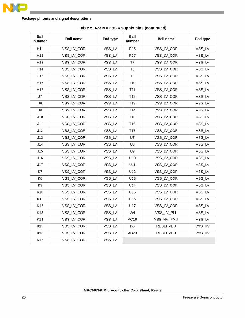
Table 5. 473 MAPBGA supply pins (continued)
Ball number
Ball name Pad typeBall
number Ball name Pad type
Package pinouts and signal descriptions
MPC5675K Microcontroller Data Sheet, Rev. 8
Freescale Semiconductor 27
2.2.3 System pinsTable 7 shows the system pins for the MPC5675K in the 257 MAPBGA package. Table 8 shows the system pins for the MPC5675K in the 473 MAPBGA package.
Table 6. 473 MAPBGA pins not populated on package
E5 E6 E7 E8 E9 E10 E11 E12
E13 E14 E15 E16 E17 E18 E19 F5
F19 G5 G19 H5 H19 J5 J19 K5
K19 L5 L19 M5 M19 N5 N19 P5
P19 R5 R19 T5 T19 U5 U19 V5
V19 W5 W6 W7 W8 W9 W10 W11
W12 W13 W14 W15 W16 W17 W18 W19
Table 7. 257 MAPBGA system pins
Ballnumber
Ball nameWeak pull
during resetSafe mode
default conditionPad type Power domain
C4 FCCU_F[1] disabled not available GP Slow/Medium VDD_HV_IO
C10 JCOMP pulldown not available GP Slow VDD_HV_IO
E1 Nexus MDO[0]1
1 Do not connect pin directly to a power supply or ground.
— not available GP Slow/Fast VDD_HV_IO
E4 NMI pullup not available GP Slow VDD_HV_IO
L15 TCK2
2 If LBIST is enabled, an external pull between 1K and 100K ohm must be connected from TCK to either power or ground to avoid LBIST failures.
pullup not available GP Slow VDD_HV_IO
M16 TMS pullup not available GP Slow VDD_HV_IO
N1 XTALIN — not available Analog Feedthrough VDD_HV_IO
P2 RESET pulldown not available Reset VDD_HV_IO
R1 XTALOUT — not available Analog Feedthrough VDD_HV_IO
R2 FCCU_F[0] disabled not available GP Slow/Medium VDD_HV_IO
R13 VREG_CTRL — — Analog Feedthrough VDD_REG
U12 VREG_INT_ENABLE — — Analog Feedthrough VDD_HV_IO
U13 RESET_SUP pulldown — Analog Feedthrough VDD_HV_IO
Table 8. 473 MAPBGA system pins
Ballnumber
Ball nameWeak pull
during resetSafe mode
default conditionPad type Power domain
C4 FCCU_F[1] disabled not available GP Slow/Medium VDD_HV_IO

MPC5675K Microcontroller Data Sheet, Rev. 8
Package pinouts and signal descriptions
Freescale Semiconductor28
D10 JCOMP pulldown not available GP Slow VDD_HV_IO
E1 Nexus MDO[0]1 — not available GP Slow/Fast VDD_HV_IO
E4 NMI pullup not available GP Slow VDD_HV_IO
R232 dramc CLKB — — DRAM CLK VDD_HV_DRAM
T232 dramc CLK disabled — DRAM CLK VDD_HV_DRAM
W1 XTALIN — not available Analog Feedthrough VDD_HV_IO
Y2 RESET pulldown not available Reset VDD_HV_IO
Y19 TCK3 pullup not available GP Slow VDD_HV_IO
AA1 XTALOUT — not available Analog Feedthrough VDD_HV_IO
AA2 FCCU_F[0] disabled not available GP Slow/Medium VDD_HV_IO
AB19 TMS pullup not available GP Slow VDD_HV_IO
AC18 VREG_CTRL — — Analog Feedthrough VDD_REG
AC20 RESET_SUP pulldown — Analog Feedthrough VDD_HV_IO
AC21 VREG_INT_ENABLE — — Analog Feedthrough VDD_HV_IO
1 Do not connect pin directly to a power supply or ground. 2 PCR234 can be used to control the slew rate of DRAM CLK and DRAM CLKB. See the “System Integration Unit
Lite” chapter of the MPC5675K reference manual.3 If LBIST is enabled, an external pull between 1K and 100K ohm must be connected from TCK to either power or
ground to avoid LBIST failures.
Table 8. 473 MAPBGA system pins (continued)
Ballnumber
Ball nameWeak pull
during resetSafe mode
default conditionPad type Power domain

MP
C5
675K M
icroco
ntro
ller Da
ta S
heet, R
ev. 8
Pack
age
pin
ou
ts and
sign
al des
criptio
ns
Fre
escale S
emico
nductor29 2.2.4 Multiplexed pins
Table 9 shows the pin multiplexing for the MPC5675K in the 257 MAPBGA package. Table 10 shows the pin multiplexing for the MPC5675K in the 473 MAPBGA package.
Table 9. 257 MAPBGA pin multiplexing
Ballnumber
Balltype
Ball name Alternate I/O Additional inputs Analog inputsWeak pull
during resetPad type Power domain
A4 GPIO nexusMDO[5]1
A0: siul_GPIO[114]A1: _A2: npc_wrapper_MDO[5]A3: _
I: _I: _I: _
— disabled GP Slow/Fast
VDD_HV_IO
A5 GPIO nexusMDO[7]1
A0: siul_GPIO[112]A1: _A2: npc_wrapper_MDO[7]A3: _
I: _I: _I: _
— disabled GP Slow/Fast
VDD_HV_IO
A6 GPIO nexusMDO[9]1
A0: siul_GPIO[110]A1: _A2: npc_wrapper_MDO[9]A3: _
I: _I: _I: _
— disabled GP Slow/Fast
VDD_HV_IO
A7 GPIO flexrayCB_TX
A0: siul_GPIO[51]A1: flexray_CB_TXA2: _A3: _
I: _I: _I: _
— disabled GP Slow/Symmetric
VDD_HV_IO
A8 GPIO flexrayCA_TR_EN
A0: siul_GPIO[47]A1: flexray_CA_TR_ENA2: _A3: _
I: ctu0_EXT_INI: flexpwm0_EXT_SYNCI: _
— disabled GP Slow/Symmetric
VDD_HV_IO
A10 GPIO fecRXD[2]
A0: siul_GPIO[213]A1: _A2: _A3: dspi2_SOUT
I: fec_RXD[2]I: _I: siul_EIRQ[21]
— disabled GP Slow/Medium
VDD_HV_IO
A11 GPIO fecRX_CLK
A0: siul_GPIO[209]A1: flexray_DBG2A2: etimer2_ETC[2]A3: dspi0_CS6
I: fec_RX_CLKI: _I: siul_EIRQ[25]
— disabled GP Slow/Medium
VDD_HV_IO
A12 GPIO fecRXD[0]
A0: siul_GPIO[211]A1: i2c1_clockA2: _A3: _
I: fec_RXD[0]I: _I: siul_EIRQ[27]
— disabled GP Slow/Medium
VDD_HV_IO

MP
C5
675K M
icroco
ntro
ller Da
ta S
heet, R
ev. 8
Pack
age
pin
ou
ts and
sign
al des
criptio
ns
Fre
escale S
emico
nductor30
A13 GPIO fecMDIO
A0: siul_GPIO[198]A1: fec_MDIOA2: _A3: dspi2_CS0
I: _I: _I: siul_EIRQ[28]
— disabled GP Slow/Medium
VDD_HV_IO
A14 GPIO fecTX_EN
A0: siul_GPIO[200]A1: fec_TX_ENA2: _A3: lin0_TXD
I: _I: _I: _
— disabled GP Slow/Medium
VDD_HV_IO
A15 GPIO fecTXD[3]
A0: siul_GPIO[204]A1: fec_TXD[3]A2: _A3: dspi2_CS2
I: flexpwm1_FAULT[2]I: _I: siul_EIRQ[29]
— disabled GP Slow/Medium
VDD_HV_IO
B3 GPIO mc_cglclk_out
A0: siul_GPIO[22]A1: mc_cgl_clk_outA2: etimer2_ETC[5]A3: _
I: _I: _I: siul_EIRQ[18]
— disabled GP Slow/Fast
VDD_HV_IO
B4 GPIO can1TXD
A0: siul_GPIO[14]A1: can1_TXDA2: _A3: _
I: _I: _I: siul_EIRQ[13]
— disabled GP Slow/Medium
VDD_HV_IO
B5 GPIO nexusMDO[14]1
A0: siul_GPIO[219]A1: _A2: npc_wrapper_MDO[14]A3: can3_TXD
I: _I: _I: _
— disabled GP Slow/Fast
VDD_HV_IO
B6 GPIO dspi2CS1
A0: siul_GPIO[9]A1: dspi2_CS1A2: _A3: _
I: flexpwm0_FAULT[0]I: lin3_RXDI: can2_RXD
— disabled GP Slow/Medium
VDD_HV_IO
B7 GPIO flexrayCB_TR_EN
A0: siul_GPIO[52]A1: flexray_CB_TR_ENA2: _A3: _
I: _I: _I: _
— disabled GP Slow/Symmetric
VDD_HV_IO
B8 GPIO flexrayCA_TX
A0: siul_GPIO[48]A1: flexray_CA_TXA2: _A3: _
I: ctu1_EXT_INI: _I: _
— disabled GP Slow/Symmetric
VDD_HV_IO
Table 9. 257 MAPBGA pin multiplexing (continued)
Ballnumber
Balltype
Ball name Alternate I/O Additional inputs Analog inputsWeak pull
during resetPad type Power domain
Pack
age
pin
ou
ts and
sign
al des
criptio
ns
MP
C5
675K M
icroco
ntro
ller Da
ta S
heet, R
ev. 8
Fre
escale Se
micondu
ctor
31
B10 GPIO fecRXD[3]
A0: siul_GPIO[214]A1: i2c1_dataA2: _A3: _
I: fec_RXD[3]I: _I: _
— disabled GP Slow/Medium
VDD_HV_IO
B11 GPIO fecRX_ER
A0: siul_GPIO[215]A1: _A2: _A3: dspi0_CS1
I: fec_RX_ERI: _I: _
— disabled GP Slow/Medium
VDD_HV_IO
B12 GPIO fecRXD[1]
A0: siul_GPIO[212]A1: dspi1_CS1A2: etimer2_ETC[5]A3: _
I: fec_RXD[1]I: _I: _
— disabled GP Slow/Medium
VDD_HV_IO
B13 GPIO fecTX_ER
A0: siul_GPIO[205]A1: fec_TX_ERA2: dspi2_CS3A3: _
I: flexpwm1_FAULT[3]I: lin0_RXDI: _
— disabled GP Slow/Medium
VDD_HV_IO
B14 GPIO fecTX_CLK
A0: siul_GPIO[207]A1: flexray_DBG0A2: etimer2_ETC[4]A3: dspi0_CS4
I: fec_TX_CLKI: _I: _
— disabled GP Slow/Medium
VDD_HV_IO
B15 GPIO can0TXD
A0: siul_GPIO[16]A1: can0_TXDA2: _A3: sscm_DEBUG[0]
I: _I: _I: siul_EIRQ[15]
— disabled GP Slow/Medium
VDD_HV_IO
C2 GPIO nexusMDO[15]1
A0: siul_GPIO[220]A1: _A2: npc_wrapper_MDO[15]A3: _
I: can3_RXDI: can2_RXDI: _
— disabled GP Slow/Fast
VDD_HV_IO
C5 GPIO flexrayCB_RX
A0: siul_GPIO[50]A1: _A2: ctu1_EXT_TGRA3: _
I: flexray_CB_RXI: _I: _
— disabled GP Slow/Medium
VDD_HV_IO
C6 GPIO etimer0ETC[0]
A0: siul_GPIO[0]A1: etimer0_ETC[0]A2: _A3: _
I: dspi2_SINI: _I: siul_EIRQ[0]
— disabled GP Slow/Medium
VDD_HV_IO
Table 9. 257 MAPBGA pin multiplexing (continued)
Ballnumber
Balltype
Ball name Alternate I/O Additional inputs Analog inputsWeak pull
during resetPad type Power domain

MP
C5
675K M
icroco
ntro
ller Da
ta S
heet, R
ev. 8
Pack
age
pin
ou
ts and
sign
al des
criptio
ns
Fre
escale S
emico
nductor32
C7 GPIO etimer0ETC[1]
A0: siul_GPIO[1]A1: etimer0_ETC[1]A2: _A3: _
I: _I: _I: siul_EIRQ[1]
— disabled GP Slow/Medium
VDD_HV_IO
C8 GPIO etimer0ETC[2]
A0: siul_GPIO[2]A1: etimer0_ETC[2]A2: _A3: _
I: _I: _I: siul_EIRQ[2]
— disabled GP Slow/Medium
VDD_HV_IO
C9 GPIO etimer0ETC[3]
A0: siul_GPIO[3]A1: etimer0_ETC[3]A2: _A3: _
I: _I: mc_rgm_ABS[2]I: siul_EIRQ[3]
— pulldown GP Slow/Medium
VDD_HV_IO
C11 GPIO fecCRS
A0: siul_GPIO[208]A1: flexray_DBG1A2: etimer2_ETC[3]A3: dspi0_CS5
I: fec_CRSI: _I: _
— disabled GP Slow/Medium
VDD_HV_IO
C12 GPIO fecTXD[0]
A0: siul_GPIO[201]A1: fec_TXD[0]A2: etimer2_ETC[1]A3: _
I: _I: _I: _
— disabled GP Slow/Medium
VDD_HV_IO
C13 GPIO fecCOL
A0: siul_GPIO[206]A1: fec_COLA2: _A3: lin1_TXD
I: _I: _I: _
— disabled GP Slow/Medium
VDD_HV_IO
C14 GPIO can0RXD
A0: siul_GPIO[17]A1: _A2: _A3: sscm_DEBUG[1]
I: can0_RXDI: can1_RXDI: siul_EIRQ[16]
— disabled GP Slow/Medium
VDD_HV_IO
C16 GPIO pdiDATA[5]
A0: siul_GPIO[136]A1: flexpwm2_A[0]A2: _A3: etimer1_ETC[0]
I: pdi_DATA[5]I: _I: _
— disabled PDI Medium
VDD_HV_PDI
C17 GPIO pdiCLOCK
A0: siul_GPIO[128]A1: flexpwm2_B[1]A2: _A3: etimer1_ETC[3]
I: pdi_CLOCKI: _I: _
— disabled PDI Medium
VDD_HV_PDI
Table 9. 257 MAPBGA pin multiplexing (continued)
Ballnumber
Balltype
Ball name Alternate I/O Additional inputs Analog inputsWeak pull
during resetPad type Power domain

MP
C5
675K M
icroco
ntro
ller Da
ta S
heet, R
ev. 8
Pack
age
pin
ou
ts and
sign
al des
criptio
ns
Fre
escale S
emico
nductor33
D1 GPIO nexusMDO[2]1
A0: siul_GPIO[85]A1: _A2: npc_wrapper_MDO[2]A3: _
I: _I: _I: _
— disabled GP Slow/Fast
VDD_HV_IO
D2 GPIO nexusMDO[3]1
A0: siul_GPIO[84]A1: _A2: npc_wrapper_MDO[3]A3: _
I: _I: _I: _
— disabled GP Slow/Fast
VDD_HV_IO
D3 GPIO can1RXD
A0: siul_GPIO[15]A1: _A2: _A3: _
I: can1_RXDI: can0_RXDI: siul_EIRQ[14]
— disabled GP Slow/Medium
VDD_HV_IO
D4 GPIO dspi0SOUT
A0: siul_GPIO[38]A1: dspi0_SOUTA2: _A3: sscm_DEBUG[6]
I: _I: _I: siul_EIRQ[24]
— disabled GP Slow/Medium
VDD_HV_IO
D6 GPIO etimer0ETC[5]
A0: siul_GPIO[44]A1: etimer0_ETC[5]A2: _A3: _
I: _I: _I: _
— disabled GP Slow/Medium
VDD_HV_IO
D7 GPIO etimer0ETC[4]
A0: siul_GPIO[43]A1: etimer0_ETC[4]A2: _A3: _
I: _I: mc_rgm_ABS[0]I: _
— pulldown GP Slow/Medium
VDD_HV_IO
D10 GPIO fecTXD[2]
A0: siul_GPIO[203]A1: fec_TXD[2]A2: _A3: _
I: flexpwm1_FAULT[1]I: _I: _
— disabled GP Slow/Medium
VDD_HV_IO
D11 GPIO fecTXD[1]
A0: siul_GPIO[202]A1: fec_TXD[1]A2: _A3: dspi2_SCK
I: flexpwm1_FAULT[0]I: _I: _
— disabled GP Slow/Medium
VDD_HV_IO
D12 GPIO fecRX_DV
A0: siul_GPIO[210]A1: flexray_DBG3A2: etimer2_ETC[0]A3: dspi0_CS7
I: fec_RX_DVI: _I: _
— disabled GP Slow/Medium
VDD_HV_IO
Table 9. 257 MAPBGA pin multiplexing (continued)
Ballnumber
Balltype
Ball name Alternate I/O Additional inputs Analog inputsWeak pull
during resetPad type Power domain
MP
C5
675K M
icroco
ntro
ller Da
ta S
heet, R
ev. 8
Pack
age
pin
ou
ts and
sign
al des
criptio
ns
Fre
escale S
emico
nductor34
D13 GPIO fecMDC
A0: siul_GPIO[199]A1: fec_MDCA2: _A3: _
I: _I: lin1_RXDI: _
— disabled GP Slow/Medium
VDD_HV_IO
D16 GPIO pdiDATA[0]
A0: siul_GPIO[131]A1: _A2: lin3_TXDA3: _
I: pdi_DATA[0]I: _I: flexpwm2_FAULT[2]
— disabled PDI Medium
VDD_HV_PDI
D17 GPIO pdiDATA[1]
A0: siul_GPIO[132]A1: flexpwm2_B[3]A2: _A3: _
I: pdi_DATA[1]I: _I: _
— disabled PDI Medium
VDD_HV_PDI
E2 GPIO nexusMDO[1]1
A0: siul_GPIO[86]A1: _A2: npc_wrapper_MDO[1]A3: _
I: _I: _I: _
— disabled GP Slow/Fast
VDD_HV_IO
E3 GPIO flexrayCA_RX
A0: siul_GPIO[49]A1: _A2: ctu0_EXT_TGRA3: _
I: flexray_CA_RXI: _I: _
— disabled GP Slow/Medium
VDD_HV_IO
E14 GPIO pdiLINE_V
A0: siul_GPIO[129]A1: _A2: lin2_TXDA3: _
I: pdi_LINE_VI: _I: flexpwm2_FAULT[0]
— disabled PDI Medium
VDD_HV_PDI
E15 GPIO pdiDATA[2]
A0: siul_GPIO[133]A1: flexpwm2_A[1]A2: _A3: etimer1_ETC[2]
I: pdi_DATA[2]I: _I: _
— disabled PDI Medium
VDD_HV_PDI
E16 GPIO pdiDATA[3]
A0: siul_GPIO[134]A1: flexpwm2_X[1]A2: _A3: _
I: pdi_DATA[3]I: _I: _
— disabled PDI Medium
VDD_HV_PDI
E17 GPIO pdiDATA[4]
A0: siul_GPIO[135]A1: flexpwm2_A[2]A2: _A3: etimer1_ETC[4]
I: pdi_DATA[4]I: _I: _
— disabled PDI Medium
VDD_HV_PDI
Table 9. 257 MAPBGA pin multiplexing (continued)
Ballnumber
Balltype
Ball name Alternate I/O Additional inputs Analog inputsWeak pull
during resetPad type Power domain
Pack
age
pin
ou
ts and
sign
al des
criptio
ns
MP
C5
675K M
icroco
ntro
ller Da
ta S
heet, R
ev. 8
Fre
escale Se
micondu
ctor
35
F1 GPIO nexusMDO[6]1
A0: siul_GPIO[113]A1: _A2: npc_wrapper_MDO[6]A3: _
I: _I: _I: _
— disabled GP Slow/Fast
VDD_HV_IO
F2 GPIO nexusMDO[11]1
A0: siul_GPIO[108]A1: _A2: npc_wrapper_MDO[11]A3: _
I: _I: _I: _
— disabled GP Slow/Fast
VDD_HV_IO
F3 GPIO dspi1SOUT
A0: siul_GPIO[7]A1: dspi1_SOUTA2: _A3: _
I: _I: _I: siul_EIRQ[7]
— disabled GP Slow/Medium
VDD_HV_IO
F4 GPIO dspi1SIN
A0: siul_GPIO[8]A1: _A2: _A3: _
I: dspi1_SINI: _I: siul_EIRQ[8]
— disabled GP Slow/Medium
VDD_HV_IO
F14 GPIO mc_cglclk_out
A0: siul_GPIO[233]A1: mc_cgl_clk_outA2: etimer2_ETC[5]A3: _
I: _I: _I: _
— disabled PDI Fast VDD_HV_PDI
F15 GPIO pdiDATA[6]
A0: siul_GPIO[137]A1: flexpwm2_B[0]A2: _A3: etimer1_ETC[1]
I: pdi_DATA[6]I: _I: _
— disabled PDI Medium
VDD_HV_PDI
F16 GPIO pdiDATA[7]
A0: siul_GPIO[138]A1: flexpwm2_B[2]A2: _A3: etimer1_ETC[5]
I: pdi_DATA[7]I: _I: _
— disabled PDI Medium
VDD_HV_PDI
F17 GPIO pdiDATA[8]
A0: siul_GPIO[139]A1: flexpwm2_A[3]A2: _A3: _
I: pdi_DATA[8]I: _I: _
— disabled PDI Medium
VDD_HV_PDI
G1 GPIO nexusMDO[4]1
A0: siul_GPIO[115]A1: _A2: npc_wrapper_MDO[4]A3: _
I: _I: _I: _
— disabled GP Slow/Fast
VDD_HV_IO
Table 9. 257 MAPBGA pin multiplexing (continued)
Ballnumber
Balltype
Ball name Alternate I/O Additional inputs Analog inputsWeak pull
during resetPad type Power domain

Pack
age
pin
ou
ts and
sign
al des
criptio
ns
MP
C5
675K M
icroco
ntro
ller Da
ta S
heet, R
ev. 8
Fre
escale Se
micondu
ctor
36
G3 GPIO dspi0SCK
A0: siul_GPIO[37]A1: dspi0_SCKA2: _A3: sscm_DEBUG[5]
I: flexpwm0_FAULT[3]I: _I: siul_EIRQ[23]
— disabled GP Slow/Medium
VDD_HV_IO
G4 GPIO dspi1SCK
A0: siul_GPIO[6]A1: dspi1_SCKA2: _A3: _
I: _I: _I: siul_EIRQ[6]
— disabled GP Slow/Medium
VDD_HV_IO
G14 GPIO pdiDATA[9]
A0: siul_GPIO[140]A1: flexpwm2_X[2]A2: _A3: _
I: pdi_DATA[9]I: _I: _
— disabled PDI Medium
VDD_HV_PDI
G15 GPIO pdiDATA[10]
A0: siul_GPIO[141]A1: flexpwm2_X[3]A2: _A3: _
I: pdi_DATA[10]I: _I: _
— disabled PDI Medium
VDD_HV_PDI
G16 GPIO pdiDATA[11]
A0: siul_GPIO[142]A1: flexpwm2_X[0]A2: _A3: _
I: pdi_DATA[11]I: _I: _
— disabled PDI Medium
VDD_HV_PDI
G17 GPIO pdiFRAME_V
A0: siul_GPIO[130]A1: _A2: _A3: _
I: pdi_FRAME_VI: lin2_RXDI: flexpwm2_FAULT[1]
— disabled PDI Medium
VDD_HV_PDI
H1 GPIO nexusMDO[10]1
A0: siul_GPIO[109]A1: _A2: npc_wrapper_MDO[10]A3: _
I: _I: _I: _
— disabled GP Slow/Fast
VDD_HV_IO
H3 GPIO dspi0CS0
A0: siul_GPIO[36]A1: dspi0_CS0A2: _A3: sscm_DEBUG[4]
I: _I: _I: siul_EIRQ[22]
— disabled GP Slow/Medium
VDD_HV_IO
H4 GPIO dspi1CS0
A0: siul_GPIO[5]A1: dspi1_CS0A2: _A3: dspi0_CS7
I: _I: _I: siul_EIRQ[5]
— disabled GP Slow/Medium
VDD_HV_IO
Table 9. 257 MAPBGA pin multiplexing (continued)
Ballnumber
Balltype
Ball name Alternate I/O Additional inputs Analog inputsWeak pull
during resetPad type Power domain

MP
C5
675K M
icroco
ntro
ller Da
ta S
heet, R
ev. 8
Pack
age
pin
ou
ts and
sign
al des
criptio
ns
Fre
escale S
emico
nductor37
H14 GPIO pdiDATA[12]
A0: siul_GPIO[143]A1: _A2: _A3: _
I: pdi_DATA[12]I: lin3_RXDI: flexpwm2_FAULT[3]
— disabled PDI Medium
VDD_HV_PDI
H15 GPIO pdiDATA[13]
A0: siul_GPIO[144]A1: pdi_SENS_SEL[2]A2: ctu1_EXT_TGRA3: _
I: pdi_DATA[13]I: _I: _
— disabled PDI Medium
VDD_HV_PDI
H17 GPIO flexpwm0X[0]
A0: siul_GPIO[194]A1: flexpwm0_X[0]A2: ebi_AD28A3: _
I: _I: _I: _
— disabled DRAM ACC
VDD_HV_IO
J1 GPIO nexusMCKO
A0: siul_GPIO[87]A1: _A2: npc_wrapper_MCKOA3: _
I: _I: _I: _
— disabled GP Slow/Fast
VDD_HV_IO
J2 GPIO nexusMDO[8]1
A0: siul_GPIO[111]A1: _A2: npc_wrapper_MDO[8]A3: _
I: _I: _I: _
— disabled GP Slow/Fast
VDD_HV_IO
J3 GPIO dspi2CS0
A0: siul_GPIO[10]A1: dspi2_CS0A2: _A3: can3_TXD
I: _I: _I: siul_EIRQ[9]
— disabled GP Slow/Medium
VDD_HV_IO
J4 GPIO dspi2CS2
A0: siul_GPIO[42]A1: dspi2_CS2A2: lin3_TXDA3: can2_TXD
I: flexpwm0_FAULT[1]I: _I: _
— disabled GP Slow/Medium
VDD_HV_IO
J14 GPIO pdiDATA[14]
A0: siul_GPIO[145]A1: pdi_SENS_SEL[1]A2: i2c2_clockA3: _
I: pdi_DATA[14]I: _I: _
— disabled PDI Medium
VDD_HV_PDI
J15 GPIO pdiDATA[15]
A0: siul_GPIO[146]A1: pdi_SENS_SEL[0]A2: i2c2_dataA3: _
I: pdi_DATA[15]I: ctu1_EXT_INI: _
— disabled PDI Medium
VDD_HV_PDI
Table 9. 257 MAPBGA pin multiplexing (continued)
Ballnumber
Balltype
Ball name Alternate I/O Additional inputs Analog inputsWeak pull
during resetPad type Power domain

Pack
age
pin
ou
ts and
sign
al des
criptio
ns
MP
C5
675K M
icroco
ntro
ller Da
ta S
heet, R
ev. 8
Fre
escale Se
micondu
ctor
38
J17 GPIO flexpwm0X[1]
A0: siul_GPIO[195]A1: flexpwm0_X[1]A2: ebi_AD29A3: _
I: _I: _I: _
— disabled DRAM ACC
VDD_HV_IO
K1 GPIO nexusMSEO_B[0]1
A0: siul_GPIO[89]A1: _A2: npc_wrapper_MSEO_B[0]A3: _
I: _I: _I: _
— disabled GP Slow/Fast
VDD_HV_IO
K2 GPIO nexusMSEO_B[1]1
A0: siul_GPIO[88]A1: _A2: npc_wrapper_MSEO_B[1]A3: _
I: _I: _I: _
— disabled GP Slow/Fast
VDD_HV_IO
K3 GPIO nexusRDY_B
A0: siul_GPIO[216]A1: _A2: nexus_RDY_BA3: _
I: _I: _I: _
— disabled GP Slow/Fast
VDD_HV_IO
K4 GPIO dspi0SIN
A0: siul_GPIO[39]A1: _A2: _A3: sscm_DEBUG[7]
I: dspi0_SINI: _I: _
— disabled GP Slow/Medium
VDD_HV_IO
K14 GPIO flexpwm0X[2]
A0: siul_GPIO[196]A1: flexpwm0_X[2]A2: ebi_AD30A3: _
I: _I: _I: _
— disabled DRAM ACC
VDD_HV_IO
K15 GPIO flexpwm0X[3]
A0: siul_GPIO[197]A1: flexpwm0_X[3]A2: ebi_AD31A3: _
I: _I: _I: _
— disabled DRAM ACC
VDD_HV_IO
K16 GPIO flexpwm0A[1]
A0: siul_GPIO[149]A1: _A2: ebi_RD_WRA3: flexpwm0_A[1]
I: _I: _I: _
— disabled DRAM ACC
VDD_HV_IO
K17 GPIO flexpwm0B[0]
A0: siul_GPIO[148]A1: _A2: ebi_CLKOUTA3: flexpwm0_B[0]
I: _I: _I: _
— disabled DRAM ACC
VDD_HV_IO
Table 9. 257 MAPBGA pin multiplexing (continued)
Ballnumber
Balltype
Ball name Alternate I/O Additional inputs Analog inputsWeak pull
during resetPad type Power domain
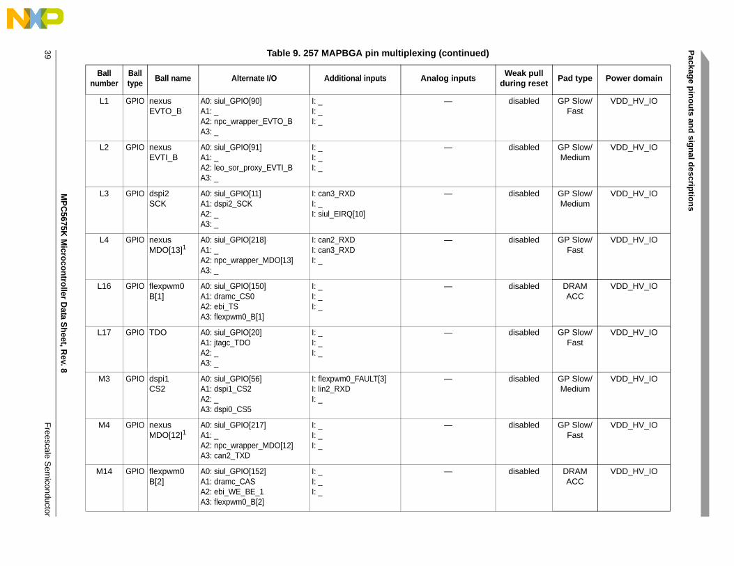
MP
C5
675K M
icroco
ntro
ller Da
ta S
heet, R
ev. 8
Pack
age
pin
ou
ts and
sign
al des
criptio
ns
Fre
escale S
emico
nductor39
L1 GPIO nexusEVTO_B
A0: siul_GPIO[90]A1: _A2: npc_wrapper_EVTO_BA3: _
I: _I: _I: _
— disabled GP Slow/Fast
VDD_HV_IO
L2 GPIO nexusEVTI_B
A0: siul_GPIO[91]A1: _A2: leo_sor_proxy_EVTI_BA3: _
I: _I: _I: _
— disabled GP Slow/Medium
VDD_HV_IO
L3 GPIO dspi2SCK
A0: siul_GPIO[11]A1: dspi2_SCKA2: _A3: _
I: can3_RXDI: _I: siul_EIRQ[10]
— disabled GP Slow/Medium
VDD_HV_IO
L4 GPIO nexusMDO[13]1
A0: siul_GPIO[218]A1: _A2: npc_wrapper_MDO[13]A3: _
I: can2_RXDI: can3_RXDI: _
— disabled GP Slow/Fast
VDD_HV_IO
L16 GPIO flexpwm0B[1]
A0: siul_GPIO[150]A1: dramc_CS0A2: ebi_TSA3: flexpwm0_B[1]
I: _I: _I: _
— disabled DRAM ACC
VDD_HV_IO
L17 GPIO TDO A0: siul_GPIO[20]A1: jtagc_TDOA2: _A3: _
I: _I: _I: _
— disabled GP Slow/Fast
VDD_HV_IO
M3 GPIO dspi1CS2
A0: siul_GPIO[56]A1: dspi1_CS2A2: _A3: dspi0_CS5
I: flexpwm0_FAULT[3]I: lin2_RXDI: _
— disabled GP Slow/Medium
VDD_HV_IO
M4 GPIO nexusMDO[12]1
A0: siul_GPIO[217]A1: _A2: npc_wrapper_MDO[12]A3: can2_TXD
I: _I: _I: _
— disabled GP Slow/Fast
VDD_HV_IO
M14 GPIO flexpwm0B[2]
A0: siul_GPIO[152]A1: dramc_CASA2: ebi_WE_BE_1A3: flexpwm0_B[2]
I: _I: _I: _
— disabled DRAM ACC
VDD_HV_IO
Table 9. 257 MAPBGA pin multiplexing (continued)
Ballnumber
Balltype
Ball name Alternate I/O Additional inputs Analog inputsWeak pull
during resetPad type Power domain

Pack
age
pin
ou
ts and
sign
al des
criptio
ns
MP
C5
675K M
icroco
ntro
ller Da
ta S
heet, R
ev. 8
Fre
escale Se
micondu
ctor
40
M15 GPIO TDI A0: siul_GPIO[21]A1: _A2: _A3: _
I: jtagc_TDII: _I: _
— pullup GP Slow/Medium
VDD_HV_IO
M17 GPIO flexpwm1A[1]
A0: siul_GPIO[157]A1: dramc_ODTA2: ebi_CS1A3: flexpwm1_A[1]
I: _I: _I: _
— disabled DRAM ACC
VDD_HV_IO
N3 GPIO dspi0CS3
A0: siul_GPIO[53]A1: dspi0_CS3A2: i2c2_clockA3: _
I: flexpwm0_FAULT[2]I: _I: _
— disabled GP Slow/Medium
VDD_HV_IO
N14 GPIO flexpwm0B[3]
A0: siul_GPIO[154]A1: dramc_BA[0]A2: ebi_WE_BE_3A3: flexpwm0_B[3]
I: _I: _I: _
— disabled DRAM ACC
VDD_HV_IO
N15 GPIO flexpwm0A[2]
A0: siul_GPIO[151]A1: dramc_RASA2: ebi_WE_BE_0A3: flexpwm0_A[2]
I: _I: _I: _
— disabled DRAM ACC
VDD_HV_IO
N16 GPIO flexpwm1A[0]
A0: siul_GPIO[155]A1: dramc_BA[1]A2: ebi_BDIPA3: flexpwm1_A[0]
I: _I: _I: _
— disabled DRAM ACC
VDD_HV_IO
N17 GPIO flexpwm1B[0]
A0: siul_GPIO[156]A1: dramc_BA[2]A2: ebi_CS0A3: flexpwm1_B[0]
I: _I: _I: _
— disabled DRAM ACC
VDD_HV_IO
P3 GPIO dspi0CS2
A0: siul_GPIO[54]A1: dspi0_CS2A2: i2c2_dataA3: _
I: flexpwm0_FAULT[1]I: _I: _
— disabled GP Slow/Medium
VDD_HV_IO
P5 GPIO etimer1ETC[1]
A0: siul_GPIO[45]A1: etimer1_ETC[1]A2: _A3: _
I: ctu0_EXT_INI: flexpwm0_EXT_SYNCI: ctu1_EXT_IN
— disabled GP Slow/Medium
VDD_HV_IO
Table 9. 257 MAPBGA pin multiplexing (continued)
Ballnumber
Balltype
Ball name Alternate I/O Additional inputs Analog inputsWeak pull
during resetPad type Power domain

MP
C5
675K M
icroco
ntro
ller Da
ta S
heet, R
ev. 8
Pack
age
pin
ou
ts and
sign
al des
criptio
ns
Fre
escale S
emico
nductor41
P6 GPIO etimer1ETC[2]
A0: siul_GPIO[46]A1: etimer1_ETC[2]A2: ctu0_EXT_TGRA3: _
I: _I: _I: _
— disabled GP Slow/Medium
VDD_HV_IO
P7 ANA adc0AN[0]
— siul_GPI[23]
lin0_RXD
AN: adc0_AN[0] Analog VDD_HV_ADR02
P8 GPIO etimer1ETC[3]
A0: siul_GPIO[92]A1: etimer1_ETC[3]A2: _A3: _
I: ctu1_EXT_INI: mc_rgm_FABI: siul_EIRQ[30]
— pulldown GP Slow/Medium
VDD_HV_IO
P11 ANA adc0_adc1AN[14]
— siul_GPI[28] AN: adc0_adc1_AN[14] Analog Shared
VDD_HV_ADR02
P12 GPIO etimer1ETC[4]
A0: siul_GPIO[93]A1: etimer1_ETC[4]A2: ctu1_EXT_TGRA3: _
I: _I: _I: siul_EIRQ[31]
— disabled GP Slow/Medium
VDD_HV_IO
P13 GPIO etimer1ETC[5]
A0: siul_GPIO[78]A1: etimer1_ETC[5]A2: _A3: _
I: _I: _I: siul_EIRQ[26]
— disabled GP Slow/Medium
VDD_HV_IO
P15 GPIO flexpwm0A[3]
A0: siul_GPIO[153]A1: dramc_WEBA2: ebi_WE_BE_2A3: flexpwm0_A[3]
I: _I: _I: _
— disabled DRAM ACC
VDD_HV_IO
P16 GPIO flexpwm0A[0]
A0: siul_GPIO[147]A1: dramc_CKEA2: ebi_OEA3: flexpwm0_A[0]
I: _I: _I: _
— disabled DRAM ACC
VDD_HV_IO
P17 GPIO flexpwm1B[1]
A0: siul_GPIO[163]A1: dramc_ADD[5]A2: ebi_ADD13A3: flexpwm1_B[1]
I: _I: _I: _
— disabled DRAM ACC
VDD_HV_IO
Table 9. 257 MAPBGA pin multiplexing (continued)
Ballnumber
Balltype
Ball name Alternate I/O Additional inputs Analog inputsWeak pull
during resetPad type Power domain
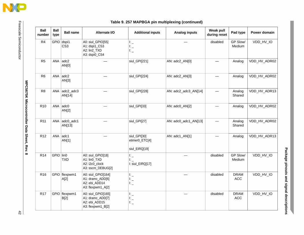
Pack
age
pin
ou
ts and
sign
al des
criptio
ns
MP
C5
675K M
icroco
ntro
ller Da
ta S
heet, R
ev. 8
Fre
escale Se
micondu
ctor
42
R4 GPIO dspi1CS3
A0: siul_GPIO[55]A1: dspi1_CS3A2: lin2_TXDA3: dspi0_CS4
I: _I: _I: _
— disabled GP Slow/Medium
VDD_HV_IO
R5 ANA adc2AN[0]
— siul_GPI[221] AN: adc2_AN[0] — Analog VDD_HV_ADR02
R6 ANA adc2AN[3]
— siul_GPI[224] AN: adc2_AN[3] — Analog VDD_HV_ADR02
R8 ANA adc2_adc3AN[14]
— siul_GPI[228] AN: adc2_adc3_AN[14] — Analog Shared
VDD_HV_ADR13
R10 ANA adc0AN[2]
— siul_GPI[33] AN: adc0_AN[2] — Analog VDD_HV_ADR02
R11 ANA adc0_adc1AN[13]
— siul_GPI[27] AN: adc0_adc1_AN[13] — Analog Shared
VDD_HV_ADR02
R12 ANA adc1AN[1]
— siul_GPI[30]etimer0_ETC[4]
siul_EIRQ[19]
AN: adc1_AN[1] — Analog VDD_HV_ADR13
R14 GPIO lin0TXD
A0: siul_GPIO[18]A1: lin0_TXDA2: i2c0_clockA3: sscm_DEBUG[2]
I: _I: _I: siul_EIRQ[17]
— disabled GP Slow/Medium
VDD_HV_IO
R16 GPIO flexpwm1A[2]
A0: siul_GPIO[164]A1: dramc_ADD[6]A2: ebi_ADD14A3: flexpwm1_A[2]
I: _I: _I: _
— disabled DRAM ACC
VDD_HV_IO
R17 GPIO flexpwm1B[2]
A0: siul_GPIO[165]A1: dramc_ADD[7]A2: ebi_ADD15A3: flexpwm1_B[2]
I: _I: _I: _
— disabled DRAM ACC
VDD_HV_IO
Table 9. 257 MAPBGA pin multiplexing (continued)
Ballnumber
Balltype
Ball name Alternate I/O Additional inputs Analog inputsWeak pull
during resetPad type Power domain

MP
C5
675K M
icroco
ntro
ller Da
ta S
heet, R
ev. 8
Pack
age
pin
ou
ts and
sign
al des
criptio
ns
Fre
escale S
emico
nductor43
T3 GPIO dspi2SOUT
A0: siul_GPIO[12]A1: dspi2_SOUTA2: _A3: _
I: _I: _I: siul_EIRQ[11]
— disabled GP Slow/Medium
VDD_HV_IO
T4 ANA adc3AN[0]
— siul_GPI[229] AN: adc3_AN[0] — Analog VDD_HV_ADR13
T5 ANA adc3AN[3]
— siul_GPI[232] AN: adc3_AN[3] — Analog VDD_HV_ADR13
T6 ANA adc2AN[2]
— siul_GPI[223] AN: adc2_AN[2] — Analog VDD_HV_ADR02
T8 ANA adc2_adc3AN[13]
— siul_GPI[227] AN: adc2_adc3_AN[13] — Analog Shared
VDD_HV_ADR02
T10 ANA adc0AN[1]
— siul_GPI[24]etimer0_ETC[5]
AN: adc0_AN[1] — Analog VDD_HV_ADR02
T11 ANA adc0_adc1AN[12]
— siul_GPI[26] AN: adc0_adc1_AN[12] — Analog Shared
VDD_HV_ADR02
T12 ANA adc1AN[0]
— siul_GPI[29]
lin1_RXD
AN: adc1_AN[0] — Analog VDD_HV_ADR13
T13 ANA adc1AN[2]
— siul_GPI[31]
siul_EIRQ[20]
AN: adc1_AN[2] — Analog VDD_HV_ADR13
T14 GPIO lin0RXD
A0: siul_GPIO[19]A1: _A2: i2c0_dataA3: sscm_DEBUG[3]
I: lin0_RXDI: _I: _
— disabled GP Slow/Medium
VDD_HV_IO
Table 9. 257 MAPBGA pin multiplexing (continued)
Ballnumber
Balltype
Ball name Alternate I/O Additional inputs Analog inputsWeak pull
during resetPad type Power domain
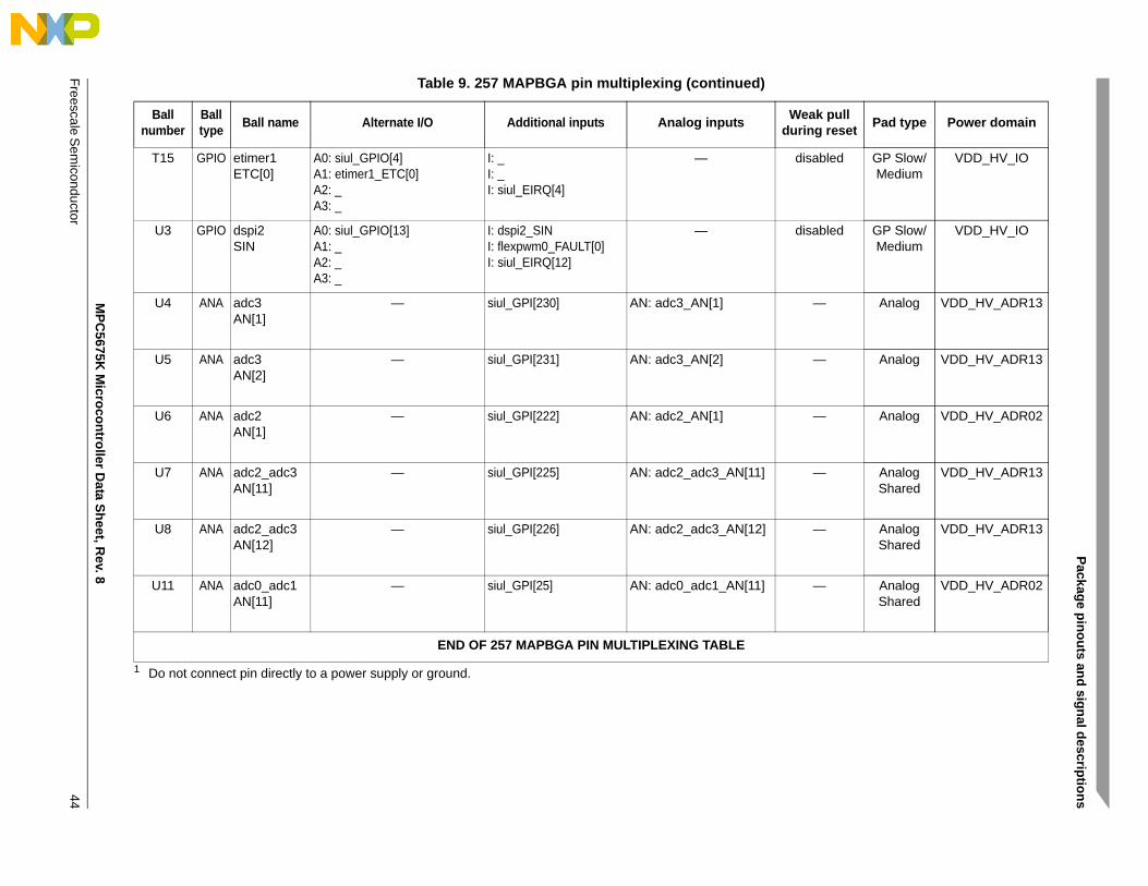
Pack
age
pin
ou
ts and
sign
al des
criptio
ns
MP
C5
675K M
icroco
ntro
ller Da
ta S
heet, R
ev. 8
Fre
escale Se
micondu
ctor
44
T15 GPIO etimer1ETC[0]
A0: siul_GPIO[4]A1: etimer1_ETC[0]A2: _A3: _
I: _I: _I: siul_EIRQ[4]
— disabled GP Slow/Medium
VDD_HV_IO
U3 GPIO dspi2SIN
A0: siul_GPIO[13]A1: _A2: _A3: _
I: dspi2_SINI: flexpwm0_FAULT[0]I: siul_EIRQ[12]
— disabled GP Slow/Medium
VDD_HV_IO
U4 ANA adc3AN[1]
— siul_GPI[230] AN: adc3_AN[1] — Analog VDD_HV_ADR13
U5 ANA adc3AN[2]
— siul_GPI[231] AN: adc3_AN[2] — Analog VDD_HV_ADR13
U6 ANA adc2AN[1]
— siul_GPI[222] AN: adc2_AN[1] — Analog VDD_HV_ADR02
U7 ANA adc2_adc3AN[11]
— siul_GPI[225] AN: adc2_adc3_AN[11] — Analog Shared
VDD_HV_ADR13
U8 ANA adc2_adc3AN[12]
— siul_GPI[226] AN: adc2_adc3_AN[12] — Analog Shared
VDD_HV_ADR13
U11 ANA adc0_adc1AN[11]
— siul_GPI[25] AN: adc0_adc1_AN[11] — Analog Shared
VDD_HV_ADR02
END OF 257 MAPBGA PIN MULTIPLEXING TABLE
1 Do not connect pin directly to a power supply or ground.
Table 9. 257 MAPBGA pin multiplexing (continued)
Ballnumber
Balltype
Ball name Alternate I/O Additional inputs Analog inputsWeak pull
during resetPad type Power domain
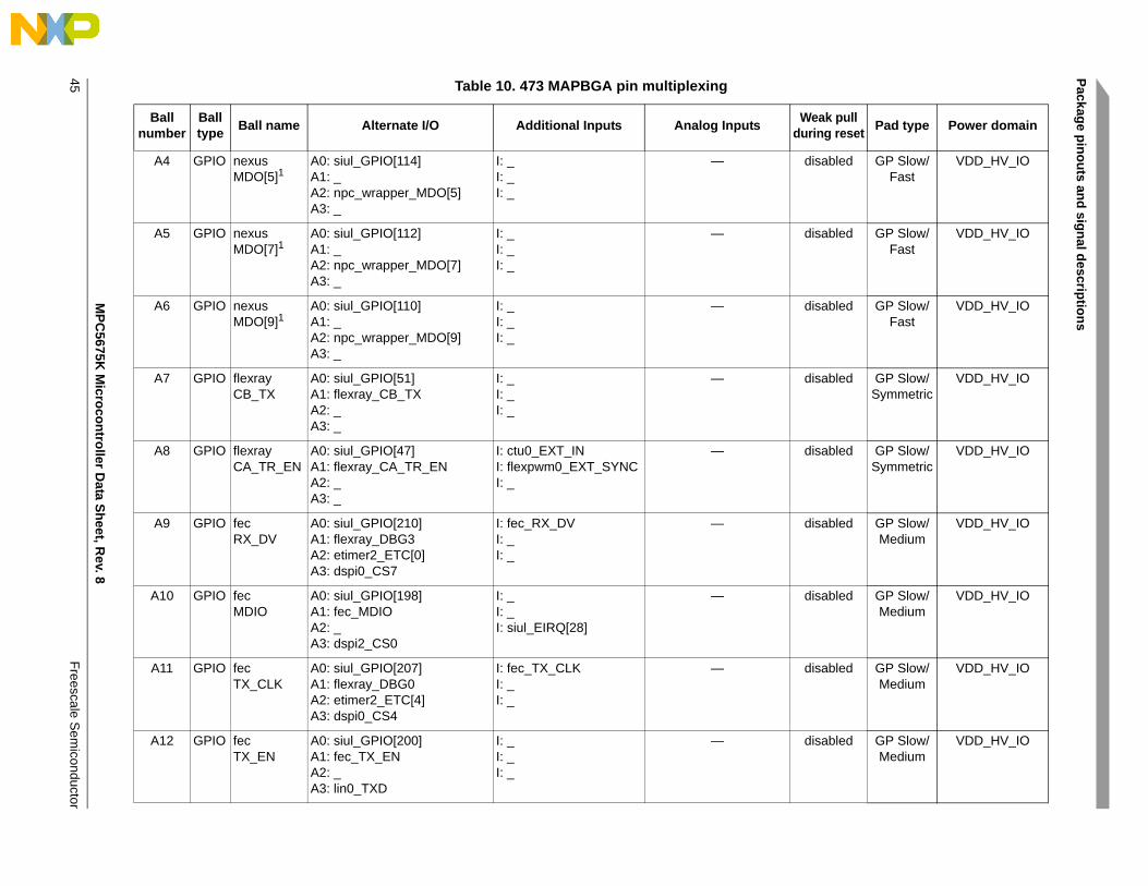
MP
C5
675K M
icroco
ntro
ller Da
ta S
heet, R
ev. 8
Pack
age
pin
ou
ts and
sign
al des
criptio
ns
Fre
escale S
emico
nductor45 Table 10. 473 MAPBGA pin multiplexing
Ballnumber
Balltype
Ball name Alternate I/O Additional Inputs Analog InputsWeak pull
during resetPad type Power domain
A4 GPIO nexusMDO[5]1
A0: siul_GPIO[114]A1: _A2: npc_wrapper_MDO[5]A3: _
I: _I: _I: _
— disabled GP Slow/Fast
VDD_HV_IO
A5 GPIO nexusMDO[7]1
A0: siul_GPIO[112]A1: _A2: npc_wrapper_MDO[7]A3: _
I: _I: _I: _
— disabled GP Slow/Fast
VDD_HV_IO
A6 GPIO nexusMDO[9]1
A0: siul_GPIO[110]A1: _A2: npc_wrapper_MDO[9]A3: _
I: _I: _I: _
— disabled GP Slow/Fast
VDD_HV_IO
A7 GPIO flexrayCB_TX
A0: siul_GPIO[51]A1: flexray_CB_TXA2: _A3: _
I: _I: _I: _
— disabled GP Slow/Symmetric
VDD_HV_IO
A8 GPIO flexrayCA_TR_EN
A0: siul_GPIO[47]A1: flexray_CA_TR_ENA2: _A3: _
I: ctu0_EXT_INI: flexpwm0_EXT_SYNCI: _
— disabled GP Slow/Symmetric
VDD_HV_IO
A9 GPIO fecRX_DV
A0: siul_GPIO[210]A1: flexray_DBG3A2: etimer2_ETC[0]A3: dspi0_CS7
I: fec_RX_DVI: _I: _
— disabled GP Slow/Medium
VDD_HV_IO
A10 GPIO fecMDIO
A0: siul_GPIO[198]A1: fec_MDIOA2: _A3: dspi2_CS0
I: _I: _I: siul_EIRQ[28]
— disabled GP Slow/Medium
VDD_HV_IO
A11 GPIO fecTX_CLK
A0: siul_GPIO[207]A1: flexray_DBG0A2: etimer2_ETC[4]A3: dspi0_CS4
I: fec_TX_CLKI: _I: _
— disabled GP Slow/Medium
VDD_HV_IO
A12 GPIO fecTX_EN
A0: siul_GPIO[200]A1: fec_TX_ENA2: _A3: lin0_TXD
I: _I: _I: _
— disabled GP Slow/Medium
VDD_HV_IO

Pack
age
pin
ou
ts and
sign
al des
criptio
ns
MP
C5
675K M
icroco
ntro
ller Da
ta S
heet, R
ev. 8
Fre
escale Se
micondu
ctor
46
A13 GPIO fecTXD[3]
A0: siul_GPIO[204]A1: fec_TXD[3]A2: _A3: dspi2_CS2
I: flexpwm1_FAULT[2]I: _I: siul_EIRQ[29]
— disabled GP Slow/Medium
VDD_HV_IO
A15 GPIO pdiDATA[3]
A0: siul_GPIO[134]A1: flexpwm2_X[1]A2: _A3: _
I: pdi_DATA[3]I: _I: _
— disabled PDI Medium
VDD_HV_PDI
A16 GPIO pdiDATA[1]
A0: siul_GPIO[132]A1: flexpwm2_B[3]A2: _A3: _
I: pdi_DATA[1]I: _I: _
— disabled PDI Medium
VDD_HV_PDI
A17 GPIO pdiCLOCK
A0: siul_GPIO[128]A1: flexpwm2_B[1]A2: _A3: etimer1_ETC[3]
I: pdi_CLOCKI: _I: _
— disabled PDI Medium
VDD_HV_PDI
A18 GPIO pdiDATA[7]
A0: siul_GPIO[138]A1: flexpwm2_B[2]A2: _A3: etimer1_ETC[5]
I: pdi_DATA[7]I: _I: _
— disabled PDI Medium
VDD_HV_PDI
A19 GPIO pdiDATA[10]
A0: siul_GPIO[141]A1: flexpwm2_X[3]A2: _A3: _
I: pdi_DATA[10]I: _I: _
— disabled PDI Medium
VDD_HV_PDI
A20 GPIO pdiDATA[13]
A0: siul_GPIO[144]A1: pdi_SENS_SEL[2]A2: ctu1_EXT_TGRA3: _
I: pdi_DATA[13]I: _I: _
— disabled PDI Medium
VDD_HV_PDI
A21 GPIO pdiDATA[15]
A0: siul_GPIO[146]A1: pdi_SENS_SEL[0]A2: i2c2_dataA3: _
I: pdi_DATA[15]I: ctu1_EXT_INI: _
— disabled PDI Medium
VDD_HV_PDI
B3 GPIO mc_cglclk_out
A0: siul_GPIO[22]A1: mc_cgl_clk_outA2: etimer2_ETC[5]A3: _
I: _I: _I: siul_EIRQ[18]
— disabled GP Slow/Fast
VDD_HV_IO
Table 10. 473 MAPBGA pin multiplexing (continued)
Ballnumber
Balltype
Ball name Alternate I/O Additional Inputs Analog InputsWeak pull
during resetPad type Power domain
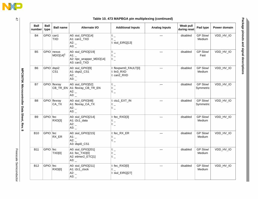
MP
C5
675K M
icroco
ntro
ller Da
ta S
heet, R
ev. 8
Pack
age
pin
ou
ts and
sign
al des
criptio
ns
Fre
escale S
emico
nductor47
B4 GPIO can1TXD
A0: siul_GPIO[14]A1: can1_TXDA2: _A3: _
I: _I: _I: siul_EIRQ[13]
— disabled GP Slow/Medium
VDD_HV_IO
B5 GPIO nexusMDO[14]1
A0: siul_GPIO[219]A1: _A2: npc_wrapper_MDO[14]A3: can3_TXD
I: _I: _I: _
— disabled GP Slow/Fast
VDD_HV_IO
B6 GPIO dspi2CS1
A0: siul_GPIO[9]A1: dspi2_CS1A2: _A3: _
I: flexpwm0_FAULT[0]I: lin3_RXDI: can2_RXD
— disabled GP Slow/Medium
VDD_HV_IO
B7 GPIO flexrayCB_TR_EN
A0: siul_GPIO[52]A1: flexray_CB_TR_ENA2: _A3: _
I: _I: _I: _
— disabled GP Slow/Symmetric
VDD_HV_IO
B8 GPIO flexrayCA_TX
A0: siul_GPIO[48]A1: flexray_CA_TXA2: _A3: _
I: ctu1_EXT_INI: _I: _
— disabled GP Slow/Symmetric
VDD_HV_IO
B9 GPIO fecRXD[3]
A0: siul_GPIO[214]A1: i2c1_dataA2: _A3: _
I: fec_RXD[3]I: _I: _
— disabled GP Slow/Medium
VDD_HV_IO
B10 GPIO fecRX_ER
A0: siul_GPIO[215]A1: _A2: _A3: dspi0_CS1
I: fec_RX_ERI: _I: _
— disabled GP Slow/Medium
VDD_HV_IO
B11 GPIO fecTXD[0]
A0: siul_GPIO[201]A1: fec_TXD[0]A2: etimer2_ETC[1]A3: _
I: _I: _I: _
— disabled GP Slow/Medium
VDD_HV_IO
B12 GPIO fecRXD[0]
A0: siul_GPIO[211]A1: i2c1_clockA2: _A3: _
I: fec_RXD[0]I: _I: siul_EIRQ[27]
— disabled GP Slow/Medium
VDD_HV_IO
Table 10. 473 MAPBGA pin multiplexing (continued)
Ballnumber
Balltype
Ball name Alternate I/O Additional Inputs Analog InputsWeak pull
during resetPad type Power domain

Pack
age
pin
ou
ts and
sign
al des
criptio
ns
MP
C5
675K M
icroco
ntro
ller Da
ta S
heet, R
ev. 8
Fre
escale Se
micondu
ctor
48
B13 GPIO fecTX_ER
A0: siul_GPIO[205]A1: fec_TX_ERA2: dspi2_CS3A3: _
I: flexpwm1_FAULT[3]I: lin0_RXDI: _
— disabled GP Slow/Medium
VDD_HV_IO
B15 GPIO pdiDATA[6]
A0: siul_GPIO[137]A1: flexpwm2_B[0]A2: _A3: etimer1_ETC[1]
I: pdi_DATA[6]I: _I: _
— disabled PDI Medium
VDD_HV_PDI
B16 GPIO pdiDATA[4]
A0: siul_GPIO[135]A1: flexpwm2_A[2]A2: _A3: etimer1_ETC[4]
I: pdi_DATA[4]I: _I: _
— disabled PDI Medium
VDD_HV_PDI
B17 GPIO pdiDATA[0]
A0: siul_GPIO[131]A1: _A2: lin3_TXDA3: _
I: pdi_DATA[0]I: _I: flexpwm2_FAULT[2]
— disabled PDI Medium
VDD_HV_PDI
B18 GPIO pdiLINE_V
A0: siul_GPIO[129]A1: _A2: lin2_TXDA3: _
I: pdi_LINE_VI: _I: flexpwm2_FAULT[0]
— disabled PDI Medium
VDD_HV_PDI
B19 GPIO pdiDATA[9]
A0: siul_GPIO[140]A1: flexpwm2_X[2]A2: _A3: _
I: pdi_DATA[9]I: _I: _
— disabled PDI Medium
VDD_HV_PDI
B20 GPIO pdiDATA[14]
A0: siul_GPIO[145]A1: pdi_SENS_SEL[1]A2: i2c2_clockA3: _
I: pdi_DATA[14]I: _I: _
— disabled PDI Medium
VDD_HV_PDI
B21 GPIO can0TXD
A0: siul_GPIO[16]A1: can0_TXDA2: _A3: sscm_DEBUG[0]
I: _I: _I: siul_EIRQ[15]
— disabled GP Slow/Medium
VDD_HV_IO
C2 GPIO nexusMDO[15]1
A0: siul_GPIO[220]A1: _A2: npc_wrapper_MDO[15]A3: _
I: can3_RXDI: can2_RXDI: _
— disabled GP Slow/Fast
VDD_HV_IO
Table 10. 473 MAPBGA pin multiplexing (continued)
Ballnumber
Balltype
Ball name Alternate I/O Additional Inputs Analog InputsWeak pull
during resetPad type Power domain

MP
C5
675K M
icroco
ntro
ller Da
ta S
heet, R
ev. 8
Pack
age
pin
ou
ts and
sign
al des
criptio
ns
Fre
escale S
emico
nductor49
C5 GPIO flexrayCB_RX
A0: siul_GPIO[50]A1: _A2: ctu1_EXT_TGRA3: _
I: flexray_CB_RXI: _I: _
— disabled GP Slow/Medium
VDD_HV_IO
C6 GPIO etimer0ETC[4]
A0: siul_GPIO[43]A1: etimer0_ETC[4]A2: _A3: _
I: _I: mc_rgm_ABS[0]I: _
— pulldown GP Slow/Medium
VDD_HV_IO
C7 GPIO etimer0ETC[1]
A0: siul_GPIO[1]A1: etimer0_ETC[1]A2: _A3: _
I: _I: _I: siul_EIRQ[1]
— disabled GP Slow/Medium
VDD_HV_IO
C8 GPIO etimer0ETC[2]
A0: siul_GPIO[2]A1: etimer0_ETC[2]A2: _A3: _
I: _I: _I: siul_EIRQ[2]
— disabled GP Slow/Medium
VDD_HV_IO
C9 GPIO etimer0ETC[3]
A0: siul_GPIO[3]A1: etimer0_ETC[3]A2: _A3: _
I: _I: mc_rgm_ABS[2]I: siul_EIRQ[3]
— pulldown GP Slow/Medium
VDD_HV_IO
C10 GPIO fecTXD[2]
A0: siul_GPIO[203]A1: fec_TXD[2]A2: _A3: _
I: flexpwm1_FAULT[1]I: _I: _
— disabled GP Slow/Medium
VDD_HV_IO
C11 GPIO fecTXD[1]
A0: siul_GPIO[202]A1: fec_TXD[1]A2: _A3: dspi2_SCK
I: flexpwm1_FAULT[0]I: _I: _
— disabled GP Slow/Medium
VDD_HV_IO
C12 GPIO fecCRS
A0: siul_GPIO[208]A1: flexray_DBG1A2: etimer2_ETC[3]A3: dspi0_CS5
I: fec_CRSI: _I: _
— disabled GP Slow/Medium
VDD_HV_IO
C13 GPIO fecRX_CLK
A0: siul_GPIO[209]A1: flexray_DBG2A2: etimer2_ETC[2]A3: dspi0_CS6
I: fec_RX_CLKI: _I: siul_EIRQ[25]
— disabled GP Slow/Medium
VDD_HV_IO
Table 10. 473 MAPBGA pin multiplexing (continued)
Ballnumber
Balltype
Ball name Alternate I/O Additional Inputs Analog InputsWeak pull
during resetPad type Power domain

Pack
age
pin
ou
ts and
sign
al des
criptio
ns
MP
C5
675K M
icroco
ntro
ller Da
ta S
heet, R
ev. 8
Fre
escale Se
micondu
ctor
50
C14 GPIO fecRXD[1]
A0: siul_GPIO[212]A1: dspi1_CS1A2: etimer2_ETC[5]A3: _
I: fec_RXD[1]I: _I: _
— disabled GP Slow/Medium
VDD_HV_IO
C15 GPIO fecCOL
A0: siul_GPIO[206]A1: fec_COLA2: _A3: lin1_TXD
I: _I: _I: _
— disabled GP Slow/Medium
VDD_HV_IO
C16 GPIO pdiDATA[5]
A0: siul_GPIO[136]A1: flexpwm2_A[0]A2: _A3: etimer1_ETC[0]
I: pdi_DATA[5]I: _I: _
— disabled PDI Medium
VDD_HV_PDI
C17 GPIO pdiDATA[2]
A0: siul_GPIO[133]A1: flexpwm2_A[1]A2: _A3: etimer1_ETC[2]
I: pdi_DATA[2]I: _I: _
— disabled PDI Medium
VDD_HV_PDI
C18 GPIO pdiDATA[8]
A0: siul_GPIO[139]A1: flexpwm2_A[3]A2: _A3: _
I: pdi_DATA[8]I: _I: _
— disabled PDI Medium
VDD_HV_PDI
C19 GPIO pdiDATA[12]
A0: siul_GPIO[143]A1: _A2: _A3: _
I: pdi_DATA[12]I: lin3_RXDI: flexpwm2_FAULT[3]
— disabled PDI Medium
VDD_HV_PDI
C20 GPIO can0RXD
A0: siul_GPIO[17]A1: _A2: _A3: sscm_DEBUG[1]
I: can0_RXDI: can1_RXDI: siul_EIRQ[16]
— disabled GP Slow/Medium
VDD_HV_IO
C22 GPIO siulGPIO[197]
A0: siul_GPIO[197]A1: flexpwm0_X[3]A2: ebi_AD31A3: _
I: _I: _I: _
— disabled DRAM ACC
VDD_HV_DRAM
C23 GPIO dramcCAS
A0: siul_GPIO[152]A1: dramc_CASA2: ebi_WE_BE_1A3: flexpwm0_B[2]
I: _I: _I: _
— disabled DRAM ACC
VDD_HV_DRAM
Table 10. 473 MAPBGA pin multiplexing (continued)
Ballnumber
Balltype
Ball name Alternate I/O Additional Inputs Analog InputsWeak pull
during resetPad type Power domain

MP
C5
675K M
icroco
ntro
ller Da
ta S
heet, R
ev. 8
Pack
age
pin
ou
ts and
sign
al des
criptio
ns
Fre
escale S
emico
nductor51
D1 GPIO nexusMDO[1]1
A0: siul_GPIO[86]A1: _A2: npc_wrapper_MDO[1]A3: _
I: _I: _I: _
— disabled GP Slow/Fast
VDD_HV_IO
D2 GPIO nexusMDO[3]1
A0: siul_GPIO[84]A1: _A2: npc_wrapper_MDO[3]A3: _
I: _I: _I: _
— disabled GP Slow/Fast
VDD_HV_IO
D3 GPIO can1RXD
A0: siul_GPIO[15]A1: _A2: _A3: _
I: can1_RXDI: can0_RXDI: siul_EIRQ[14]
— disabled GP Slow/Medium
VDD_HV_IO
D4 GPIO dspi0SOUT
A0: siul_GPIO[38]A1: dspi0_SOUTA2: _A3: sscm_DEBUG[6]
I: _I: _I: siul_EIRQ[24]
— disabled GP Slow/Medium
VDD_HV_IO
D6 GPIO etimer0ETC[5]
A0: siul_GPIO[44]A1: etimer0_ETC[5]A2: _A3: _
I: _I: _I: _
— disabled GP Slow/Medium
VDD_HV_IO
D7 GPIO etimer0ETC[0]
A0: siul_GPIO[0]A1: etimer0_ETC[0]A2: _A3: _
I: dspi2_SINI: _I: siul_EIRQ[0]
— disabled GP Slow/Medium
VDD_HV_IO
D14 GPIO fecRXD[2]
A0: siul_GPIO[213]A1: _A2: _A3: dspi2_SOUT
I: fec_RXD[2]I: _I: siul_EIRQ[21]
— disabled GP Slow/Medium
VDD_HV_IO
D15 GPIO fecMDC
A0: siul_GPIO[199]A1: fec_MDCA2: _A3: _
I: _I: lin1_RXDI: _
— disabled GP Slow/Medium
VDD_HV_IO
D18 GPIO pdiDATA[11]
A0: siul_GPIO[142]A1: flexpwm2_X[0]A2: _A3: _
I: pdi_DATA[11]I: _I: _
— disabled PDI Medium
VDD_HV_PDI
Table 10. 473 MAPBGA pin multiplexing (continued)
Ballnumber
Balltype
Ball name Alternate I/O Additional Inputs Analog InputsWeak pull
during resetPad type Power domain

Pack
age
pin
ou
ts and
sign
al des
criptio
ns
MP
C5
675K M
icroco
ntro
ller Da
ta S
heet, R
ev. 8
Fre
escale Se
micondu
ctor
52
D19 GPIO pdiFRAME_V
A0: siul_GPIO[130]A1: _A2: _A3: _
I: pdi_FRAME_VI: lin2_RXDI: flexpwm2_FAULT[1]
— disabled PDI Medium
VDD_HV_PDI
D21 GPIO dramcBA[1]
A0: siul_GPIO[155]A1: dramc_BA[1]A2: ebi_BDIPA3: flexpwm1_A[0]
I: _I: _I: _
— disabled DRAM ACC
VDD_HV_DRAM
D22 GPIO siulGPIO[195]
A0: siul_GPIO[195]A1: flexpwm0_X[1]A2: ebi_AD29A3: _
I: _I: _I: _
— disabled DRAM ACC
VDD_HV_DRAM
D23 GPIO dramcBA[0]
A0: siul_GPIO[154]A1: dramc_BA[0]A2: ebi_WE_BE_3A3: flexpwm0_B[3]
I: _I: _I: _
— disabled DRAM ACC
VDD_HV_DRAM
E2 GPIO nexusMDO[2]1
A0: siul_GPIO[85]A1: _A2: npc_wrapper_MDO[2]A3: _
I: _I: _I: _
— disabled GP Slow/Fast
VDD_HV_IO
E3 GPIO flexrayCA_RX
A0: siul_GPIO[49]A1: _A2: ctu0_EXT_TGRA3: _
I: flexray_CA_RXI: _I: _
— disabled GP Slow/Medium
VDD_HV_IO
E20 GPIO mc_cglclk_out
A0: siul_GPIO[233]A1: mc_cgl_clk_outA2: etimer2_ETC[5]A3: _
I: _I: _I: _
— disabled PDI Fast VDD_HV_PDI
E21 GPIO siulGPIO[149]
A0: siul_GPIO[149]A1: _A2: ebi_RD_WRA3: flexpwm0_A[1]
I: _I: _I: _
— disabled DRAM ACC
VDD_HV_DRAM
E22 GPIO dramcCS0
A0: siul_GPIO[150]A1: dramc_CS0A2: ebi_TSA3: flexpwm0_B[1]
I: _I: _I: _
— disabled DRAM ACC
VDD_HV_DRAM
Table 10. 473 MAPBGA pin multiplexing (continued)
Ballnumber
Balltype
Ball name Alternate I/O Additional Inputs Analog InputsWeak pull
during resetPad type Power domain

MP
C5
675K M
icroco
ntro
ller Da
ta S
heet, R
ev. 8
Pack
age
pin
ou
ts and
sign
al des
criptio
ns
Fre
escale S
emico
nductor53
E23 GPIO dramcBA[2]
A0: siul_GPIO[156]A1: dramc_BA[2]A2: ebi_CS0A3: flexpwm1_B[0]
I: _I: _I: _
— disabled DRAM ACC
VDD_HV_DRAM
F1 GPIO nexusMDO[10]1
A0: siul_GPIO[109]A1: _A2: npc_wrapper_MDO[10]A3: _
I: _I: _I: _
— disabled GP Slow/Fast
VDD_HV_IO
F2 GPIO nexusMDO[11]1
A0: siul_GPIO[108]A1: _A2: npc_wrapper_MDO[11]A3: _
I: _I: _I: _
— disabled GP Slow/Fast
VDD_HV_IO
F3 GPIO nexusMDO[6]1
A0: siul_GPIO[113]A1: _A2: npc_wrapper_MDO[6]A3: _
I: _I: _I: _
— disabled GP Slow/Fast
VDD_HV_IO
F4 GPIO nexusMDO[4]1
A0: siul_GPIO[115]A1: _A2: npc_wrapper_MDO[4]A3: _
I: _I: _I: _
— disabled GP Slow/Fast
VDD_HV_IO
F20 GPIO dramcRAS
A0: siul_GPIO[151]A1: dramc_RASA2: ebi_WE_BE_0A3: flexpwm0_A[2]
I: _I: _I: _
— disabled DRAM ACC
VDD_HV_DRAM
F21 GPIO siulGPIO[194]
A0: siul_GPIO[194]A1: flexpwm0_X[0]A2: ebi_AD28A3: _
I: _I: _I: _
— disabled DRAM ACC
VDD_HV_DRAM
F22 GPIO siulGPIO[148]
A0: siul_GPIO[148]A1: _A2: ebi_CLKOUTA3: flexpwm0_B[0]
I: _I: _I: _
— disabled DRAM ACC
VDD_HV_DRAM
F23 GPIO dramcD[5]
A0: siul_GPIO[179]A1: dramc_D[5]A2: ebi_AD13A3: ebi_ADD29
I: _I: _I: _
— disabled DRAM DQ VDD_HV_DRAM
Table 10. 473 MAPBGA pin multiplexing (continued)
Ballnumber
Balltype
Ball name Alternate I/O Additional Inputs Analog InputsWeak pull
during resetPad type Power domain

Pack
age
pin
ou
ts and
sign
al des
criptio
ns
MP
C5
675K M
icroco
ntro
ller Da
ta S
heet, R
ev. 8
Fre
escale Se
micondu
ctor
54
G1 GPIO nexusMCKO
A0: siul_GPIO[87]A1: _A2: npc_wrapper_MCKOA3: _
I: _I: _I: _
— disabled GP Slow/Fast
VDD_HV_IO
G3 GPIO nexusMDO[8]1
A0: siul_GPIO[111]A1: _A2: npc_wrapper_MDO[8]A3: _
I: _I: _I: _
— disabled GP Slow/Fast
VDD_HV_IO
G4 GPIO nexusMSEO_B[1]1
A0: siul_GPIO[88]A1: _A2: npc_wrapper_MSEO_B[1]A3: _
I: _I: _I: _
— disabled GP Slow/Fast
VDD_HV_IO
G20 GPIO siulGPIO[196]
A0: siul_GPIO[196]A1: flexpwm0_X[2]A2: ebi_AD30A3: _
I: _I: _I: _
— disabled DRAM ACC
VDD_HV_DRAM
G21 GPIO dramcDQS[0]
A0: siul_GPIO[190]A1: dramc_DQS[0]A2: ebi_AD24A3: _
I: _I: _I: _
— disabled DRAM DQ VDD_HV_DRAM
G22 GPIO dramcDM[0]
A0: siul_GPIO[192]A1: dramc_DM[0]A2: ebi_AD26A3: _
I: _I: _I: _
— disabled DRAM DQ VDD_HV_DRAM
G23 GPIO dramcD[7]
A0: siul_GPIO[181]A1: dramc_D[7]A2: ebi_AD15A3: ebi_ADD31
I: _I: _I: _
— disabled DRAM DQ VDD_HV_DRAM
H1 GPIO nexusEVTO_B
A0: siul_GPIO[90]A1: _A2: npc_wrapper_EVTO_BA3: _
I: _I: _I: _
— disabled GP Slow/Fast
VDD_HV_IO
H3 GPIO nexusMSEO_B[0]1
A0: siul_GPIO[89]A1: _A2: npc_wrapper_MSEO_B[0]A3: _
I: _I: _I: _
— disabled GP Slow/Fast
VDD_HV_IO
Table 10. 473 MAPBGA pin multiplexing (continued)
Ballnumber
Balltype
Ball name Alternate I/O Additional Inputs Analog InputsWeak pull
during resetPad type Power domain
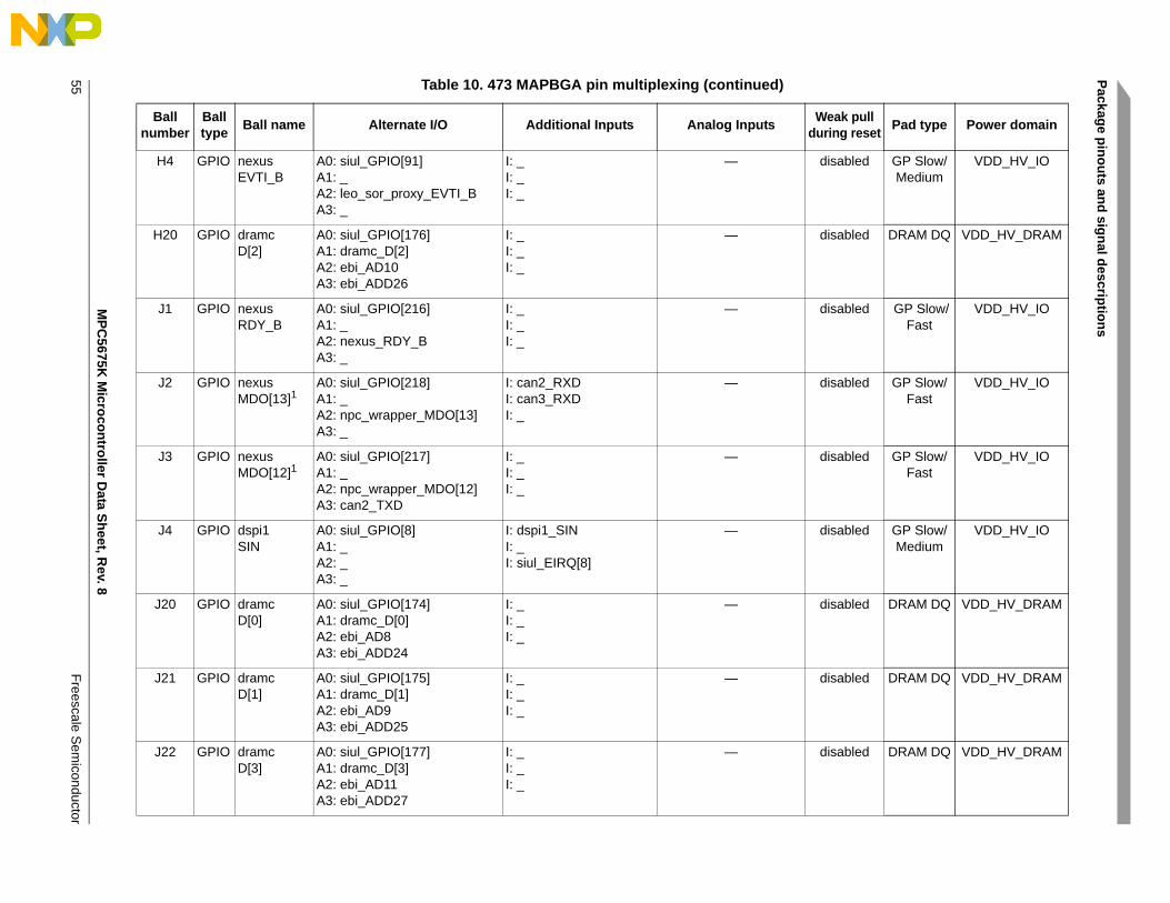
MP
C5
675K M
icroco
ntro
ller Da
ta S
heet, R
ev. 8
Pack
age
pin
ou
ts and
sign
al des
criptio
ns
Fre
escale S
emico
nductor55
H4 GPIO nexusEVTI_B
A0: siul_GPIO[91]A1: _A2: leo_sor_proxy_EVTI_BA3: _
I: _I: _I: _
— disabled GP Slow/Medium
VDD_HV_IO
H20 GPIO dramcD[2]
A0: siul_GPIO[176]A1: dramc_D[2]A2: ebi_AD10A3: ebi_ADD26
I: _I: _I: _
— disabled DRAM DQ VDD_HV_DRAM
J1 GPIO nexusRDY_B
A0: siul_GPIO[216]A1: _A2: nexus_RDY_BA3: _
I: _I: _I: _
— disabled GP Slow/Fast
VDD_HV_IO
J2 GPIO nexusMDO[13]1
A0: siul_GPIO[218]A1: _A2: npc_wrapper_MDO[13]A3: _
I: can2_RXDI: can3_RXDI: _
— disabled GP Slow/Fast
VDD_HV_IO
J3 GPIO nexusMDO[12]1
A0: siul_GPIO[217]A1: _A2: npc_wrapper_MDO[12]A3: can2_TXD
I: _I: _I: _
— disabled GP Slow/Fast
VDD_HV_IO
J4 GPIO dspi1SIN
A0: siul_GPIO[8]A1: _A2: _A3: _
I: dspi1_SINI: _I: siul_EIRQ[8]
— disabled GP Slow/Medium
VDD_HV_IO
J20 GPIO dramcD[0]
A0: siul_GPIO[174]A1: dramc_D[0]A2: ebi_AD8A3: ebi_ADD24
I: _I: _I: _
— disabled DRAM DQ VDD_HV_DRAM
J21 GPIO dramcD[1]
A0: siul_GPIO[175]A1: dramc_D[1]A2: ebi_AD9A3: ebi_ADD25
I: _I: _I: _
— disabled DRAM DQ VDD_HV_DRAM
J22 GPIO dramcD[3]
A0: siul_GPIO[177]A1: dramc_D[3]A2: ebi_AD11A3: ebi_ADD27
I: _I: _I: _
— disabled DRAM DQ VDD_HV_DRAM
Table 10. 473 MAPBGA pin multiplexing (continued)
Ballnumber
Balltype
Ball name Alternate I/O Additional Inputs Analog InputsWeak pull
during resetPad type Power domain

Pack
age
pin
ou
ts and
sign
al des
criptio
ns
MP
C5
675K M
icroco
ntro
ller Da
ta S
heet, R
ev. 8
Fre
escale Se
micondu
ctor
56
J23 GPIO dramcD[6]
A0: siul_GPIO[180]A1: dramc_D[6]A2: ebi_AD14A3: ebi_ADD30
I: _I: _I: _
— disabled DRAM DQ VDD_HV_DRAM
K1 GPIO dspi0SCK
A0: siul_GPIO[37]A1: dspi0_SCKA2: _A3: sscm_DEBUG[5]
I: flexpwm0_FAULT[3]I: _I: siul_EIRQ[23]
— disabled GP Slow/Medium
VDD_HV_IO
K2 GPIO dspi1CS0
A0: siul_GPIO[5]A1: dspi1_CS0A2: _A3: dspi0_CS7
I: _I: _I: siul_EIRQ[5]
— disabled GP Slow/Medium
VDD_HV_IO
K3 GPIO dspi1SCK
A0: siul_GPIO[6]A1: dspi1_SCKA2: _A3: _
I: _I: _I: siul_EIRQ[6]
— disabled GP Slow/Medium
VDD_HV_IO
K4 GPIO dspi1SOUT
A0: siul_GPIO[7]A1: dspi1_SOUTA2: _A3: _
I: _I: _I: siul_EIRQ[7]
— disabled GP Slow/Medium
VDD_HV_IO
K21 GPIO dramcD[4]
A0: siul_GPIO[178]A1: dramc_D[4]A2: ebi_AD12A3: ebi_ADD28
I: _I: _I: _
— disabled DRAM DQ VDD_HV_DRAM
K22 GPIO dramcD[8]
A0: siul_GPIO[182]A1: dramc_D[8]A2: ebi_AD16A3: _
I: _I: _I: _
— disabled DRAM DQ VDD_HV_DRAM
K23 GPIO dramcD[9]
A0: siul_GPIO[183]A1: dramc_D[9]A2: ebi_AD17A3: _
I: _I: _I: _
— disabled DRAM DQ VDD_HV_DRAM
L1 GPIO dspi0CS0
A0: siul_GPIO[36]A1: dspi0_CS0A2: _A3: sscm_DEBUG[4]
I: _I: _I: siul_EIRQ[22]
— disabled GP Slow/Medium
VDD_HV_IO
Table 10. 473 MAPBGA pin multiplexing (continued)
Ballnumber
Balltype
Ball name Alternate I/O Additional Inputs Analog InputsWeak pull
during resetPad type Power domain

MP
C5
675K M
icroco
ntro
ller Da
ta S
heet, R
ev. 8
Pack
age
pin
ou
ts and
sign
al des
criptio
ns
Fre
escale S
emico
nductor57
L2 GPIO dspi2CS2
A0: siul_GPIO[42]A1: dspi2_CS2A2: lin3_TXDA3: can2_TXD
I: flexpwm0_FAULT[1]I: _I: _
— disabled GP Slow/Medium
VDD_HV_IO
L3 GPIO dspi2CS0
A0: siul_GPIO[10]A1: dspi2_CS0A2: _A3: can3_TXD
I: _I: _I: siul_EIRQ[9]
— disabled GP Slow/Medium
VDD_HV_IO
M1 GPIO flexpwm0X[0]
A0: siul_GPIO[57]A1: flexpwm0_X[0]A2: lin2_TXDA3: _
I: _I: _I: _
— disabled GP Slow/Medium
VDD_HV_IO
M3 GPIO dspi0SIN
A0: siul_GPIO[39]A1: _A2: _A3: sscm_DEBUG[7]
I: dspi0_SINI: _I: _
— disabled GP Slow/Medium
VDD_HV_IO
M20 GPIO dramcODT
A0: siul_GPIO[157]A1: dramc_ODTA2: ebi_CS1A3: flexpwm1_A[1]
I: _I: _I: _
— disabled DRAM ACC
VDD_HV_DRAM
M21 GPIO dramcWEB
A0: siul_GPIO[153]A1: dramc_WEBA2: ebi_WE_BE_2A3: flexpwm0_A[3]
I: _I: _I: _
— disabled DRAM ACC
VDD_HV_DRAM
M22 GPIO dramcD[11]
A0: siul_GPIO[185]A1: dramc_D[11]A2: ebi_AD19A3: _
I: _I: _I: _
— disabled DRAM DQ VDD_HV_DRAM
M23 GPIO dramcD[10]
A0: siul_GPIO[184]A1: dramc_D[10]A2: ebi_AD18A3: _
I: _I: _I: _
— disabled DRAM DQ VDD_HV_DRAM
N1 GPIO flexpwm0A[0]
A0: siul_GPIO[58]A1: flexpwm0_A[0]A2: _A3: _
I: _I: etimer0_ETC[0]I: _
— disabled GP Slow/Medium
VDD_HV_IO
Table 10. 473 MAPBGA pin multiplexing (continued)
Ballnumber
Balltype
Ball name Alternate I/O Additional Inputs Analog InputsWeak pull
during resetPad type Power domain

Pack
age
pin
ou
ts and
sign
al des
criptio
ns
MP
C5
675K M
icroco
ntro
ller Da
ta S
heet, R
ev. 8
Fre
escale Se
micondu
ctor
58
N3 GPIO flexpwm0X[1]
A0: siul_GPIO[60]A1: flexpwm0_X[1]A2: _A3: _
I: lin2_RXDI: _I: _
— disabled GP Slow/Medium
VDD_HV_IO
N4 GPIO flexpwm0B[2]
A0: siul_GPIO[100]A1: flexpwm0_B[2]A2: _A3: _
I: _I: etimer0_ETC[5]I: _
— disabled GP Slow/Medium
VDD_HV_IO
N20 GPIO dramcDQS[1]
A0: siul_GPIO[191]A1: dramc_DQS[1]A2: ebi_AD25A3: _
I: _I: _I: _
— disabled DRAM DQ VDD_HV_DRAM
N21 GPIO dramcDM[1]
A0: siul_GPIO[193]A1: dramc_DM[1]A2: ebi_AD27A3: _
I: _I: _I: _
— disabled DRAM DQ VDD_HV_DRAM
N22 GPIO dramcD[13]
A0: siul_GPIO[187]A1: dramc_D[13]A2: ebi_AD21A3: _
I: _I: _I: _
— disabled DRAM DQ VDD_HV_DRAM
N23 GPIO dramcD[12]
A0: siul_GPIO[186]A1: dramc_D[12]A2: ebi_AD20A3: _
I: _I: _I: _
— disabled DRAM DQ VDD_HV_DRAM
P1 GPIO flexpwm0B[0]
A0: siul_GPIO[59]A1: flexpwm0_B[0]A2: _A3: _
I: _I: etimer0_ETC[1]I: _
— disabled GP Slow/Medium
VDD_HV_IO
P2 GPIO flexpwm0B[1]
A0: siul_GPIO[62]A1: flexpwm0_B[1]A2: _A3: _
I: _I: etimer0_ETC[3]I: _
— disabled GP Slow/Medium
VDD_HV_IO
P3 GPIO flexpwm0A[2]
A0: siul_GPIO[99]A1: flexpwm0_A[2]A2: _A3: _
I: _I: etimer0_ETC[4]I: _
— disabled GP Slow/Medium
VDD_HV_IO
Table 10. 473 MAPBGA pin multiplexing (continued)
Ballnumber
Balltype
Ball name Alternate I/O Additional Inputs Analog InputsWeak pull
during resetPad type Power domain

MP
C5
675K M
icroco
ntro
ller Da
ta S
heet, R
ev. 8
Pack
age
pin
ou
ts and
sign
al des
criptio
ns
Fre
escale S
emico
nductor59
P4 GPIO flexpwm0A[3]
A0: siul_GPIO[102]A1: flexpwm0_A[3]A2: _A3: _
I: _I: _I: _
— disabled GP Slow/Medium
VDD_HV_IO
P20 GPIO dramcD[14]
A0: siul_GPIO[188]A1: dramc_D[14]A2: ebi_AD22A3: _
I: _I: _I: _
— disabled DRAM DQ VDD_HV_DRAM
P21 GPIO dramcD[15]
A0: siul_GPIO[189]A1: dramc_D[15]A2: ebi_AD23A3: _
I: _I: _I: _
— disabled DRAM DQ VDD_HV_DRAM
R1 GPIO flexpwm0X[2]
A0: siul_GPIO[98]A1: flexpwm0_X[2]A2: lin3_TXDA3: _
I: _I: _I: _
— disabled GP Slow/Medium
VDD_HV_IO
R2 GPIO flexpwm0X[3]
A0: siul_GPIO[101]A1: flexpwm0_X[3]A2: _A3: _
I: lin3_RXDI: _I: _
— disabled GP Slow/Medium
VDD_HV_IO
R3 GPIO flexpwm0A[1]
A0: siul_GPIO[80]A1: flexpwm0_A[1]A2: _A3: _
I: _I: etimer0_ETC[2]I: _
— disabled GP Slow/Medium
VDD_HV_IO
R21 GPIO dramcADD[3]
A0: siul_GPIO[161]A1: dramc_ADD[3]A2: ebi_ADD11A3: ebi_TEA
I: _I: _I: _
— disabled DRAM ACC
VDD_HV_DRAM
R22 GPIO dramcCKE
A0: siul_GPIO[147]A1: dramc_CKEA2: ebi_OEA3: flexpwm0_A[0]
I: _I: _I: _
— disabled DRAM ACC
VDD_HV_DRAM
T1 GPIO flexpwm0B[3]
A0: siul_GPIO[103]A1: flexpwm0_B[3]A2: _A3: _
I: _I: _I: _
— disabled GP Slow/Medium
VDD_HV_IO
Table 10. 473 MAPBGA pin multiplexing (continued)
Ballnumber
Balltype
Ball name Alternate I/O Additional Inputs Analog InputsWeak pull
during resetPad type Power domain

Pack
age
pin
ou
ts and
sign
al des
criptio
ns
MP
C5
675K M
icroco
ntro
ller Da
ta S
heet, R
ev. 8
Fre
escale Se
micondu
ctor
60
T2 GPIO flexpwm1A[0]
A0: siul_GPIO[117]A1: flexpwm1_A[0]A2: _A3: can2_TXD
I: _I: _I: _
— disabled GP Slow/Medium
VDD_HV_IO
T3 GPIO flexpwm1A[1]
A0: siul_GPIO[120]A1: flexpwm1_A[1]A2: _A3: can3_TXD
I: _I: _I: _
— disabled GP Slow/Medium
VDD_HV_IO
T20 GPIO dramcADD[8]
A0: siul_GPIO[166]A1: dramc_ADD[8]A2: ebi_AD0A3: ebi_ADD16
I: _I: _I: _
— disabled DRAM ACC
VDD_HV_DRAM
T21 GPIO dramcADD[9]
A0: siul_GPIO[167]A1: dramc_ADD[9]A2: ebi_AD1A3: ebi_ADD17
I: _I: _I: _
— disabled DRAM ACC
VDD_HV_DRAM
T22 GPIO dramcADD[1]
A0: siul_GPIO[159]A1: dramc_ADD[1]A2: ebi_ADD9A3: ebi_CS3
I: _I: _I: _
— disabled DRAM ACC
VDD_HV_DRAM
U1 GPIO flexpwm1B[0]
A0: siul_GPIO[118]A1: flexpwm1_B[0]A2: _A3: _
I: can2_RXDI: can3_RXDI: _
— disabled GP Slow/Medium
VDD_HV_IO
U2 GPIO flexpwm1B[1]
A0: siul_GPIO[121]A1: flexpwm1_B[1]A2: _A3: _
I: can3_RXDI: can2_RXDI: _
— disabled GP Slow/Medium
VDD_HV_IO
U3 GPIO flexpwm1A[2]
A0: siul_GPIO[123]A1: flexpwm1_A[2]A2: _A3: _
I: _I: _I: _
— disabled GP Slow/Medium
VDD_HV_IO
U4 GPIO dspi2SCK
A0: siul_GPIO[11]A1: dspi2_SCKA2: _A3: _
I: can3_RXDI: _I: siul_EIRQ[10]
— disabled GP Slow/Medium
VDD_HV_IO
Table 10. 473 MAPBGA pin multiplexing (continued)
Ballnumber
Balltype
Ball name Alternate I/O Additional Inputs Analog InputsWeak pull
during resetPad type Power domain
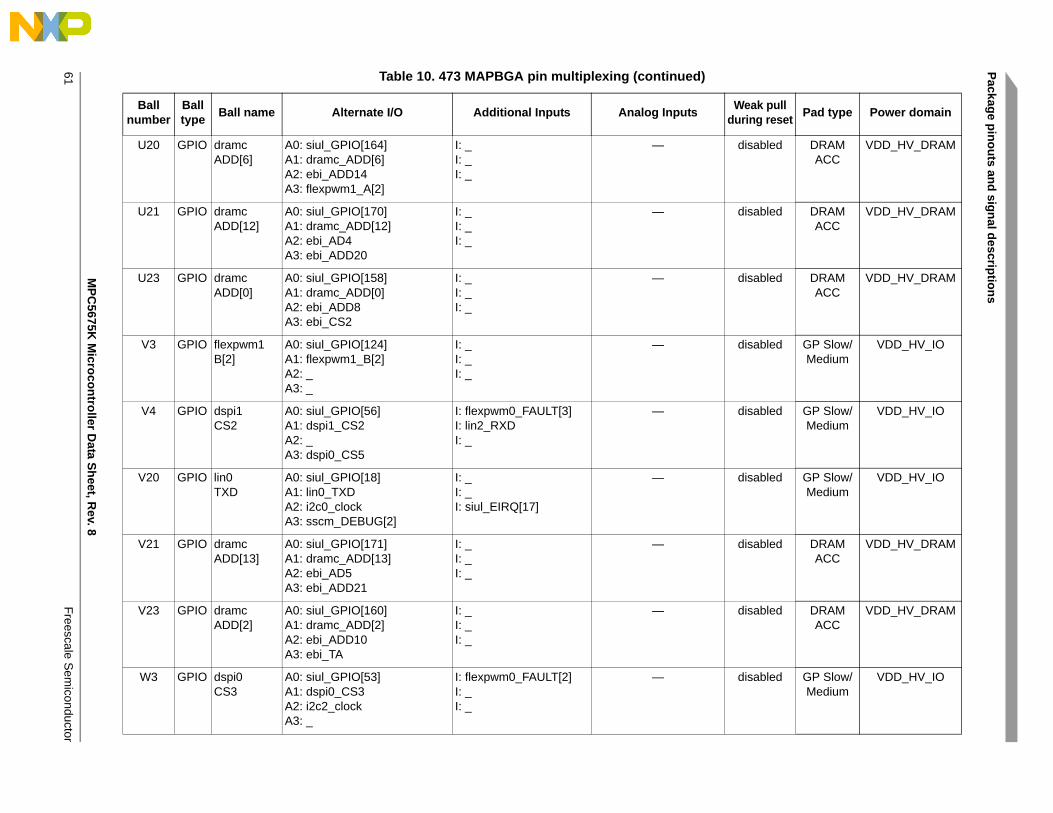
MP
C5
675K M
icroco
ntro
ller Da
ta S
heet, R
ev. 8
Pack
age
pin
ou
ts and
sign
al des
criptio
ns
Fre
escale S
emico
nductor61
U20 GPIO dramcADD[6]
A0: siul_GPIO[164]A1: dramc_ADD[6]A2: ebi_ADD14A3: flexpwm1_A[2]
I: _I: _I: _
— disabled DRAM ACC
VDD_HV_DRAM
U21 GPIO dramcADD[12]
A0: siul_GPIO[170]A1: dramc_ADD[12]A2: ebi_AD4A3: ebi_ADD20
I: _I: _I: _
— disabled DRAM ACC
VDD_HV_DRAM
U23 GPIO dramcADD[0]
A0: siul_GPIO[158]A1: dramc_ADD[0]A2: ebi_ADD8A3: ebi_CS2
I: _I: _I: _
— disabled DRAM ACC
VDD_HV_DRAM
V3 GPIO flexpwm1B[2]
A0: siul_GPIO[124]A1: flexpwm1_B[2]A2: _A3: _
I: _I: _I: _
— disabled GP Slow/Medium
VDD_HV_IO
V4 GPIO dspi1CS2
A0: siul_GPIO[56]A1: dspi1_CS2A2: _A3: dspi0_CS5
I: flexpwm0_FAULT[3]I: lin2_RXDI: _
— disabled GP Slow/Medium
VDD_HV_IO
V20 GPIO lin0TXD
A0: siul_GPIO[18]A1: lin0_TXDA2: i2c0_clockA3: sscm_DEBUG[2]
I: _I: _I: siul_EIRQ[17]
— disabled GP Slow/Medium
VDD_HV_IO
V21 GPIO dramcADD[13]
A0: siul_GPIO[171]A1: dramc_ADD[13]A2: ebi_AD5A3: ebi_ADD21
I: _I: _I: _
— disabled DRAM ACC
VDD_HV_DRAM
V23 GPIO dramcADD[2]
A0: siul_GPIO[160]A1: dramc_ADD[2]A2: ebi_ADD10A3: ebi_TA
I: _I: _I: _
— disabled DRAM ACC
VDD_HV_DRAM
W3 GPIO dspi0CS3
A0: siul_GPIO[53]A1: dspi0_CS3A2: i2c2_clockA3: _
I: flexpwm0_FAULT[2]I: _I: _
— disabled GP Slow/Medium
VDD_HV_IO
Table 10. 473 MAPBGA pin multiplexing (continued)
Ballnumber
Balltype
Ball name Alternate I/O Additional Inputs Analog InputsWeak pull
during resetPad type Power domain

Pack
age
pin
ou
ts and
sign
al des
criptio
ns
MP
C5
675K M
icroco
ntro
ller Da
ta S
heet, R
ev. 8
Fre
escale Se
micondu
ctor
62
W20 GPIO lin0RXD
A0: siul_GPIO[19]A1: _A2: i2c0_dataA3: sscm_DEBUG[3]
I: lin0_RXDI: _I: _
— disabled GP Slow/Medium
VDD_HV_IO
W21 GPIO dramcADD[14]
A0: siul_GPIO[172]A1: dramc_ADD[14]A2: ebi_AD6A3: ebi_ADD22
I: _I: _I: _
— disabled DRAM ACC
VDD_HV_DRAM
W22 GPIO dramcADD[7]
A0: siul_GPIO[165]A1: dramc_ADD[7]A2: ebi_ADD15A3: flexpwm1_B[2]
I: _I: _I: _
— disabled DRAM ACC
VDD_HV_DRAM
W23 GPIO dramcADD[4]
A0: siul_GPIO[162]A1: dramc_ADD[4]A2: ebi_ADD12A3: ebi_ALE
I: _I: _I: _
— disabled DRAM ACC
VDD_HV_DRAM
Y3 GPIO dspi0CS2
A0: siul_GPIO[54]A1: dspi0_CS2A2: i2c2_dataA3: _
I: flexpwm0_FAULT[1]I: _I: _
— disabled GP Slow/Medium
VDD_HV_IO
Y5 GPIO flexpwm1X[0]
A0: siul_GPIO[116]A1: flexpwm1_X[0]A2: etimer2_ETC[0]A3: dspi0_CS1
I: ctu0_EXT_INI: ctu1_EXT_INI: _
— disabled GP Slow/Medium
VDD_HV_IO
Y6 ANA adc3AN[0]
— siul_GPI[229] AN: adc3_AN[0] — Analog VDD_HV_ADR23
Y7 ANA adc2_adc3AN[11]
— siul_GPI[225] AN: adc2_adc3_AN[11] — Analog Shared
VDD_HV_ADR23
Y8 ANA adc2_adc3AN[14]
— siul_GPI[228] AN: adc2_adc3_AN[14] — Analog Shared
VDD_HV_ADR23
Table 10. 473 MAPBGA pin multiplexing (continued)
Ballnumber
Balltype
Ball name Alternate I/O Additional Inputs Analog InputsWeak pull
during resetPad type Power domain
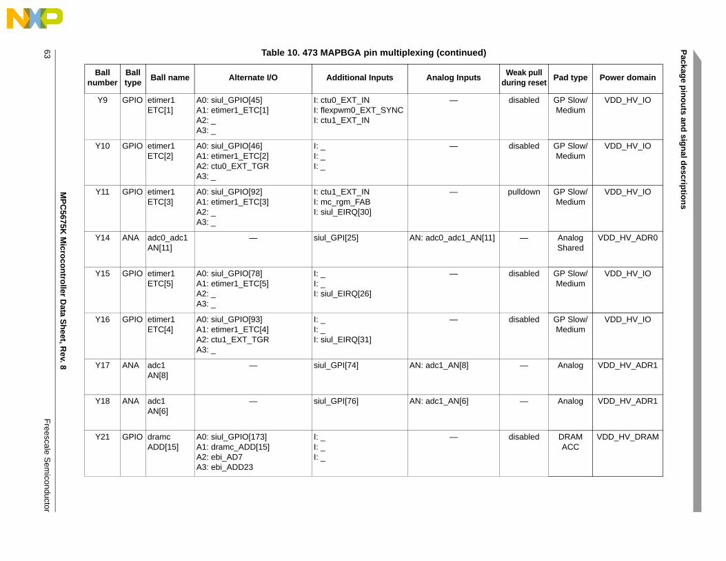
MP
C5
675K M
icroco
ntro
ller Da
ta S
heet, R
ev. 8
Pack
age
pin
ou
ts and
sign
al des
criptio
ns
Fre
escale S
emico
nductor63
Y9 GPIO etimer1ETC[1]
A0: siul_GPIO[45]A1: etimer1_ETC[1]A2: _A3: _
I: ctu0_EXT_INI: flexpwm0_EXT_SYNCI: ctu1_EXT_IN
— disabled GP Slow/Medium
VDD_HV_IO
Y10 GPIO etimer1ETC[2]
A0: siul_GPIO[46]A1: etimer1_ETC[2]A2: ctu0_EXT_TGRA3: _
I: _I: _I: _
— disabled GP Slow/Medium
VDD_HV_IO
Y11 GPIO etimer1ETC[3]
A0: siul_GPIO[92]A1: etimer1_ETC[3]A2: _A3: _
I: ctu1_EXT_INI: mc_rgm_FABI: siul_EIRQ[30]
— pulldown GP Slow/Medium
VDD_HV_IO
Y14 ANA adc0_adc1AN[11]
— siul_GPI[25] AN: adc0_adc1_AN[11] — Analog Shared
VDD_HV_ADR0
Y15 GPIO etimer1ETC[5]
A0: siul_GPIO[78]A1: etimer1_ETC[5]A2: _A3: _
I: _I: _I: siul_EIRQ[26]
— disabled GP Slow/Medium
VDD_HV_IO
Y16 GPIO etimer1ETC[4]
A0: siul_GPIO[93]A1: etimer1_ETC[4]A2: ctu1_EXT_TGRA3: _
I: _I: _I: siul_EIRQ[31]
— disabled GP Slow/Medium
VDD_HV_IO
Y17 ANA adc1AN[8]
— siul_GPI[74] AN: adc1_AN[8] — Analog VDD_HV_ADR1
Y18 ANA adc1AN[6]
— siul_GPI[76] AN: adc1_AN[6] — Analog VDD_HV_ADR1
Y21 GPIO dramcADD[15]
A0: siul_GPIO[173]A1: dramc_ADD[15]A2: ebi_AD7A3: ebi_ADD23
I: _I: _I: _
— disabled DRAM ACC
VDD_HV_DRAM
Table 10. 473 MAPBGA pin multiplexing (continued)
Ballnumber
Balltype
Ball name Alternate I/O Additional Inputs Analog InputsWeak pull
during resetPad type Power domain

Pack
age
pin
ou
ts and
sign
al des
criptio
ns
MP
C5
675K M
icroco
ntro
ller Da
ta S
heet, R
ev. 8
Fre
escale Se
micondu
ctor
64
Y22 GPIO dramcADD[11]
A0: siul_GPIO[169]A1: dramc_ADD[11]A2: ebi_AD3A3: ebi_ADD19
I: _I: _I: _
— disabled DRAM ACC
VDD_HV_DRAM
Y23 GPIO dramcADD[5]
A0: siul_GPIO[163]A1: dramc_ADD[5]A2: ebi_ADD13A3: flexpwm1_B[1]
I: _I: _I: _
— disabled DRAM ACC
VDD_HV_DRAM
AA4 GPIO dspi1CS3
A0: siul_GPIO[55]A1: dspi1_CS3A2: lin2_TXDA3: dspi0_CS4
I: _I: _I: _
— disabled GP Slow/Medium
VDD_HV_IO
AA5 GPIO flexpwm1X[1]
A0: siul_GPIO[119]A1: flexpwm1_X[1]A2: etimer2_ETC[1]A3: dspi0_CS4
I: _I: _I: _
— disabled GP Slow/Medium
VDD_HV_IO
AA6 ANA adc3AN[1]
— siul_GPI[230] AN: adc3_AN[1] — Analog VDD_HV_ADR23
AA7 ANA adc2_adc3AN[12]
— siul_GPI[226] AN: adc2_adc3_AN[12] — Analog Shared
VDD_HV_ADR23
AA8 ANA adc2AN[0]
— siul_GPI[221] AN: adc2_AN[0] — Analog VDD_HV_ADR23
AA11 ANA adc0AN[2]
— siul_GPI[33] AN: adc0_AN[2] — Analog VDD_HV_ADR0
AA12 ANA adc0AN[5]
— siul_GPI[66] AN: adc0_AN[5] — Analog VDD_HV_ADR0
AA13 ANA adc0AN[8]
— siul_GPI[69] AN: adc0_AN[8] — Analog VDD_HV_ADR0
Table 10. 473 MAPBGA pin multiplexing (continued)
Ballnumber
Balltype
Ball name Alternate I/O Additional Inputs Analog InputsWeak pull
during resetPad type Power domain
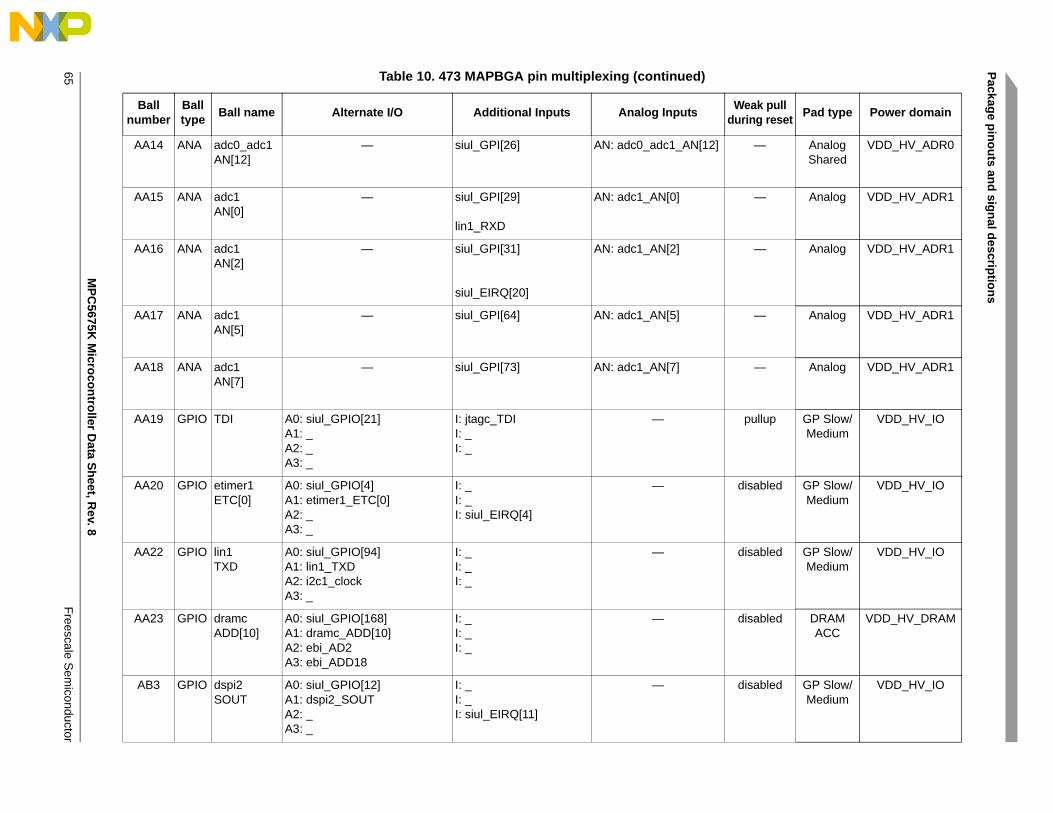
MP
C5
675K M
icroco
ntro
ller Da
ta S
heet, R
ev. 8
Pack
age
pin
ou
ts and
sign
al des
criptio
ns
Fre
escale S
emico
nductor65
AA14 ANA adc0_adc1AN[12]
— siul_GPI[26] AN: adc0_adc1_AN[12] — Analog Shared
VDD_HV_ADR0
AA15 ANA adc1AN[0]
— siul_GPI[29]
lin1_RXD
AN: adc1_AN[0] — Analog VDD_HV_ADR1
AA16 ANA adc1AN[2]
— siul_GPI[31]
siul_EIRQ[20]
AN: adc1_AN[2] — Analog VDD_HV_ADR1
AA17 ANA adc1AN[5]
— siul_GPI[64] AN: adc1_AN[5] — Analog VDD_HV_ADR1
AA18 ANA adc1AN[7]
— siul_GPI[73] AN: adc1_AN[7] — Analog VDD_HV_ADR1
AA19 GPIO TDI A0: siul_GPIO[21]A1: _A2: _A3: _
I: jtagc_TDII: _I: _
— pullup GP Slow/Medium
VDD_HV_IO
AA20 GPIO etimer1ETC[0]
A0: siul_GPIO[4]A1: etimer1_ETC[0]A2: _A3: _
I: _I: _I: siul_EIRQ[4]
— disabled GP Slow/Medium
VDD_HV_IO
AA22 GPIO lin1TXD
A0: siul_GPIO[94]A1: lin1_TXDA2: i2c1_clockA3: _
I: _I: _I: _
— disabled GP Slow/Medium
VDD_HV_IO
AA23 GPIO dramcADD[10]
A0: siul_GPIO[168]A1: dramc_ADD[10]A2: ebi_AD2A3: ebi_ADD18
I: _I: _I: _
— disabled DRAM ACC
VDD_HV_DRAM
AB3 GPIO dspi2SOUT
A0: siul_GPIO[12]A1: dspi2_SOUTA2: _A3: _
I: _I: _I: siul_EIRQ[11]
— disabled GP Slow/Medium
VDD_HV_IO
Table 10. 473 MAPBGA pin multiplexing (continued)
Ballnumber
Balltype
Ball name Alternate I/O Additional Inputs Analog InputsWeak pull
during resetPad type Power domain

Pack
age
pin
ou
ts and
sign
al des
criptio
ns
MP
C5
675K M
icroco
ntro
ller Da
ta S
heet, R
ev. 8
Fre
escale Se
micondu
ctor
66
AB4 GPIO flexpwm1X[2]
A0: siul_GPIO[122]A1: flexpwm1_X[2]A2: etimer2_ETC[2]A3: dspi0_CS5
I: _I: _I: _
— disabled GP Slow/Medium
VDD_HV_IO
AB5 GPIO flexpwm1X[3]
A0: siul_GPIO[125]A1: flexpwm1_X[3]A2: etimer2_ETC[3]A3: dspi0_CS6
I: _I: _I: _
— disabled GP Slow/Medium
VDD_HV_IO
AB6 ANA adc3AN[2]
— siul_GPI[231] AN: adc3_AN[2] — Analog VDD_HV_ADR23
AB7 ANA adc2_adc3AN[13]
— siul_GPI[227] AN: adc2_adc3_AN[13] — Analog Shared
VDD_HV_ADR23
AB8 ANA adc2AN[1]
— siul_GPI[222] AN: adc2_AN[1] — Analog VDD_HV_ADR23
AB9 ANA adc2AN[2]
— siul_GPI[223] AN: adc2_AN[2] — Analog VDD_HV_ADR23
AB10 ANA adc0AN[0]
— siul_GPI[23]
lin0_RXD
AN: adc0_AN[0] — Analog VDD_HV_ADR0
AB11 ANA adc0AN[4]
— siul_GPI[70] AN: adc0_AN[4] — Analog VDD_HV_ADR0
AB12 ANA adc0AN[6]
— siul_GPI[71] AN: adc0_AN[6] — Analog VDD_HV_ADR0
AB13 ANA adc0AN[7]
— siul_GPI[68] AN: adc0_AN[7] — Analog VDD_HV_ADR0
AB14 ANA adc0_adc1AN[13]
— siul_GPI[27] AN: adc0_adc1_AN[13] — Analog Shared
VDD_HV_ADR0
Table 10. 473 MAPBGA pin multiplexing (continued)
Ballnumber
Balltype
Ball name Alternate I/O Additional Inputs Analog InputsWeak pull
during resetPad type Power domain
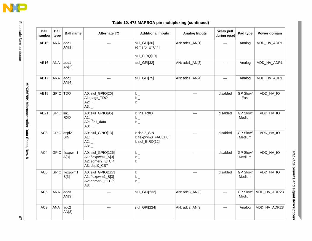
Pack
age
pin
ou
ts and
sign
al des
criptio
ns
MP
C5
675K M
icroco
ntro
ller Da
ta S
heet, R
ev. 8
Fre
escale Se
micondu
ctor
67
AB15 ANA adc1AN[1]
— siul_GPI[30]etimer0_ETC[4]
siul_EIRQ[19]
AN: adc1_AN[1] — Analog VDD_HV_ADR1
AB16 ANA adc1AN[3]
— siul_GPI[32] AN: adc1_AN[3] — Analog VDD_HV_ADR1
AB17 ANA adc1AN[4]
— siul_GPI[75] AN: adc1_AN[4] — Analog VDD_HV_ADR1
AB18 GPIO TDO A0: siul_GPIO[20]A1: jtagc_TDOA2: _A3: _
I: _I: _I: _
— disabled GP Slow/Fast
VDD_HV_IO
AB21 GPIO lin1RXD
A0: siul_GPIO[95]A1: _A2: i2c1_dataA3: _
I: lin1_RXDI: _I: _
— disabled GP Slow/Medium
VDD_HV_IO
AC3 GPIO dspi2SIN
A0: siul_GPIO[13]A1: _A2: _A3: _
I: dspi2_SINI: flexpwm0_FAULT[0]I: siul_EIRQ[12]
— disabled GP Slow/Medium
VDD_HV_IO
AC4 GPIO flexpwm1A[3]
A0: siul_GPIO[126]A1: flexpwm1_A[3]A2: etimer2_ETC[4]A3: dspi0_CS7
I: _I: _I: _
— disabled GP Slow/Medium
VDD_HV_IO
AC5 GPIO flexpwm1B[3]
A0: siul_GPIO[127]A1: flexpwm1_B[3]A2: etimer2_ETC[5]A3: _
I: _I: _I: _
— disabled GP Slow/Medium
VDD_HV_IO
AC6 ANA adc3AN[3]
— siul_GPI[232] AN: adc3_AN[3] — GP Slow/Medium
VDD_HV_ADR23
AC9 ANA adc2AN[3]
— siul_GPI[224] AN: adc2_AN[3] — Analog VDD_HV_ADR23
Table 10. 473 MAPBGA pin multiplexing (continued)
Ballnumber
Balltype
Ball name Alternate I/O Additional Inputs Analog InputsWeak pull
during resetPad type Power domain

MP
C5
675K M
icroco
ntro
ller Da
ta S
heet, R
ev. 8
Pack
age
pin
ou
ts and
sign
al des
criptio
ns
Fre
escale S
emico
nductor68
AC10 ANA adc0AN[1]
— siul_GPI[24]etimer0_ETC[5]
AN: adc0_AN[1] — Analog VDD_HV_ADR0
AC11 ANA adc0AN[3]
— siul_GPI[34] AN: adc0_AN[3] — Analog VDD_HV_ADR0
AC14 ANA adc0_adc1AN[14]
— siul_GPI[28] AN: adc0_adc1_AN[14] — Analog Shared
VDD_HV_ADR0
END OF 473 MAPBGA PIN MULTIPLEXING TABLE
1 Do not connect pin directly to a power supply or ground.
Table 10. 473 MAPBGA pin multiplexing (continued)
Ballnumber
Balltype
Ball name Alternate I/O Additional Inputs Analog InputsWeak pull
during resetPad type Power domain
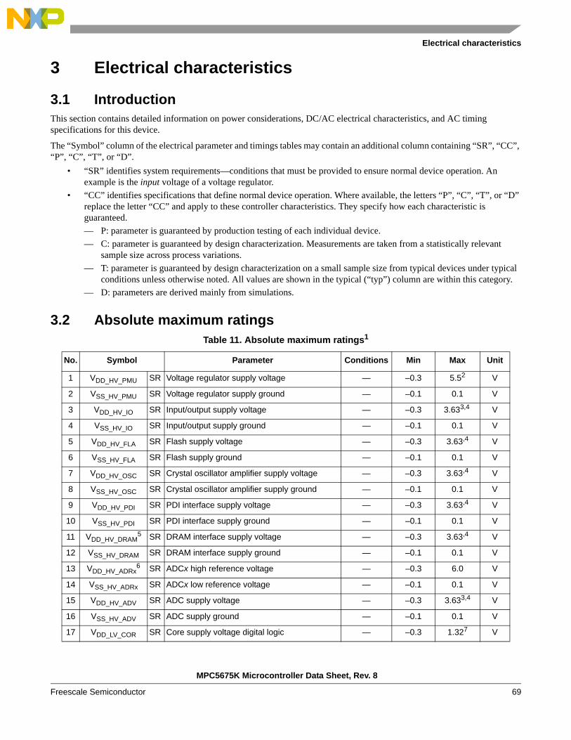
Electrical characteristics
MPC5675K Microcontroller Data Sheet, Rev. 8
Freescale Semiconductor 69
3 Electrical characteristics
3.1 IntroductionThis section contains detailed information on power considerations, DC/AC electrical characteristics, and AC timing specifications for this device.
The “Symbol” column of the electrical parameter and timings tables may contain an additional column containing “SR”, “CC”, “P”, “C”, “T”, or “D”.
• “SR” identifies system requirements—conditions that must be provided to ensure normal device operation. An example is the input voltage of a voltage regulator.
• “CC” identifies specifications that define normal device operation. Where available, the letters “P”, “C”, “T”, or “D” replace the letter “CC” and apply to these controller characteristics. They specify how each characteristic is guaranteed.
— P: parameter is guaranteed by production testing of each individual device.
— C: parameter is guaranteed by design characterization. Measurements are taken from a statistically relevant sample size across process variations.
— T: parameter is guaranteed by design characterization on a small sample size from typical devices under typical conditions unless otherwise noted. All values are shown in the typical (“typ”) column are within this category.
— D: parameters are derived mainly from simulations.
3.2 Absolute maximum ratingsTable 11. Absolute maximum ratings1
No. Symbol Parameter Conditions Min Max Unit
1 VDD_HV_PMU SR Voltage regulator supply voltage — –0.3 5.52 V
2 VSS_HV_PMU SR Voltage regulator supply ground — –0.1 0.1 V
3 VDD_HV_IO SR Input/output supply voltage — –0.3 3.633,4 V
4 VSS_HV_IO SR Input/output supply ground — –0.1 0.1 V
5 VDD_HV_FLA SR Flash supply voltage — –0.3 3.63,4 V
6 VSS_HV_FLA SR Flash supply ground — –0.1 0.1 V
7 VDD_HV_OSC SR Crystal oscillator amplifier supply voltage — –0.3 3.63,4 V
8 VSS_HV_OSC SR Crystal oscillator amplifier supply ground — –0.1 0.1 V
9 VDD_HV_PDI SR PDI interface supply voltage — –0.3 3.63,4 V
10 VSS_HV_PDI SR PDI interface supply ground — –0.1 0.1 V
11 VDD_HV_DRAM5 SR DRAM interface supply voltage — –0.3 3.63,4 V
12 VSS_HV_DRAM SR DRAM interface supply ground — –0.1 0.1 V
13 VDD_HV_ADRx6 SR ADCx high reference voltage — –0.3 6.0 V
14 VSS_HV_ADRx SR ADCx low reference voltage — –0.1 0.1 V
15 VDD_HV_ADV SR ADC supply voltage — –0.3 3.633,4 V
16 VSS_HV_ADV SR ADC supply ground — –0.1 0.1 V
17 VDD_LV_COR SR Core supply voltage digital logic — –0.3 1.327 V

MPC5675K Microcontroller Data Sheet, Rev. 8
Electrical characteristics
Freescale Semiconductor70
3.3 Recommended operating conditions
18 VSS_LV_COR SR Core supply voltage ground digital logic — –0.1 0.1 V
19 VDD_LV_PLL SR PLL supply voltage — –0.3 1.32 V
20 VSS_LV_PLL SR PLL reference voltage — –0.1 0.1 V
21 TVDD SR Slope characteristics on all VDD during power up
— — 25 mV/µs
22 VIN SR Voltage on any pin with respect to its supply rail VDD_HV_xxx
Relative to VDD_HV_xxx
–0.3 VDD_HV_xxx+ 0.38
V
23 IINJPAD SR Injected input current on any pin during overload condition
— –10 10 mA
24 IINJPADA SR Injected input current on any analog pin during overload condition
— –3 3 mA
25 IINJSUM SR Absolute sum of all injected input currents during overload condition
— –50 50 mA
26 TSTG SR Storage temperature — –559 150 °C
27 TSDR SR Maximum Solder Temperature10
Pb-free packageSnPb package
———
260245
°C
28 MSL SR Moisture Sensitivity Level11 — — 3 —
1 Functional operating conditions are given in the DC electrical characteristics. Absolute maximum ratings are stress ratings only, and functional operation at the maxima is not guaranteed. Stress beyond the listed maxima may affect device reliability or cause permanent damage to the device.
2 6.5 V for 10 hours cumulative time, 5.0 V + 10% for time remaining.3 5.3 V for 10 hours cumulative over lifetime of device, 3.63 V for time remaining. 4 Voltage overshoots during a high-to-low or low-to-high transition must not exceed 10 seconds per instance. 5 As the VDD_HV_DRAM_VREF supply should always be constrained by the VDD_HV_DRAM supply for example through a
voltage divider network per the JEDEC specification, the maximum ratings for the VDD_HV_DRAM supply should be used for the VDD_HV_DRAM_VREF reference as well.
6 All VDD_HV_ADRx rails must be operated at the same supply voltage.7 2.0 V for 10 hours cumulative time, 1.2 V + 10% for time remaining. 8 Only when VDD_HV_xxx < 5.2 V. 9 If the ambient temperature is at or above the minimum storage temperature and below the recommended minimum
operating temperature, power may be applied to the device safely. However, functionality is not guaranteed and a power cycle must be administered if in internal regulation mode or an assertion of RESET_SUP_B must be administered if in external regulation mode once device enters into the recommended operating temperature range.
10 Solder profile per CDF-AEC-Q100.11 Moisture sensitivity per JEDEC test method A112.
Table 12. Recommended operating conditions
No. Symbol Parameter Conditions Min Max Unit
1 VDD_HV_PMU SR Voltage regulator supply voltage — 3.0 5.5 V
Table 11. Absolute maximum ratings1 (continued)
No. Symbol Parameter Conditions Min Max Unit
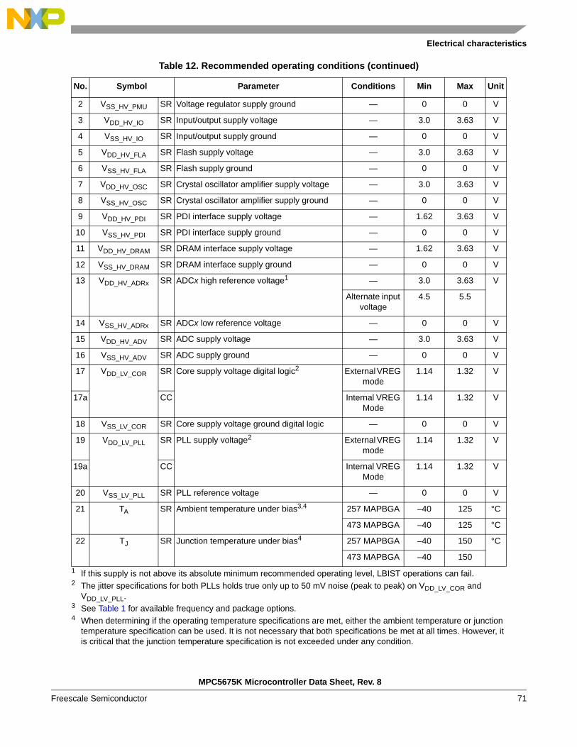
Electrical characteristics
MPC5675K Microcontroller Data Sheet, Rev. 8
Freescale Semiconductor 71
2 VSS_HV_PMU SR Voltage regulator supply ground — 0 0 V
3 VDD_HV_IO SR Input/output supply voltage — 3.0 3.63 V
4 VSS_HV_IO SR Input/output supply ground — 0 0 V
5 VDD_HV_FLA SR Flash supply voltage — 3.0 3.63 V
6 VSS_HV_FLA SR Flash supply ground — 0 0 V
7 VDD_HV_OSC SR Crystal oscillator amplifier supply voltage — 3.0 3.63 V
8 VSS_HV_OSC SR Crystal oscillator amplifier supply ground — 0 0 V
9 VDD_HV_PDI SR PDI interface supply voltage — 1.62 3.63 V
10 VSS_HV_PDI SR PDI interface supply ground — 0 0 V
11 VDD_HV_DRAM SR DRAM interface supply voltage — 1.62 3.63 V
12 VSS_HV_DRAM SR DRAM interface supply ground — 0 0 V
13 VDD_HV_ADRx SR ADCx high reference voltage1 — 3.0 3.63 V
Alternate input voltage
4.5 5.5
14 VSS_HV_ADRx SR ADCx low reference voltage — 0 0 V
15 VDD_HV_ADV SR ADC supply voltage — 3.0 3.63 V
16 VSS_HV_ADV SR ADC supply ground — 0 0 V
17 VDD_LV_COR SR Core supply voltage digital logic2 External VREG mode
1.14 1.32 V
17a CC Internal VREG Mode
1.14 1.32 V
18 VSS_LV_COR SR Core supply voltage ground digital logic — 0 0 V
19 VDD_LV_PLL SR PLL supply voltage2 External VREG mode
1.14 1.32 V
19a CC Internal VREG Mode
1.14 1.32 V
20 VSS_LV_PLL SR PLL reference voltage — 0 0 V
21 TA SR Ambient temperature under bias3,4 257 MAPBGA –40 125 °C
473 MAPBGA –40 125 °C
22 TJ SR Junction temperature under bias4 257 MAPBGA –40 150 °C
473 MAPBGA –40 150
1 If this supply is not above its absolute minimum recommended operating level, LBIST operations can fail.2 The jitter specifications for both PLLs holds true only up to 50 mV noise (peak to peak) on VDD_LV_COR and
VDD_LV_PLL.3 See Table 1 for available frequency and package options. 4 When determining if the operating temperature specifications are met, either the ambient temperature or junction
temperature specification can be used. It is not necessary that both specifications be met at all times. However, it is critical that the junction temperature specification is not exceeded under any condition.
Table 12. Recommended operating conditions (continued)
No. Symbol Parameter Conditions Min Max Unit
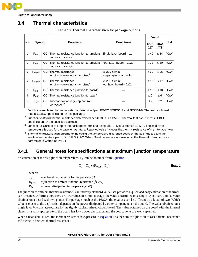
MPC5675K Microcontroller Data Sheet, Rev. 8
Electrical characteristics
Freescale Semiconductor72
3.4 Thermal characteristics
3.4.1 General notes for specifications at maximum junction temperatureAn estimation of the chip junction temperature, TJ, can be obtained from Equation 1:
TJ = TA + (RJA × PD) Eqn. 1
where:
TA = ambient temperature for the package (oC)
RJA = junction to ambient thermal resistance (oC/W)
PD = power dissipation in the package (W)
The junction to ambient thermal resistance is an industry standard value that provides a quick and easy estimation of thermal performance. Unfortunately, there are two values in common usage: the value determined on a single layer board and the value obtained on a board with two planes. For packages such as the PBGA, these values can be different by a factor of two. Which value is closer to the application depends on the power dissipated by other components on the board. The value obtained on a single layer board is appropriate for the tightly packed printed circuit board. The value obtained on the board with the internal planes is usually appropriate if the board has low power dissipation and the components are well separated.
When a heat sink is used, the thermal resistance is expressed in Equation 2 as the sum of a junction to case thermal resistance and a case to ambient thermal resistance:
Table 13. Thermal characteristics for package options
No. Symbol Parameter Conditions
Value
UnitBGA 257
BGA473
1 RJA CC Thermal resistance junction-to-ambient natural convection1
1 Junction-to-Ambient thermal resistance determined per JEDEC JESD51-3 and JESD51-6. Thermal test board meets JEDEC specification for this package.
Single layer board – 1s 40 34 °C/W
2 RJA CC Thermal resistance junction-to-ambient natural convection1
Four layer board – 2s2p 22 20 °C/W
3 RJMA CC Thermal resistance junction-to-moving-air ambient1
@ 200 ft./min., single layer board – 1s
32 26 °C/W
4 RJMA CC Thermal resistance junction-to-moving-air ambient1
@ 200 ft./min., four layer board – 2s2p
18 17 °C/W
5 RJB CC Thermal resistance junction-to-board2
2 Junction-to-Board thermal resistance determined per JEDEC JESD51-8. Thermal test board meets JEDEC specification for the specified package.
— 10 10 °C/W
6 RJC CC Thermal resistance junction-to-case3
3 Junction-to-Case at the top of the package determined using MIL-STD 883 Method 1012.1. The cold plate temperature is used for the case temperature. Reported value includes the thermal resistance of the interface layer.
— 6 6 °C/W
7 JT CC Junction-to-package-top natural convection4
4 Thermal characterization parameter indicating the temperature difference between the package top and the junction temperature per JEDEC JESD51-2. When Greek letters are not available, the thermal characterization parameter is written as Psi-JT.
— 2 2 °C/W

Electrical characteristics
MPC5675K Microcontroller Data Sheet, Rev. 8
Freescale Semiconductor 73
RJA = RJC + RCA Eqn. 2
where:
RJA = junction to ambient thermal resistance (°C/W)
RJC = junction to case thermal resistance (°C/W)
RCA = case to ambient thermal resistance (°C/W)
RJC is device related and cannot be influenced by the user. The user controls the thermal environment to change the case to ambient thermal resistance, RCA. For instance, the user can change the size of the heat sink, the air flow around the device, the interface material, the mounting arrangement on printed circuit board, or change the thermal dissipation on the printed circuit board surrounding the device.
To determine the junction temperature of the device in the application when heat sinks are not used, the Thermal Characterization Parameter (JT) can be used to determine the junction temperature with a measurement of the temperature at the top center of the package case using Equation 3:
TJ = TT + (JT × PD) Eqn. 3
where:
TT = thermocouple temperature on top of the package (°C)
JT = thermal characterization parameter (°C/W)
PD = power dissipation in the package (W)
The thermal characterization parameter is measured per JESD51-2 specification using a 40 gauge type T thermocouple epoxied to the top center of the package case. The thermocouple should be positioned so that the thermocouple junction rests on the package. A small amount of epoxy is placed over the thermocouple junction and over about 1 mm of wire extending from the junction. The thermocouple wire is placed flat against the package case to avoid measurement errors caused by cooling effects of the thermocouple wire.
See [6] to [10] in Section 6, Reference documents, for more information.
3.5 Electromagnetic interference (EMI) characteristics
3.5.1 Test SetupElectromagnetic emission tests are performed by TEM cell [2] and via direct coupling [3] (150 ) measurements.
Electromagnetic immunity is measured by DPI [4].
See Section 6, Reference documents, for more information.
3.5.2 Test parametersThe following test parameters shall be used:
Table 14. EMC test parameters
Method Frequency RangeReceiver
BW Step Size
150 1 MHz to 1000 MHz 1 MHz 500 kHz
TEM

MPC5675K Microcontroller Data Sheet, Rev. 8
Electrical characteristics
Freescale Semiconductor74
In case of only narrow band disturbances the maximum of the results will not change. In case of broadband signals the emission has to be below the limits.
3.6 Electrostatic discharge (ESD) characteristicsElectrostatic discharges (a positive then a negative pulse separated by 1 second) are applied to the pins of each sample according to each pin combination. The sample size depends on the number of supply pins in the device (3 parts × (n + 1) supply pin). This test conforms to the AEC-Q100-002/-003/-011 standard.
3.7 Static latch-up (LU)Two complementary static tests are required on six parts to assess the latch-up performance:
• A supply over voltage is applied to each power supply pin.
• A current injection is applied to each input, output and configurable I/O pin.
These tests are compliant with the EIA/JESD 78 IC latch-up standard.
3.8 Power Management Controller (PMC) electrical characteristics
3.8.1 PMC electrical specificationsThis section contains electrical characteristics for the PMC.
Table 15. ESD ratings1, 2
1 All ESD testing is in conformity with CDF-AEC-Q100 Stress Test Qualification for Automotive Grade Integrated Circuits.
2 A device will be defined as a failure if after exposure to ESD pulses the device no longer meets the device specification requirements. Complete DC parametric and functional testing shall be performed per applicable device specification at room temperature followed by hot temperature, unless specified otherwise in the device specification.
No. Symbol Parameter Conditions Class Max value3
3 Data based on characterization results, not tested in production.
Unit
1 VESD(HBM) SR Electrostatic discharge(Human Body Model)
TA = 25 °Cconforming to AEC-Q100-002
H1C 2000 V
2 VESD(MM) SR Electrostatic discharge(Machine Model)
TA = 25 °Cconforming to AEC-Q100-003
M2 200 V
3 VESD(CDM) SR Electrostatic discharge(Charged Device Model)
TA = 25 °Cconforming to AEC-Q100-011
C3A 750 (corners) V
500
Table 16. Latch-up results
No. Symbol Parameter Conditions Class
1 LU CC Static latch-up class TA = 125 °C conforming to JESD 78 II level A

Electrical characteristics
MPC5675K Microcontroller Data Sheet, Rev. 8
Freescale Semiconductor 75
3.8.2 PMC board schematic and componentsFigure 7 shows a sample application for the PMC.
Table 17. PMC electrical specifications
No. Symbol Parameter Min Typ Max Unit
1 VDD_LV_COR CC Nominal VRC regulated 1.2 V outputVDD_LV_CORVrc after reset 1.2V output with DC load
—
1.178
1.24
1.240
—
1.302
V
2 PorC CC POR rising VDD 1.2 V • POR VDD variation • POR 1.2 V hysteresis
—PorC – 30%
—
0.7PorC
75
—PorC + 30%
—
VV
mV
3 LvdC CC Nominal LVD 1.2 V • LVD rising supply 1.2V after reset • LVD rising supply 1.2V at reset • LVD falling supply 1.2V after reset • LVD falling supply 1.2V at reset
—1.1251.171.1101.155
1.161.16
1.2151.1451.2
—1.1951.261.181.245
VVVVV
4 HvdC CC Nominal HVD 1.2 V • HVD rising supply 1.2V after reset • HVD rising supply 1.2V at reset • HVD falling supply 1.2V after reset • HVD falling supply 1.2V at reset
—1.321.381.291.35
1.361.361.441.331.41
—1.41.5
1.371.47
VVVV
5 PorReg CC POR rising on VDDREG • POR VDDREG variation • POR VDDREG hysteresis
—PorReg – 30%
—
2.00 PorReg
250
—PorReg + 30%
—
VV
mV
6 LvdReg CC Nominal rising LVD 3.3 V on VDDREG, VDDIO, VDDFLASH, and VDDADC
• LVD 3.3 V rising supply after reset • LVD 3.3 V rising supply at reset • LVD 3.3 V falling supply after reset • LVD 3.3 V falling supply at reset • Minimum slew rate • Maximum slew rate
—2.78
2.7652.75
2.735——
2.8652.8652.8652.8352.835
5025
—2.952.9652.922.935
——
VVVVV
mV/msmV/µs
7 LvdStepReg CC Trimming step LVD 3.3 V — 30 — mV
8 Vadctol CC Voltage tolerance of PMC channels1
1 This tolerance can only be achieved when adhering to the PMC internal channel sample time requirements listed in the ADC specifications section.
-20 — +20 mV

MPC5675K Microcontroller Data Sheet, Rev. 8
Electrical characteristics
Freescale Semiconductor76
Figure 7. PMU mandatory external components
3.9 Supply current characteristics
Table 18. VRC SMPS recommended external devices
Referencedesignator
Part description Part type Nominal Description
Ca — capacitor 20 µF, 20 V Filter capacitor
Cb — capacitor 0.1 µF, 20 V Filter capacitor
Cd — capacitor 20 µF, 20 V Supply decoupling cap, ESR < 50 m, as close to PMOS source as possible
Ce — capacitor 0.1 µF, 16 V Ceramic
Cl — capacitor 20 µF, 16 V Buck capacitor, total ESR < 100 m, as close to the coil as possible
D SS8P3L Schottky — Vishay low Vf Schottky diode
L — inductor 4 µH, 1.5 A Buck shielded coil low ESR
Q FDC642P or SQ2301ES or
SI3443DV
pMOS 2 A, 10 V Low threshold PMOS Vth < 1.5 V, [email protected] V < 120 m, Qg < 16 nC
R — resistor 50–100 k Pullup for power PMOS gate
Table 19. Current consumption characteristics1
No. Symbol Parameter Conditions Min Typ Max Unit
1 IDD_LV CC Maximum run IDD(incl. digital core logicand analog block ofthe LV rail)
VDD_LV = 1.36 V, fCore = 180 MHz, 1:2 mode, DPM, both cores executing EMC test code, internal VREG mode, all caches enabled, code execution of core 0 from code flash 0, code execution of core 1 from code flash 1, FMPLL_1 active at 120 MHz.
— 600 900 mA
2 IDD_LV_PLL CC Maximum run IDD for each PLL2
VDD_LV_PLL = 1.36 V, fVCO running at maximum frequency.
— 1.5 2 mA
VDD_HV_PMU
VSS_HV_PMU
VREG_CTRL
VDD_LV_COR
VSS_LV_COR
Ca CbCd
CeCl
L
R
D
Q
Electrical characteristics
MPC5675K Microcontroller Data Sheet, Rev. 8
Freescale Semiconductor 77
3.10 Temperature sensor electrical characteristics
3.11 Main oscillator electrical characteristicsThe MPC5675K provides an oscillator/resonator driver.
3 IDD_HV_FLA3 CC Maximum run IDD
FlashVDD_HV_FLA = 3.6 V, DPM, both cores executing EMC test code, code execution of core 0 from code flash 0, code execution of core 1 from code flash 1.
— 20 30 mA
4 IDD_HV_OSC CC Maximum run IDD OSC
fOSC 4 MHz to 40 MHz,VDD_HV_OSC 3.6 V
— 1 3 mA
5 IDD_HV_ADV CC Maximum run IDD for each ADC4
VDD_HV_ADV = 3.6 V — 2 4 mA
6 IDD_HV_ADR025 CC Maximum reference
IDD6
ADC0 powered on7 — — 2 mA
ADC2 powered on — — 1.2 mA
7 IDD_HV_ADR135 CC Maximum reference
IDD6
ADC1 powered on — — 1.2 mA
ADC3 powered on — — 1.2 mA
8 IDD_HV_ADR08 CC Maximum reference
IDD
ADC0 powered on7 — — 2 mA
9 IDD_HV_ADR18 CC Maximum reference
IDD
ADC1 powered on — — 1.2 mA
10 IDD_HV_ADR238 CC Maximum reference
IDD6
ADC2 powered on — — 1.2 mA
ADC3 powered on — — 1.2 mA
1 Applies to TJ = –40 °C to 150 °C. 2 Total current on IDD_LV_PLL needs to be multiplied with the number of active PLLs. 3 The current specified for Idd_HV_FLA includes current consumed during programming and erase operations.4 Total current on IDD_HV_ADV needs to be multiplied with the number of active ADCs. 5 257 MAPBGA only. 6 Total current on IDD_HV_ADRxx is the sum of both references if both ADCs are powered on. 7 ADC0 includes 0.7 mA dissipation for the temperature sensor (TSENS). 8 473 MAPBGA only.
Table 20. Temperature sensor electrical characteristics
Symbol Parameter Conditions Min Max Unit
1 — P Accuracy TJ = –40 °C to TA = 125 °C –10 10 °C
2 TS D Minimum sampling period — 4 — µs
Table 19. Current consumption characteristics1 (continued)
No. Symbol Parameter Conditions Min Typ Max Unit

MPC5675K Microcontroller Data Sheet, Rev. 8
Electrical characteristics
Freescale Semiconductor78
×
3.12 FMPLL electrical characteristics
Table 21. Main oscillator electrical characteristics
No. Symbol Parameter Conditions1
1 VDD = 3.0 V to 3.6 V, TJ = –40 to 150 °C, unless otherwise specified.
ValueUnit
Min Typ Max
1 FXOSCHS SR Oscillator frequency — 4.0 — 40.0 MHz
2a TXOSCHSSU CC Oscillator start-up time fOSC < 16 MHz — 6 10 ms
2b fOSC = 16 MHz to 40 MHz — 2 4
3 VIH SR Input high level CMOSSchmitt Trigger
Oscillator bypass mode 0.65 × VDD — VDD + 0.4 V
4 VIL SR Input low level CMOSSchmitt Trigger
Oscillator bypass mode –0.4 — 0.35 × VDD V
Table 22. FMPLL electrical characteristics
No. Symbol Parameter Conditions Min Typ Max Unit
1 fREF_CRYSTALfREF_EXT
D FMPLL reference frequency range1, 2
Crystal reference 4 — 120 MHz
2 fPLL_IN D Phase detector input frequency range (after pre-divider)
— 4 — 16 MHz
3 fFMPLLOUT D Clock frequency range in normal mode
See the FMPLL chapter in the chip reference manual for more details on PLL configuration.
16 — 256 MHz
4 fFREE P Free running frequency Measured using clock division (typically 16)
19 — 60 MHz
5 fsys D On-chip FMPLL frequency2 — — — 180 MHz
6 tCYC D System clock period — — — 1 / fsys ns
7a fLORLfLORH
D Loss of reference frequency window3
Lower limit 1.6 — 3.7 MHz
7b Upper limit 24 — 56
8 fSCM D Self-clocked mode frequency4,5 — 20 — 150 MHz
9 tLOCK P Lock time Stable oscillator (fPLLIN = 4 MHz),stable VDD
— — 200 µs
10 tlpll D FMPLL lock time 6, 7 — — — 200 s
11 tdc D Duty cycle of reference — 20 — 80 %
12a CJITTER T CLKOUT period jitter8,9,10,11 Peak-to-peak (clock edge to clock edge), fFMPLLOUT maximum12
— — 160 ps
12b Long-term jitter (avg. over 2 ms interval), fFMPLLOUT maximum
— — 6 ns
13 tPKJIT T Single period jitter (peak to peak)
PHI @ 16 MHz,Input clock @ 4 MHz
— — ±500 ps

Electrical characteristics
MPC5675K Microcontroller Data Sheet, Rev. 8
Freescale Semiconductor 79
3.13 16 MHz RC oscillator electrical characteristics
14 tLTJIT T Long term jitter PHI @ 16 MHz,Input clock @ 4 MHz
— — ±6 ns
15 fLCK D Frequency LOCK range — –4 — +4 % fFMPLLOUT
16 fUL D Frequency un-LOCK range — –16 — +16 % fFMPLLOUT
17a fCSfDS
D Modulation Depth Center spread ±0.25 — ±4 %fFMPLLOUT17b Down Spread –0.5 — –8
18 fMOD D Modulation frequency13 31 < LDF14 < 63LDF > 63
— — (2240/LDF)35
kHz
1 Considering operation with FMPLL not bypassed.2 PFD clock range is 4– 16 MHz. An appropriate PLL Input division factor (IDF) should be chosen to divide the reference
frequency to this range.3 “Loss of Reference Frequency” window is the reference frequency range outside of which the FMPLL is in self clocked mode.4 Self clocked mode frequency is the frequency that the FMPLL operates at when the reference frequency falls outside the fLOR
window.5 fVCO is the frequency at the output of the VCO; its range is 256–512 MHz.
fSCM is the self-clocked mode frequency (free running frequency); its range is 20–150 MHz.fsys = fVCOODF
6 This value is determined by the crystal manufacturer and board design. For 4 MHz to 20 MHz crystals specified for this FMPLL, load capacitors should not exceed these limits.
7 This specification applies to the period required for the FMPLL to relock after changing the MFD frequency control bits in the synthesizer control register (SYNCR).
8 This value is determined by the crystal manufacturer and board design.9 Jitter is the average deviation from the programmed frequency measured over the specified interval at maximum fFMPLLOUT.
Measurements are made with the device powered by filtered supplies and clocked by a stable external clock signal. Noise injected into the FMPLL circuitry via VDDPLL and VSSPLL and variation in crystal oscillator frequency increase the CJITTER percentage for a given interval.
10 Proper PC board layout procedures must be followed to achieve specifications.11 Values are with frequency modulation disabled. If frequency modulation is enabled, jitter is the sum of CJITTER and either fCS
or fDS (depending on whether center spread or down spread modulation is enabled).12 Core operating at 180 MHz.13 Modulation depth is attenuated from depth setting when operating at modulation frequencies above 50 kHz.14 PLL Loop Division Factor (LDF).
Table 23. RC oscillator electrical characteristics
No. Symbol Parameter Conditions Min Typ Max Unit
1 fRC CC RC oscillator frequency 25 °C, 1.2 V trimmed — 16 — MHz
2 RCMVAR CC Frequency spread: The variation in output frequency from PTF1 across temperature and supply voltage range
— — — ±5 %
Table 22. FMPLL electrical characteristics (continued)
No. Symbol Parameter Conditions Min Typ Max Unit
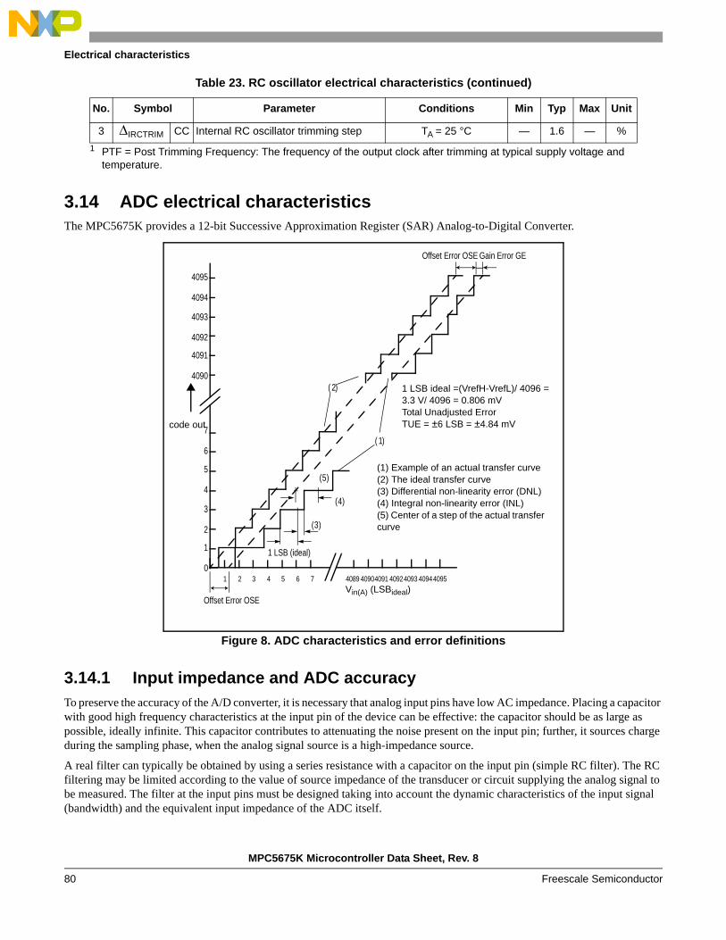
MPC5675K Microcontroller Data Sheet, Rev. 8
Electrical characteristics
Freescale Semiconductor80
3.14 ADC electrical characteristicsThe MPC5675K provides a 12-bit Successive Approximation Register (SAR) Analog-to-Digital Converter.
Figure 8. ADC characteristics and error definitions
3.14.1 Input impedance and ADC accuracyTo preserve the accuracy of the A/D converter, it is necessary that analog input pins have low AC impedance. Placing a capacitor with good high frequency characteristics at the input pin of the device can be effective: the capacitor should be as large as possible, ideally infinite. This capacitor contributes to attenuating the noise present on the input pin; further, it sources charge during the sampling phase, when the analog signal source is a high-impedance source.
A real filter can typically be obtained by using a series resistance with a capacitor on the input pin (simple RC filter). The RC filtering may be limited according to the value of source impedance of the transducer or circuit supplying the analog signal to be measured. The filter at the input pins must be designed taking into account the dynamic characteristics of the input signal (bandwidth) and the equivalent input impedance of the ADC itself.
3 IRCTRIM CC Internal RC oscillator trimming step TA = 25 °C — 1.6 — %
1 PTF = Post Trimming Frequency: The frequency of the output clock after trimming at typical supply voltage and temperature.
Table 23. RC oscillator electrical characteristics (continued)
No. Symbol Parameter Conditions Min Typ Max Unit
( 2)
( 1)
(3)
(4)
(5)
Offset Error OSE
Offset Error OSE
Gain Error GE
1 LSB (ideal)
Vin(A) (LSBideal)
(1) Example of an actual transfer curve(2) The ideal transfer curve(3) Differential non-linearity error (DNL)(4) Integral non-linearity error (INL)(5) Center of a step of the actual transfer curve
code out
4095
4094
4093
4092
4091
4090
5
4
3
2
1
0
7
6
1 2 3 4 5 6 7 4089 40904091 40924093 40944095
1 LSB ideal =(VrefH-VrefL)/ 4096 = 3.3 V/ 4096 = 0.806 mVTotal Unadjusted ErrorTUE = ±6 LSB = ±4.84 mV

Electrical characteristics
MPC5675K Microcontroller Data Sheet, Rev. 8
Freescale Semiconductor 81
In fact a current sink contributor is represented by the charge sharing effects with the sampling capacitance: CS and CP2 being substantially a switched capacitance, with a frequency equal to the conversion rate of the ADC, it can be seen as a resistive path to ground. For instance, assuming a conversion rate of 1 MHz, with CS equal to 3 pF, a resistance of 330 k is obtained (REQ = 1 / (fC CS), where fC represents the conversion rate at the considered channel). To minimize the error induced by the voltage partitioning between this resistance (sampled voltage on CS) and the sum of RS + RF , the external circuit must be designed to respect Equation 4:
Eqn. 4
Equation 4 generates a constraint for external network design, in particular on resistive path. Internal switch resistances (RSW and RAD) can be neglected with respect to external resistances.
Figure 9. Input equivalent circuit
A second aspect involving the capacitance network shall be considered. Assuming the three capacitances CF, CP1, and CP2 are initially charged at the source voltage VA (please see the equivalent circuit in Figure 9): A charge sharing phenomenon is installed when the sampling phase is started (A/D switch is closed).
Figure 10. Transient behavior during sampling phase
In particular two different transient periods can be distinguished:
VA
RS RF+
REQ--------------------- 1
2--- LSB
RF
CF
RS RL RSW1
CP2
VDD
SamplingSource Filter Current Limiter
EXTERNAL CIRCUIT INTERNAL CIRCUIT SCHEME
RS Source ImpedanceRF Filter ResistanceCF Filter CapacitanceRL Current Limiter ResistanceRSW1 Channel Selection Switch ImpedanceRAD Sampling Switch ImpedanceCP Pin Capacitance (two contributions, CP1 and CP2)CS Sampling Capacitance
CP1
RAD
ChannelSelection
VA CS
VA
VA1
VA2
tTS
VCS Voltage Transient on CS
V <0.5 LSB
1 2
1 < (RSW + RAD) CS << TS
2 = RL (CS + CP1 + CP2)
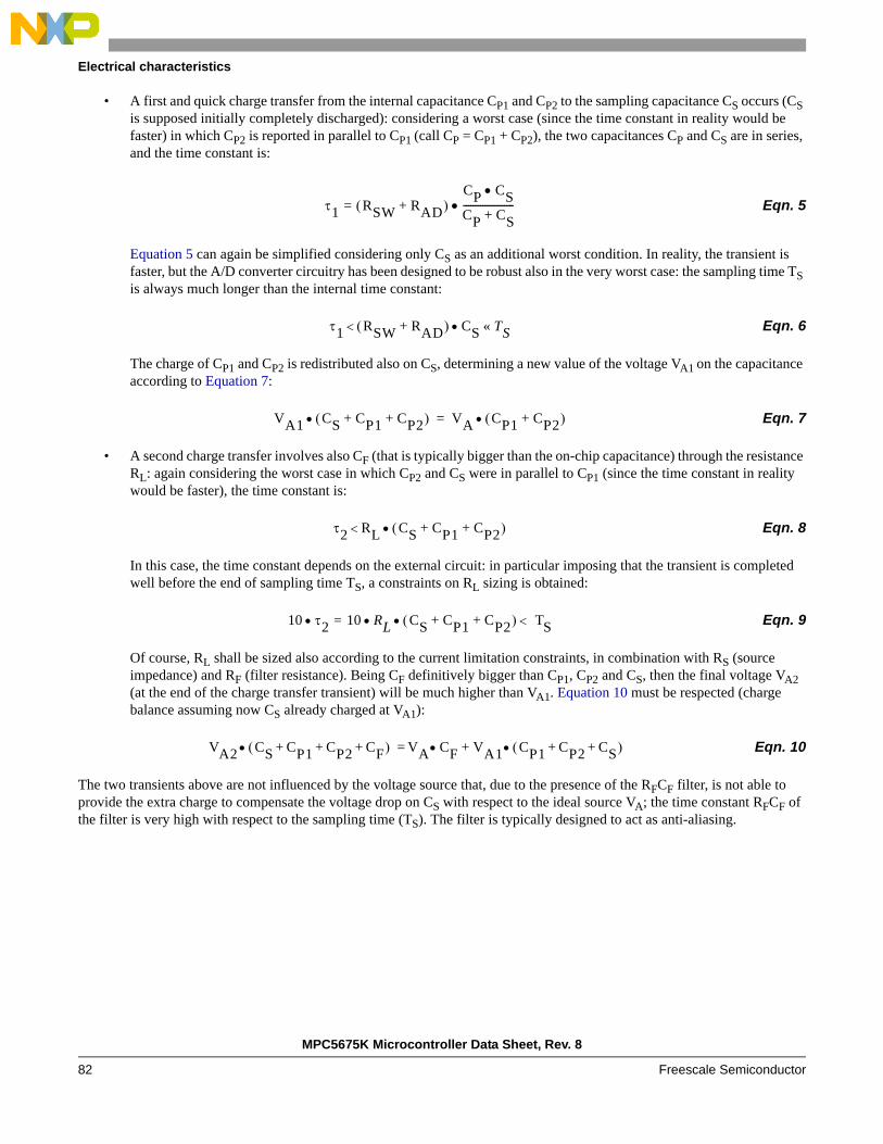
MPC5675K Microcontroller Data Sheet, Rev. 8
Electrical characteristics
Freescale Semiconductor82
• A first and quick charge transfer from the internal capacitance CP1 and CP2 to the sampling capacitance CS occurs (CS is supposed initially completely discharged): considering a worst case (since the time constant in reality would be faster) in which CP2 is reported in parallel to CP1 (call CP = CP1 + CP2), the two capacitances CP and CS are in series, and the time constant is:
Eqn. 5
Equation 5 can again be simplified considering only CS as an additional worst condition. In reality, the transient is faster, but the A/D converter circuitry has been designed to be robust also in the very worst case: the sampling time TS is always much longer than the internal time constant:
Eqn. 6
The charge of CP1 and CP2 is redistributed also on CS, determining a new value of the voltage VA1 on the capacitance according to Equation 7:
Eqn. 7
• A second charge transfer involves also CF (that is typically bigger than the on-chip capacitance) through the resistance RL: again considering the worst case in which CP2 and CS were in parallel to CP1 (since the time constant in reality would be faster), the time constant is:
Eqn. 8
In this case, the time constant depends on the external circuit: in particular imposing that the transient is completed well before the end of sampling time TS, a constraints on RL sizing is obtained:
Eqn. 9
Of course, RL shall be sized also according to the current limitation constraints, in combination with RS (source impedance) and RF (filter resistance). Being CF definitively bigger than CP1, CP2 and CS, then the final voltage VA2 (at the end of the charge transfer transient) will be much higher than VA1. Equation 10 must be respected (charge balance assuming now CS already charged at VA1):
Eqn. 10
The two transients above are not influenced by the voltage source that, due to the presence of the RFCF filter, is not able to provide the extra charge to compensate the voltage drop on CS with respect to the ideal source VA; the time constant RFCF of the filter is very high with respect to the sampling time (TS). The filter is typically designed to act as anti-aliasing.
1 RSW RAD+ =CP CS
CP CS+---------------------
1 RSW RAD+ CS TS«
VA1 CS CP1 CP2+ + VA CP1 CP2+ =
2 RL CS CP1 CP2+ +
10 2 10 RL CS CP1 CP2+ + = TS
VA2 CS CP1 CP2 CF+ + + VA CF VA1+ CP1 CP2+ CS+ =

Electrical characteristics
MPC5675K Microcontroller Data Sheet, Rev. 8
Freescale Semiconductor 83
Figure 11. Spectral representation of input signal
Calling f0 the bandwidth of the source signal (and as a consequence the cut-off frequency of the anti-aliasing filter, fF), according to the Nyquist theorem the conversion rate fC must be at least 2f0; it means that the constant time of the filter is greater than or at least equal to twice the conversion period (TC). Again the conversion period TC is longer than the sampling time TS, which is just a portion of it, even when fixed channel continuous conversion mode is selected (fastest conversion rate at a specific channel): in conclusion it is evident that the time constant of the filter RFCF is definitively much higher than the sampling time TS, so the charge level on CS cannot be modified by the analog signal source during the time in which the sampling switch is closed.
The considerations above lead to impose new constraints on the external circuit, to reduce the accuracy error due to the voltage drop on CS; from the two charge balance equations above, it is simple to derive Equation 11 between the ideal and real sampled voltage on CS:
Eqn. 11
From this formula, in the worst case (when VA is maximum, that is for instance 5 V), assuming to accept a maximum error of half a count, a constraint is evident on CF value:
Eqn. 12
Table 24. ADC conversion characteristics
No. Symbol Parameter Conditions1 Min Typ Max Unit
1 fCK SR ADC clock frequency (depends on ADC configuration)(The duty cycle depends on AD_CK2 frequency)
— 3 — 60 MHz
2 fs SR Sampling frequency — — — 959 kHz
3 tADC_S D Sample time3 60 MHz 383 — — ns
4 tADC_S
_PMC
C Sample time of internal PMC channels. — 717 — — ns
5 tADC_E P Evaluation time4 60 MHz 600 — — ns
f0 f
Analog Source Bandwidth (VA)
f0 f
Sampled Signal Spectrum (fC = conversion Rate)
fCf
Anti-Aliasing Filter (fF = RC Filter pole)
fF
2 f0 fC (Nyquist)
fF f0 (Anti-aliasing Filtering Condition)
TC 2 RFCF (Conversion Rate vs. Filter Pole)
Noise
VA2
VA-----------
CP1 CP2+ CF+
CP1 CP2+ CF CS+ +--------------------------------------------------------=
CF 8192 CS
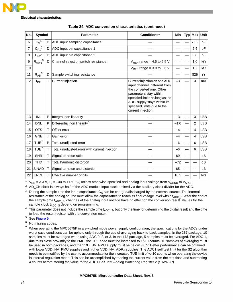
MPC5675K Microcontroller Data Sheet, Rev. 8
Electrical characteristics
Freescale Semiconductor84
6 CS5 D ADC input sampling capacitance — — — 7.32 pF
7 CP15 D ADC input pin capacitance 1 — — — 2.5 pF
8 CP25 D ADC input pin capacitance 2 — — — 0.8 pF
9 RSW15 D Channel selection switch resistance VREF range = 4.5 to 5.5 V — — 1.0 k
10 VREF range = 3.0 to 3.6 V — — 1.2 k
11 RAD5 D Sample switching resistance — — — 825
12 IINJ T Current injection Current injection on one ADC input channel, different from the converted one. Other parameters stay within specified limits as long as the ADC supply stays within its specified limits due to the current injection.
–3 — 3 mA
13 INL P Integral non linearity — –3 — 3 LSB
14 DNL P Differential non linearity6 — –1.0 — 2 LSB
15 OFS T Offset error — –4 — 4 LSB
16 GNE T Gain error — –4 — 4 LSB
17 TUE7 P Total unadjusted error — –6 — 6 LSB
18 TUE7 T Total unadjusted error with current injection — –6 — 6 LSB
19 SNR T Signal-to-noise ratio — 69 — — dB
20 THD T Total harmonic distortion — –72 — — dB
21 SINAD T Signal-to-noise and distortion — 65 — — dB
22 ENOB T Effective number of bits — 10.5 — — bits
1 VDD = 3.3 V, TJ = –40 to +150 °C, unless otherwise specified and analog input voltage from VAGND to VAREF.2 AD_CK clock is always half of the ADC module input clock defined via the auxiliary clock divider for the ADC.3 During the sample time the input capacitance CS can be charged/discharged by the external source. The internal
resistance of the analog source must allow the capacitance to reach its final voltage level within tADC_S. After the end of the sample time tADC_S, changes of the analog input voltage have no effect on the conversion result. Values for the sample clock tADC_S depend on programming.
4 This parameter does not include the sample time tADC_S, but only the time for determining the digital result and the time to load the result register with the conversion result.
5 See Figure 9.6 No missing codes. 7 When operating the MPC5675K in a switched mode power supply configuration, the specifications for the ADCs under
worst case conditions can be upheld only through the use of averaging back-to-back samples. In the 257 package, 10 samples must be averaged when using ADC 0, 2, or 3. In the 473 package, 5 samples must be averaged. For ADC 1, due to its close proximity to the PMC, the TUE spec must be increased to +/-10 counts, 10 samples of averaging must be used in both packages, and the VDD_HV_PMU supply must be below 3.6 V. Better performance can be obtained with lower VDD_HV_PMU supplies and higher VDD_HV_ADRx supplies. The ADC1 self test limit for the S2 algorithm needs to be modified by the user to accommodate for the increased TUE limit of +/-10 counts when operating the device in internal regulation mode. This can be accomplished by reading the current value from the test flash and subtracting 4 counts before storing the value to the ADC1 Self Test Analog Watchdog Register 2 (STAW2R).
Table 24. ADC conversion characteristics (continued)
No. Symbol Parameter Conditions1 Min Typ Max Unit
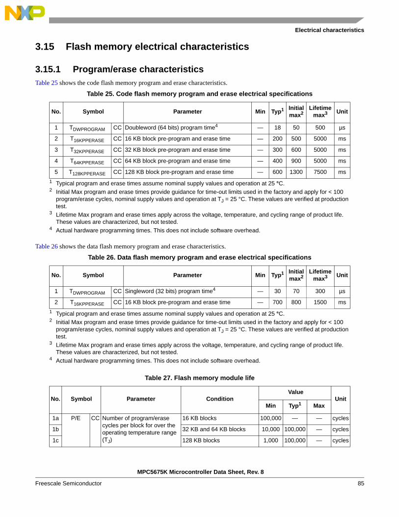
Electrical characteristics
MPC5675K Microcontroller Data Sheet, Rev. 8
Freescale Semiconductor 85
3.15 Flash memory electrical characteristics
3.15.1 Program/erase characteristicsTable 25 shows the code flash memory program and erase characteristics.
Table 26 shows the data flash memory program and erase characteristics.
Table 25. Code flash memory program and erase electrical specifications
No. Symbol Parameter Min Typ1
1 Typical program and erase times assume nominal supply values and operation at 25 °C.
Initialmax2
2 Initial Max program and erase times provide guidance for time-out limits used in the factory and apply for < 100 program/erase cycles, nominal supply values and operation at TJ = 25 °C. These values are verified at production test.
Lifetimemax3
3 Lifetime Max program and erase times apply across the voltage, temperature, and cycling range of product life. These values are characterized, but not tested.
Unit
1 TDWPROGRAM CC Doubleword (64 bits) program time4
4 Actual hardware programming times. This does not include software overhead.
— 18 50 500 µs
2 T16KPPERASE CC 16 KB block pre-program and erase time — 200 500 5000 ms
3 T32KPPERASE CC 32 KB block pre-program and erase time — 300 600 5000 ms
4 T64KPPERASE CC 64 KB block pre-program and erase time — 400 900 5000 ms
5 T128KPPERASE CC 128 KB block pre-program and erase time — 600 1300 7500 ms
Table 26. Data flash memory program and erase electrical specifications
No. Symbol Parameter Min Typ1
1 Typical program and erase times assume nominal supply values and operation at 25 °C.
Initialmax2
2 Initial Max program and erase times provide guidance for time-out limits used in the factory and apply for < 100 program/erase cycles, nominal supply values and operation at TJ = 25 °C. These values are verified at production test.
Lifetimemax3
3 Lifetime Max program and erase times apply across the voltage, temperature, and cycling range of product life. These values are characterized, but not tested.
Unit
1 TDWPROGRAM CC Singleword (32 bits) program time4
4 Actual hardware programming times. This does not include software overhead.
— 30 70 300 µs
2 T16KPPERASE CC 16 KB block pre-program and erase time — 700 800 1500 ms
Table 27. Flash memory module life
No. Symbol Parameter Condition Value
UnitMin Typ1 Max
1a P/E CC Number of program/erase cycles per block for over the operating temperature range (TJ)
16 KB blocks 100,000 — — cycles
1b 32 KB and 64 KB blocks 10,000 100,000 — cycles
1c 128 KB blocks 1,000 100,000 — cycles
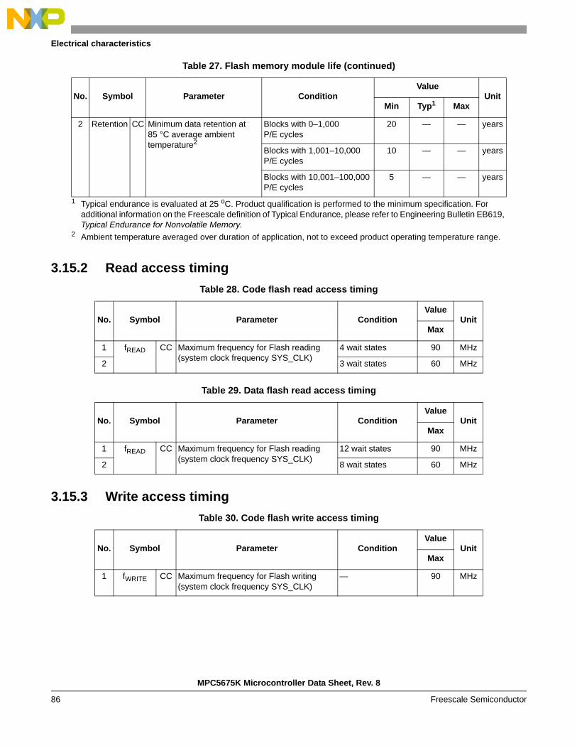
MPC5675K Microcontroller Data Sheet, Rev. 8
Electrical characteristics
Freescale Semiconductor86
3.15.2 Read access timing
3.15.3 Write access timing
2 Retention CC Minimum data retention at 85 °C average ambient temperature2
Blocks with 0–1,000 P/E cycles
20 — — years
Blocks with 1,001–10,000 P/E cycles
10 — — years
Blocks with 10,001–100,000 P/E cycles
5 — — years
1 Typical endurance is evaluated at 25 oC. Product qualification is performed to the minimum specification. For additional information on the Freescale definition of Typical Endurance, please refer to Engineering Bulletin EB619, Typical Endurance for Nonvolatile Memory.
2 Ambient temperature averaged over duration of application, not to exceed product operating temperature range.
Table 28. Code flash read access timing
No. Symbol Parameter ConditionValue
UnitMax
1 fREAD CC Maximum frequency for Flash reading (system clock frequency SYS_CLK)
4 wait states 90 MHz
2 3 wait states 60 MHz
Table 29. Data flash read access timing
No. Symbol Parameter ConditionValue
UnitMax
1 fREAD CC Maximum frequency for Flash reading (system clock frequency SYS_CLK)
12 wait states 90 MHz
2 8 wait states 60 MHz
Table 30. Code flash write access timing
No. Symbol Parameter ConditionValue
UnitMax
1 fWRITE CC Maximum frequency for Flash writing (system clock frequency SYS_CLK)
— 90 MHz
Table 27. Flash memory module life (continued)
No. Symbol Parameter Condition Value
UnitMin Typ1 Max

Electrical characteristics
MPC5675K Microcontroller Data Sheet, Rev. 8
Freescale Semiconductor 87
3.16 SRAM memory electrical characteristics
3.17 GP pads specificationsThis section specifies the electrical characteristics of the GP pads. Please refer to the tables in Section 2.2, Pin descriptions, for a cross reference between package pins and pad types.
3.17.1 GP pads DC specificationsTable 33 gives the DC electrical characteristics at 3.3 V (3.0 V < VDD_HV_IO < 3.6 V).
Table 31. Data flash write access timing
No. Symbol Parameter ConditionValue
UnitMax
1 fWRITE CC Maximum frequency for Flash writing (system clock frequency SYS_CLK)
— 90 MHz
Table 32. System SRAM memory read/write access timing
No. Symbol Parameter ConditionValue
UnitMax
1 sREAD/WRITE CC Maximum frequency for system SRAM reading/writing (system clock frequency SYS_CLK)
1 wait state 90 MHz
Table 33. GP pads DC electrical characteristics1
No. Symbol Parameter Conditions Min Typ Max Unit
1 VIL SR Low level input voltage — –0.12 — 0.35 VDD_HV_IO V
2 VIH SR High level input voltage — 0.65 VDD_HV_IO — VDD_HV_IO + 0.12 V
3 VHYS CC Schmitt trigger hysteresis — 0.1 VDD_HV_IO — — V
4 VOL_S CC Slow, low level output voltage IOL = 1.5 mA — — 0.5 V
5 VOH_S CC Slow, high level output voltage IOH = –1.5 mA VDD_HV_IO – 0.8 — — V
6 VOL_M CC Medium, low level output voltage
IOL = 2 mA — — 0.5 V
7 VOH_M CC Medium, high level output voltage
IOH = –2 mA VDD_HV_IO – 0.8 — — V
8 VOL_F CC Fast, high level output voltage IOL = 11 mA — — 0.5 V
9 VOH_F CC Fast, high level output voltage IOH = –11 mA VDD_HV_IO – 0.8 — — V
10 VOL_SYM CC Symmetric, high level output voltage
IOL = 5 mA — — 0.5 V
11 VOH_SYM CC Symmetric, high level output voltage
IOH = –5 mA VDD_HV_IO – 0.8 — — V

MPC5675K Microcontroller Data Sheet, Rev. 8
Electrical characteristics
Freescale Semiconductor88
3.17.2 GP pads AC specifications
12 IPU CC Equivalent pullup current VIN = VIL –130 — — µA
VIN = VIH — — –10
13 IPD CC Equivalent pulldown current VIN = VIL 10 — — µA
VIN = VIH — — 130
14 IIL P Input leakage current (all bidirectional ports)
TA = –40 to 150 °C
-1 — 1 µA
P Input leakage current (All single ADC channels)3
TA = –40 to 150 °C
-0.25 — 0.25 µA
P Input leakage current (All shared ADC channels)
TA = –40 to 150 °C
-0.3 — 0.3 µA
16 VILR SR RESET, low level input voltage — –0.42 — 0.35 VDD_HV_IO V
17 VIHR SR RESET, high level input voltage — 0.65 VDD_HV_IO — VDD_HV_IO+0.42 V
18 VHYSR CC RESET, Schmitt trigger hysteresis
— 0.1 VDD_HV_IO — — V
19 VOLR CC RESET, low level output voltage IOL = 2 mA — — 0.5 V
20 IPD CC RESET, equivalent pulldown current
VIN = VIL 10 — — µA
VIN = VIH — — 130
21 CIN D Input pad capacitance — — — 3 pF
22 VILRSB SR Reset Sup B, Low level input voltage
— -0.12 — 0.30 VDD_HV_IO
V
23 VIHRSB SR Reset Sup B, High level input voltage
— 0.65 VDD_HV_IO — VDD_HV_IO + 0.12 V
1 The values provided in this table are not applicable for PDI and EBI/DRAM interface. 2 “SR” parameter values must not exceed the absolute maximum ratings shown in Table 11.
3 Specified values are applicable to all modes of the pad, i.e., IBE = 0/1 and/or APC = 0/1.
Table 34. GP pads AC electrical characteristics1
No. Pad
Tswitchon1
(ns)Rise/Fall2
(ns)Frequency
(MHz)Current slew3
(mA/ns) Load drive(pF)
Min Typ Max Min Typ Max Min Typ Max Min Typ Max
1 Slow 3 — 40 4 — 40 — — 4 0.01 — 2 25
3 — 40 6 — 50 — — 2 0.01 — 2 50
3 — 40 10 — 75 — — 2 0.01 — 2 100
3 — 40 14 — 100 — — 2 0.01 — 2 200
Table 33. GP pads DC electrical characteristics1 (continued)
No. Symbol Parameter Conditions Min Typ Max Unit

Electrical characteristics
MPC5675K Microcontroller Data Sheet, Rev. 8
Freescale Semiconductor 89
3.17.3 I/O pad current specificationsThe power consumption of an I/O segment is dependent on the usage of the pins on a particular segment. The power consumption is the sum of all output pin currents for a particular segment. The output pin current can be calculated based on the voltage, frequency, and load on the pin.
3.17.4 Power Sequence Pin States for GPIO Pads
2 Medium 1 — 15 2 — 12 — — 40 2.5 — 7 25
1 — 15 4 — 25 — — 20 2.5 — 7 50
1 — 15 8 — 40 — — 13 2.5 — 7 100
1 — 15 14 — 70 — — 7 2.5 — 7 200
3 Fast 1 — 6 1 — 4 — — 72 3 — 40 25
1 — 6 1.5 — 7 — — 55 7 — 40 50
1 — 6 3 — 12 — — 40 7 — 40 100
1 — 6 5 — 18 — — 25 7 — 40 200
4 Symmetric 1 — 8 1 — 5 — — 50 3 — 25 25
5 Pullup/down(3.6 V max)
— — — — — 7500 — — — — — — 50
1 The values provided in this table are not applicable for PDI and EBI/DRAM interface. 2 Slope at rising/falling edge. 3 Data based on characterization results, not tested in production.
Table 35. I/O pad current specifications
Pad Type Load (pF)
Frequency(MHz)
VDD_HV_IO (V)
Current(mA)
GP Slow/Medium 20 4 3.6 0.30
GP Slow/Symmetric 20 10 3.6 0.76
GP Slow/Fast 20 45 3.6 3.40
GP Slow 20 0.5 3.6 0.04
Table 36. Power sequence pin states for GPIO pads
VDD_LV_COR VDD_HV_IO Pad Function
Low Low Outputs Disabled
Low High Outputs Disabled
High Low Outputs Disabled
Table 34. GP pads AC electrical characteristics1 (continued)
No. Pad
Tswitchon1
(ns)Rise/Fall2
(ns)Frequency
(MHz)Current slew3
(mA/ns) Load drive(pF)
Min Typ Max Min Typ Max Min Typ Max Min Typ Max
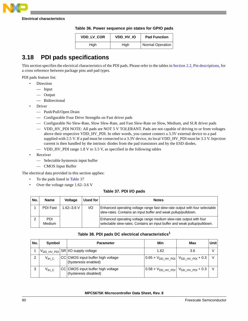
MPC5675K Microcontroller Data Sheet, Rev. 8
Electrical characteristics
Freescale Semiconductor90
3.18 PDI pads specificationsThis section specifies the electrical characteristics of the PDI pads. Please refer to the tables in Section 2.2, Pin descriptions, for a cross reference between package pins and pad types.
PDI pads feature list:
• Direction
— Input
— Output
— Bidirectional
• Driver
— Push/Pull/Open Drain
— Configurable Four Drive Strengths on Fast driver pads
— Configurable No Slew-Rate, Slow Slew-Rate, and Fast Slew-Rate on Slow, Medium, and SLR driver pads
— VDD_HV_PDI NOTE: All pads are NOT 5 V TOLERANT. Pads are not capable of driving to or from voltages above their respective VDD_HV_PDI. In other words, you cannot connect a 3.3V external device to a pad supplied with 2.5 V. If a pad must be connected to a 3.3V device, its local VDD_HV_PDI must be 3.3 V. Injection current is then handled by the intrinsic diodes from the pad transistors and by the ESD diodes.
— VDD_HV_PDI range 1.8 V to 3.3 V, as specified in the following tables
• Receiver
— Selectable hysteresis input buffer
— CMOS Input Buffer
The electrical data provided in this section applies:
• To the pads listed in Table 37
• Over the voltage range 1.62–3.6 V
High High Normal Operation
Table 37. PDI I/O pads
No. Name Voltage Used for Notes
1 PDI Fast 1.62–3.6 V I/O Enhanced operating voltage range fast slew-rate output with four selectable slew-rates. Contains an input buffer and weak pullup/pulldown.
2 PDI Medium
Enhanced operating voltage range medium slew-rate output with four selectable slew-rates. Contains an input buffer and weak pullup/pulldown.
Table 38. PDI pads DC electrical characteristics1
No. Symbol Parameter Min Max Unit
1 VDD_HV_PDI SR I/O supply voltage 1.62 3.6 V
2 VIH_C CC CMOS input buffer high voltage(hysteresis enabled)
0.65 × VDD_HV_PDI VDD_HV_PDI + 0.3 V
3 VIH_C CC CMOS input buffer high voltage(hysteresis disabled)
0.58 × VDD_HV_PDI VDD_HV_PDI + 0.3 V
Table 36. Power sequence pin states for GPIO pads
VDD_LV_COR VDD_HV_IO Pad Function
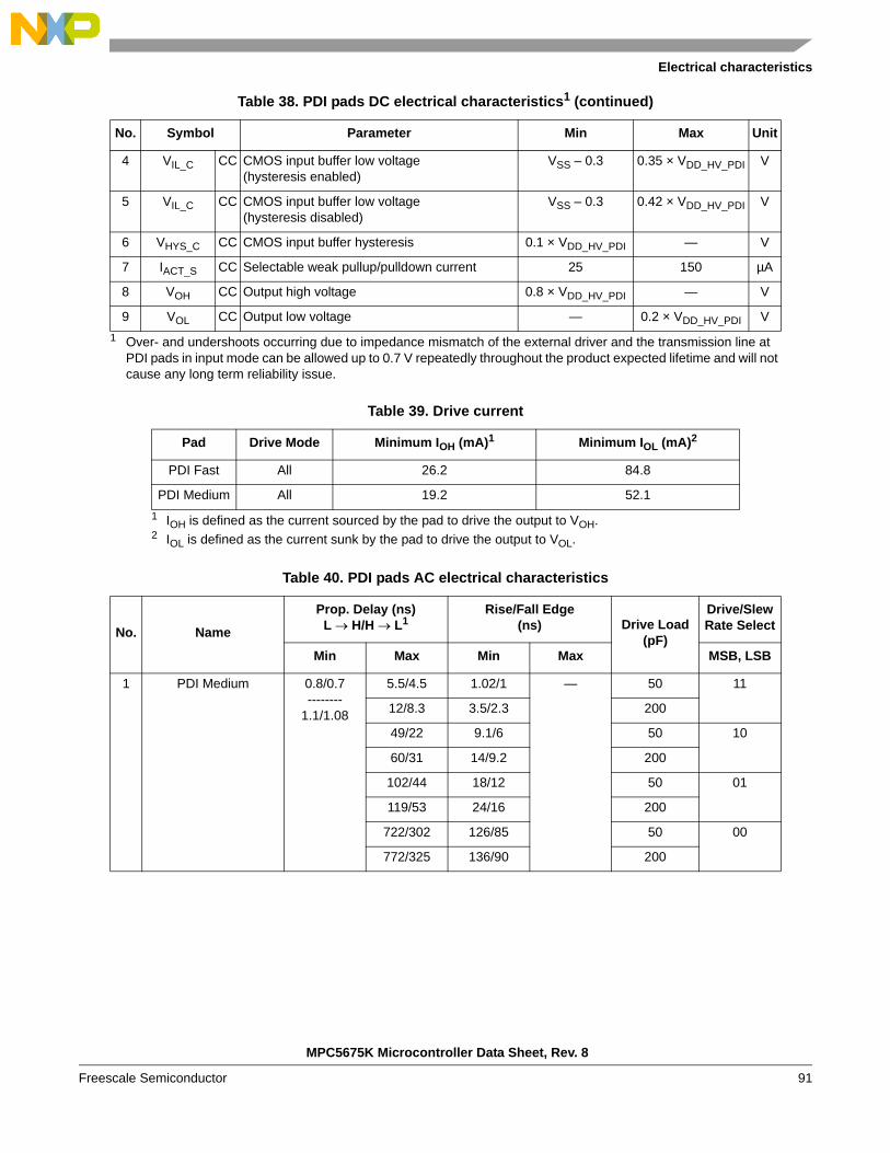
Electrical characteristics
MPC5675K Microcontroller Data Sheet, Rev. 8
Freescale Semiconductor 91
4 VIL_C CC CMOS input buffer low voltage(hysteresis enabled)
VSS – 0.3 0.35 × VDD_HV_PDI V
5 VIL_C CC CMOS input buffer low voltage(hysteresis disabled)
VSS – 0.3 0.42 × VDD_HV_PDI V
6 VHYS_C CC CMOS input buffer hysteresis 0.1 × VDD_HV_PDI — V
7 IACT_S CC Selectable weak pullup/pulldown current 25 150 µA
8 VOH CC Output high voltage 0.8 × VDD_HV_PDI — V
9 VOL CC Output low voltage — 0.2 × VDD_HV_PDI V
1 Over- and undershoots occurring due to impedance mismatch of the external driver and the transmission line at PDI pads in input mode can be allowed up to 0.7 V repeatedly throughout the product expected lifetime and will not cause any long term reliability issue.
Table 39. Drive current
Pad Drive Mode Minimum IOH (mA)1
1 IOH is defined as the current sourced by the pad to drive the output to VOH.
Minimum IOL (mA)2
2 IOL is defined as the current sunk by the pad to drive the output to VOL.
PDI Fast All 26.2 84.8
PDI Medium All 19.2 52.1
Table 40. PDI pads AC electrical characteristics
No. Name
Prop. Delay (ns) L H/H L1
Rise/Fall Edge (ns) Drive Load
(pF)
Drive/Slew Rate Select
Min Max Min Max MSB, LSB
1 PDI Medium 0.8/0.7--------
1.1/1.08
5.5/4.5 1.02/1 — 50 11
12/8.3 3.5/2.3 200
49/22 9.1/6 50 10
60/31 14/9.2 200
102/44 18/12 50 01
119/53 24/16 200
722/302 126/85 50 00
772/325 136/90 200
Table 38. PDI pads DC electrical characteristics1 (continued)
No. Symbol Parameter Min Max Unit

MPC5675K Microcontroller Data Sheet, Rev. 8
Electrical characteristics
Freescale Semiconductor92
3.18.1 PDI pad current specificationsThe power consumption of an I/O segment is dependent on the usage of the pins on a particular segment. The power consumption is the sum of all output pin currents for a particular segment. The output pin current can be calculated based on the voltage, frequency, and load on the pin.
3.18.2 Power Sequence Pin States for PDI Pads
2 PDI Fast 0.8/0.7--------
1.1/1.08
10/10 1.1/1.1 — 50 11
15/15 2.6/2.6 200
15/15 2.4/2.4 50 10
22/22 5/5 200
24/24 5/5 50 01
33/33 8/8 200
66/66 16/16 50 00
84/84 21/21 200
1 L H signifies low-to-high propagation delay and H L signifies high-to-low propagation delay.
Table 41. PDI pad current specifications
Pad Type Frequency
(MHz)Load (pF)
Voltage (V)
Drive/Slew Rate Select
Current(mA)
PDI Medium 66 50 3.6 11 8.7
33 50 3.6 10 3.8
20 50 3.6 01 2.3
3 50 3.6 00 0.38
3 200 3.6 00 1.5
PDI Fast 66 50 3.6 11 12
50 50 3.6 10 6.2
33 50 3.6 01 4.0
20 50 3.6 00 2.4
20 200 3.6 00 8.9
Table 42. Power sequence pin states for PDI pads
VDD_LV_COR VDD_HV_IO VDD_HV_PDI Pad Function
Low Low High Outputs drive high
Table 40. PDI pads AC electrical characteristics (continued)
No. Name
Prop. Delay (ns) L H/H L1
Rise/Fall Edge (ns) Drive Load
(pF)
Drive/Slew Rate Select
Min Max Min Max MSB, LSB

Electrical characteristics
MPC5675K Microcontroller Data Sheet, Rev. 8
Freescale Semiconductor 93
3.19 DRAM pad specificationsThis section specifies the electrical characteristics of the DRAM pads. Please refer to the tables in Section 2.2, Pin descriptions, for a cross reference between package pins and pad types.
DRAM pads feature list:
• Driver
— Configurable to support LPDDR half strength, LPDDR full strength, DDR1, DDR2 half strength, DDR2 full strength, and SDR modes.
— VDD_HV_DRAM range of
– 1.8 V nominal
– 2.5 V nominal
– 3.3 V nominal
• Receiver
— Differential or pseudo-differential input buffer in all DRAM pads
— All inputs are tolerant up to their VDD_HV_DRAM absolute maximum rating
— Data and strobe pads can be configured to support four signal termination options
– Infinite/no termination
– 50 – 75 – 150
The electrical data provided in Section 3.19, DRAM pad specifications, applies to the pads listed in Table 43.
All three pad types can be configured to support SDR, DDR, DDR2 half and full strength, and LPDDR half and full strength modes, according to Table 44.
Low High x Outputs Disabled
High Low Low Outputs Disabled
High Low High Outputs drive high
High High Low Normal Operation1
High High High Normal Operation
1 Normal operation except no drive current and input buffer output is unknown. The pad pre-drive circuitry will function normally but since VDD_HV_PDI is unpowered the outputs will not drive high even though the output PMOS can be enabled.
Table 43. DRAM pads
Name Voltage Used For Notes1
1 All pads can be configured to support LPDDR half strength, LPDDR full strength, DDR1, DDR2 half strength, DDR2 full strength, and SDR.
DRAM ACC 1.62 V–3.6 V I/O Bidirectional DDR pad
DRAM CLK 1.62 V–3.6 V O Output only differential clock driver pad
DRAM DQ 1.62 V–3.6 V I/O Bidirectional DDR pad with integrated ODT
Table 42. Power sequence pin states for PDI pads
VDD_LV_COR VDD_HV_IO VDD_HV_PDI Pad Function
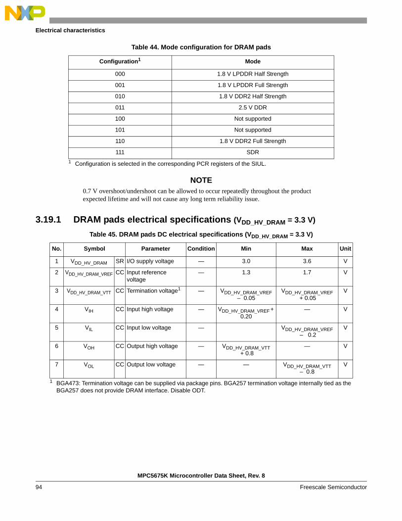
MPC5675K Microcontroller Data Sheet, Rev. 8
Electrical characteristics
Freescale Semiconductor94
NOTE0.7 V overshoot/undershoot can be allowed to occur repeatedly throughout the product expected lifetime and will not cause any long term reliability issue.
3.19.1 DRAM pads electrical specifications (VDD_HV_DRAM = 3.3 V)
Table 44. Mode configuration for DRAM pads
Configuration1
1 Configuration is selected in the corresponding PCR registers of the SIUL.
Mode
000 1.8 V LPDDR Half Strength
001 1.8 V LPDDR Full Strength
010 1.8 V DDR2 Half Strength
011 2.5 V DDR
100 Not supported
101 Not supported
110 1.8 V DDR2 Full Strength
111 SDR
Table 45. DRAM pads DC electrical specifications (VDD_HV_DRAM = 3.3 V)
No. Symbol Parameter Condition Min Max Unit
1 VDD_HV_DRAM SR I/O supply voltage — 3.0 3.6 V
2 VDD_HV_DRAM_VREF CC Input reference voltage
— 1.3 1.7 V
3 VDD_HV_DRAM_VTT CC Termination voltage1
1 BGA473: Termination voltage can be supplied via package pins. BGA257 termination voltage internally tied as the BGA257 does not provide DRAM interface. Disable ODT.
— VDD_HV_DRAM_VREF – 0.05
VDD_HV_DRAM_VREF + 0.05
V
4 VIH CC Input high voltage — VDD_HV_DRAM_VREF + 0.20
— V
5 VIL CC Input low voltage — VDD_HV_DRAM_VREF – 0.2
V
6 VOH CC Output high voltage — VDD_HV_DRAM_VTT + 0.8
— V
7 VOL CC Output low voltage — — VDD_HV_DRAM_VTT– 0.8
V
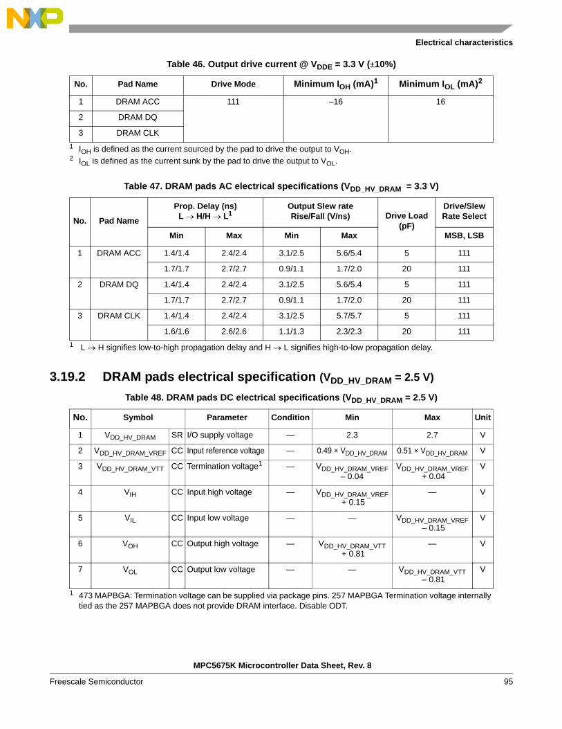
Electrical characteristics
MPC5675K Microcontroller Data Sheet, Rev. 8
Freescale Semiconductor 95
3.19.2 DRAM pads electrical specification (VDD_HV_DRAM = 2.5 V)
Table 46. Output drive current @ VDDE = 3.3 V (±10%)
No. Pad Name Drive Mode Minimum IOH (mA)1 Minimum IOL (mA)2
1 DRAM ACC 111 –16 16
2 DRAM DQ
3 DRAM CLK
1 IOH is defined as the current sourced by the pad to drive the output to VOH. 2 IOL is defined as the current sunk by the pad to drive the output to VOL.
Table 47. DRAM pads AC electrical specifications (VDD_HV_DRAM = 3.3 V)
No. Pad Name
Prop. Delay (ns) L H/H L1
1 L H signifies low-to-high propagation delay and H L signifies high-to-low propagation delay.
Output Slew rateRise/Fall (V/ns) Drive Load
(pF)
Drive/Slew Rate Select
Min Max Min Max MSB, LSB
1 DRAM ACC 1.4/1.4 2.4/2.4 3.1/2.5 5.6/5.4 5 111
1.7/1.7 2.7/2.7 0.9/1.1 1.7/2.0 20 111
2 DRAM DQ 1.4/1.4 2.4/2.4 3.1/2.5 5.6/5.4 5 111
1.7/1.7 2.7/2.7 0.9/1.1 1.7/2.0 20 111
3 DRAM CLK 1.4/1.4 2.4/2.4 3.1/2.5 5.7/5.7 5 111
1.6/1.6 2.6/2.6 1.1/1.3 2.3/2.3 20 111
Table 48. DRAM pads DC electrical specifications (VDD_HV_DRAM = 2.5 V)
No. Symbol Parameter Condition Min Max Unit
1 VDD_HV_DRAM SR I/O supply voltage — 2.3 2.7 V
2 VDD_HV_DRAM_VREF CC Input reference voltage — 0.49 × VDD_HV_DRAM 0.51 × VDD_HV_DRAM V
3 VDD_HV_DRAM_VTT CC Termination voltage1
1 473 MAPBGA: Termination voltage can be supplied via package pins. 257 MAPBGA Termination voltage internally tied as the 257 MAPBGA does not provide DRAM interface. Disable ODT.
— VDD_HV_DRAM_VREF – 0.04
VDD_HV_DRAM_VREF + 0.04
V
4 VIH CC Input high voltage — VDD_HV_DRAM_VREF + 0.15
— V
5 VIL CC Input low voltage — — VDD_HV_DRAM_VREF – 0.15
V
6 VOH CC Output high voltage — VDD_HV_DRAM_VTT + 0.81
— V
7 VOL CC Output low voltage — — VDD_HV_DRAM_VTT – 0.81
V
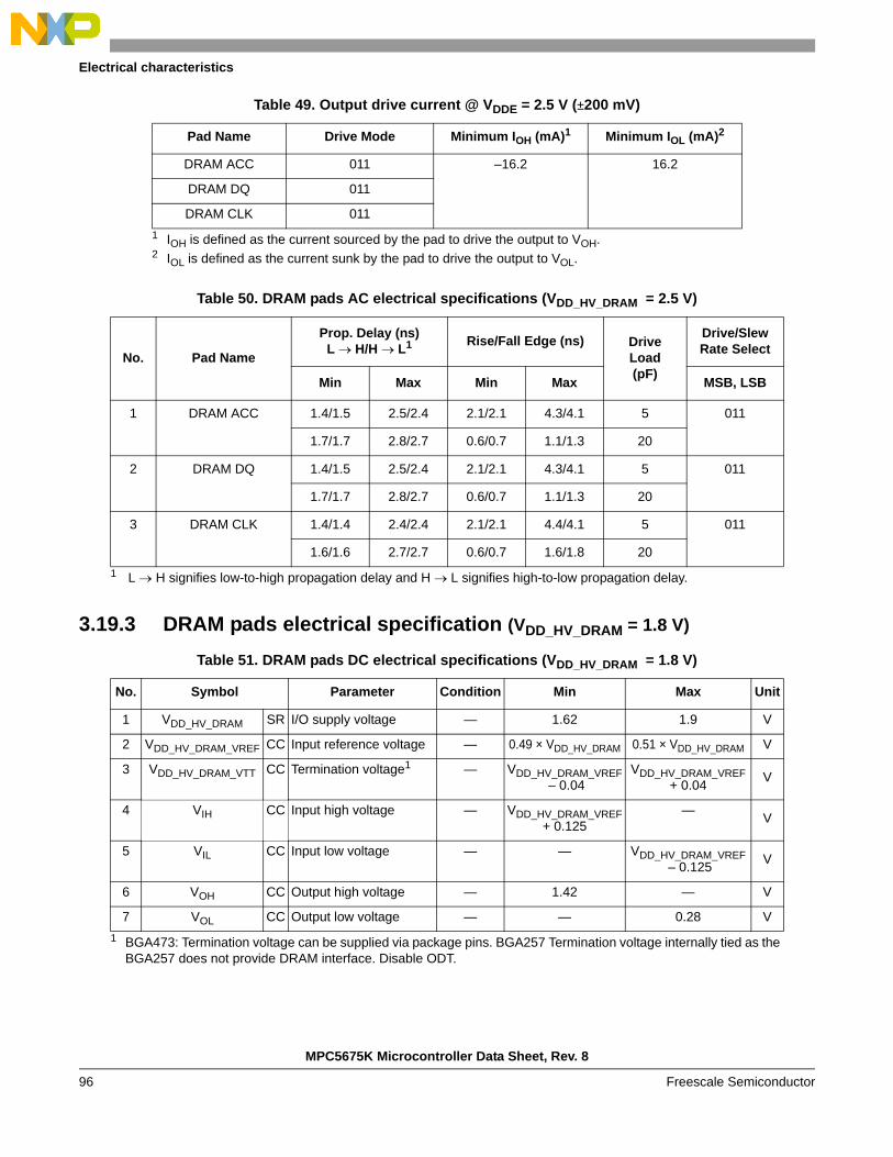
MPC5675K Microcontroller Data Sheet, Rev. 8
Electrical characteristics
Freescale Semiconductor96
3.19.3 DRAM pads electrical specification (VDD_HV_DRAM = 1.8 V)
Table 49. Output drive current @ VDDE = 2.5 V (±200 mV)
Pad Name Drive Mode Minimum IOH (mA)1
1 IOH is defined as the current sourced by the pad to drive the output to VOH.
Minimum IOL (mA)2
2 IOL is defined as the current sunk by the pad to drive the output to VOL.
DRAM ACC 011 –16.2 16.2
DRAM DQ 011
DRAM CLK 011
Table 50. DRAM pads AC electrical specifications (VDD_HV_DRAM = 2.5 V)
No. Pad Name
Prop. Delay (ns) L H/H L1
1 L H signifies low-to-high propagation delay and H L signifies high-to-low propagation delay.
Rise/Fall Edge (ns) Drive Load (pF)
Drive/Slew Rate Select
Min Max Min Max MSB, LSB
1 DRAM ACC 1.4/1.5 2.5/2.4 2.1/2.1 4.3/4.1 5 011
1.7/1.7 2.8/2.7 0.6/0.7 1.1/1.3 20
2 DRAM DQ 1.4/1.5 2.5/2.4 2.1/2.1 4.3/4.1 5 011
1.7/1.7 2.8/2.7 0.6/0.7 1.1/1.3 20
3 DRAM CLK 1.4/1.4 2.4/2.4 2.1/2.1 4.4/4.1 5 011
1.6/1.6 2.7/2.7 0.6/0.7 1.6/1.8 20
Table 51. DRAM pads DC electrical specifications (VDD_HV_DRAM = 1.8 V)
No. Symbol Parameter Condition Min Max Unit
1 VDD_HV_DRAM SR I/O supply voltage — 1.62 1.9 V
2 VDD_HV_DRAM_VREF CC Input reference voltage — 0.49 × VDD_HV_DRAM 0.51 × VDD_HV_DRAM V
3 VDD_HV_DRAM_VTT CC Termination voltage1
1 BGA473: Termination voltage can be supplied via package pins. BGA257 Termination voltage internally tied as the BGA257 does not provide DRAM interface. Disable ODT.
— VDD_HV_DRAM_VREF – 0.04
VDD_HV_DRAM_VREF + 0.04
V
4 VIH CC Input high voltage — VDD_HV_DRAM_VREF + 0.125
—V
5 VIL CC Input low voltage — — VDD_HV_DRAM_VREF – 0.125
V
6 VOH CC Output high voltage — 1.42 — V
7 VOL CC Output low voltage — — 0.28 V
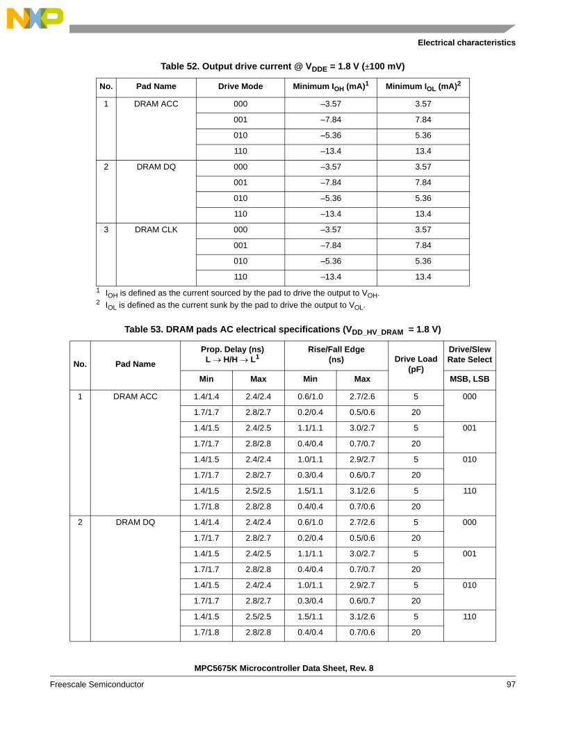
Electrical characteristics
MPC5675K Microcontroller Data Sheet, Rev. 8
Freescale Semiconductor 97
Table 52. Output drive current @ VDDE = 1.8 V (±100 mV)
No. Pad Name Drive Mode Minimum IOH (mA)1
1 IOH is defined as the current sourced by the pad to drive the output to VOH.
Minimum IOL (mA)2
2 IOL is defined as the current sunk by the pad to drive the output to VOL.
1 DRAM ACC 000 –3.57 3.57
001 –7.84 7.84
010 –5.36 5.36
110 –13.4 13.4
2 DRAM DQ 000 –3.57 3.57
001 –7.84 7.84
010 –5.36 5.36
110 –13.4 13.4
3 DRAM CLK 000 –3.57 3.57
001 –7.84 7.84
010 –5.36 5.36
110 –13.4 13.4
Table 53. DRAM pads AC electrical specifications (VDD_HV_DRAM = 1.8 V)
No. Pad Name
Prop. Delay (ns) L H/H L1
Rise/Fall Edge (ns) Drive Load
(pF)
Drive/Slew Rate Select
Min Max Min Max MSB, LSB
1 DRAM ACC 1.4/1.4 2.4/2.4 0.6/1.0 2.7/2.6 5 000
1.7/1.7 2.8/2.7 0.2/0.4 0.5/0.6 20
1.4/1.5 2.4/2.5 1.1/1.1 3.0/2.7 5 001
1.7/1.7 2.8/2.8 0.4/0.4 0.7/0.7 20
1.4/1.5 2.4/2.4 1.0/1.1 2.9/2.7 5 010
1.7/1.7 2.8/2.7 0.3/0.4 0.6/0.7 20
1.4/1.5 2.5/2.5 1.5/1.1 3.1/2.6 5 110
1.7/1.8 2.8/2.8 0.4/0.4 0.7/0.6 20
2 DRAM DQ 1.4/1.4 2.4/2.4 0.6/1.0 2.7/2.6 5 000
1.7/1.7 2.8/2.7 0.2/0.4 0.5/0.6 20
1.4/1.5 2.4/2.5 1.1/1.1 3.0/2.7 5 001
1.7/1.7 2.8/2.8 0.4/0.4 0.7/0.7 20
1.4/1.5 2.4/2.4 1.0/1.1 2.9/2.7 5 010
1.7/1.7 2.8/2.7 0.3/0.4 0.6/0.7 20
1.4/1.5 2.5/2.5 1.5/1.1 3.1/2.6 5 110
1.7/1.8 2.8/2.8 0.4/0.4 0.7/0.6 20

MPC5675K Microcontroller Data Sheet, Rev. 8
Electrical characteristics
Freescale Semiconductor98
3.19.4 DRAM Pad Current SpecificationsThe power consumption of an I/O segment is dependent on the usage of the pins on a particular segment. The power consumption is the sum of all output pin currents for a particular segment. The output pin current can be calculated based on the voltage, frequency, and load on the pin.
3 DRAM CLK 1.4/1.4 2.4/2.4 0.4/0.6 2.7/2.7 5 000
1.6/1.6 2.7/2.7 0.7/0.9 1.8/3.4 20
1.4/1.4 2.4/2.4 1.1/1.1 3.0/2.8 5 001
1.7/1.7 2.7/2.7 0.3/0.4 1.0/1.1 20
1.4/1.4 2.4/2.4 0.9/1.1 3.0/2.8 5 010
1.6/1.6 2.7/2.7 0.3/0.4 0.9/1.0 20
1.4/1.4 2.5/2.5 1.5/1.2 3.2/2.6 5 110
1.7/1.7 2.7/2.7 0.4/0.4 1.1/1.2 20
1 L H signifies low-to-high propagation delay and H L signifies high-to-low propagation delay.
Table 53. DRAM pads AC electrical specifications (VDD_HV_DRAM (continued) = 1.8 V)
No. Pad Name
Prop. Delay (ns) L H/H L1
Rise/Fall Edge (ns) Drive Load
(pF)
Drive/Slew Rate Select
Min Max Min Max MSB, LSB

Electrical characteristics
MPC5675K Microcontroller Data Sheet, Rev. 8
Freescale Semiconductor 99
3.19.5 Power Sequence Pin States for DRAM Pads
Table 54. DRAM pad current specifications
Pad Type Frequency
(MHz)Load (pF)
Voltage (V)
Drive/Slew Rate Select
Current(mA)
DRAM DQ /DRAM ACC
45 5 1.8 LPDDR_HS (010)1
1 LPDDR_HS = LPDDR half strength, LPDDR_FS = LPDDR full strength, DDR2_HS = DDR2 half strength, DDR2_FS = DDR2 half strength.
0.74
45 5 1.8 LPDDR_FS (110)1 0.9
45 5 1.8 DDR2_HS (010)1 0.81
45 5 1.8 DDR2_FS (110)1 1.26
45 10 1.8 LPDDR_HS (010)1 1.14
45 10 1.8 LPDDR_FS (110)1 1.28
45 10 1.8 DDR2_HS (010)1 1.21
45 10 1.8 DDR2_FS (110)1 1.59
45 20 1.8 LPDDR_HS (010)1 1.97
45 20 1.8 LPDDR_FS (110)1 2.08
45 20 1.8 DDR2_HS (010)1 2.02
45 20 1.8 DDR2_FS (110)1 2.33
90 5 1.8 LPDDR_HS (010)1 1.41
90 5 1.8 LPDDR_FS (110)1 1.73
90 5 1.8 DDR2_HS (010)1 1.56
90 5 1.8 DDR2_FS (110)1 2.42
90 10 1.8 LPDDR_HS (010)1 2.19
90 10 1.8 LPDDR_FS (110)1 2.45
90 10 1.8 DDR2_HS (010)1 2.32
90 10 1.8 DDR2_FS (110)1 3.05
90 20 1.8 LPDDR_HS (010)1 3.77
90 20 1.8 LPDDR_FS (110)1 3.98
90 20 1.8 DDR2_HS (010)1 3.87
90 20 1.8 DDR2_FS (110)1 4.46
Table 55. Power sequence pin states for DRAM pads
VDD_LV_COR VDD_HV_IO VDD_HV_PDI Pad Function
Low Low High Outputs Disabled
Low High x Outputs Disabled
High Low Low Outputs Disabled
High Low High Outputs Disabled

MPC5675K Microcontroller Data Sheet, Rev. 8
Electrical characteristics
Freescale Semiconductor100
3.20 RESET characteristics
3.20.1 RESET pin characteristics
3.20.2 RESET_SUP_B pin characteristics
3.21 Reset sequenceThis section shows the duration for different reset sequences. It describes the different reset sequences and it specifies the start conditions and the end indication for the reset sequences depending on internal or external VREG mode.
3.21.1 Reset sequence durationTable 58 specifies the minimum and the maximum reset sequence duration for the five different reset sequences described in Section 3.21.2, Reset sequence description.
High High Low Normal Operation1
High High High Normal Operation
1 Normal operation except no drive current and input buffer output is unknown. The pad pre-drive circuitry will function normally but since VDD_HV_DRAM is unpowered, the outputs will not drive high even though the output PMOS can be enabled. DDR pad is only guaranteed to operate and be in compliance with Jedec standards, when all three power supplies, VDD_LV_COR, VDD_HV_IO and VDD_HV_DRAM are fully powered up.
Table 56. RESET pin characteristics
No. Symbol Parameter Conditions Min Max Unit
1 WFRST SR RESET pulse is sure to be filtered — — 70 ns
2 WNFRST SR RESET pulse is sure not to be filtered — 400 — ns
Table 57. RESET_SUP_B pin characteristics
No. Symbol Parameter Conditions Min Max Unit
1 WFRST SR RESET_SUP_B pulse is sure to be filtered (there is no internal filter on this pin)
— — 0 ns
2 TRSTSUP SR RESET_SUP_B release by an external delay/monitor circuit after all supplies are stable
— 0 — ns
Table 55. Power sequence pin states for DRAM pads
VDD_LV_COR VDD_HV_IO VDD_HV_PDI Pad Function

Electrical characteristics
MPC5675K Microcontroller Data Sheet, Rev. 8
Freescale Semiconductor 101
3.21.2 Reset sequence descriptionThe figures in this section show the internal states of the MPC5675K during the five different reset sequences. The doted lines in the figures indicate the starting point and the end point for which the duration is specified in Table 58. The start point and end point conditions as well as the reset trigger mapping to the different reset sequences is specified in Section 3.21.3, Reset sequence trigger mapping.
With the beginning of DRUN mode, the first instruction is fetched and executed. At this point, application execution starts and the internal reset sequence is finished.
The following figures show the internal states of the MPC5675K during the execution of the reset sequence and the possible states of the RESET signal pin.
NOTERESET is a bidirectional pin. The voltage level on this pin can either be driven low by an external reset generator or by the MPC5675K internal reset circuitry. A high level on this pin can only be generated by an external pullup resistor which is strong enough to overdrive the weak internal pulldown resistor. The rising edge on RESET in the following figures indicates the time when the device stops driving it low. The reset sequence durations given in Table 58 are applicable only if the internal reset sequence is not prolonged by an external reset generator keeping RESET asserted low beyond the last PHASE3.
Figure 12. Destructive reset sequence, BIST enabled
Table 58. RESET sequences
No. Symbol ParameterTReset
UnitMin Typ Max1
1 The maximum value is applicable only if the reset sequence duration is not prolonged by an extended assertion of RESET by an external reset generator.
1 TDRB CC Destructive Reset Sequence, BIST enabled 50 60 70 ms
2 TDR CC Destructive Reset Sequence, BIST disabled 40 400 1000 µs
3 TERLB CC External Reset Sequence Long, BIST enabled 50 60 70 ms
4 TFRL CC Functional Reset Sequence Long 40 300 600 µs
5 TFRS CC Functional Reset Sequence Short 1 3 10 µs
PHASE0 PHASE1,2 PHASE3 PHASE1,2 PHASE3 DRUNBIST
Reset Sequence Trigger
Reset Sequence Start Condition
RESET
Establish Flash Device SelfMBIST LBIST
ApplicationIRC and
PWRInit Test
SetupConfig
FlashInit
DeviceConfig Execution
TDRB, min < TRESET < TDRB, max
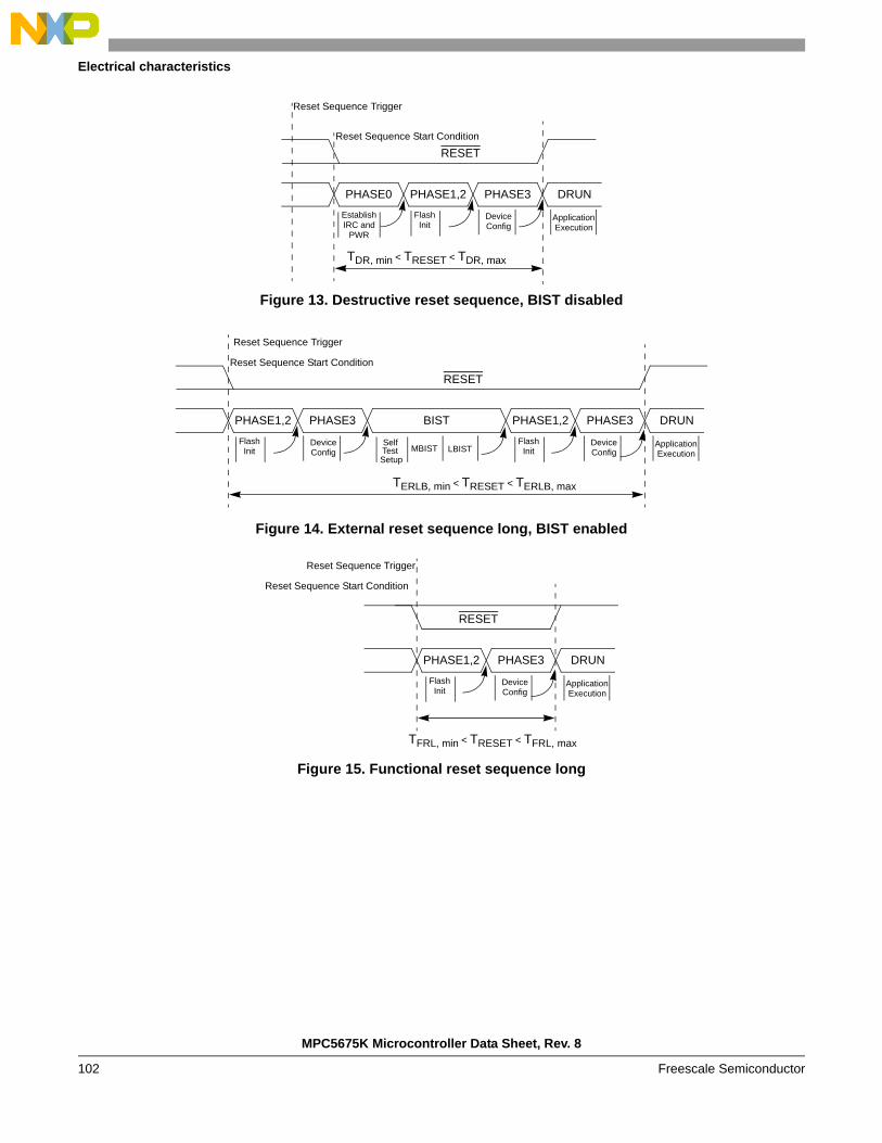
MPC5675K Microcontroller Data Sheet, Rev. 8
Electrical characteristics
Freescale Semiconductor102
Figure 13. Destructive reset sequence, BIST disabled
Figure 14. External reset sequence long, BIST enabled
Figure 15. Functional reset sequence long
PHASE0 PHASE1,2 PHASE3 DRUN
Reset Sequence Trigger
Reset Sequence Start Condition
RESET
Establish Flash Device ApplicationIRC and
PWRInit Config Execution
TDR, min < TRESET < TDR, max
PHASE1,2 PHASE3 PHASE1,2 PHASE3 DRUNBIST
Reset Sequence Trigger
Reset Sequence Start Condition
RESET
Flash Device SelfMBIST LBIST
ApplicationInit Test
SetupConfig
FlashInit
DeviceConfig Execution
TERLB, min < TRESET < TERLB, max
PHASE1,2 PHASE3 DRUN
Reset Sequence Trigger
Reset Sequence Start Condition
RESET
ApplicationFlashInit
DeviceConfig Execution
TFRL, min < TRESET < TFRL, max

Electrical characteristics
MPC5675K Microcontroller Data Sheet, Rev. 8
Freescale Semiconductor 103
Figure 16. Functional reset sequence short
The reset sequences shown in Figure 15 and Figure 16 are triggered by functional reset events. RESET is driven low during these two reset sequences only if the corresponding functional reset source (which triggered the reset sequence) was enabled to drive RESET low for the duration of the internal reset sequence. See the RGM_FBRE register in the MPC5675K Reference Manual for more information.
3.21.3 Reset sequence trigger mappingThe following table shows the possible trigger events for the different reset sequences, depending on the VREG mode (external or internal). It specifies the reset sequence start conditions as well as the reset sequence end indications that are the basis for the timing data provided in Table 58.
PHASE3 DRUN
Reset Sequence Trigger
Reset Sequence Start Condition
RESET
Application Execution
TFRS, min < TRESET < TFRS, max

MPC5675K Microcontroller Data Sheet, Rev. 8
Electrical characteristics
Freescale Semiconductor104
Table 59. Reset sequence trigger—reset sequence
ResetSequence
Trigger
VR
EG
Mo
de1
1 VREG Mode: I = Internal VREG Mode, E = External VREG Mode.
Reset Sequence
Start Condition
Reset Sequence
End Indication
Reset Sequence
Destructive Reset Sequence, BIST enabled2
2 Whether BIST is executed or not depends on device configuration data stored in the shadow sector of the NVM.
Destructive Reset Sequence, BIST disabled2
External Reset Sequence Long, BIST enabled
Functional Reset Sequence Long
Functional Reset Sequence Short
All active internal destructive reset sources(LVDs or internal HVD during power-up and during operation)
I Section 3.21.4.1, Internal VREG mode
Release of RESET3
3 End of the internal reset sequence (as specified in Table 58) can only be observed by release of RESET if it is not held low externally beyond the end of the internal sequence which would prolong the internal reset PHASE3 until RESET is released externally.
triggers cannot trigger
cannot trigger
cannot trigger
E Section 3.21.4.2,
External VREG mode
cannot trigger
cannot trigger
cannot trigger
Assertion of RESET_SUP4
4 In external VREG mode only.
Assertion of RESET5
5 The assertion of RESET can only trigger a reset sequence if the device was running (RESET released) before. RESET does not gate a Destructive Reset Sequence, BIST enabled or a Destructive Reset Sequence, BIST disabled. However, it can prolong these sequences if RESET is held low externally beyond the end of the internal sequence (beyond PHASE3).
I/E Section 3.21.4.3,
External reset via RESET
cannot trigger triggers6
6 If RESET is configured for long reset (default) and if BIST is enabled via device configuration data stored in the shadow sector of the NVM.
triggers7
7 If RESET is configured for long reset (default) and if BIST is disabled via device configuration data stored in the shadow sector of the NVM.
triggers8
All internal functional reset sources configured for long reset
I/E Sequence starts with
internal reset
trigger
Release of RESET9
cannot trigger cannot trigger
triggers cannot trigger
All internal functional reset sources configured for short reset
I/E cannot trigger cannot trigger
cannot trigger
triggers

Electrical characteristics
MPC5675K Microcontroller Data Sheet, Rev. 8
Freescale Semiconductor 105
3.21.4 Reset sequence—start conditionThe impact of the voltage thresholds on the starting point of the internal reset sequence are becoming important if the voltage rails / signals ramp up with a very slow slew rate compared to the overall reset sequence duration.
3.21.4.1 Internal VREG mode
Figure 17 shows the voltage threshold that determines the start of the Destructive Reset Sequence, BIST enabled and the start for the Destructive Reset Sequence, BIST disabled. The last voltage rail crossing the levels shown in Figure 17 determines the start of the reset times specified in Table 58.
Figure 17. Reset sequence start in internal VREG mode
3.21.4.2 External VREG mode
Figure 18 and Figure 19 show the voltage thresholds that determine the start of the Destructive Reset Sequence, BIST enabled and the start for the Destructive Reset Sequence, BIST disabled.
NOTERESET_SUP must not be released unless VDD_LV_xxx is within its valid range of operation. RESET_SUP input circuitry needs a valid VDD_HV_IO rail in order to detect a high level on RESET_SUP.
8 If RESET is configured for short reset. 9 Internal reset sequence can only be observed by state of RESET if bidirectional RESET functionality is enabled for the functional
reset source which triggered the reset sequence.
Table 60. Voltage thresholds
Variable name Value
Vmin LvdReg – 3.5%
Vmax LvdReg + 3.5%
Supply Rail VDD_HV_PMUVDD_HV_IO
VDD_HV_FLASHVDD_HV_ADV
Vmax
Supply rail
Vmin
V
t
TReset, min starts here
TReset, max starts here

MPC5675K Microcontroller Data Sheet, Rev. 8
Electrical characteristics
Freescale Semiconductor106
Figure 18. External VREG mode, RESET_SUP rises after VDD_HV_xxx are stable
Figure 19. External VREG mode, RESET_SUP rises with VDD_HV_xxx
NOTEIn case RESET_SUP has reached a valid high level before VDD_HV_IO is stable, the reset sequence will start as documented in Figure 19 as the RESET_SUP input circuitry needs a valid VDD_HV_IO rail in order to detect a high level on RESET_SUP.
VDD_HV_PMUV
t
0.8 × VDD_HV_IO
RESET_SUPV
t
TReset, min starts here
TReset, max starts here
VDD_HV_IOVDD_HV_FLASHVDD_HV_ADV
0.2 × VDD_HV_IO
Min VDD_HV_XXX
Min VDD_LV_XXX
TRSTSUP
VDD_LV_COREVDD_LV_PLL
VDD_HV_PMUV
t
LvdReg + 3.5%
RESET_SUPV
t
TReset, min starts here
TReset, max starts here
VDD_HV_IOVDD_HV_FLASHVDD_HV_ADV
LvdReg – 3.5%

Electrical characteristics
MPC5675K Microcontroller Data Sheet, Rev. 8
Freescale Semiconductor 107
3.21.4.3 External reset via RESET
Figure 20 shows the voltage thresholds that determine the start of the reset sequences initiated by the assertion of RESET as specified in Table 59.
Figure 20. Reset sequence start via RESET assertion
3.21.5 External watchdog windowIf the application design requires the use of an external watchdog the data provided in Section 3.21, Reset sequence can be used to determine the correct positioning of the trigger window for the external watchdog. Figure 21 shows the relationships between the minimum and the maximum duration of a given reset sequence and the position of an external watchdog trigger window.
Figure 21. Reset sequence—external watchdog trigger window position
3.22 Peripheral timing characteristics
3.22.1 SDRAM (DDR)The MPC5675K memory controller supports three types of DDR devices:
• DDR-1 (SSTL_2 class II interface)
• DDR-2 (SSTL_18 interface)
• LPDDR/Mobile-DDR (1.8V I/O supply voltage)
0.65 × VDD_HV_IO
RESET_SUP
V
t
TReset, min starts here
TReset, max starts here
0.352 × VDD_HV_IO
Internal reset sequenceStart condition (signal or voltage rail)
Earliestapplicationstart
Latestapplicationstart
Application time requiredto prepare watchdog trigger
TWDStart, min
TWDStart, max
TReset, min
TReset, max
Watchdog needs to be triggered within this window
External Watchdog window open
External Watchdog window open
External watchdog window closed
Basic application init
Basic application init
Application running
Application running
Watchdog trigger
External watchdog window closed

MPC5675K Microcontroller Data Sheet, Rev. 8
Electrical characteristics
Freescale Semiconductor108
JEDEC standards define the minimum set of requirements for compliant memory devices:
• JEDEC STANDARD, DDR2 SDRAM SPECIFICATION, JESD79-2C, MAY 2006
• JEDEC STANDARD, Double Data Rate (DDR) SDRAM Specification, JESD79E, May 2005
• JEDEC STANDARD, Low Power Double Data Rate (LPDDR) SDRAM Specification, JESD79-4, May 2006
The MPC5675K supports the configuration of two output drive strengths for DDR2 and LPDDR:
• Full drive strength
• Half drive strength (intended for lighter loads or point-to-point environments)
The MPC5675K memory controller supports dynamic on-die termination in the host device and in the DDR2 memory device.
This section includes AC specifications for all DDR SDRAM pins. The DC parameters are specified in the Section 3.19, DRAM pad specifications.
3.22.1.1 DDR and DDR2 SDRAM AC timing specifications
Figure 22 shows the DDR SDRAM write timing.
Table 61. DDR and DDR2 (DDR2-400) SDRAM timing specifications
At recommended operating conditions with VDD_MEM_IO of 5%
No. Symbol Parameter Min Max Unit
1 tCK CC Clock cycle time, CL = x — 90 MHz
2 VIX-AC CC MCK AC differential crosspoint voltage1
1 Measured with clock pin loaded with differential 100 termination resistor.
VDD_MEM_IO× 0.5 – 0.1
VDD_MEM_IO× 0.5 + 0.1
V
3 tCH CC CK HIGH pulse width1, 2
2 All transitions measured at mid-supply (VDD_MEM_IO/2).
0.47 0.53 tCK
4 tCL CC CK LOW pulse width1, 2 0.47 0.53 tCK
5 tDQSS CC Skew between MCK and DQS transitions2, 3
3 Measured with all outputs except the clock loaded with 50 termination resistor to VDD_MEM_IO/2.
0.25 0.25 tCK
6 tOS(base) CC Address and control output setup time relative to MCK rising edge2, 3
(tCK/2 – 750) ps
7 tOH(base) CC Address and control output hold time relative to MCK rising edge2, 3
(tCK/2 – 750) — ps
8 tDS1(base) CC DQ and DM output setup time relative to DQS2, 3 (tCK/4 – 500) — ps
9 tDH1(base) CC DQ and DM output hold time relative to DQS2, 3 (tCK/4 – 500) — ps
10 tDQSQ CC DQS-DQ skew for DQS and associated DQ inputs2 –(tCK/4 – 600) (tCK/4 – 600) ps

Electrical characteristics
MPC5675K Microcontroller Data Sheet, Rev. 8
Freescale Semiconductor 109
Figure 22. DDR write timing
Figure 23 and Figure 24 show the DDR SDRAM read timing.
Figure 23. DDR read timing, DQ vs. DQS
Figure 24. DDR read timing, DQSEN
Figure 25 provides the AC test load for the DDR bus.
MCK
tCH tCL
DQS
tDQSS
DQ, DM (out)
tDS tDH
tCK
DQS (in)
Any DQ (in)
tDQSQ tDQSQ
MCK
DQS (in)
tOS tOH
Command
Address
Read
tDQSEN (min)
tDQSEN
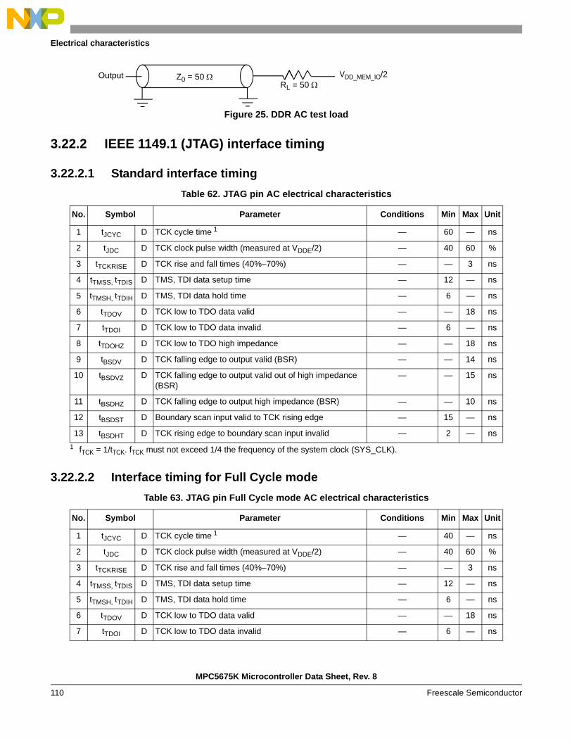
MPC5675K Microcontroller Data Sheet, Rev. 8
Electrical characteristics
Freescale Semiconductor110
Figure 25. DDR AC test load
3.22.2 IEEE 1149.1 (JTAG) interface timing
3.22.2.1 Standard interface timing
3.22.2.2 Interface timing for Full Cycle mode
Table 62. JTAG pin AC electrical characteristics
No. Symbol Parameter Conditions Min Max Unit
1 tJCYC D TCK cycle time 1
1 fTCK = 1/tTCK. fTCK must not exceed 1/4 the frequency of the system clock (SYS_CLK).
— 60 — ns
2 tJDC D TCK clock pulse width (measured at VDDE/2) — 40 60 %
3 tTCKRISE D TCK rise and fall times (40%–70%) — — 3 ns
4 tTMSS, tTDIS D TMS, TDI data setup time — 12 — ns
5 tTMSH, tTDIH D TMS, TDI data hold time — 6 — ns
6 tTDOV D TCK low to TDO data valid — — 18 ns
7 tTDOI D TCK low to TDO data invalid — 6 — ns
8 tTDOHZ D TCK low to TDO high impedance — — 18 ns
9 tBSDV D TCK falling edge to output valid (BSR) — — 14 ns
10 tBSDVZ D TCK falling edge to output valid out of high impedance (BSR)
— — 15 ns
11 tBSDHZ D TCK falling edge to output high impedance (BSR) — — 10 ns
12 tBSDST D Boundary scan input valid to TCK rising edge — 15 — ns
13 tBSDHT D TCK rising edge to boundary scan input invalid — 2 — ns
Table 63. JTAG pin Full Cycle mode AC electrical characteristics
No. Symbol Parameter Conditions Min Max Unit
1 tJCYC D TCK cycle time 1 — 40 — ns
2 tJDC D TCK clock pulse width (measured at VDDE/2) — 40 60 %
3 tTCKRISE D TCK rise and fall times (40%–70%) — — 3 ns
4 tTMSS, tTDIS D TMS, TDI data setup time — 12 — ns
5 tTMSH, tTDIH D TMS, TDI data hold time — 6 — ns
6 tTDOV D TCK low to TDO data valid — — 18 ns
7 tTDOI D TCK low to TDO data invalid — 6 — ns
Output Z0 = 50 RL = 50
VDD_MEM_IO/2

Electrical characteristics
MPC5675K Microcontroller Data Sheet, Rev. 8
Freescale Semiconductor 111
Figure 26. JTAG test clock input timing
Figure 27. JTAG test access port timing
1 fTCK = 1/tTCK. fTCK needs to be smaller than the system clock (SYS_CLK). This frequency is valid only in special modes where TDO is sampled at the next falling edge for Core0/1 Nexus TAPs and hence full cycle is given to TDO for settling before it is sampled.
TCK
1
2
2
3
3
TCK
4
5
6
7 8
TMS, TDI
TDO
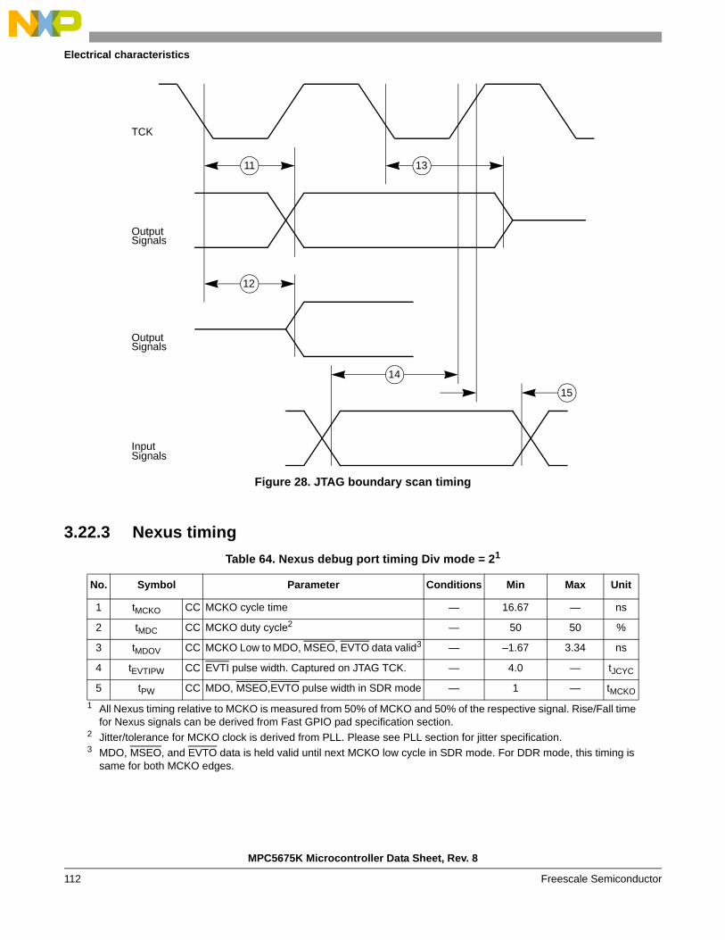
MPC5675K Microcontroller Data Sheet, Rev. 8
Electrical characteristics
Freescale Semiconductor112
Figure 28. JTAG boundary scan timing
3.22.3 Nexus timing
Table 64. Nexus debug port timing Div mode = 21
1 All Nexus timing relative to MCKO is measured from 50% of MCKO and 50% of the respective signal. Rise/Fall time for Nexus signals can be derived from Fast GPIO pad specification section.
No. Symbol Parameter Conditions Min Max Unit
1 tMCKO CC MCKO cycle time — 16.67 — ns
2 tMDC CC MCKO duty cycle2
2 Jitter/tolerance for MCKO clock is derived from PLL. Please see PLL section for jitter specification.
— 50 50 %
3 tMDOV CC MCKO Low to MDO, MSEO, EVTO data valid3
3 MDO, MSEO, and EVTO data is held valid until next MCKO low cycle in SDR mode. For DDR mode, this timing is same for both MCKO edges.
— –1.67 3.34 ns
4 tEVTIPW CC EVTI pulse width. Captured on JTAG TCK. — 4.0 — tJCYC
5 tPW CC MDO, MSEO,EVTO pulse width in SDR mode — 1 — tMCKO
TCK
OutputSignals
InputSignals
OutputSignals
11
12
13
14
15

Electrical characteristics
MPC5675K Microcontroller Data Sheet, Rev. 8
Freescale Semiconductor 113
Figure 29. Nexus SDR (Even divisor) timing
Figure 30. Nexus SDR output timing for DIV=3
Table 65. Nexus debug port timing Divide by 3 SDR mode1
1 MDO, MSEO, and EVTO data is held valid until next MCKO low cycle in SDR mode. Rise/Fall time for Nexus signals can be derived from Fast GPIO pad specification section.
No. Symbol Parameter Conditions Min Max Unit
1 tMCKO CC MCKO cycle time — 16.67 — ns
2 tMDC CC MCKO duty cycle2
2 Jitter/tolerance for MCKO clock is derived from PLL. Please see PLL section for jitter specification.
— 33 66 %
3 tMDOV CC MCKO Low to MDO, MSEO, EVTO data valid — –1.67 3.34 ns
4 tEVTIPW CC EVTI pulse width. Captured on JTAG TCK. — 4.0 — tJCYC
5 tPW CC MDO, MSEO,EVTO pulse width in SDR mode — 1 — tMCKO
1
2
MCKO
MDOMSEO
EVTOOutput Data Valid
3
EVTI4
5
1
2
MCKO
MDOMSEO
EVTOOutput Data Valid
3
EVTI4
5
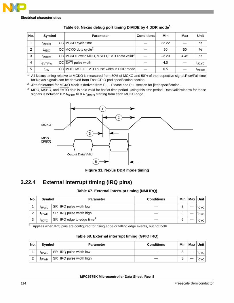
MPC5675K Microcontroller Data Sheet, Rev. 8
Electrical characteristics
Freescale Semiconductor114
Figure 31. Nexus DDR mode timing
3.22.4 External interrupt timing (IRQ pins)
Table 66. Nexus debug port timing DIVIDE by 4 DDR mode1
1 All Nexus timing relative to MCKO is measured from 50% of MCKO and 50% of the respective signal.Rise/Fall time for Nexus signals can be derived from Fast GPIO pad specification section.
No. Symbol Parameter Conditions Min Max Unit
1 tMCKO CC MCKO cycle time — 22.22 — ns
2 tMDC CC MCKO duty cycle2
2 Jitter/tolerance for MCKO clock is derived from PLL. Please see PLL section for jitter specification.
— 50 50 %
3 tMDOV CC MCKO Low to MDO, MSEO, EVTO data valid3
3 MDO, MSEO, and EVTO data is held valid for half of time period. Using this time period, Data valid window for these signals is between 0.2 tMCKO to 0.4 tMCKO starting from each MCKO edge.
— –2.23 4.45 ns
4 tEVTIPW CC EVTI pulse width — 4.0 — tJCYC
5 tPW CC MDO, MSEO,EVTO pulse width in DDR mode — 0.5 — tMCKO
Table 67. External interrupt timing (NMI IRQ)
No. Symbol Parameter Conditions Min Max Unit
1 tIPWL SR IRQ pulse width low — 3 — tCYC
2 tIPWH SR IRQ pulse width high — 3 — tCYC
3 tICYC SR IRQ edge to edge time1
1 Applies when IRQ pins are configured for rising edge or falling edge events, but not both.
— 6 — tCYC
Table 68. External interrupt timing (GPIO IRQ)
No. Symbol Parameter Conditions Min Max Unit
1 tIPWL SR IRQ pulse width low — 3 — tCYC
2 tIPWH SR IRQ pulse width high — 3 — tCYC
1
2
MCKO
MDOMSEO
Output Data Valid
3
5
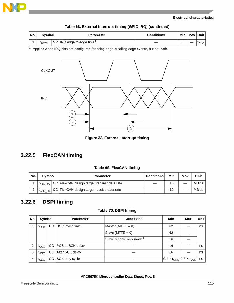
Electrical characteristics
MPC5675K Microcontroller Data Sheet, Rev. 8
Freescale Semiconductor 115
Figure 32. External interrupt timing
3.22.5 FlexCAN timing
3.22.6 DSPI timing
3 tICYC SR IRQ edge to edge time1 — 6 — tCYC
1 Applies when IRQ pins are configured for rising edge or falling edge events, but not both.
Table 69. FlexCAN timing
No. Symbol Parameter Conditions Min Max Unit
1 fCAN_TX CC FlexCAN design target transmit data rate — 10 — MBit/s
2 fCAN_RX CC FlexCAN design target receive data rate — 10 — MBit/s
Table 70. DSPI timing
No. Symbol Parameter Conditions Min Max Unit
1 tSCK CC DSPI cycle time Master (MTFE = 0) 62 — ns
Slave (MTFE = 0) 62 —
Slave receive only mode1 16 —
2 tCSC CC PCS to SCK delay — 16 — ns
3 tASC CC After SCK delay — 16 — ns
4 tSDC CC SCK duty cycle — 0.4 × tSCK 0.6 × tSCK ns
Table 68. External interrupt timing (GPIO IRQ) (continued)
No. Symbol Parameter Conditions Min Max Unit
CLKOUT
IRQ
1
2
3

MPC5675K Microcontroller Data Sheet, Rev. 8
Electrical characteristics
Freescale Semiconductor116
5 tA CC Slave access time SS active to SOUT valid — 40 ns
6 tDIS CC Slave SOUT disable time SS inactive to SOUT High-Z or invalid — 10 ns
7 tPCSC CC PCSx to PCSS time — 13 — ns
8 tPASC CC PCSS to PCSx time — 13 — ns
9 tSUI CC Data setup time for inputs Master (MTFE = 0) 20 — ns
Slave 2 —
Master (MTFE = 1, CPHA = 0) 5 —
Master (MTFE = 1, CPHA = 1) 20 —
10 tHI CC Data hold time for inputs Master (MTFE = 0) –5 — ns
Slave 4 —
Master (MTFE = 1, CPHA = 0) 11 —
Master (MTFE = 1, CPHA = 1) –5 —
11 tSUO CC Data valid (after SCK edge) Master (MTFE = 0) — 4 ns
Slave — 23
Master (MTFE = 1, CPHA = 0) — 11
Master (MTFE = 1, CPHA = 1) — 5
12 tHO CC Data hold time for outputs Master (MTFE = 0) –2 — ns
Slave 6 —
Master (MTFE = 1, CPHA = 0) 6 —
Master (MTFE = 1, CPHA = 1) –2 —
13 tDT CC Delay after Transfer (minimum CS negation time)
Continuous mode Non-continuos mode2
62134
——
ns
1 Slave Receive Only Mode can operate at a maximum frequency of 60 MHz. Note that in this mode, the DSPI can receive data on SIN, but no valid data is transmitted on SOUT.
2 In non-continuous mode, this value is always tSCK × DSPI_CTARn[DT] × DSPI_CTARn[PDT]. The minimum permissible value of DT is 2 and the minimum permissible value of PDT is 1. See the DSPI chapter of the MPC5675K Reference Manual for more information.
Table 70. DSPI timing (continued)
No. Symbol Parameter Conditions Min Max Unit

Electrical characteristics
MPC5675K Microcontroller Data Sheet, Rev. 8
Freescale Semiconductor 117
Figure 33. DSPI classic SPI timing—master, CPHA = 0
Figure 34. DSPI classic SPI timing—master, CPHA = 1
Data Last DataFirst Data
First Data Data Last Data
SIN
SOUT
PCSx
SCK Output
4
9
12
1
11
10
4
SCK Output
(CPOL=0)
(CPOL=1)
32
Data Last DataFirst DataSIN
SOUT
12 11
10
Last DataDataFirst Data
SCK Output
SCK Output
PCSx
9
(CPOL=0)
(CPOL=1)
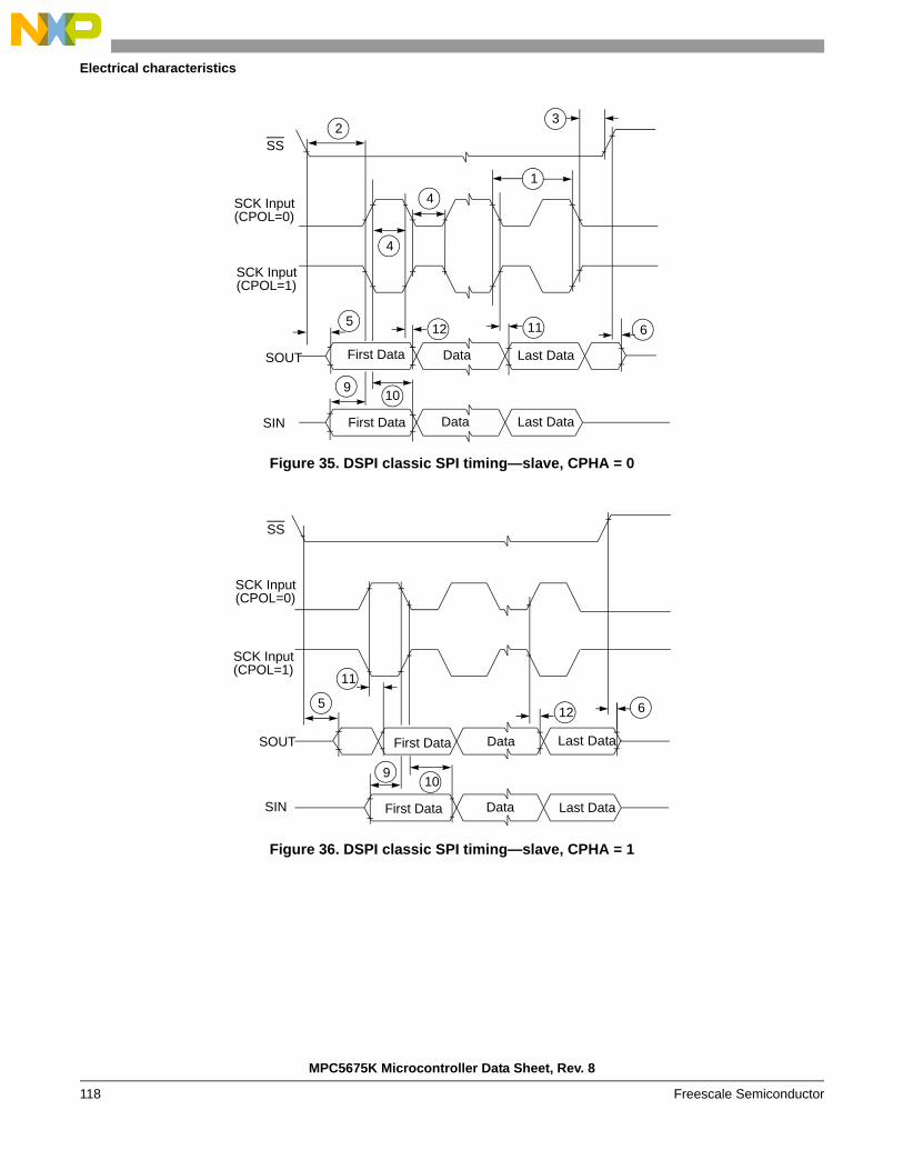
MPC5675K Microcontroller Data Sheet, Rev. 8
Electrical characteristics
Freescale Semiconductor118
Figure 35. DSPI classic SPI timing—slave, CPHA = 0
Figure 36. DSPI classic SPI timing—slave, CPHA = 1
Last DataFirst Data
3
4
1
Data
Data
SIN
SOUT
SS
4
5 6
9
11
10
12
SCK Input
First Data Last Data
SCK Input
2
(CPOL=0)
(CPOL=1)
5 6
9
12
11
10
Last Data
Last DataSIN
SOUT
SS
First Data
First Data
Data
Data
SCK Input
SCK Input
(CPOL=0)
(CPOL=1)
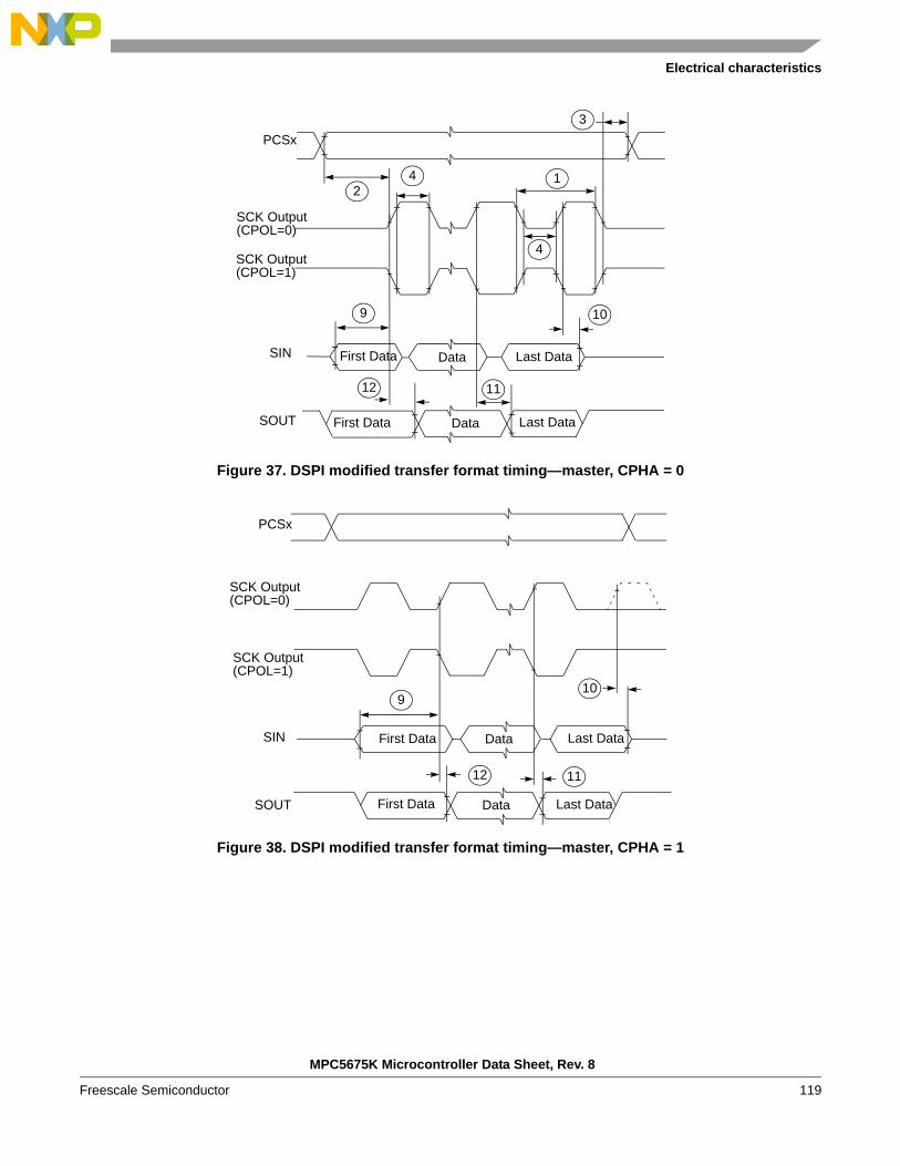
Electrical characteristics
MPC5675K Microcontroller Data Sheet, Rev. 8
Freescale Semiconductor 119
Figure 37. DSPI modified transfer format timing—master, CPHA = 0
Figure 38. DSPI modified transfer format timing—master, CPHA = 1
PCSx
3
14
10
4
9
12 11
SCK Output
SCK Output
SIN
SOUT
First Data Data Last Data
First Data Data Last Data
2
(CPOL=0)
(CPOL=1)
PCSx
109
12 11
SCK Output
SCK Output
SIN
SOUT
First Data Data Last Data
First Data Data Last Data
(CPOL=0)
(CPOL=1)
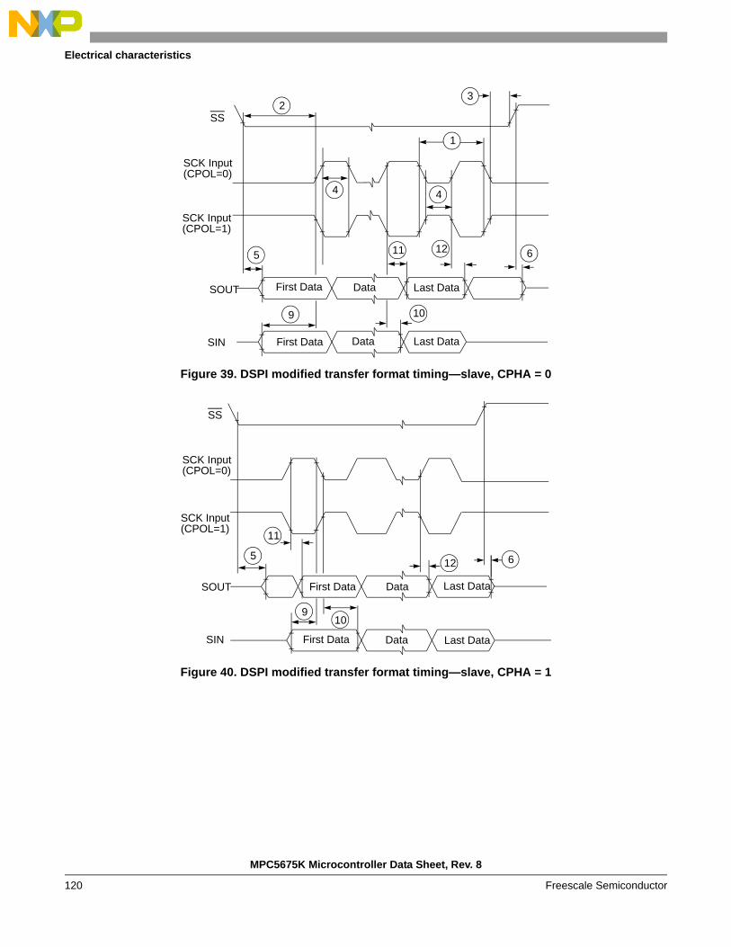
MPC5675K Microcontroller Data Sheet, Rev. 8
Electrical characteristics
Freescale Semiconductor120
Figure 39. DSPI modified transfer format timing—slave, CPHA = 0
Figure 40. DSPI modified transfer format timing—slave, CPHA = 1
Last DataFirst Data
3
4
1
Data
Data
SIN
SOUT
SS
4
5 6
9
11
10
SCK Input
First Data Last Data
SCK Input
2
(CPOL=0)
(CPOL=1)
12
5 6
9
12
11
10
Last Data
Last DataSIN
SOUT
SS
First Data
First Data
Data
Data
SCK Input
SCK Input
(CPOL=0)
(CPOL=1)

Electrical characteristics
MPC5675K Microcontroller Data Sheet, Rev. 8
Freescale Semiconductor 121
Figure 41. Example of non-continuous format (CPHA = 1, CONT = 0)
Figure 42. Example of continuous transfer (CPHA = 1, CONT = 1)
Figure 43. DSPI PCS strobe (PCSS) timing
3.22.7 PDI timing
Table 71. PDI electrical characteristics
No. Symbol Parameter Conditions Min Max Unit
1 tPDI_CLOCK SR PDI clock period — 15 — ns
SCK
PCSx
SCK
Master SOUT
Master SIN
(CPOL = 0)
(CPOL = 1)
2 23
13
SCK
PCS
SCK
Master SOUT
Master SIN
(CPOL = 0)
(CPOL = 1)
(CPOL = 0)SCK
3 22
PCSx
7 8
PCSS
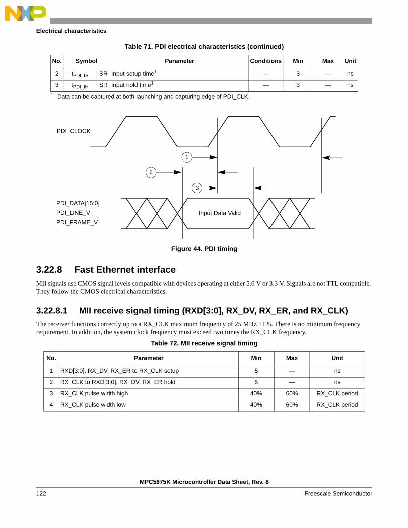
MPC5675K Microcontroller Data Sheet, Rev. 8
Electrical characteristics
Freescale Semiconductor122
Figure 44. PDI timing
3.22.8 Fast Ethernet interfaceMII signals use CMOS signal levels compatible with devices operating at either 5.0 V or 3.3 V. Signals are not TTL compatible. They follow the CMOS electrical characteristics.
3.22.8.1 MII receive signal timing (RXD[3:0], RX_DV, RX_ER, and RX_CLK)
The receiver functions correctly up to a RX_CLK maximum frequency of 25 MHz +1%. There is no minimum frequency requirement. In addition, the system clock frequency must exceed two times the RX_CLK frequency.
2 tPDI_IS SR Input setup time1 — 3 — ns
3 tPDI_IH SR Input hold time1 — 3 — ns
1 Data can be captured at both launching and capturing edge of PDI_CLK.
Table 72. MII receive signal timing
No. Parameter Min Max Unit
1 RXD[3:0], RX_DV, RX_ER to RX_CLK setup 5 — ns
2 RX_CLK to RXD[3:0], RX_DV, RX_ER hold 5 — ns
3 RX_CLK pulse width high 40% 60% RX_CLK period
4 RX_CLK pulse width low 40% 60% RX_CLK period
Table 71. PDI electrical characteristics (continued)
No. Symbol Parameter Conditions Min Max Unit
PDI_CLOCK
2
3
PDI_DATA[15:0]
Input Data ValidPDI_LINE_V
PDI_FRAME_V
1
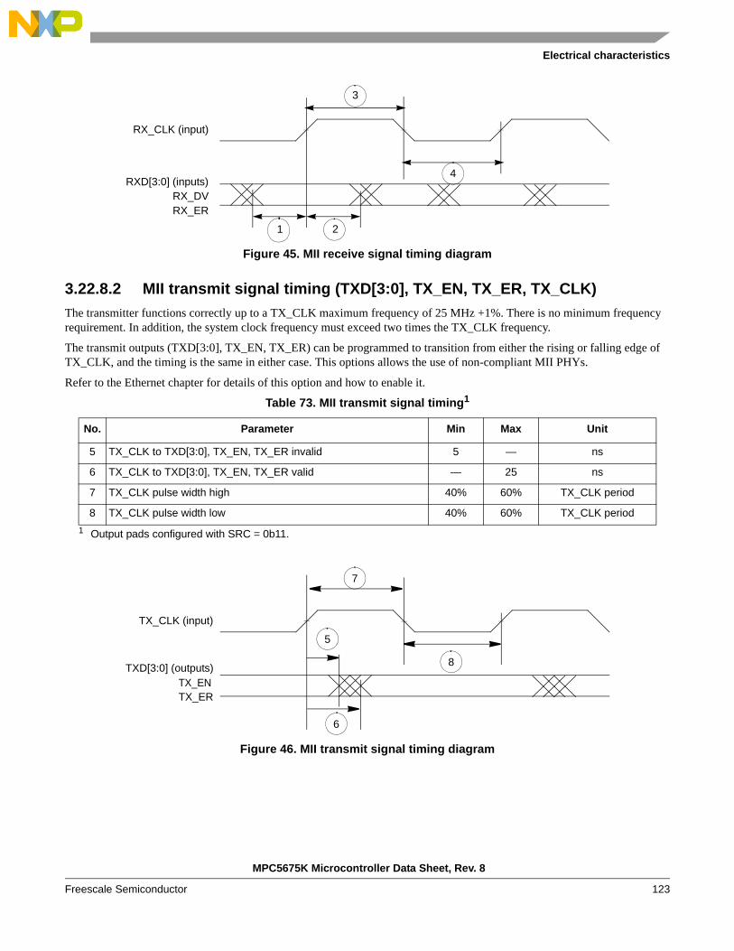
Electrical characteristics
MPC5675K Microcontroller Data Sheet, Rev. 8
Freescale Semiconductor 123
Figure 45. MII receive signal timing diagram
3.22.8.2 MII transmit signal timing (TXD[3:0], TX_EN, TX_ER, TX_CLK)
The transmitter functions correctly up to a TX_CLK maximum frequency of 25 MHz +1%. There is no minimum frequency requirement. In addition, the system clock frequency must exceed two times the TX_CLK frequency.
The transmit outputs (TXD[3:0], TX_EN, TX_ER) can be programmed to transition from either the rising or falling edge of TX_CLK, and the timing is the same in either case. This options allows the use of non-compliant MII PHYs.
Refer to the Ethernet chapter for details of this option and how to enable it.
Figure 46. MII transmit signal timing diagram
Table 73. MII transmit signal timing1
1 Output pads configured with SRC = 0b11.
No. Parameter Min Max Unit
5 TX_CLK to TXD[3:0], TX_EN, TX_ER invalid 5 — ns
6 TX_CLK to TXD[3:0], TX_EN, TX_ER valid — 25 ns
7 TX_CLK pulse width high 40% 60% TX_CLK period
8 TX_CLK pulse width low 40% 60% TX_CLK period
1 2
RX_CLK (input)
RXD[3:0] (inputs)RX_DVRX_ER
3
4
6
TX_CLK (input)
TXD[3:0] (outputs)TX_ENTX_ER
5
7
8

MPC5675K Microcontroller Data Sheet, Rev. 8
Electrical characteristics
Freescale Semiconductor124
3.22.8.3 MII async inputs signal timing (CRS and COL)
Figure 47. MII async inputs timing diagram
3.22.8.4 MII serial management channel timing (MDIO and MDC)
The FEC functions correctly with a maximum MDC frequency of 5 MHz.
Table 74. MII async inputs signal timing1
1 Output pads configured with SRC = 0b11.
No. Parameter Min Max Unit
9 CRS, COL minimum pulse width 1.5 — TX_CLK period
Table 75. MII serial management channel timing1
1 Output pads configured with SRC = 0b11.
No. Parameter Min Max Unit
10 MDC falling edge to MDIO output invalid (minimum propagation delay) 0 — ns
11 MDC falling edge to MDIO output valid (max prop delay) — 25 ns
12 MDIO (input) to MDC rising edge setup 10 — ns
13 MDIO (input) to MDC rising edge hold 0 — ns
14 MDC pulse width high 40% 60% MDC period
15 MDC pulse width low 40% 60% MDC period
CRS, COL
9

Electrical characteristics
MPC5675K Microcontroller Data Sheet, Rev. 8
Freescale Semiconductor 125
Figure 48. MII serial management channel timing diagram
3.22.9 External Bus Interface (EBI) timing
Table 76. EBI timing
No. Symbol Parameter45 MHz (Ext. Bus Freq)1
Unit NotesMin Max
1 tC CC D_CLKOUT period 22.2 — ns Signals are measured at 50% VDDE.
2 tCDC CC D_CLKOUT duty cycle 45% 55% tC —
3 tCRT CC D_CLKOUT rise time — — ns —
4 tCFT CC D_CLKOUT fall time — — ns —
5 tCOH CC D_CLKOUT posedge to output signal invalid or high Z (hold time)
D_ADD[9:30]D_BDIPD_CS[0:3]D_DAT[0:15]D_OED_RD_WRD_TAD_TSD_WE[0:3]/D_BE[0:3]
1.0 — ns —
11
MDC (output)
MDIO (output)
1213
MDIO (input)
10
14 15

MPC5675K Microcontroller Data Sheet, Rev. 8
Electrical characteristics
Freescale Semiconductor126
6 tCOV CC D_CLKOUT posedge to output signal valid (output delay)
D_ADD[9:30]D_BDIPD_CS[0:3]D_DAT[0:15]D_OED_RD_WRD_TAD_TSD_WE[0:3]/D_BE[0:3]
— 10 ns —
7 tCIS CC Input signal valid to D_CLKOUT posedge (setup time)
D_ADD[9:30]D_DAT[0:15]D_RD_WRD_TAD_TS
7.5 — ns —
8 tCIH CC D_CLKOUT posedge to input signal invalid (hold time)
D_ADD[9:30]D_DAT[0:15]D_RD_WRD_TAD_TS
1.0 — ns —
9 tAPW CC D_ALE pulse width 6.5 — ns The timing is for asynchronous external memory system.
10 tAAI CC D_ALE negated to address invalid 1.5 — ns • The timing is for asynchronous external memory system.
• ALE is measured at 50% of VDDE.
1 Speed is the nominal maximum frequency. Maximum core speed allowed is 180 MHz plus frequency modulation (FM).
Table 76. EBI timing (continued)
No. Symbol Parameter45 MHz (Ext. Bus Freq)1
Unit NotesMin Max

Electrical characteristics
MPC5675K Microcontroller Data Sheet, Rev. 8
Freescale Semiconductor 127
Figure 49. D_CLKOUT timing
Figure 50. Synchronous output timing
1
2
2
3
4
D_CLKOUT
VDDE / 2
VOL_F
VOH_F
65
5
D_CLKOUT
Bus
5
Output Signal
Output
VDDE / 2
VDDE / 2
VDDE / 2
6
5
Output Signal VDDE / 2
6

MPC5675K Microcontroller Data Sheet, Rev. 8
Electrical characteristics
Freescale Semiconductor128
Figure 51. Synchronous input timing
Figure 52. ALE signal timing
7
8
D_CLKOUT
InputBus
7
8
InputSignal
VDDE / 2
VDDE / 2
VDDE / 2
ipg_clk
D_CLKOUT
D_ALE
D_TS
ADDR DATAD_ADD/D_DAT
9
10

Electrical characteristics
MPC5675K Microcontroller Data Sheet, Rev. 8
Freescale Semiconductor 129
3.22.10 I2C timing
Table 77. I2C SCL and SDA input timing specifications
No. Symbol ParameterValue
UnitMin Max
1 — D Start condition hold time 2 — IP bus cycle1
1 Inter Peripheral Clock is the clock at which the I2C peripheral is working in the device.
2 — D Clock low time 8 — IP bus cycle1
3 — D Data hold time 0.0 — ns
4 — D Clock high time 4 — IP bus cycle1
5 — D Data setup time 0.0 — ns
6 — D Start condition setup time (for repeated start condition only) 2 — IP bus cycle1
7 — D Stop condition setup time 2 — IP bus cycle1
Table 78. I2C SCL and SDA output timing specifications
No. Symbol ParameterValue
UnitMin Max
11
1 Programming IBFD (I2C bus Frequency Divider) with the maximum frequency results in the minimum output timings listed. The I2C interface is designed to scale the data transition time, moving it to the middle of the SCL low period. The actual position is affected by the prescale and division values programmed in IFDR.
— D Start condition hold time 6 — IP bus cycle2
2 Inter Peripheral Clock is the clock at which the I2C peripheral is working in the device.
21 — D Clock low time 10 — IP bus cycle1
33
3 Because SCL and SDA are open-drain-type outputs, which the processor can only actively drive low, the time SCL or SDA takes to reach a high level depends on external signal capacitance and pullup resistor values.
— D SCL/SDA rise time — 99.6 ns
41 — D Data hold time 7 — IP bus cycle1
51 — D SCL/SDA fall time — 99.5 ns
61 — D Clock high time 10 — IP bus cycle1
71 — D Data setup time 2 — IP bus cycle1
81 — D Start condition setup time (for repeated start condition only) 20 — IP bus cycle1
91 — D Stop condition setup time 10 — IP bus cycle1

MPC5675K Microcontroller Data Sheet, Rev. 8
Electrical characteristics
Freescale Semiconductor130
Figure 53. I2C input/output timing
3.22.11 LINFlex timingThe maximum bit rate is 1.875 MBit/s.
SCL
SDA
1
2
3
4
56
7 8 9
Package characteristics
MPC5675K Microcontroller Data Sheet, Rev. 8
Freescale Semiconductor 131
4 Package characteristics
4.1 Package mechanical data
4.1.1 257 MAPBGA

MPC5675K Microcontroller Data Sheet, Rev. 8
Package characteristics
Freescale Semiconductor132
Figure 54. 257 MAPBGA mechanical data (1 of 2)

Package characteristics
MPC5675K Microcontroller Data Sheet, Rev. 8
Freescale Semiconductor 133
Figure 55. 257 MAPBGA mechanical data (2 of 2)

MPC5675K Microcontroller Data Sheet, Rev. 8
Package characteristics
Freescale Semiconductor134
4.1.2 473 MAPBGA
Figure 56. 473 MAPBGA package mechanical data (1 of 3)

Package characteristics
MPC5675K Microcontroller Data Sheet, Rev. 8
Freescale Semiconductor 135
Figure 57. 473 MAPBGA package mechanical data (2 of 3)

MPC5675K Microcontroller Data Sheet, Rev. 8
Package characteristics
Freescale Semiconductor136
Figure 58. 473 MAPBGA package mechanical data (3 of 3)

Orderable parts
MPC5675K Microcontroller Data Sheet, Rev. 8
Freescale Semiconductor 137
5 Orderable parts
6 Reference documents1. Nexus (IEEE-ISTO 5001™—2008)
2. Measurement of emission of ICs—IEC 61967-2
3. Measurement of emission of ICs—IEC 61967-4
4. Measurement of immunity of ICs—IEC 62132-4
5. Semiconductor Equipment and Materials International3081 Zanker RoadSan Jose, CA 95134 USA(408) 943-6900
6. JEDEC specifications are available at http://www.jedec.org
7. MIL-SPEC and EIA/JESD (JEDEC) specifications are available from Global Engineering Documents at 800-854-7179 or 303-397-7956.
8. C.E. Triplett and B. Joiner, “An Experimental Characterization of a 272 PBGA Within an Automotive Engine Controller Module,” Proceedings of SemiTherm, San Diego, 1998, pp. 47–54.
9. G. Kromann, S. Shidore, and S. Addison, “Thermal Modeling of a PBGA for Air-Cooled Applications,” Electronic Packaging and Production, pp. 53–58, March 1998.
10. B. Joiner and V. Adams, “Measurement and Simulation of Junction to Board Thermal Resistance and Its Application in Thermal Modeling,” Proceedings of SemiTherm, San Diego, 1999, pp. 212–220.
7 Document revision historyTable 79 summarizes revisions to this document.
Beginning with Rev. 4, this revision history uses clickable cross-references for ease of navigation. The numbers and titles in each cross-reference are relative to the latest published release.
M PC F
Note: Not all options are available on all devices.
5675K
Qualification status
Core code
Device number
Device feature setDevice revision
Temperature range
V = –40 °C to 105 °C
Device revision
F0 = Fab and Mask
Operating frequency
1 = 150 MHzTape and reel status
R = Tape and reel(blank) = Trays
Qualification status
P = Pre-qualificationM = Fully spec. qualified, general market flowS = Fully spec. qualified, automotive flow
F0 M
Temperature range
MM
Package identifier
2 R
Operating frequency
Tape and reel status
Device feature set
F = FlexRayPackage identifier
MM = 257 BGA
2 = 180 MHz
M = –40 °C to 125 °C MS= 473 BGA(ambient)

MPC5675K Microcontroller Data Sheet, Rev. 8
Document revision history
Freescale Semiconductor138
Table 79. Revision history
Revision Date Description of Changes
1 6 Oct 2009 Initial release.
2 6 Dec 2009 Updated ball map tables, pin mux tables, supply and system pin tables. Added PMC specifications.
3 2 Jul 2010 Updated ball map tables, pin mux tables, supply and system pin tables. Updated pad specifications. Added reset specifications section.
4 30 Apr 2011 Removed thickness dimension from package diagrams on cover page.Added footnote “Do not connect pin directly to a power supply or ground” for MDO[0:15]
and MSEO[0:1] pins to Table 9 (257 MAPBGA pin multiplexing) and Table 10 (473 MAPBGA pin multiplexing).
In Table 17 (PMC electrical specifications):
• Added minimum and maximum slew rate specifications for LvdReg. • Removed LvdC minimum and maximum hysteresis specifications • Removed HvdC minimum and maximum hysteresis specifications • Corrected HvcD nominal hysteresis from 1.32 to 1.36 In Table 18 (VRC SMPS recommended external devices), updated specifications for
device Q (FET). Renamed Section 3.9, Supply current characteristics (was “Power dissipation and current
consumption”).Renamed Table 19 (Current consumption characteristics) (was “Power dissipation
characteristics”).In Table 19 (Current consumption characteristics): • Updated ADC current consumption to 1.2 mA per ADC plus 0.7 mA (2.0 mA total) for
ADC0. • Updated Run IDD to 900 mA max. Updated Accuracy specification in Table 20 (Temperature sensor electrical
characteristics): changed “TJ = –40 °C to TA = 25 °C” to “TJ = –40 °C to TA = 125 °C,” removed row “TJ = TA to 125 °C”.
In Table 21 (Main oscillator electrical characteristics), added symbol name FXOSCHS for Oscillator frequency specification.
Removed “Typical” figures for these specifications.Added footnote “ADC0 includes 0.7 mA dissipation for the temperature sensor (TSENS).”
In Table 22 (FMPLL electrical characteristics), added minimum and maximum values for specification fFREE, “Free running frequency.”
In Table 23 (RC oscillator electrical characteristics): • Added specification IRCTRIM “Internal RC oscillator trimming step.” • Removed specification RCTRIM “Post trim accuracy: The variation of the PTF from the
16 MHz” (specification replaced by IRCTRIM “Internal RC oscillator trimming step”). In Table 24 (ADC conversion characteristics), updated Gain Error (GNE) to “min = –4 max
= +4 LSB“. Added Table 30 (Code flash write access timing) and Table 31 (Data flash write access
timing).
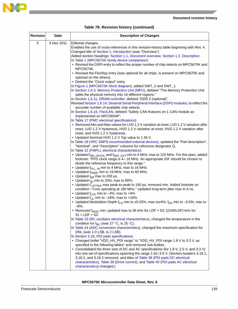
Document revision history
MPC5675K Microcontroller Data Sheet, Rev. 8
Freescale Semiconductor 139
5 6 Dec 2011 Editorial changes.Enabled the use of cross-references in this revision-history table beginning with Rev. 4.Changed title of Section 1, Introduction (was “Overview”).Added section headings: Section 1.1, Document overview, Section 1.2, DescriptionIn Table 1 (MPC5675K family device comparison): • Revised the DSPI entry to reflect the proper number of chip selects on MPC5675K and
MPC5674K. • Revised the FlexRay entry (was optional for all chips, is present on MPC5675K and
optional on the others). • Deleted the “Clock output” entry.In Figure 1 (MPC5675K block diagram), added SWT_0 and SWT_1.In Section 1.6.3, Memory Protection Unit (MPU), deleted "The Memory Protection Unit
splits the physical memory into 16 different regions."In Section 1.6.11, DRAM controller, deleted “DDR 2 (optional)”.Revised Section 1.6.14, Deserial Serial Peripheral Interface (DSPI) modules, to reflect the
accurate number of available chip selects.In Section 1.6.16, FlexCAN, deleted “Safety CAN features on 1 CAN module as
implemented on MPC5604P”.In Table 17 (PMC electrical specifications): • Removed Min and Max values for LVD 1.2 V variation at reset, LVD 1.2 V variation after
reset, LVD 1.2 V hysteresis, HVD 1.2 V variation at reset, HVD 1.2 V variation after reset, and HVD 1.2 V hysteresis.
• Updated Nominal HVD 1.2 V Typ value to 1.36 V.In Table 18 (VRC SMPS recommended external devices), updated the "Part description",
“Nominal”, and "Description" columns for reference designator Q.In Table 22 (FMPLL electrical characteristics): • Updated fREF_CRYSTAL and fREF_EXT min to 4 MHz; max to 120 MHz. For this spec, added
footnote: “PFD clock range is 4– 16 MHz. An appropriate IDF should be chosen to divide the reference frequency to this range.”
• Updated fPLL_IN min to 4 MHz; max to 16 MHz. • Updated fFREE min to 19 MHz; max to 60 MHz. • Updated tlpll max to 200 µs. • Updated tdc min to 20%; max to 80%. • Updated CJITTER max peak-to-peak to 160 ps; removed min. Added footnote on
condition: “Core operating at 180 MHz.” Updated long-term jitter max to 6 ns. • Updated fLCK min to –4%; max to +4%. • Updated fUL min to –16%; max to +16%. • Updated Modulation Depth fCS min to ±0.25%; max to±4%; fDS min to –0.5%; max to
–8%. • Removed fMOD min; updated max to 35 kHz for LDF > 63; (2240/LDF) kHz for
31 < LDF < 63. In Table 23 (RC oscillator electrical characteristics), changed the temperature in the
condition for fRC (was 27 C, is 25 C).In Table 24 (ADC conversion characteristics), changed the maximum specification for
DNL (was 1.0 LSB, is 2 LSB).In Section 3.18, PDI pads specifications: • Changed bullet “VDD_HV_PDI range” to “VDD_HV_PDI range 1.8 V to 3.3 V, as
specified in the following tables” and removed sub-bullets. • Consolidated the three sets of DC and AC specifications (for 1.8 V, 2.5 V, and 3.3 V)
into one set of specifications spanning the range 1.62–3.6 V. (Section headers 3.18.1, 3.18.2, and 3.18.3 removed, and titles of Table 38 (PDI pads DC electrical characteristics), Table 39 (Drive current), and Table 40 (PDI pads AC electrical characteristics) changed.)
Table 79. Revision history (continued)
Revision Date Description of Changes

MPC5675K Microcontroller Data Sheet, Rev. 8
Document revision history
Freescale Semiconductor140
5(cont.)
6 Dec 2011 In Section 3.19, DRAM pad specifications, added the note “0.7 V overshoot/undershoot can be allowed to occur repeatedly throughout the product expected lifetime and will not cause any long term reliability issue.”
In Table 45 (DRAM pads DC electrical specifications (VDD_HV_DRAM = 3.3 V)): • Updated VDD_HV_DRAM_VTT minimum value to VDD_HV_DRAM_VREF – 0.05 (changed
“×” to “–”) • Updated VIL maximum value to VDD_HV_DRAM_VREF – 0.2 (changed “×” to “–”) • Removed ODT conditions for VOH and VOL. • Updated VOL maximum value to VDD_HV_DRAM_VTT – 0.8 (changed “×” to “–”)In Table 48 (DRAM pads DC electrical specifications (VDD_HV_DRAM = 2.5 V)), removed
ODT conditions for VOH and VOL.In Table 51 (DRAM pads DC electrical specifications (VDD_HV_DRAM = 1.8 V)): • Changed the minimum specification for VDD_HV_DRAM (was 1.7 V, is 1.62 V). • Removed ODT conditions for VOH and VOL. • Updated VOH minimum value to 1.42 V • Updated VOL maximum value to 0.28 VAdded Section 3.20.2, RESET_SUP_B pin characteristics. Updated Note under Section 3.21.4.2, External VREG mode. Updated Figure 18 (External VREG mode, RESET_SUP rises after VDD_HV_xxx are
stable) to add TRSTSUP.Added Section 3.22.2.1, Standard interface timing, and revised the specifications in
Table 62 (JTAG pin AC electrical characteristics).Added Section 3.22.2.2, Interface timing for Full Cycle mode.Replaced the contents of Section 3.22.3, Nexus timing, with the following: • Table 64 (Nexus debug port timing Div mode = 2) and Figure 29 (Nexus SDR (Even
divisor) timing) • Table 65 (Nexus debug port timing Divide by 3 SDR mode) and Figure 30 (Nexus SDR
output timing for DIV=3) • Table 66 (Nexus debug port timing DIVIDE by 4 DDR mode) and Figure 31 (Nexus
DDR mode timing)In Section 5, Orderable parts, updated the orderable part numbers. Updated the entry for Rev. 4 in this revision history.
Table 79. Revision history (continued)
Revision Date Description of Changes

Document revision history
MPC5675K Microcontroller Data Sheet, Rev. 8
Freescale Semiconductor 141
6 6 Feb 2012 In Section 1.5, Feature list, removed “Replicated 32 channel eDMA controller” under “Interrupts”.
In Table 9 (257 MAPBGA pin multiplexing), changed “A2: ebi_Dn” to “A2: ebi_ADn“ for balls H17, J17, K14, AND K15.
In Table 10 (473 MAPBGA pin multiplexing), changed “A2: ebi_Dn” to “A2: ebi_ADn“ for balls C22, D22, F21, F23, G20, G21, G22, G23, H20, J20, J21, J22, J23, K21, K22, K23, M22, M23, N20, N21, N22, N23, P20, P21, T20, T21, U21, V21, W21, Y21, Y22, and AA23.
In Table 11 (Absolute maximum ratings): • Removed “incl. analog pins TBD” for IINJPAD. • Added numerical data to Note 3.In Table 17 (PMC electrical specifications), added min/max information for LvdC and
HvdC.In Table 21 (Main oscillator electrical characteristics), split “Oscillator start-up time” into
two lines and added numerical data.In Table 22 (FMPLL electrical characteristics): • Added line numbers to table. • Changed TBD to “—“ and added numerical data for fsys. • Changed TBDs to numerical data for fLORL, fLORH, and fSCM. • Changed TBD to “—“ for Cjitter.In Table 24 (ADC conversion characteristics): • Changed tADC_E conditions from TBD to 60 MHz. • Changed CP2 max value from TBD to 0.8 pF. • Added a footnote to TUE specs noting that sample averaging is required. • Changed TUE min and max values from TBDs to numerical data. • Changed THD min value from TBD to –72 dB.In Table 25 (Code flash memory program and erase electrical specifications), Table 26
(Data flash memory program and erase electrical specifications), Table 28 (Code flash read access timing) and Table 29 (Data flash read access timing), corrected the line numbering.
In Table 30 (Code flash write access timing): • Removed fWRITE for 60 MHz. • Corrected the line numbering. • Changed TBD to “—“.In Table 31 (Data flash write access timing): • Removed fWRITE for 60 MHz. • Corrected the line numbering. • Changed TBD to “—“.In Table 32 (System SRAM memory read/write access timing): • Changed name from “read access timing” to “read/write access timing”. • Changed symbol to sREAD/WRITE. • Removed sREAD/WRITE for 60 MHz.Removed table “System SRAM memory write access timing”.In Table 38 (PDI pads DC electrical characteristics), corrected the line numbering.In Table 61 (DDR and DDR2 (DDR2-400) SDRAM timing specifications): • removed tDQSEN and the associated footnotes. • Corrected the line numbering.In Table 62 (JTAG pin AC electrical characteristics), corrected the line numbering.In Table 67 (External interrupt timing (NMI IRQ)): • Changed TIPWL min value from TBD to 3. • Changed TIPWH min value from TBD to 3. • Changed TICYC min value from TBD to 6. • Changed all units from ns to tCYC.
Table 79. Revision history (continued)
Revision Date Description of Changes

MPC5675K Microcontroller Data Sheet, Rev. 8
Document revision history
Freescale Semiconductor142
6(cont.)
6 Feb 2012 In Table 68 (External interrupt timing (GPIO IRQ)): • Changed TIPWL min value from TBD to 3. • Changed TIPWH min value from TBD to 3. • Changed TICYC min value from TBD to 6. • Changed all units from ns to tCYC.In Table 77 (I2C SCL and SDA input timing specifications), corrected the line numbering.
6.1 30 Mar 2012 No content changes, technical or editorial, were made in this revision.Change bars are identical to those in Rev. 6.Removed the “preliminary” footers throughout.Changed “Data Sheet: Advance Information” to “Data Sheet: Technical Data” on pageRemoved the “product under development” disclaimer on page 1.
7 18 May 2012 Minor editorial changes and improvements throughout.In Section 1.3, Device comparison, Table 1 (MPC5675K family device comparison), • Changed the CPU/Data Cache entry from "16 KB, 4-way with EDC (SoR)" to "16 KB,
4-way with Parity (SoR)". • Added footnotes to stipulate the peripheral instances that are used on derivative
devices:- Added footnote to MPC5673K DSPI module: “DSPI_0 and DSPI_1.“- Added footnote to MPC5673K I2C module: “I2C_0 and I2C_1.“- Added footnote to MPC5673K LinFlex module: “LinFlex_0, LinFlex_1, and LinFlex_2“
In Section 1.4, Block diagram: • Added missing modules (PMC, SPE2, VLE, and flash. • Added an arrow each from Core_0 and Core_1 to the XBAR modules to represent the
data path. • Updated the Redundancy Checkers to reflect the actual implementation. • Renamed the “JTAG/Nexus” block to “Debug”, with JTAG and Nexus shown as
submodules.In Section 1.5, Feature list, changed “Junction temperature sensor” to “Silicon substrate
(die) temperature sensor”.In Section 1.6.1, High-performance e200z7d core processor and Section 1.6.9, Cache
memory, removed the bullet “Supports tag and data parity" and added the following bullets:
— Supports tag and data cache parity— Supports EDC for instruction cacheIn Section 1.6.19, System Timer Module (STM), changed “Duplicated periphery to
guarantee that safety targets (SIL3) are achieved” to “Replicated periphery to provide safety measures respective to high safety integrity levels (for example, SIL 3, ASIL D)”
In Section 1.6.20.2, Cross Triggering Unit (CTU), changed “DMA support with safety features” to “Supports safety measures using DMA”.
In Section 1.6.21, Redundancy Control and Checker Unit (RCCU), changed “Duplicated module to guarantee highest possible diagnostic coverage (check of checker)” to “Duplicated module to enable high diagnostic coverage (check of checker)”.
In Section 1.6.22, Software Watchdog Timer (SWT), • Changed “Duplicated periphery to guarantee that safety targets (SIL3) are achieved” to
“Replicated periphery to provide safety measures respective to high safety integrity levels (for example, SIL 3, ASIL D)”.
• Changed “Allows high level of safety (SIL3 monitor)” to “Provides measures to target high safety integrity levels (for example, SIL 3, ASIL D)”.
In Section 1.6.25, Cyclic Redundancy Checker (CRC) unit, in the sentence “Key engine to be coupled with communication periphery where CRC application is added to allow implementation of safe communication protocol”, changed “allow” to “support”.
Table 79. Revision history (continued)
Revision Date Description of Changes

Document revision history
MPC5675K Microcontroller Data Sheet, Rev. 8
Freescale Semiconductor 143
7(cont.)
18 May 2012 In Section 3.2, Absolute maximum ratings, Table 11 (Absolute maximum ratings), • Deleted footnote to the Max value “Absolute maximum voltages are currently maximum
burn-in voltages. Absolute maximum specifications for device stress have not yet been determined.”
• Added footnote to VDD_HV_DRAM: “As the VDD_HV_DRAM_VREF supply should always be constrained by the VDD_HV_DRAM supply for example through a voltage divider network per the JEDEC specification, the maximum ratings for the VDD_HV_DRAM supply should be used for the VDD_HV_DRAM_VREF reference as well.”
• Changed absolute max rating for VDD_LV_PLL from 1.4 to 1.32. • Added footnote to Min value of TSTG: “If the ambient temperature is at or above the
minimum storage temperature and below the recommended minimum operating temperature, power may be applied to the device safely. However, functionality is not guaranteed and a power cycle must be administered if in internal regulation mode or an assertion of RESET_SUP_B must be administered if in external regulation mode once device enters into the recommended operating temperature range.“
In Section 3.3, Recommended operating conditions, Table 12 (Recommended operating conditions),
• For TA and TJ, added footnote “When determining if the operating temperature specifications are met, either the ambient temperature or junction temperature specification can be used. It is not necessary that both specifications be met at all times. However, it is critical that the junction temperature specification is not exceeded under any condition.”
• For TA, changed the Max temperature spec for the 257 package from 105 to 125 and deleted footnote: “Preliminary data.”
In Section 3.8.1, PMC electrical specifications, Table 17 (PMC electrical specifications), • No. 4 LvdC and No. 5 HvdC threshold were specified as rising edge and hysteresis.
The specification is changed to rising edge / falling edge. • Removed No. 6, VddStepC, and renumbered subsequent lines.In Section 3.9, Supply current characteristics, Table 19 (Current consumption
characteristics), added a footnote to No. 3. Idd_HV_FLA. “The current specified for Idd_HV_FLA includes current consumed during programming and erase operations.”
In Section 3.12, FMPLL electrical characteristics, Table 22 (FMPLL electrical characteristics), replaced “fsys” with “fFMPLLOUT” in rows for CJITTER, fLCK, fUL, fCS/fDS, and footnote 9.
In Section 3.14.1, Input impedance and ADC accuracy: • Changed “CS being substantially a switched capacitance...” to “CS and CP2 being
substantially a switched capacitance...” • Changed “and the sum of RS + RF + RL + RSW + RAD, ...” to “and the sum of RS + RF, ...” • Changed the equation
to
• Added new spec after line 3 for tADC_S_PMC, C: Parameter: Sample time of internal PMC channels. Conditions: - , Min : 717, Typ : - , Max : - , Unit : nS.
In Section 3.17.1, GP pads DC specifications, Table 33 (GP pads DC electrical characteristics), added new spec for “Input pad capacitance”, No. 21.
Table 79. Revision history (continued)
Revision Date Description of Changes
VA
RS RF RL RSW RAD+ + + +
REQ--------------------------------------------------------------------------- 1
2--- LSB
VA
RS RF+
REQ--------------------- 1
2--- LSB

MPC5675K Microcontroller Data Sheet, Rev. 8
Document revision history
Freescale Semiconductor144
7(cont.)
18 May 2012 In Section 3.18, PDI pads specifications, Table 38 (PDI pads DC electrical characteristics), added footnote to table: “Over- and undershoots occurring due to impedance mismatch of the external driver and the transmission line at PDI pads in input mode can be allowed up to 0.7 V repeatedly throughout the product expected lifetime and will not cause any long term reliability issue.”
In Section 5, Orderable parts, • Removed “3 = 220 MHz” under Operating frequency heading and changed the
Operating frequency of the example from “3” to “2”. • Deleted Table 73 (Orderable part number summary).
Table 79. Revision history (continued)
Revision Date Description of Changes
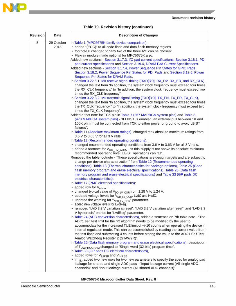
Document revision history
MPC5675K Microcontroller Data Sheet, Rev. 8
Freescale Semiconductor 145
8 29 October 2013
In Table 1 (MPC5675K family device comparison): • added “(ECC)” to all code flash and data flash memory regions. • footnote 6 changed to “any two of the three I2C can be chosen”. • Flexray module made optional for MPC5675K also.Added new sections - Section 3.17.3, I/O pad current specifications, Section 3.18.1, PDI
pad current specifications and Section 3.19.4, DRAM Pad Current Specifications.Added new sections - Section 3.17.4, Power Sequence Pin States for GPIO Pads,
Section 3.18.2, Power Sequence Pin States for PDI Pads and Section 3.19.5, Power Sequence Pin States for DRAM Pads.
In Section 3.22.8.1, MII receive signal timing (RXD[3:0], RX_DV, RX_ER, and RX_CLK), changed the text from “In addition, the system clock frequency must exceed four times the RX_CLK frequency.” to “In addition, the system clock frequency must exceed two times the RX_CLK frequency”.
In Section 3.22.8.2, MII transmit signal timing (TXD[3:0], TX_EN, TX_ER, TX_CLK), changed the text from “In addition, the system clock frequency must exceed four times the TX_CLK frequency.” to “In addition, the system clock frequency must exceed two times the TX_CLK frequency”.
Added a foot note for TCK pin in Table 7 (257 MAPBGA system pins) and Table 8 (473 MAPBGA system pins) - “If LBIST is enabled, an external pull between 1K and 100K ohm must be connected from TCK to either power or ground to avoid LBIST failures”.
In Table 11 (Absolute maximum ratings), changed max absolute maximum ratings from 3.6 V to 3.63 V for all 3 V rails.
In Table 12 (Recommended operating conditions), • changed recommended operating conditions from 3.6 V to 3.63 V for all 3 V rails. • added a footnote for VDD_HV_ADRx - “If this supply is not above its absolute minimum
recommended operating level, LBIST operations can fail”.Removed the table footnote - “These specifications are design targets and are subject to
change per device characterization” from Table 12 (Recommended operating conditions), Table 13 (Thermal characteristics for package options), Table 25 (Code flash memory program and erase electrical specifications), Table 26 (Data flash memory program and erase electrical specifications) and Table 33 (GP pads DC electrical characteristics).
In Table 17 (PMC electrical specifications): • added row for Vadctol. • changed typical value of VDD_LV_COR from 1.28 V to 1.24 V. • updated voltage levels for VDD_LV_COR, LvdC and HvdC. • updated the wording for “VDD_LV_COR” parameter. • added new voltage levels for LvdReg. • removed “LVD 3.3 V variation at reset”, “LVD 3.3 V variation after reset”, and “LVD 3.3
V hysteresis” entries for “LvdReg” parameter.In Table 24 (ADC conversion characteristics), added a sentence on 7th table note - “The
ADC1 self test limit for the S2 algorithm needs to be modified by the user to accommodate for the increased TUE limit of +/-10 counts when operating the device in internal regulation mode. This can be accomplished by reading the current value from the test flash and subtracting 4 counts before storing the value to the ADC1 Self Test Analog Watchdog Register 2 (STAW2R)”.
In Table 26 (Data flash memory program and erase electrical specifications), description of TDWPROGRAM changed to “Single word (32 bits) program time”.
In Table 33 (GP pads DC electrical characteristics), • added rows for VILRSB and VIHRSB. • in IIL, added two new rows for two new parameters to specify the spec for analog pad
leakage for shared and single ADC pads - “Input leakage current (All single ADC channels)” and “Input leakage current (All shared ADC channels)”.
Table 79. Revision history (continued)
Revision Date Description of Changes

MPC5675K Microcontroller Data Sheet, Rev. 8
Document revision history
Freescale Semiconductor146
Revision Date Description of Changes
8 (Contd..) 29 October 2013 In Table 58 (RESET sequences), changed min values of TDRB and TERLB from 60 to 50 ms and typ values from 65 to 60 ms.
In Table 62 (JTAG pin AC electrical characteristics), updated the footnote to - “fTCK = 1/tTCK. fTCK must not exceed 1/4 the frequency of the system clock (SYS_CLK).”
Reverted the first term of Equation 11.

Document Number: MPC5675KRev. 810/2013
Information in this document is provided solely to enable system and software
implementers to use Freescale products. There are no express or implied copyright
licenses granted hereunder to design or fabricate any integrated circuits based on the
information in this document.
Freescale reserves the right to make changes without further notice to any products
herein. Freescale makes no warranty, representation, or guarantee regarding the
suitability of its products for any particular purpose, nor does Freescale assume any
liability arising out of the application or use of any product or circuit, and specifically
disclaims any and all liability, including without limitation consequential or incidental
damages. “Typical” parameters that may be provided in Freescale data sheets and/or
specifications can and do vary in different applications, and actual performance may
vary over time. All operating parameters, including “typicals,” must be validated for
each customer application by customer’s technical experts. Freescale does not convey
any license under its patent rights nor the rights of others. Freescale sells products
pursuant to standard terms and conditions of sale, which can be found at the following
address: http://www.reg.net/v2/webservices/Freescale/Docs/TermsandConditions.htm
How to Reach Us:
Home Page: freescale.com
Web Support: freescale.com/support
Freescale, the Freescale logo, AltiVec, C-5, CodeTest, CodeWarrior, ColdFire,
C-Ware, Energy Efficient Solutions logo, Kinetis, mobileGT, PowerQUICC, Processor
Expert, QorIQ, Qorivva, StarCore, Symphony, and VortiQa are trademarks of
Freescale Semiconductor, Inc., Reg. U.S. Pat. & Tm. Off. Airfast, BeeKit, BeeStack,
ColdFire+, CoreNet, Flexis, MagniV, MXC, Platform in a Package, QorIQ Qonverge,
QUICC Engine, Ready Play, SafeAssure, SMARTMOS, TurboLink, Vybrid, and Xtrinsic
are trademarks of Freescale Semiconductor, Inc. All other product or service names
are the property of their respective owners. The Power Architecture and
Power.org word marks and the Power and Power.org logos and related
marks are trademarks and service marks licensed by Power.org.
© 2009–2013 Freescale Semiconductor, Inc.