QHE Report
25
Quantum Hall Effect in Polar Oxide Heterostructures Amit Kumar Das A reading course undertaken for the requirement of PhD in Homi Bhava National Institute Supervisor: Dr. L. M. Kukre ja Raja Ramanna Center for Advanced Technology Indore 1
-
Upload
amit-kr-das -
Category
Documents
-
view
218 -
download
0
Transcript of QHE Report

8/8/2019 QHE Report
http://slidepdf.com/reader/full/qhe-report 1/25
Quantum Hall Effect in Polar OxideHeterostructures
Amit Kumar Das
A reading course undertaken for the requirement of PhD in Homi Bhava National Institute
Supervisor:
Dr. L. M. Kukreja
Raja Ramanna Center for Advanced TechnologyIndore
1

8/8/2019 QHE Report
http://slidepdf.com/reader/full/qhe-report 2/25
QHE in Polar Oxide Heterostructure Amit Kr Das
Contents
1 Introduction 3
2 The Classical Hall Effect 32.1 Motion of 2D Electrons in Magnetic Field - The Resistivity and
Conductivity Tensors . . . . . . . . . . . . . . . . . . . . . . . . . . 42.2 Resistance and Resistivity in 2D . . . . . . . . . . . . . . . . . . . . 62.3 Subhnikov-de Hass (S-dH) Oscillation - influence of the Quantum
Mechanics on Classical Hall Effect . . . . . . . . . . . . . . . . . . . 6
3 Quantum Hall Effect 83.1 Quantum mechanical treatment of 2D electrons . . . . . . . . . . . 93.2 2D electrons in magnetic field - Landau Quantization . . . . . . . . 103.3 Degeneracy of Landau Levels . . . . . . . . . . . . . . . . . . . . . 123.4 Integer Quantum Hall Effect (IQHE) . . . . . . . . . . . . . . . . . 133.5 Localization effect . . . . . . . . . . . . . . . . . . . . . . . . . . . . 15
4 Experimental 2D electron gas systems 174.1 Metal Oxide Semiconductor Field Effect Transistors (MOSFETs) . 174.2 Semiconductor Heterostructures . . . . . . . . . . . . . . . . . . . . 18
5 Quantum Hall effect in Polar Semiconductors 195.1 High Mobility 2DEG in ZnO . . . . . . . . . . . . . . . . . . . . . . 19
5.2 Subhnikov-de Hass Oscillation and Qunatum Hall Effectin ZnO/MgZnO Heterostructures . . . . . . . . . . . . . . . . . . . 22
6 Our Own Efforts 24
References 24*
2

8/8/2019 QHE Report
http://slidepdf.com/reader/full/qhe-report 3/25
QHE in Polar Oxide Heterostructure Amit Kr Das
1 Introduction
The quantum Hall effect is a quantum-mechanical counterpart of the well known
Hall effect, observed in two-dimensional electron gas (2-DEG) subjected to lowtemperatures and strong perpendicular magnetic fields, in which the Hall conduc-tivity takes on quantized values. The integer quantization of the Hall conductancewas originally predicted by Ando, Matsumoto, and Uemura [1] in 1975, on the ba-sis of an approximate calculation which they themselves did not believe to be true.Several workers subsequently observed the effect in experiments carried out on theinversion layer of MOSFETs. It was only in 1980 that Klaus von Klitzing, workingwith Si/SiO2 based MOSFET samples developed by Michael Pepper and GerhardDorda, made the discovery that the Hall conductivity was exactly quantized [2].For this finding, von Klitzing was awarded the 1985 Nobel Prize in Physics.
Quantum Hall physics – the study of two-dimensional (2D) electrons in a strongperpendicular magnetic field – has become an extremely important research sub- ject during the last two and a half decades. The interest for quantum Hall physicsstems from its position at the borderline between low-dimensional quantum sys-tems and systems with strong electronic correlations, probably the major issues of modern condensed-matter physics. From a theoretical point of view, the study of quantum Hall systems required the elaboration of novel concepts some of whichwere better known in quantum-field theories used in high-energy rather than incondensed-matter physics, such e.g. charge fractionalisation, non-commutativegeometries and topological field theories [3].
Early results in quantum Hall effect (QHE) were obtained in the inversion layerof Si/SiO2 based MOSFET structures [2]. Later on the experiments were success-fully extended to GaAS/AlGaAs interface quantum wells [4]. After the discoveryof fractional QHE, variety of other material systems such as III-nitrides [5] andgraphene [6] has been studied extensively. However the polar II-VI oxides semi-conductors such as ZnO have been elusive in these regards for long. Only recently, in 2007, the first report on QHE in ZnO/MgZnO heterostructure were reportedby Tsukazaki et al [7]. Subsequently another report by Tampo et al appeared in2008 [8] for the same system. However the mechanism of 2-DEG formation andthe source of electrons at the interface of such materials having spontaneous andpiezoelectric polarization is still not well understood. In this reading course first
the basics of 2D electron gas (2DEG) system in strong perpendicular magneticfield will be studied and then a review of the literatures available about 2DEGsystem and QHE in ZnO will be done.
2 The Classical Hall Effect
The classical Hall effect was discovered in 1879 by Edwin Herbert Hall at JohnsHopkins University. The classical Hall effect is the production of a voltage dif-ference (the Hall voltage) across an electrical conductor, transverse to an electriccurrent in the conductor and a magnetic field perpendicular to the current.TheHall system basically consist of a 2D electron gas in a perpendicular magneticfield. To observe the Hall effect, electrical transport measurement is done on such
3

8/8/2019 QHE Report
http://slidepdf.com/reader/full/qhe-report 4/25
QHE in Polar Oxide Heterostructure Amit Kr Das
a system by driving a current I along the length of the system perpendicularto the magnetic field direction and by measuring both the longitudinal and thetransverse resistance (also called Hall resistance). The difference between these
two resistances is essential and can be defined topologically: let us consider acurrent that is driven through the sample via two arbitrary contacts [C1 and C4in Fig.1(a)] and let us draw an imaginary line between these two contacts. Alongitudinal resistance is a resistance measured between two (other) contacts (C5and C6) that may be connected by a line that does not cross the line connectingC1 and C4. The transverse resistance is measured between two contacts that areconnected by an imaginary line that necessarily crosses the line connecting C1 andC4 [e.g. C3 and C5 in Fig.1(a)]. The Hall resistance varies linearly with magneticfield (B) as given by the following equation,
RH = Ben2D
(1)
where e is the charge of the carriers and n2D is the 2D electron density. The figure1(b) shows the variation of Hall resistance with magnetic field. To understandthese behavior of the Hall resistance we need to consider the tensor characteristicsof the resistivity.
Figure 1: (a) 2D electrons in a perpendicular magnetic field (Hall system).In a typical transport measurement, a current I is driven through
the system via the contacts C1 and C4. The longitudinal re-sistance may be measured between the contacts C5 and C6 (oralternatively between C2 and C3). The transverse (or Hall) re-sistance is measured, e.g., between the contacts C3 and C5. (b)Classical Hall resistance as a function of the magnetic field.
2.1 Motion of 2D Electrons in Magnetic Field - The Resistivity andConductivity Tensors
The classical Hall effect and the tensor natures of resistivity and conductivity of
a 2D electron system in a perpendicular magnetic field can be explained with thehelp of Drude’s free electron theory. According to this theory the equation of
4

8/8/2019 QHE Report
http://slidepdf.com/reader/full/qhe-report 5/25
QHE in Polar Oxide Heterostructure Amit Kr Das
motion of a single free electron is given by
dp
dt= −e(E +
p
me
× B) −p
τ (2)
where −e is the electronic charge, E is the applied electric field, p is the momentumof the electron and me is the effective mass of the electrons. The last term takesinto account the relaxation process of the electrons due to collision with impuritiescharacterized by the relaxation time τ . The macroscopic transport characteristics,i.e. the resistivity or conductivity of the system, are obtained from the staticsolution of the equation of motion, i.e. for dp
dt= 0. Moreover for 2D electrons
p = ( px, py, 0). Therefore in steady state from equation (2),
eτ E = −eτ
me
( p × B) − p (3)
Since we are interested in the study of motion of 2D electrons in a perpendicularmagnetic field, we take B = (0, 0, B) and E = (E x, E y, 0). With this the equation(3) can be broken into components as follows,
σ0E x = −en2D pxme
− en2D(ωC τ )pyme
(4)
σ0E y = +en2D(ωC τ )pxme
− en2D pyme
(5)
where ωC =eB
me is a characteristic frequency of the 2D electron system called thecyclotron frequency of the electrons because it arises due to the cyclotron motionof the electrons in the magnetic field. σ0 = n2De
2τ me
is called the Drude conductivity.Now the current density is given by
j = −en2Dp
me
, (6)
Using j, the equations (3) and (4) can be written in a matrix form E = ρ j withthe help of the resistivity tensor ρ, given by,
ρ =
1
σ0
1 ωC τ −ωC τ 1
=
1
σ0
1 µB−µB 1
=ρxx ρxy
ρyx ρyy
(7)
where µ = eτ me
is the mobility of the electrons. The conductivity is defined in thematrix form as j = σE. Therefore the conductivity tensor can be obtained formthe resistivity tensor by simply matrix inversion and it is given by,
σ = ρ−1 =
σxx σxyσyx σyy
(8)
where σxx = σyy = σ01+ω2
Cτ 2
and σyx = −σxy = σ0ωCτ
1+ω2Cτ 2
. The diagonal components
of the resistivity tensor are the longitudinal resistivity and the off-diagonal com-ponents are called the transverse or Hall resistivity. From the equation (6) it is
5

8/8/2019 QHE Report
http://slidepdf.com/reader/full/qhe-report 6/25
QHE in Polar Oxide Heterostructure Amit Kr Das
immediately obvious that the longitudinal resistivity ρxx = ρyy = 1/σ0 and thetransverse resistivity or Hall resistivity ρxy is given by,
ρxy = ωC τ σ0= eBme
τ × men2De2τ = Ben2D
. (9)
It shows that the Hall resistivity is linearly proportional to the magnetic field.Further if we consider the situation of perfect periodic structure with vanishingimpurities so that the relaxation time is very long implying τ >> ω−1C or ωC τ → ∞,the resistivity and the conductivity tensors read as,
ρ =
0 B
en2D
− Ben2D
0
(10)
and
σ = 0 − en2D
Ben2DB
0
(11)
as in this limit σ0 → ∞. So if the tensor nature of the resistivity and conductivityare not taken into account, we reach to the counter-intuitive conclusion that thelongitudinal resistivity and the longitudinal conductivity both vanish simultane-ously. This shows the significance of considering tensor nature of resistivity andconductivity. Therefore the transport properties in the clean limit and in presenceof a magnetic field i.e. ωC τ → ∞ is completely governed by the off-diagonal orthe transverse components of the resistivity and conductivity.
2.2 Resistance and Resistivity in 2DIn the above discussions what we calculated is the resistivity, but in real exper-iments the quantity that is directly measured is the resistance. In general theresistivity and the resistance are related by the formula R = ρL
A, where L is the
length of the conductor and A is the cross section. From the scaling point of view for a d-dimensional conductor, the cross section scales as Ld−1, such that theresistance and resistivity are related by,
R = ρL2−d. (12)
Therefor from the above equation it is obvious that for 2D conductor resistance
and resistivity are same from the dimensional point of view. This scaling argumentneglects the fact that the length L and the width W (the 2D cross section) do notnecessarily coincide; indeed, the resistance of a 2D conductor depends in general onthe so-called scaling factor that is a function of L
A. However for the transverse or
the Hall resistance the length of the conductor itself plays the role of cross sectionso that the scaling factor = 1 and the Hall resistance and the Hall resistivity trulycoincide.
2.3 Subhnikov-de Hass (S-dH) Oscillation - influence of the QuantumMechanics on Classical Hall Effect
A first indication of the influence of quantum phenomena in the transport mea-surement of a 2D electron system in presence of a magnetic field came in 1930 with
6

8/8/2019 QHE Report
http://slidepdf.com/reader/full/qhe-report 7/25
QHE in Polar Oxide Heterostructure Amit Kr Das
the discovery of Subhnikov-de Hass oscillation in the longitudinal resistivity withchanging magnetic field [9]. Whereas the classical resistivity tensor reveals thatthe longitudinal component of resistivity of a 2D electron system in a magnetic
field should be independent of the magnetic field, Subhnikov and de-Hass in con-trast found that beyond a characteristic magnetic field the longitudinal resistivityoscillates with increasing magnetic field. This is schematically shown in figure2(a). The Hall resistance however remains linear in B.
Figure 2: (a) Sketch of the Shubnikov-de Haas effect. Above a critical fieldBc, the longitudinal resistance Rxx starts to oscillate as a functionof the magnetic field. (b) Density of states of 2DEG in normal Bfield (DOS). In a clean system, the DOS consists of equidistantdelta peaks (shaded) at energies n = hωC (n + 1/2), whereas ina sample with a stronger impurity concentration, the peaks arebroadened (dashed lines). The continuous black line representsthe sum of overlapping peaks, and E F denotes the Fermi energy.
The Shubnikov-de Haas oscillation is a consequence of the energy quantizationof the 2D electron in a strong magnetic field, as it has been shown by Landau
at roughly the same moment [10]. In brief, Landau quantization consists of thequantization of the cyclotron radius, i.e. the radius of the circular trajectory of an electron in a magnetic field. As a consequence this leads to the quantisationof its kinetic energy into so-called Landau levels (LLs), n = hωC (n + 1/2), wheren is an integer. In order for this quantisation to be relevant, the magnetic fieldmust be so strong that the electron performs at least one complete circular periodwithout any collision, i.e. ωC τ > 1. This condition defines the critical magneticfield Bc gievn by,
Bc =me
eτ = µ−1 (13)
above which the longitudinal resistivity starts to oscillates with magnetic field.To understand the S-dH oscillation we need to consider the Boltzmann transport
7

8/8/2019 QHE Report
http://slidepdf.com/reader/full/qhe-report 8/25
QHE in Polar Oxide Heterostructure Amit Kr Das
equation which gives that the longitudinal conductivity is given by [3],
σxx = e2Dρ(E F ) (14)
where D is the diffusion co-efficient and ρ(E F ) is the density of states (DOS) atthe Fermi surface. Now due to Landau quantization, the DOS of a clean systemconsist of a sequence of delta peaks at the energies n = hωC (n + 1/2). Thereforethe DOS is given by,
ρ() =n
gnδ( − n) (15)
where gn takes into account the degeneracy of the energy levels. These deltafunction peaks are actually broadened in real samples due to dirt and disorderand may even overlap with each other such that the DOS oscillates in energy with
maxima at the positions of the peaks and minima in between them as shown infigure 2(b) . If the number of electrons in the sample is fixed then the Fermi energyis also fixed. Now if the magnetic field is sweeped, the spacing between the LLsalso change. When the DOS coincides with the Fermi energy, it gets its maximumvalue and when the Fermi energy lies in between two LLs, the DOS is minimum.The resulting oscillation of the DOS and hence of the longitudinal conductivity σxxvia the relation (14) with sweeping magnetic field is the essence of Subhnikov-deHass oscillation.
3 Quantum Hall Effect
At low temperature and sufficiently high magnetic field the Hall resistance is nolonger linear in B; instead it is quantized. It consists of plateaus at certain valuesof magnetic field. In the plateaus, the value of Hall resistance (RH ) is independentof sample parameters and is completely given in terms of universal constants asfollows [2],
RH =
h
e2
1
n, (16)
where n is an integer. The plateau in the Hall resistance is accompanied by a van-ishing longitudinal resistance. This phenomenon is know as the integer quantum
Hall effect (IQHE). This is at first sight reminiscent of the Shubnikov-de Haaseffect, where the longitudinal resistance also reveals minima although it nevervanished. The vanishing of the longitudinal resistance at the Shubnikov-de Haasminima may indeed be used to determine the crossover from the Shubnikov-deHaas regime to the Integer Quantum Hall Effect. This quantization of the Hallresistance is an universal phenomenon i.e. independent of the particular propertiesof the sample, such as its geometry, the host materials used to fabricate the 2Delectron gas and, even more importantly, its impurity concentration or distribu-tion. This universality is the reason of the enormous precision of the Hall resistancequantization ( 10−9). Since 1990 it is being used as the resistant standard,
RK −90 =h
e2= 25812.807Ω, (17)
8

8/8/2019 QHE Report
http://slidepdf.com/reader/full/qhe-report 9/25
QHE in Polar Oxide Heterostructure Amit Kr Das
which is called the Klitzing constant as a respect to the discoverer of IQHE. Furtherthe vanishing of the longitudinal resistance at the plateaus implies infinitely longscattering times in IHQE. This is another indication of the universality of the effect,
i.e. IHQE does not depend on the particular impurity or scatterer arrangements.
3.1 Quantum mechanical treatment of 2D electrons
The Hamiltonian (H ) of a free particle is simply p2
2m, where p and m are respectively
momentum and mass of the particle. In quantum mechanics the obseravbles arerepresented by operators. The operator for momentum (p) is −ih and the timeindependent Schrodinger equation for free electrons is given by [10]
Hψ = Eψ (18)
or
−h2
2m2ψ = Eψ, (19)
E being the energy of the particle. This equation does not contain explicitly x,y or z co-ordinates. Therefore the corresponding components of momentum areconstants of motion and the solution is of the form
ψ = Ceih( pxx+ pyy+ipzz) (20)
Energy of such electrons is simply given by,
E = p
2
x2m + p
2
y2m + p
2
z2m (21)
In case of 2D electrons in the X − Y plane, the motion along the z axis is confinedby lets say the confinement potential V (z). In this case the time independentSchrodinger equation is
−h2
2m
∂ 2
∂x2+
∂ 2
∂y2+
∂ 2
∂z2
ψ + V (z)ψ = Eψ (22)
This time the equation does not contain x and y explicitly, but it has explicitdependence on z. So the solution can be taken as,
ψ = Ceih( pxx+ pyy)φ(z) (23)
Putting this in equation (22), we can get after differentiating appropriately,
−h2
2m
d2φ
dz2+ V (z)φ = E 1φ (24)
E 1 =
E −
p2x2m
− p2y2m
(25)
E 1 is the energy due to confinement along z axis. Now if we consider that theconfinement potential along the z axis is parabolic having the following form
V (z) =1
2mω2z2 (26)
9

8/8/2019 QHE Report
http://slidepdf.com/reader/full/qhe-report 10/25
QHE in Polar Oxide Heterostructure Amit Kr Das
Then equation (24) becomes the equation for a quantum harmonic oscillator withfrequency ω having the following equation,
− h2
2md2φdz2
+ 12
mω2z2φ = E 1φ (27)
And from our knowledge of quantum harmonic oscillator we know that E 1 isquantized having the following values of energy,
E 1 = hω
n +
1
2
, (28)
n being an integer including 0. So from equation (25) the total energy E of theparticle is given by
E =
E 1 +
p2x2m
+ p2y2m
= hω
n +
1
2
+
p2x2m
+ p2y2m
(29)
This equation tells us that the particles behave as free particles in the X − Y plane and for motion along z direction, its energy is quantized with energy levelsseparated by hω having a ground state energy of 1
2hω. However if a magnetic
field is applied along the z axis, the motion in X − Y plane also gets quantized astreated below.
3.2 2D electrons in magnetic field - Landau Quantization
In presence of a magnetic field B, the the momentum operator p is replaced by(p − eA) [10], where e is the charge of the particle and A is the magnetic vectorpotential related to the magnetic field B via the relation,
B = × A (30)
So for 2D electrons in a magnetic field the Schrodinger equation, considering thatits charge is negative, will be,
1
2m(−ih + eA)2 ψ + V (z)ψ = Eψ (31)
The magnetic field is along z axis, so the motion along z axis is not affected by themagnetic field. Further from the previous section we find that for an appropriateconfining potential V (z) along the z direction, particle’s energy due to z motionis quantized; if the temperature is so low that the thermal energy kBT is less thanthe spacing between the quantized energy levels due to z confinement, the motionalong z direction can be safely neglected. In such a case the Schrodinger equationcan be written in the following form,
1
2m(−ih∂ xx − ih∂ yy + eA)2 ψ = E pψ (32)
x and y are the unit vectors along x and y directions respectively and E p is theenergy of the particle for motion in X − Y plane alone. E p is related to E by
10

8/8/2019 QHE Report
http://slidepdf.com/reader/full/qhe-report 11/25
QHE in Polar Oxide Heterostructure Amit Kr Das
the relation E = E p + E 1, E 1 being the quantization energy due to the confiningpotential along z axis. Since the applied magnetic field is along the z direction,we can take A = (−By, 0, 0). This is the so called Landau gauge. With this gauge
the equation (32) can be written as,
1
2m(−ih∂ xx − ih∂ yy − eByx)2 ψ = E pψ (33)
This equation can be further simplified taking the dot product of the vectors intothe following equation
1
2m
−ih∂ 2x − ih∂ 2y + e2B2y2 + 2ieBhy∂ x
ψ = E pψ (34)
Since equation (34) does not contain x explicitly, px is a constant of motion (i.e.a good quantum number) and the solution can be taken as
ψ = Ceih pxxξ(y) (35)
Taking partial derivatives of ψ appropriate number of times w.r.t. x and y andputting in (34), we get
−h2
2m
d2ξ
dy2+
e2B2
2m
y2 − 2y
pxeB
+p2x
e2B2
ξ = E pξ (36)
This equation can be further simplified in the following way
−h2
2m
d2ξ
dy2+
e2B2
2m
y −
pxeB
2ξ = E pξ (37)
or
−h2
2m
d2ξ
dy2+
1
2mω2
C
y −
pxmωC
2
ξ = E pξ (38)
where we have usedωC = eB/m (39)
Equation (38) is the equation of a quantum harmonic oscillator with mass m and
frequency ωC . Therefore we can say that in a normal magnetic field and at lowtemperature the electrons undergo oscillatory motion in the X − Y plane. This isthe so called cyclotron motion of the electrons. The equation also tells that theposition of the center of the cyclotron oscillation depends on px and is given by
y0 =pxeB
=px
mωC
(40)
As seen in the previous section the energy E p of such a quantum oscillator isquantized and is given by [10]
E p = hωC
m + 1
2
, (41)
11

8/8/2019 QHE Report
http://slidepdf.com/reader/full/qhe-report 12/25
QHE in Polar Oxide Heterostructure Amit Kr Das
m being an integer including 0. The total energy spectrum including the compo-nent connected with the z direction motion using relation (28) and (41) is:
E = E 1 + E p = hω
n + 12
+ hωC
m + 12
(42)
As a result the radius of cyclotron motion is also quantized i.e. it can not haveany arbitrary values as in the classical limit. This quantization of the cyclotronradius and the energy of 2D electrons in a strong perpendicular magnetic fieldand at low temperature is called the Landau quantization and the correspondingenergy levels are called Landau Levels (LLs). Because of this Landau quantizationthe density of states (DOS) of 2D electron gas in a strong perpendicular magneticfield contains a series of delta peaks at the positions of the LLs. It is surprising
that a purely discrete energy spectrum which is typical of microscopic objects such
as atoms arises in macroscopic samples.
3.3 Degeneracy of Landau Levels
From equation (38) and (41) in the preceding section, it is obvious that the motionin the x − y plane is described by the two quantum numbers - the discrete LLnumber m and the momentum component px or the y co-ordinate of the oscillatorcenter which is proportional to px. However the energy depends only on m. Thisimplies that the LLs are degenerate over the oscillator position. This is logicalsince the system is uniform in x − y plane and any shift in oscillator position inthis plane must not change the energy of the oscillator.
To calculate the Landau level degeneracy [3] let us assume that Lx and Ly arethe dimensions of the system along the x and y directions respectively. To nullifythe effect of boundary on the system let us assume the periodic boundary conditionψ(x) = ψ(x + Lx). Then from equation (35), px is only allowed to have values2N πh/Lx, N is an integer. So in a momentum interval ∆ px the number of allowedvalues of px is given by ∆ pxLx/2πh. On the other hand the other requirement isthat the oscillator center must lie within the sample i.e.
0 < y0 =pxeB
< Ly (43)
So the total interval of possible values of px i.e. ∆ px is eBLy. Therefore the number
of possible values of px i.e. the Landau level degeneracy iseBLyLx2πh
. Since LxLy
is the area, the Landau level degeneracy per unit area is given by
η =eB
2πh=
1
2πλ2(44)
where λ =
heB
is called the magnetic length. Since λ is the characteristic size of an
electron orbit for the ground state of Landau oscillation, η is the number of electronorbits which can be allocated per unit area without considerable overlapping. Forour convenience we define a quantity ν called the filling factor as the number of LLs which are completely filled by electrons at T = 0. It is given by
ν =n2D
η=
2πhn2D
eB(45)
12

8/8/2019 QHE Report
http://slidepdf.com/reader/full/qhe-report 13/25
QHE in Polar Oxide Heterostructure Amit Kr Das
Figure 3 shows how the Landau levels shift with increasing magnetic field relativeto the Fermi level. 3(a) and 3(b) correspond to integer filling factor ν .
Figure 3:
DOS in presence and absence of magnetic field. In the absence of magnetic field the density of states in 2D is constant as a functionof energy, but in field the available states clump into Landau levelsseparated by the cyclotron energy, with regions of energy betweenthe LLs where there are no allowed states. As the magnetic fieldis swept the LLs move relative to the Fermi energy.
In the above discussion we have not considered spin degeneracy of the Landaulevels. Actual degeneracy will be doubled if both spin states of the electrons areconsidered. And if the Zeemann splitting of the spin degenerate levels is of theorder of orbital Landau level splitting, then the actual number of Landau levels
will be doubled.
3.4 Integer Quantum Hall Effect (IQHE)
The purley quantized spectrum of two-dimensional electron system in a normalmagnetic field at low enough temperature results in a dramatic modification of their transport properties as compared with the three-dimesional case. In thiscase due to the absence of the third degree of freedom, the probability for theelastic scattering of the electrons exhibit giant oscillation with magnetic field. Letus assume that the magnetic field strength is such that the filling factor η is equal
to an integer, lets say N . We also assume that the temperature is so low thatthe thermal energy kBT is less than hωC . In such a case the Fermi level liesbewteen the N -th and (N + 1)-th Landau Levels. All states at all lower N values
13

8/8/2019 QHE Report
http://slidepdf.com/reader/full/qhe-report 14/25
QHE in Polar Oxide Heterostructure Amit Kr Das
Figure 4: Integer quantum Hall effect in a GaAs/GaAlAs heterojunction,recorded at 30mK. The QHE can be seen at liquid helium temper-atures, but in the millikelvin regime the plateaux are much wider.Also included is the diagonal component of resistivity, which showsregions of zero resistance corresponding to each QHE plateau. Inthis figure the plateau index is, from top right, 1, 2, 3, 4, 6, 8....
are completely filled with electrons. Therefore, according to Pauli’s exclusionprinciple, elctron transitions inside these levels are not allowed. Transition to thefree states at higher N values are also not possible since kBT < hωC . Therefore, in
this situation all kinds of scattering events are completely forbidden. This impliesthat the scattering time τ → ∞.
Let us now go back to section 2.1 and look upon the equations (7), (8) and (9).We observe that
ρxx =1
σ0, ρxy =
ωC τ
σ0
(46)
andσxx =
σ0
1 + ω2C τ 2
, |σxy| =σ0ωC τ
1 + ω2C τ 2
(47)
As given earlier σ0 = n2De2τ /me. So for the case discussed in the previous para-graph for integer filling factors, as τ → ∞, ρxx → 0 and σxx → 0. Now for integerfilling factor ν = N , we have from equation (45),
B
n2D
=2πh
eN (48)
Therefore using relations (46) and (48) ρxy will be given by,
ρxy =ωC τ
σ0=
B
en2D=
2πh
e2N (49)
14

8/8/2019 QHE Report
http://slidepdf.com/reader/full/qhe-report 15/25
QHE in Polar Oxide Heterostructure Amit Kr Das
and similarly
σxy =e2N
2πh(50)
Thus for integer filling factors the diagonal component of resistivity vanishes si-
multaneously with the diagonal component of conductivity, whereas the off-diagonal
component of the resistivity as well as that of the conductivity acquires quantized
values expressed in terms of a combination of fundamental constants e and h, com-
pletely independent of sample parametrs, magnetic field, impurity arrangements or
any other factors. Only when the Fermi energy is inside a Landau level, the Hallvoltage changes and a finite value of resistance appears.This is the essence of In-teger Quantum Hall Effect. The figure 4 shows the integer quantum Hall effectin GaAs/AlGaAs heterojunction. The plateaus in ρxy correspond to integer fillingfactors and are indexed ν = 1, 2, 3, 4,.... from the top right corner. Also the oscilla-
tion of the longitudinal component of resistivity ρxx is shown in green. It is evidentthat for integer filling factor i.e. when the off-diagonal or Hall resistivity are inthe plateaus, the longitudinal component of resistivity vanishes in accordance withthe theory discussed above.
Studies have shown that the formulae (49) and (50) are exact and contain nocorrection, that is ρxy is equal to 2πh/e2N to within the accuracy of the mea-surements. This implies that by highly precise Hall resistivity measurements of two-dimensional structure, the quantity e2/h can be found from which precise de-termination of fine structure constant e2/ch can be made as the value of lightvelocity c is known from other experiments. Besides this, the quantity 2πh/e2 has
the dimension of resitance with a numerical value of 25812.807 Ω. As a result2D electron system with well-pronounced quantum Hall platesus can be used asresistance standard.
3.5 Localization effect
It is possible to sweep the Fermi level of the electron system across the Landaulevels keeping the magnetic field constant by varying the 2D electron concentration.In this case also in some concentration interval (∆n2D), σxx vanishes and σxyremains constant. It implies that in this concentration interval the Fermi level isalways fixed in a gap between Landau levels. This is possible only if there are somestates in this gap which can accept ∆n2D electrons without changing the currentthrough the sample. Therefore the sample must contain a reservoir of localizedstates in the gap between the LLs, which can accept electrons and localize themso that they do not contribute to current conduction. Modern physical conceptslink the presence of localized states with the random potential fluctuation in thesample due to inhomogeneous distribution of impurities, dirt and disorder [11].
The general idea of localization of states due to random potential fluctuationwere described by Mott and Anderson. Their idea was that in presence of randomfluctuation of potential, the states near the band edges of materials gets localizedwhile the states at the center of the bands still remains de-localized. This can be
applied in case of 2D electron system also. An ideal 2DEG system in a normalmagnetic field will have delta function density of states as given by equation (42)
15

8/8/2019 QHE Report
http://slidepdf.com/reader/full/qhe-report 16/25
QHE in Polar Oxide Heterostructure Amit Kr Das
and depicted in figure 5(a). In the presence of dirt and disorder i.e. random poten-tial fluctuations, different spatial points become non-equivalent and the electronsenergy in a magnetic field begins to depend on the position of the orbit center
i.e. on px, lifting the degeneracy of Landau levels in the presence. This results inthe broadening of the LLs. Now the states near the edges of the LLs are localizedwhereas those at the center of the LLs are still de-localized. This situations areshown in figure 5(b).
The existance of localized states can explain the appearance of quantum Hallplateaus. As the electron concentration is increased (or the magnetic field is de-creased) in an interval where the Fermi level lies in a region of localized statesbetween the LL peaks, the localized states gradually fill up without any changein the occupation of the de-localized states; thus the Hall resistance does notchange and the longitudinal resistance vanishes (at zero temperature) giving rise
to plateaus in Hall resistance. It is only as the Fermi level passes through the coreof de-localized states that the longitudinal resistance becomes appreciable and theHall resistance makes its transition from one plateau step to the next. Finally, atfinite temperature there is a small longitudinal resistance due to hopping processesbetween localized states at the Fermi level.
Figure 5: Density of states for a two-dimensional system in a normal mag-netic field: (a) the ideal case, (b) the system in presence of randompotential fluctuation. The region containing the localized statesare shaded.
16

8/8/2019 QHE Report
http://slidepdf.com/reader/full/qhe-report 17/25
QHE in Polar Oxide Heterostructure Amit Kr Das
4 Experimental 2D electron gas systems
The history of the quantum Hall effect is intimately related to technological ad-
vances in the fabrication of 2D electron systems with high electronic mobilities.After the first report of quantum Hall effect, which was achieved in the inversionchannel in Si based MOSFET, a lot of progress have been made in semiconductorprocessing. At present other than the MOSFETs, various other possibilities existfor the achievement of 2DEG. Some of the prominent 2D electron gas systems aredetailed below [3].
Figure 6: (a) Schematic of an n-channel MOSFET. S, G, and D are respec-tively source, drain and gate. The band diagrams of the MOSFETin (b) zero applied gate voltage, V G, (c) positive V G and (d) abovethreshold positive V G. In this case a 2DEG is formed at the oxide-semiconductor interface.
4.1 Metal Oxide Semiconductor Field Effect Transistors (MOSFETs)
The schematic and band diagram of a n-channel MOSFET is shown in figure 6. Weassume that the work functions of the metal and the semiconductor (p-type) aresame. As a positive gate voltage V G is applied, the Fermi level in metal is pusheddownward. The electric field pushes the holes in the p-type semiconductor awayfrom the interface and pulls the electrons towards the interface, resulting in thebending of the bands in semiconductor downward. As the positive gate voltage is
increased, there comes a condition when the conduction band in the semiconductoris closer to the Fermi level than the valence band at the interface. On further
17

8/8/2019 QHE Report
http://slidepdf.com/reader/full/qhe-report 18/25
QHE in Polar Oxide Heterostructure Amit Kr Das
increasing the the positive potential of the metal gate beyond a threshold voltage,the bands in semiconductor bend further and the conduction band at the surface of the semiconductor reaches below the Fermi level, resulting in the accumulation of
electrons in the quantum well formed at the semiconductor-oxide interface. Thusa 2DEG is formed at the oxide-semiconductor interface.
Figure 7: Band diagram of AlGaAs/GaAs heterostructure (a) before bandalignment and (b) after band alignment.
4.2 Semiconductor Heterostructures
Semiconductor heterostructure is another very important structure to obtain highquality 2DEG system. It consist of two lattice matched semiconductor layersof different bandgap grown one on the other. For example let us consider theGaAs/AlGaAs system. This is the system where fractional quantum Hall effect wasobserved for the first time. 2DEG mobilities in such systems are very high owingto the high quality of the interfaces, as the layers are grown epitaxially. Figure7 shows the schematic band diagram of a typical GaAs/AlGaAs heterostructure.The bandgap of AlGaAs is larger than that of GaAs. Moreover the AlGaAs layeris n+ doped with some donor up to a certain distance from the interface. Thisdonor doping pins the Fermi level in AlGaAs which is at a higher energy level than
the originally empty conduction band in GaAs. Therefore it becomes energeticallyfavorable for the electrons in donor levels of AlGaAs to occupy the conductionband of GaAs. This charge transfer produces a electric field which bends thebands in AlGaAs upwards and that of GaAs downward. Because of the bandbending a triangular potential well is formed at the interface on the GaAs sidewhere electrons coming from donor level of AlGaAs gets trapped forming a 2Delectron gas system. Since GaAs layer is undoped and the high sheet electronconcentration of the 2DEG effectively screens the scattering coulomb potentialof the impurities in AlGaAs, the mobility in 2DEG is very high (approx. 107
cm2/V-s).
Apart from these two above discussed prominent systems, the other possible2DEG systems are graphene, HEMT etc.
18

8/8/2019 QHE Report
http://slidepdf.com/reader/full/qhe-report 19/25
QHE in Polar Oxide Heterostructure Amit Kr Das
5 Quantum Hall effect in Polar Semiconductors
Wide bandgap semiconductors such as GaN and ZnO are very important from
the point of view of futuristic semiconductor devices. Their large bandgap makesthem suitable candidates for use in high power and high temperature electronicapplications [12]. Further as most of these materials are radiation hard, they arehighly suitable for space applications too. As a virtue of their direct wide bandgap,they are transparent in the visible spectral region and absorbs/emits in the UV-blue spectral region, which enables them to be used in UV detctors, UV emittingdiodes, transparent devices such as thin-film transistors, transparent RAM etc.So a whole branch of electronic devices with novel characteristics, based solely onwide bandgap semiconductors such as GaN or ZnO is possible. In this regard thestudy of 2D electron system in these materials is very important. A high mobility
2D electron system will enable them to be used in high frequency and high powerapplications. And quantum Hall effect is a major tool to study the many aspectsof a 2D electron system [7].
However GaN and ZnO both are polar semiconductors [8] having spontaneouspolarization by virtue of their non-centro-symmetric crystalline structures. Thepolar nature of these materials make them different in many aspects comparedto other non-polar semiconductors such as Si. That is the reason why the firstreport on 2DEG and quantum Hall effect in GaN appeared only in 1992 [5], al-though quantum hall effect was discovered back in 1980 [2]. Khan et al. showedSubhnikov-de Hass (SdH) oscillation and quantum Hall plateaus in GaN/AlGaNheterostructure in 1992. They achieved a room temperature 2DEG mobility of 834 cm2/V-s which increased to 2626 cm2/V-s at 77 K. The first report on SdHoscillations and QHE on ZnO/MgZnO heterostructure came only in 2007 in the journal Science by Tsukazaki et al.[7] However the origin of 2DEG in such sys-tems is still a debated topic and a lot of research is currently going on in thisfield worldwide, not only to observe QHE, but also to achieve the highest mobilityof the 2DEG that is possible. In what follows in the remaining sections, we willdevote our attention solely to the achievements of 2DEG and observation of SdHoscillation and QHE in ZnO/MgZnO heterostructures.
5.1 High Mobility 2DEG in ZnOAs already mentioned in sections 2 and 3, one of the primary requirements forthe observation of Subhnikov-de Hass oscillation and quantum Hall effect is thatτ > ω−1C i.e. the electron should be able to complete one full cyclotron oscillationbefore any kind of scattering events occurs; τ is the scattering time. Now sinceωC = eB/me and mobility µ = eτ/me, where me is the effective mass of electrons,the condition for observing Subhnikov-de Hass oscillation and quantum Hall effectbecomes that B > µ−1. Therefore higher the mobility lower the magnetic fieldrequired for observing SdH oscillations. Not only that, the increasing mobilityallows one to probe the fine structure of the Hall curve and thus to observe those
quantum Hall states which are more fragile, such as some exotic FQHE states.This may be compared to the quest for high resolutions in optics: the higher the
19
8/8/2019 QHE Report
http://slidepdf.com/reader/full/qhe-report 20/25
QHE in Polar Oxide Heterostructure Amit Kr Das
optical resolution, the better the chance of observing tinier objects. In this sense,electronic mobility means resolution and the tiny object is the quantum Hall states[3].
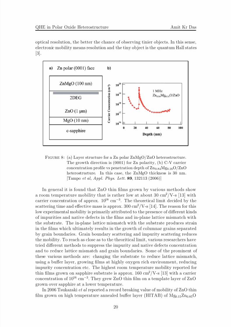
Figure 8: (a) Layer structure for a Zn polar ZnMgO/ZnO heterostructure.The growth direction is (0001) for Zn polarity, (b) C-V carrierconcentration profile vs penetration depth of Zn0.84Mg0.16O/ZnO
heterostructure. In this case, the ZnMgO thickness is 30 nm.[Tampo et al, Appl. Phys. Lett. 89, 132113 (2006)]
In general it is found that ZnO thin films grown by various methods showa room temperature mobility that is rather low at about 30 cm2/V-s [13] withcarrier concentration of approx. 1018 cm−3. The theoretical limit decided by thescattering time and effective mass is approx. 300 cm2/V-s [14]. The reason for thislow experimental mobility is primarily attributed to the presence of different kindsof impurities and native defects in the films and in-plane lattice mismatch withthe substrate. The in-plane lattice mismatch with the substrate produces strain
in the films which ultimately results in the growth of columnar grains separatedby grain boundaries. Grain boundary scattering and impurity scattering reducesthe mobility. To reach as close as to the theoritical limit, various researchers havetried different methods to suppress the impurity and native defects concentrationand to reduce lattice mismatch and grain boundaries. Some of the prominent of these various methods are: changing the substrate to reduce lattice mismatch,using a buffer layer, growing films at highly oxygen rich environment, reducingimpurity concentration etc. The highest room temperature mobility reported forthin films grown on sapphire substrate is approx. 160 cm2/V-s [13] with a carrierconcentration of 1016 cm−3. They grew ZnO thin film on a template layer of ZnO
grown over sapphire at a lower temperature.In 2006 Tsukazaki et al reported a record breaking value of mobility of ZnO thinfilm grown on high temperature annealed buffer layer (HITAB) of Mg0.15Zn0.85O
20

8/8/2019 QHE Report
http://slidepdf.com/reader/full/qhe-report 21/25
QHE in Polar Oxide Heterostructure Amit Kr Das
which itself was grown on ScAlMgO4 (SCAM) substrate [15]. The Mg0.15Zn0.85Olayer was grown on SCAM at 923 K by laser-MBE at oxygen partial pressure of 10−6 Torr. This buffer layer was subsequently annealed at 1273 K in 1 mTorr of
oxygen. On this semi-insulating HITAB, ZnO films were grown at different growthtemperatures and oxygen partial pressure by the same laser-MBE. They reported amaximum room temperature mobility of approx. 440 cm2/V-s which increased to5000 cm2/V-s at 100 K for the film grown at 1250 K at oxygen partial pressure of 10−6 Torr. Residual electron concentration was 9 × 10¹⁵ and 4 × 10¹⁴ at 300 K and100 K respectively. They reasoned that the high electron mobilities are a result of reduction in the ionized impurity scattering. They concluded that as their processwas similar to homoepitaxy, properly treated ZnO single crystals substrate shouldgive same or even better results.
Figure 9: Temperature dependent mobility for Zn polar ZnO and Zn-MgO/ZnO heterostructures. [Tampo et al, Appl. Phys. Lett.
89, 132113 (2006)]
In 2003 Edahiro et al demonstrated 2DEG formation in O-polar ZnO/ZnMnOheterostructure and also showed Subhnikov-de Hass oscillations in magnetoresis-tance measurements [16]. In 2006, Tampo et al reported the formation of 2DEG inZn-polar ZnO/MgZnO heterostructures grown by radical source molecular beamepitaxy [12]. These Zn polar ZnMgO/ZnO heterostructures were grown on c-planesapphire substrates by controlling the thickness of the MgO buffer layer (please re-fer to figure 8(a)). The depth profiling of the carrier concentration as measured byC-V methods is shown in figure 8(b). Electron accumulation at the ZnMgO/ZnOinterface can be seen with concentration of 4 × 1019 cm−3. This implies the for-
mation of 2DEG at the interface. The sheet carrier concentration was found toincrease with Mg concentration. This carrier concentration was one order of mag-nitude higher than that of conventional III-V semiconductor heterostrucuture. The
21

8/8/2019 QHE Report
http://slidepdf.com/reader/full/qhe-report 22/25
QHE in Polar Oxide Heterostructure Amit Kr Das
reason of this high carrier concentration was given as the surface charge induceddue to the strong spontaneous and piezoelecric polarization of ZnO and MgZnOlayers. Further proof of 2DEG formation was given by the temperature dependent
mobility measurements as shown in figures 9 for ZnMgO/ZnO heterostructuresand ZnO thin film. For ZnO thin film mobility decreases rapidly below 100 Kdue to enhancement in ionized impurity scattering whereas the mobility of the Zn-MgO/ZnO heterostructures monotonically increases with deceasing temperaturedue to reduction in ionized impurity scattering, which is especially prevalent at lowtemperature. This reduction in ionized impurity scattering is caused by screen-ing of the impurity scattering potential arising from the high electron density atthe interface. The room temperature mobility of ZnMgO/ZnO heterostructures atroom temperature was 231 cm2/V-s which increased to 2750 cm2/V-s at 4 K.
5.2 Subhnikov-de Hass Oscillation and Qunatum Hall Effectin ZnO/MgZnO Heterostructures
Figure 10: (a) Schematic of the ZnO/MgZnO heterostructures grown onSCAM substrate. (b) Potential diagram near the heterointer-
faces.[Tsukazaki et al, Science 315, 1388 (2007)]
Subhnikov-de Hass oscillation in the longitudinal resistivity and quantum Hallplateaus were observed for the first time in ZnO/MgZnO heterostructures byTsukazaki et al in 2007 [7]. As described earlier in the last subsection they hadgrown ZnO film on high temperature annealed (HITAB) MgZnO relaxed bufferwhich itself was grown on SCAM. They argued that the due to spontaneous andpiezoelectric polarization of the individual layers, polarization induced accumula-tion of surface charges happen at the ZnO side of the interface. The schematicof the structure and the band digram is shown in figure 10. These accumulated
charges at the interface forms the 2DEG. Magnetotransport measurements of thesamples in Hall bar geometry were performed at 45 mK using a standard lock-inamplifier with ac excitation (10nA, 19 Hz). Above a magnetic field of 2 T, SdH
22

8/8/2019 QHE Report
http://slidepdf.com/reader/full/qhe-report 23/25
QHE in Polar Oxide Heterostructure Amit Kr Das
oscillations in longitudinal resistivity component (ρxx) were observed that were pe-riodic in B−1, and the oscillation amplitude increased with increasing B. Althoughthe zero resistance state was absent due to large scattering rate, each minimum
of ρxx coincided with the quantized Hall resistance (ρxy) plateaus equal to h/νe2,where ν is the Landau level filling index. This is shown in figure 11(a).
Figure 11: (a) Longitudinal resistivity ρxx, Hall resistivity ρxy, and differ-ential Hall resistivity dρxy/dB versus B measured at 45 mK (b)Normalized magnetoresistivity versus 1/B recorded at varioustemperatures. Inset depicts temperature dependence of the log-arithmic amplitude of normalized ρxx peak at 3.86 T (indicatedby arrow).[Tsukazaki et al, Science 315, 1388 (2007)]
The 2D carrier density can be calculated from the Fan diagram which is nothingbut a plot of the index of the extrema of ρxx or of dρxy/dB as a function of 1/B.The high field slope of this graph gives the 2D carrier density by the formulan2D = eS H /h, where S H is the high field slope of the plot. The effective mass can
be calculated from the temperature dependence of the normalized SdH oscillationamplitude given by [ρxx(B) − ρxx(0)]/ρxx(0) = A (say), where ρxx(0) is the zerofield value of ρxx. The resulting plot is called the Dingle plot. However for Dingleplot the ρxx(B) data has to be corrected for magnetoresistance. From the slope of the Dingle plot i.e. ln(A/T ) vs. T plot, the effective mass can be extracted usingthe formula
ln
A
T
= C −
2π2mekBeBh
T (51)
The Dingle plot is shown in 11(b). The values of 2D carrier concentration ascalculated by Tsukazaki et al varied from 6 × 10¹¹ to 1.8 × 1012 cm−2. And thevalue of effective mass was evaluated to be approx. 0.32 m0 which is heavier thanthe bulk polaron mass (0.28 m0), giving rise to the possibility of mass enhancement
23

8/8/2019 QHE Report
http://slidepdf.com/reader/full/qhe-report 24/25
QHE in Polar Oxide Heterostructure Amit Kr Das
with 2D polaronic corrections.Tampo et al also reported in 2008 [8] SdH oscillation in Zn polar ZnMgO/ZnO
heterostructures at a temperature of 0.5 K. In their case the 2D carrier concentra-
tion was approx. 6 × 1012 cm−2 at 4 K.
Even with these results there is lots of scope of further research on the quantumHall effect in ZnO/MgZnO heterostructures. For example the origin of 2DEG insuch polar structures is not yet settled. Moreover the possibility of 2DEG baseddevices opens up an excellent are of research.
6 Our Own Efforts
In view of the potential of QHE in ZnO, we have also initiated efforts in thisdirection. As we realize from the theory of quantum Hall effect, it is very importantto achieve high electron mobilities in the ZnO films. One of the major limitingfactor of electron mobilities in ZnO films grown on sapphire are the sacttering bythe grain boundary potential. These grains are mainly created due to in-planelattice mismatch of ZnO with sapphire substrates. To reduce the number of grainsand increase the invidual grain size, we have deviced a novel high temperature twostep buffer assisted growth methodology. This methodology is based on the studythat at high growth temperature of 7500C on sapphire substrate, ZnO grows onthe Oxygen sub-lattice of alumina lattice, which results in less lattice mismatchand less residual strain in the film [17]; these effects culminate in larger grain sizes.So we grow a buffer of ZnO on sapphire substrate at 7500C for approx. 20 nm and
then on this buffer the final ZnO film is grown at a lower temperature. The bufferprovides for a relaxed template layer for the growth of ZnO film. We have seen byHall measurements that if we grow a ZnO film at 5500C on the 7500C grown bufferwe could achieve a room temperature mobility of approximately 80 cm2/V-s. Thisis in contrast to the mobilities (30 cm2/V-s) that are obtained if the film is grownwithout the buffer layer. Further work is currently underway.
References
[1] T. Ando, Y. Matsumoto, and Y. Uemura, “Theory of Hall effect in a two-dimensional electron system,” J. Phys. Soc. Jpn , vol. 39, pp. 279–288, 1975.
[2] K. v. Klitzing, G. Dorda, and M. Pepper, “New method for high-accuracy de-termination of the fine-structure constant based on quantized Hall resistance,”Phys. Rev. Lett., vol. 45, pp. 494–497, 1980.
[3] M. O. Goerbig, “Quantum Hall Effect,” arXive, vol. 0909.1998v2, 2009.
[4] D. C. Tsui and A. C. Gossard, “Resistance standard using quantization of thehall resistance of GaAs/AlGaAs heterostructures,” Appl. Phys. Lett., vol. 38,p. 550, 1981.
[5] M. A. Khan, J. Kunjia, J. M. V. Hove, N. Pan, and J. Carter, “Observationof a two-dimensional electron gas in low pressure metalorganic chemical vapor
24

8/8/2019 QHE Report
http://slidepdf.com/reader/full/qhe-report 25/25
QHE in Polar Oxide Heterostructure Amit Kr Das
deposited GaN/AlGaN heterojunctions,” Appl. Phys. Lett., vol. 60, pp. 3027–3029, 1992.
[6] K. S. Novoselov et al, “Electric field effect in atomically thin carbon films,”Science, vol. 306, p. 666, 2004.
[7] A. Tsukazaki, A. Ohtomo, T. Kita, Y. Ohno, H. Ohno, and M. Kawasaki,“Quantum Hall effect in polar oxide heterostructures,” Science, vol. 315,p. 1388, 2007.
[8] H. Tampo et al, “Polarization-induced two-dimensional electron gases in Zn-MgO/ZnO heterostructures,” Appl. Phys. Lett., vol. 93, p. 202104, 2008.
[9] L. W. Shubnikov and W. J. de Haas Proceedings of the Royal Netherlands
Society of Arts and Science, vol. 33, p. 130 and 163, 1930.
[10] L. D. Landau and E. M. Lifshitz, Quantum Mechanics: Nonrelativistic The-
ory . Pergamon Press, 1977.
[11] A. Shik, Quantum Wells: Physics and electronics of 2-dimensional systems.World Scientific, 1999.
[12] H. Tampo et al, “Two-dimensional electron gas in Zn polar ZnMgO/ZnO het-erostructures grown by radical source molecular beam epitaxy,” Appl. Phys.
Lett., vol. 89, p. 132113, 2006.
[13] E. M. Kaidashev et al, “High electron mobility of epitaxial ZnO thin filmson c-plane sapphire grown by multistep pulsed-laser deposition,” Appl. Phys.
Lett., vol. 82, no. 22, p. 3901, 2003.
[14] J. D. Albrecht, P. P. Ruden, S. Limpijumnong, W. R. L. Lambrecht, , andK. F. Brennan, “High field electron transport properties of bulk ZnO,” J.
Appl. Phys., vol. 86, p. 6864, 1999.
[15] A. Tsukazaki, A. Ohtomo, and M. Kawasaki, “High-mobility electronic trans-port in ZnO thin films,” Appl. Phys. Lett., vol. 88, p. 152106, 2006.
[16] T. Edahiro, N. Fujimura, and T. Ito, “Formation of two-dimensional electrongas and the magnetotransport behavior of ZnMnO/ZnO heterostructure,” J.
Appl. Phys., vol. 93, no. 10, p. 7673, 2003.
[17] P. Misra and L. M. Kukreja, “Buffer-assisted low temperature growth of high crystalline quality ZnO films using Pulsed Laser Deposition,” Thin Solid
Films, vol. 485, pp. 42–46, 2005.