
qadc queued analog-to-digital converter reference manual
122
Motorola reserves the right to make changes without further notice to any products herein. Motorola makes no warranty, representation or guarantee regarding the suitability of its products for any particular purpose, nor does Motorola assume any liability arising out of the application or use of any product or circuit, and specifically disclaims any and all liability, including without limitation consequential or incidental damages. "Typical" parameters can and do vary in different applications. All operating parameters, including "Typicals" must be validated for each customer application by customer's technical experts. Motorola does not convey any license under its patent rights nor the rights of others. Motorola products are not designed, intended, or authorized for use as components in systems intended for surgical implant into the body, or other applications intended to support or sustain life, or for any other application in which the failure of the Motorola product could create a situation where personal injury or death may occur. Should Buyer purchase or use Motorola products for any such unintended or unauthorized application, Buyer shall indemnify and hold Motorola and its officers, employees, subsidiaries, affiliates, and distributors harmless against all claims, costs, damages, and expenses, and reasonable attorney fees arising out of, directly or indirectly, any claim of personal injury or death associated with such unintended or unauthorized use, even if such claim alleges that Motorola was negligent regarding the design or manufacture of the part. MOTOROLA and the Motorola logo are registered trademarks of Motorola, Inc. Motorola, Inc. is an Equal Opportunity/Affirmative Action Employer. © MOTOROLA, INC. 1995, 1996 QADC QUEUED ANALOG-TO-DIGITAL CONVERTER REFERENCE MANUAL Freescale Semiconductor, I Freescale Semiconductor, Inc. For More Information On This Product, Go to: www.freescale.com nc...
Transcript of qadc queued analog-to-digital converter reference manual

Motorola itabilityof its prod ny andall liability cluding"Typicals others.Motorola nded tosupport o d Buyerpurchase idiaries,affiliates, ersonalinjury or d part. MOTOR
Fre
esc
ale
Se
mic
on
du
cto
r, I
Freescale Semiconductor, Inc.n
c..
.
reserves the right to make changes without further notice to any products herein. Motorola makes no warranty, representation or guarantee regarding the suucts for any particular purpose, nor does Motorola assume any liability arising out of the application or use of any product or circuit, and specifically disclaims a, including without limitation consequential or incidental damages. "Typical" parameters can and do vary in different applications. All operating parameters, in" must be validated for each customer application by customer's technical experts. Motorola does not convey any license under its patent rights nor the rights of products are not designed, intended, or authorized for use as components in systems intended for surgical implant into the body, or other applications inter sustain life, or for any other application in which the failure of the Motorola product could create a situation where personal injury or death may occur. Shoul or use Motorola products for any such unintended or unauthorized application, Buyer shall indemnify and hold Motorola and its officers, employees, subs and distributors harmless against all claims, costs, damages, and expenses, and reasonable attorney fees arising out of, directly or indirectly, any claim of peath associated with such unintended or unauthorized use, even if such claim alleges that Motorola was negligent regarding the design or manufacture of the
OLA and the Motorola logo are registered trademarks of Motorola, Inc. Motorola, Inc. is an Equal Opportunity/Affirmative Action Employer.
© MOTOROLA, INC. 1995, 1996
QADCQUEUED ANALOG-TO-DIGITAL
CONVERTERREFERENCE MANUAL
For More Information On This Product,
Go to: www.freescale.com

F
ree
sca
le S
em
ico
nd
uc
tor,
I
Freescale Semiconductor, Inc.n
c..
.
For More Information On This Product,
Go to: www.freescale.com

Fre
esc
ale
Se
mic
on
du
cto
r, I
Freescale Semiconductor, Inc.n
c..
.
PREFACEThis manual describes the capabilities, operation, and functions of the queued analog-to-digital converter (QADC). The following conventions are used throughout the man-ual.
Logic level one is the voltage that corresponds to Boolean true (1) state.
Logic level zero is the voltage that corresponds to Boolean false (0) state.
To set a bit or bits means to establish logic level one on the bit or bits.
To clear a bit or bits means to establish logic level zero on the bit or bits.
A signal that is asserted is in its active logic state. An active low signal changes fromlogic level one to logic level zero when asserted, and an active high signal changesfrom logic level zero to logic level one.
A signal that is negated is in its inactive logic state. An active low signal changes fromlogic level zero to logic level one when negated, and an active high signal changesfrom logic level one to logic level zero.
LSB means least significant bit or bits. MSB means most significant bit or bits. Refer-ences to low and high bytes are spelled out.
A specific bit or signal within a range is referred to by mnemonic and number. Forexample, ADDR15 is bit 15 of the address bus. A range of bits or signals is referredto by mnemonic and the numbers that define the range. For example, DATA[7:0] formthe low byte of the data bus.
QADC PREFACE MOTOROLA
REFERENCE MANUAL iii
For More Information On This Product, Go to: www.freescale.com

Fre
esc
ale
Se
mic
on
du
cto
r, I
Freescale Semiconductor, Inc.n
c..
.
For More Information On This Product, Go to: www.freescale.com

Paragraph Title Page
TABLE OF CONTENTS
F
ree
sca
le S
em
ico
nd
uc
tor,
I
Freescale Semiconductor, Inc.n
c..
.
SECTION 1 OVERVIEW
1.1 Block Diagram ...........................................................................................1-11.2 QADC Features .........................................................................................1-21.3 Memory Map .............................................................................................1-2
SECTION 2 SIGNAL DESCRIPTIONS
2.1 Port A Pin Functions ..................................................................................2-22.1.1 Port A Analog Input Pins ...................................................................2-22.1.2 Port A Digital Input/Output Pins .........................................................2-22.2 Port B Pin Functions ..................................................................................2-22.2.1 Port B Analog Input Pins ...................................................................2-22.2.2 Port B Digital Input Pins ....................................................................2-22.3 External Trigger Input Pins ........................................................................2-32.4 Multiplexed Address Output Pins ..............................................................2-32.5 Multiplexed Analog Input Pins ...................................................................2-32.6 Voltage Reference Pins .............................................................................2-42.7 Dedicated Analog Supply Pins ..................................................................2-42.8 External Digital Supply Pin ........................................................................2-42.9 Internal Digital Supply Pins .......................................................................2-4
SECTION 3 CONFIGURATION AND CONTROL
3.1 QADC Bus Interface Unit ..........................................................................3-13.2 QADC Bus Accessing ...............................................................................3-13.3 Module Configuration ................................................................................3-33.3.1 Low Power Stop Mode ......................................................................3-33.3.2 Freeze Mode .....................................................................................3-43.3.3 Supervisor/Unrestricted Address Space ...........................................3-43.3.4 Interrupt Arbitration Priority ...............................................................3-53.3.5 QADC Module Configuration Register ..............................................3-53.4 QADC Test Register ..................................................................................3-63.5 General-Purpose I/O Port Operation .........................................................3-63.5.1 Port Data Register .............................................................................3-63.5.2 Port Data Direction Register ..............................................................3-7
SECTION 4 EXTERNAL MULTIPLEXING
4.1 External Multiplexing Operation ................................................................4-14.2 Module Version Options ............................................................................4-3
QADC TABLE OF CONTENTS MOTOROLA
REFERENCE MANUAL v
For More Information On This Product, Go to: www.freescale.com

(Continued)Paragraph Title Page
TABLE OF CONTENTS
Fre
esc
ale
Se
mic
on
du
cto
r, I
Freescale Semiconductor, Inc.n
c..
.
SECTION 5 PIN CONNECTION CONSIDERATIONS
5.1 Analog Reference Pins ..............................................................................5-15.2 Analog Power Pins ....................................................................................5-15.3 Analog Supply Filtering and Grounding .....................................................5-35.4 Accommodating Positive/Negative Stress Conditions ...............................5-55.5 Analog Input Considerations .....................................................................5-65.6 Analog Input Pins ......................................................................................5-85.6.1 Settling Time for the External Circuit .................................................5-95.6.2 Error Resulting from Leakage .........................................................5-10
SECTION 6 ANALOG SUBSYSTEM
6.1 Analog-to-Digital Converter Operation ......................................................6-16.1.1 Conversion Cycle Times ...................................................................6-26.1.1.1 Amplifier Bypass Mode Conversion Timing ..............................6-26.2 Front-End Analog Multiplexer ....................................................................6-36.3 Digital to Analog Converter Array ..............................................................6-36.4 Comparator ...............................................................................................6-46.5 Successive Approximation Register ..........................................................6-4
SECTION 7 DIGITAL CONTROL
7.1 Queue Priority ...........................................................................................7-17.2 Boundary Conditions .................................................................................7-37.3 Scan Modes ..............................................................................................7-47.3.1 Disabled Mode and Reserved Mode .................................................7-47.3.2 Single-Scan Modes ...........................................................................7-47.3.2.1 Software Initiated Single-Scan Mode ........................................7-57.3.2.2 External Trigger Single-Scan Mode ..........................................7-67.3.2.3 Interval Timer Single-Scan Mode ..............................................7-67.3.3 Continuous-Scan Modes ...................................................................7-77.3.3.1 Software Initiated Continuous-Scan Mode ................................7-87.3.3.2 External Trigger Continuous-Scan Mode ..................................7-97.3.3.3 Periodic Timer Continuous-Scan Mode ....................................7-97.4 QADC Clock (QCLK) Generation ..............................................................7-97.5 Periodic/Interval Timer ............................................................................7-137.6 Control and Status Registers ..................................................................7-147.6.1 Control Register 0 ...........................................................................7-147.6.2 Control Register 1 ...........................................................................7-167.6.3 Control Register 2 ...........................................................................7-177.6.4 Status Register ................................................................................7-20
MOTOROLA TABLE OF CONTENTS QADC
vi REFERENCE MANUAL
For More Information On This Product, Go to: www.freescale.com
(Continued)Paragraph Title Page
TABLE OF CONTENTS
Fre
esc
ale
Se
mic
on
du
cto
r, I
Freescale Semiconductor, Inc.n
c..
.
7.7 Conversion Command Word Table .........................................................7-267.8 Result Word Table ...................................................................................7-32
SECTION 8 INTERRUPTS
8.1 Interrupt Operation ....................................................................................8-18.2 Polled and Interrupt-Driven Operation .......................................................8-18.3 Interrupt Sources .......................................................................................8-28.4 QADC Interrupt Register ...........................................................................8-28.5 Interrupt Priority .........................................................................................8-38.6 Interrupt Arbitration ....................................................................................8-48.7 Interrupt Vectors ........................................................................................8-48.8 Initializing the QADC for Interrupt Driven Operation .................................8-58.9 Interrupt Processing Summary ..................................................................8-6
SECTION 9 QUEUE PRIORITY EXAMPLES
9.1 Queue Priority Schemes ...........................................................................9-1
APPENDIX A ELECTRICAL CHARACTERISTICS
APPENDIX B REGISTER SUMMARY
B.1 Address Map ............................................................................................ B-1B.2 QADC Registers ....................................................................................... B-1B.2.1 QADC Module Configuration Register ............................................. B-1B.2.2 QADC Test Register ......................................................................... B-2B.2.3 QADC Interrupt Register .................................................................. B-2B.2.4 Port A/B Data Register ..................................................................... B-3B.2.5 Port Data Direction Register ............................................................. B-3B.2.6 QADC Control Registers .................................................................. B-4B.2.7 QADC Status Register ..................................................................... B-7B.2.8 Conversion Command Word Table .................................................. B-8B.2.9 Result Registers ............................................................................. B-11
APPENDIX C CONVERSION ACCURACY DEFINITIONS
C.1 Transfer Curve ......................................................................................... C-1C.2 Offset Error ............................................................................................... C-2C.3 Quantizing Error ....................................................................................... C-2C.4 Monotonicity ............................................................................................. C-2C.5 Gain Error (Slope Error) ........................................................................... C-2C.6 Integral Non-Linearity ............................................................................... C-3
QADC TABLE OF CONTENTS MOTOROLA
REFERENCE MANUAL vii
For More Information On This Product, Go to: www.freescale.com

(Continued)Paragraph Title Page
TABLE OF CONTENTS
Fre
esc
ale
Se
mic
on
du
cto
r, I
Freescale Semiconductor, Inc.n
c..
.
C.7 Differential Non-Linearity (Related to Monotonicity) ................................. C-4
INDEX
MOTOROLA TABLE OF CONTENTS QADC
viii REFERENCE MANUAL
For More Information On This Product, Go to: www.freescale.com

Figure Title Page
LIST OF ILLUSTRATIONS
F
ree
sca
le S
em
ico
nd
uc
tor,
I
Freescale Semiconductor, Inc.n
c..
.
1-1 QADC Block Diagram ..................................................................................... 1-12-1 QADC Input and Output Signals .................................................................... 2-13-1 Bus Cycle Accesses ....................................................................................... 3-24-1 Example of External Multiplexing ................................................................... 4-25-1 Analog Input Circuitry ..................................................................................... 5-25-2 Errors Resulting from Clipping ....................................................................... 5-35-3 Star-Ground at the Point of Power Supply Origin ........................................... 5-45-4 Input Pin Subjected to Negative Stress .......................................................... 5-55-5 Voltage Limiting Diodes in a Negative Stress Circuit ..................................... 5-65-6 External Multiplexing Of Analog Signal Sources ............................................ 5-75-7 Electrical Model of an A/D Input Pin ............................................................... 5-86-1 QADC Module Block Diagram ........................................................................ 6-16-2 Conversion Timing ......................................................................................... 6-26-3 Bypass Mode Conversion Timing ................................................................... 6-37-1 QADC Queue Operation With Pause ............................................................. 7-27-2 QADC Clock Subsystem Functions .............................................................. 7-107-3 QADC Clock Programmability Examples ..................................................... 7-127-4 Queue Status Transition ............................................................................... 7-257-5 QADC Conversion Queue Operation ........................................................... 7-278-1 QADC Interrupt Flow Diagram ....................................................................... 8-18-2 QADC Interrupt Vector Format ....................................................................... 8-59-1 CCW Priority Situation 1 ................................................................................. 9-29-2 CCW Priority Situation 2 ................................................................................. 9-39-3 CCW Priority Situation 3 ................................................................................. 9-39-4 CCW Priority Situation 4 ................................................................................. 9-49-5 CCW Priority Situation 5 ................................................................................. 9-49-6 CCW Priority Situation 6 ................................................................................. 9-59-7 CCW Priority Situation 7 ................................................................................. 9-59-8 CCW Priority Situation 8 ................................................................................. 9-69-9 CCW Priority Situation 9 ................................................................................. 9-69-10 CCW Priority Situation 10 ............................................................................... 9-79-11 CCW Priority Situation 11 ............................................................................... 9-79-12 CCW Freeze Situation 12 ............................................................................... 9-89-13 CCW Freeze Situation 13 ............................................................................... 9-89-14 CCW Freeze Situation 14 ............................................................................... 9-89-15 CCW Freeze Situation 15 ............................................................................... 9-99-16 CCW Freeze Situation 16 ............................................................................... 9-99-17 CCW Freeze Situation 17 ............................................................................... 9-99-18 CCW Freeze Situation 18 ............................................................................... 9-99-19 CCW Freeze Situation 19 ............................................................................. 9-10C-1 Transfer Curve of an Ideal 10-Bit A/D Converter ...........................................C-1
QADC LIST OF ILLUSTRATIONS MOTOROLA
REFERENCE MANUAL ix
For More Information On This Product, Go to: www.freescale.com

(Continued)Figure Title Page
LIST OF ILLUSTRATIONS
Fre
esc
ale
Se
mic
on
du
cto
r, I
Freescale Semiconductor, Inc.n
c..
.
C-2 Transfer Curve of a Non-Monotonic 10-Bit A/D Converter .............................C-2C-3 Transfer Curve of a 10-Bit A/D Converter with Gain Error .............................C-3C-4 Transfer Curve of a 10-Bit A/D Converter With Integral > One LSB ..............C-4C-5 Transfer Curve of a 10-Bit A/D Converter With Differential Linearity .............C-5
MOTOROLA LIST OF ILLUSTRATIONS QADC
x REFERENCE MANUAL
For More Information On This Product, Go to: www.freescale.com
Table Title Page
LIST OF TABLES
F
ree
sca
le S
em
ico
nd
uc
tor,
I
Freescale Semiconductor, Inc.n
c..
.
1-1 QADC Address Map .............................................................................................. 1-32-1 Multiplexed Analog Input Channels ....................................................................... 2-34-1 Analog Input Channels .......................................................................................... 4-35-1 External Circuit Settling Time (10-Bit Conversions).............................................. 5-95-2 Error Resulting From Input Leakage (IOFF) ........................................................ 5-107-1 QADC Clock Programmability ............................................................................. 7-127-2 Prescaler Clock High Times ................................................................................ 7-157-3 Prescaler Clock Low Times ................................................................................. 7-167-4 Queue 1 Operating Modes .................................................................................. 7-177-5 Queue 2 Operating Modes .................................................................................. 7-187-6 Queue Status....................................................................................................... 7-247-7 Input Sample Times............................................................................................. 7-307-8 Nonmultiplexed Channel Assignments and Pin Designations............................. 7-317-9 Multiplexed Channel Assignments and Pin Designations.................................... 7-328-1 QADC Status Flags and Interrupt Sources............................................................ 8-29-1 Trigger Events ....................................................................................................... 9-19-2 Status Bits.............................................................................................................. 9-2A-1 QADC Maximum Ratings ......................................................................................A-1A-2 QADC DC Electrical Characteristics (Operating) ..................................................A-2A-3 QADC AC Electrical Characteristics (Operating) ..................................................A-3A-4 QADC Conversion Characteristics (Operating).....................................................A-4B-1 QADC Address Map..............................................................................................B-1B-2 Prescaler Clock High Times..................................................................................B-4B-3 Prescaler Clock Low Times...................................................................................B-5B-4 Queue 1 Operating Modes....................................................................................B-5B-5 Queue 2 Operating Modes....................................................................................B-6B-6 Queue Status ........................................................................................................B-8B-7 Input Sample Times ..............................................................................................B-9B-8 Nonmultiplexed Channel Assignments and Pin Designations.............................B-10B-9 Multiplexed Channel Assignments and Pin Designations ...................................B-10
QADC LIST OF TABLES MOTOROLA
REFERENCE MANUAL xi
For More Information On This Product, Go to: www.freescale.com

Fre
esc
ale
Se
mic
on
du
cto
r, I
Freescale Semiconductor, Inc.n
c..
.
MOTOROLA LIST OF TABLES QADC
xii REFERENCE MANUAL
For More Information On This Product, Go to: www.freescale.com

Fre
esc
ale
Se
mic
on
du
cto
r, I
Freescale Semiconductor, Inc.n
c..
.
SECTION 1 OVERVIEWThe queued analog-to-digital converter (QADC) is a 10-bit, unipolar, successive ap-proximation converter. A maximum of 16 analog input channels can be supported us-ing internal multiplexing. A maximum of 44 input channels can be supported in theexpanded, externally multiplexed mode. The actual number of channels dependsupon the number of pins available to the QADC module.
1.1 Block Diagram
Figure 1-1 displays the major components of the QADC module. The QADC consistsof an analog front-end and a digital control subsystem, which includes an intermodulebus (IMB) interface block.
Figure 1-1 QADC Block Diagram
The analog section includes input pins, an analog multiplexer, and two sample andhold analog circuits. The analog conversion is performed by the digital-to-analog con-verter (DAC) resistor-capacitor array and a high-gain comparator.
The digital control section contains control logic to sequence the conversion process,channel select logic, and a successive approximation register (SAR). Also includedare the periodic/interval timer, control and status registers, the conversion commandword (CCW) table RAM, and the result word table RAM.
QADC BLOCK
QUEUE OF 10-BIT CONVERSIONCOMMAND WORDS (CCW), 40 WORDS
INTERMODULE BUS INTERFACE
DIGITAL CONTROL
10-BIT RESULT TABLE,40 WORDS
10-BIT TO 16-BITRESULT ALIGNMENT
10-BIT ANALOG TO DIGITAL CONVERTER
ANALOG INPUT MULTIPLEXER ANDDIGITAL PIN FUNCTIONS
EXTERNALTRIGGERS
EXTERNALMUX ADDRESS
UP TO 16 ANALOGINPUT PINS
REFERENCEINPUTS
ANALOG POWERINPUTS
QADC OVERVIEW MOTOROLA
REFERENCE MANUAL 1-1
For More Information On This Product, Go to: www.freescale.com

Fre
esc
ale
Se
mic
on
du
cto
r, I
Freescale Semiconductor, Inc.n
c..
.
The bus interface unit (BIU) allows the QADC to operate with the applications softwarethrough the IMB environment.
1.2 QADC Features
• Sample and hold• Up to 16 analog input channels using internal multiplexing• Directly supports up to four external multiplexers (for example, the MC14051)• Up to 44 total input channels with internal and external multiplexing• Programmable input sample time for various source impedances• Two conversion command queues of variable length• Sub-queues possible using pause mechanism• Queue complete and pause software interrupts available on both queues• Automated queue modes initiated by:
— External trigger— Periodic/interval timer, within QADC module— Software command
• Single-scan or continuous-scan of queues• 40 result registers• Output data readable in three formats:
— Right-justified unsigned— Left-justified signed— Left-justified unsigned
• Unused analog channels can be used as digital ports
1.3 Memory Map
The QADC occupies 512 bytes, or 256 words, of address space. Nine words are con-trol, port, and status registers, 40 words are the CCW table, and 40 words are the re-sult word table which occupy 120 address locations because the result data isreadable in three data alignment formats. The remaining words are reserved for ex-pansion. Table 1-1 displays the QADC memory map.
Each register address in Table 1-1 consists of a 15-bit base address plus a 9-bit offset.The offset represents the nine low order bits of register address. “$####” representsthe 15-bit base address plus the high order bit of the offset. (For example, both LJURand RJUR registers are represented by $####B0–$####FE, even though they repre-sent different addresses since each register has a different most significant bit in theiroffset). For the precise locations of these registers, refer to the appropriate microcon-troller unit (MCU) manual. The column labeled “Access” specifies which addressspace is designated supervisor data space or unrestricted data space. Remember thatthe MSB is determined by the MM bit.
MOTOROLA OVERVIEW QADC
1-2 REFERENCE MANUAL
For More Information On This Product, Go to: www.freescale.com

Fre
esc
ale
Se
mic
on
du
cto
r, I
Freescale Semiconductor, Inc.n
c..
.
Access to supervisor-only data space is permitted only when the software is operatingin supervisor access mode. Assignable data space can be either restricted to supervi-sor-only access or unrestricted to both supervisor and user data space addresses.The SUPV bit in the module configuration register designates the assignable space assupervisor or unrestricted.
Attempts to read a supervisor-only data space when not in the supervisor accessmode causes a value of $0000 to be returned. Attempts to read assignable data spacein the unrestricted access mode when the space is programmed as supervisor spacecauses a value of $FFFF to be returned. Attempts to write supervisor-only or supervi-sor-assigned data space when in the unrestricted access mode has no effect.
The CPU32 indicates the supervisor and user space access with the function code sig-nal FC2 on the IMB bus. CPU16 does not support supervisor/user space selection,and is always in the supervisor access mode. In such cases, the SUPV bit has nomeaning or effect.
The first block of the address map contains the nine words used for control, status,port, and test information. The control registers permit the software to initialize theQADC for the desired configuration and queue operating mode. Also included are thestatus bits that the software may read to identify an interrupt source and to determine
NOTES:1. S = Supervisor only2. S/U = Unrestricted or supervisor depending on the state of the SUPV bit in the QADCMCR.
Table 1-1 QADC Address Map Access Address Offset 15 8 7 0
S1 $####00 $000 MODULE CONFIGURATION REGISTER (QADCMCR)S $####02 $002 TEST REGISTER (QADCTEST)S $####04 $004 INTERRUPT REGISTER (QADCINT)
S/U2 $####06 $006 PORT A DATA (PORTQA) PORT B DATA (PORTQB)S/U $####08 $008 PORT DATA DIRECTION REGISTER (DDRQA)S/U $####0A $00A CONTROL REGISTER 0 (QACR0)S/U $####0C $00C CONTROL REGISTER 1 (QACR1)S/U $####0E $00E CONTROL REGISTER 2 (QACR2)S/U $####10 $010 STATUS REGISTER (QASR)— $####12–
$####2E$012–$02E
RESERVED
S/U $####30– $####7E
$030– $07E
CONVERSION COMMAND WORD (CCW) TABLE
— $####80– $####AE
$080–$0AE
RESERVED
S/U $####B0– $####FE
$0B0–$0FE
RESULT WORD TABLERIGHT JUSTIFIED, UNSIGNED RESULT REGISTER (RJURR)
— $####00– $####2E
$100–$12E
RESERVED
S/U $####30– $####7E
$130–$17E
RESULT WORD TABLELEFT JUSTIFIED, SIGNED RESULT REGISTER (LJSRR)
— $####80– $####AE
$180–$1AE
RESERVED
S/U $####B0– $####FE
$1B0–$1FE
RESULT WORD TABLELEFT JUSTIFIED, UNSIGNED RESULT REGISTER (LJURR)
QADC OVERVIEW MOTOROLA
REFERENCE MANUAL 1-3
For More Information On This Product, Go to: www.freescale.com

Fre
esc
ale
Se
mic
on
du
cto
r, I
Freescale Semiconductor, Inc.n
c..
.
other information about the operation of the QADC. Refer to APPENDIX B REGISTERSUMMARY for more information.
The QADC has three global registers for configuring module operation: the moduleconfiguration register (QADCMCR), the interrupt register (QADCINT), and a test reg-ister (QADCTEST). The global registers are always defined to be in supervisor-onlydata space. When the CPU supports the supervisor/user address data space desig-nations, software can establish the global registers to be in supervisor data space andthe remaining registers and tables to be in user space.
All QADC analog channel/port pins that are not used for analog input channels can beused as digital port pins. Port values are read/written by accessing the port A and Bdata registers (PORTQA and PORTQB). The digital port pins are specified as inputsor outputs by programming the port data direction register (DDRQA). Only port A usesopen drain pull-down output drivers.
The remaining four registers in the control register block control the operation of thequeuing mechanism, and provide a means of monitoring the operation of the QADC.Control register 0 (QACR0) contains hardware configuration information. Control reg-ister 1 (QACR1) is associated with queue 1, and control register 2 (QACR2) is asso-ciated with queue 2. The status register (QASR) provides visibility on the status ofeach queue and the particular conversion that is in progress.
Following the register block in the address map is the CCW table. There are 40 wordsto hold the desired analog conversion sequences. Each CCW is a 16-bit word, with tenimplemented bits in four fields. Refer to APPENDIX B REGISTER SUMMARY formore information.
The final block of address space belongs to the result word table, which appears inthree places in the memory map. Each result word table location holds one 10-bit con-version value. The software selects one of three data formats, which map the 10-bitresult onto the 16-bit data bus by reading the address which produces the desiredalignment. The first address block presents the result data in right justified format, thesecond block is presented in left justified signed format, and the third is presented inleft justified unsigned format. Refer to APPENDIX B REGISTER SUMMARY for moreinformation.
MOTOROLA OVERVIEW QADC
1-4 REFERENCE MANUAL
For More Information On This Product, Go to: www.freescale.com

Fre
esc
ale
Se
mic
on
du
cto
r, I
Freescale Semiconductor, Inc.n
c..
.
SECTION 2 SIGNAL DESCRIPTIONSThe QADC uses a maximum of 21 external pins. There are 16 channel/port pins thatcan support up to 44 channels when external multiplexing is used (including internalchannels). All of the channel pins can also be used as general-purpose digital portpins. In addition, there are also two analog reference pins, two analog submodule pow-er pins, and one VSSE pin for the open drain output drivers on port A.
The QADC allows external trigger inputs and the multiplexer outputs to be combinedonto some of the channel pins. All of the channel pins are used for at least two func-tions, depending on the modes in use.
The following paragraphs describe QADC pin functions. Figure 2-1 displays theQADC module pins.
Figure 2-1 QADC Input and Output Signals
QADC PINOUT
AN52/MA0/PQA0AN53/MA1/PQA1AN54/MA2/PQA2
AN55/ETRIG1/PQA3AN56/ETRIG2/PQA4
AN57/PQA5AN58/PQA6AN59/PQA7
AN0/ANW/PQB0AN1/ANX/PQB1AN2/ANY/PQB2AN3/ANZ/PQB3
AN48/PQB4AN49/PQB5AN50/PQB6AN51/PQB7 DIGITAL RESULTS
AND CONTROLANALOG
CONVERTERANALOG
MULTIPLEXERPORT A ANALOG
INPUTS, EXT TRIGGERINPUTS, EXT MUX
ADDRESS OUTPUTS,DIGITAL I/O*
PORT B ANALOGINPUTS, EXT MUX
INPUTS, DIGITAL INPUTS
VSSE
VDDI
VSSI
QADC
VDDA
VSSA
VRL
VRH
OUTPUT DRIVER POWER
ANALOG REFERENCES
ANALOG POWER
INTERNAL DIGITAL POWER(SHARED W/ OTHER MODULES)
POR
T A*
POR
T B
* PORT A PINS INCORPORATE OPEN DRAIN PULL DOWN DRIVERS.
QADC SIGNAL DESCRIPTIONS MOTOROLA
REFERENCE MANUAL 2-1
For More Information On This Product, Go to: www.freescale.com

Fre
esc
ale
Se
mic
on
du
cto
r, I
Freescale Semiconductor, Inc.n
c..
.
2.1 Port A Pin Functions
The eight port A pins can be used as analog inputs, or as a bidirectional 8-bit digitalinput/output port. Refer to the following paragraphs for more information.
2.1.1 Port A Analog Input Pins
When used as analog inputs, the eight port A pins are referred to as AN[59:52]. Dueto the digital output drivers associated with port A, the analog characteristics of port Aare different from those of port B. Refer to APPENDIX B REGISTER SUMMARY formore information on analog signal characteristics. All of the analog signal input pinsmay be used for at least one other purpose.
2.1.2 Port A Digital Input/Output Pins
Port A pins are referred to as PQA[7:0] when used as a bidirectional 8-bit digital input/output port. These eight pins may be used for general-purpose digital input signals ordigital open drain pull-down output signals.
Port A pins are connected to a digital input synchronizer during reads and may be usedas general purpose digital inputs when the applied voltages meet high voltage input(VIH) and low voltage input (VIL) requirements. Refer to APPENDIX A ELECTRICALCHARACTERISTICS for more information on voltage requirements.
Each port A pin is configured as an input or output by programming the upper half ofthe port data direction register (DDRQA). The digital input signal states are read by thesoftware in the upper half of the port data register when the port data direction registerspecifies that the pins are inputs. The digital data in the port data register is driven ontothe port A pins when the corresponding bit in the port data direction register specifiesoutput. Refer to APPENDIX B REGISTER SUMMARY for more information. Since theoutputs are open drain drivers (so as to minimize the effects to the analog function ofthe pins), active external pull-up provisions must be made when the output is used todrive another integrated circuit.
2.2 Port B Pin Functions
The eight port B pins can be used as analog inputs, or as an 8-bit digital input only port.Refer to the following paragraphs for more information.
2.2.1 Port B Analog Input Pins
When used as analog inputs, the eight port B pins are referred to as AN[51:48]/AN[3:0]. Since port B functions as analog and digital input only, the analog character-istics are different from those of port A. Refer to APPENDIX A ELECTRICAL CHAR-ACTERISTICS for more information on analog signal characteristics. All of the analogsignal input pins may be used for at least one other purpose.
2.2.2 Port B Digital Input Pins
Port B pins are referred to as PQB[7:0] when used as an 8-bit digital input only port.In addition to functioning as analog input pins, the port B pins are also connected to
MOTOROLA SIGNAL DESCRIPTIONS QADC
2-2 REFERENCE MANUAL
For More Information On This Product, Go to: www.freescale.com

Fre
esc
ale
Se
mic
on
du
cto
r, I
Freescale Semiconductor, Inc.n
c..
.
the input of a synchronizer during reads and may be used as general-purpose digitalinputs when the applied voltages meet VIH and VIL requirements. Refer to APPENDIXA ELECTRICAL CHARACTERISTICS for more information on voltage requirements.
Since port B pins are input only, a data direction register is not necessary. The digitalinput signal states are read by the software in the lower half of the port data register.Refer to APPENDIX B REGISTER SUMMARY for more information.
2.3 External Trigger Input Pins
The QADC uses two external trigger pins (ETRIG[2:1]). The external trigger inputs areincluded in two multifunction port A pins (PQA[4:3]), which are normally used as ana-log channel input pins. Each of the two input external trigger pins is associated withone of the scan queues, queue 1 and queue 2. When a queue is in an external triggermode, the corresponding external trigger pin is configured as a digital input and thesoftware programmed input/output direction for the external trigger pins in the data di-rection register (DDRQA) is ignored. Refer to paragraph 7.7 in SECTION 7 DIGITALCONTROL for more information.
2.4 Multiplexed Address Output Pins
In the non-multiplexed mode, the 16 channel pins are connected to an internal multi-plexer which routes the analog signals into the internal A/D converter.
In the externally multiplexed mode, the QADC allows automatic channel selectionthrough up to four external 8-to-1 selector chips. The QADC provides a 3-bit multi-plexed address output to the external multiplex chips to allow selection of one of eightinputs. The multiplexed address output signals (MA[2:0]) can be used as multiplex ad-dress output bits, or as general I/O.
MA[2:0] are used as the address inputs for up to four 8-channel multiplexer chips (forexample, the MC14051 and the MC74HC4051). Since the MA[2:0] pins are digital out-puts in the multiplexed mode, the software programmed input/output direction for themultiplex address pins in the data direction register is ignored.
Refer to paragraph 7.7 in SECTION 7 DIGITAL CONTROL for more information onthe use of multiplexed address output pins in the external multiplexed mode.
2.5 Multiplexed Analog Input Pins
In the external multiplexed mode, four of the port B pins are redefined to each repre-sent eight input channels. Refer to Table 2-1.
Refer to paragraph 7.7 in SECTION 7 DIGITAL CONTROL for more information.
Table 2-1 Multiplexed Analog Input Channels
Multiplexed Analog Input ChannelsANw Even numbered channels from 0 to 14ANx Odd numbered channels from 1 to 15ANy Even channels from 16 to 30ANz Odd channels from 17 to 31
QADC SIGNAL DESCRIPTIONS MOTOROLA
REFERENCE MANUAL 2-3
For More Information On This Product, Go to: www.freescale.com

F
ree
sca
le S
em
ico
nd
uc
tor,
I
Freescale Semiconductor, Inc.n
c..
.
2.6 Voltage Reference Pins
VRH and VRL are the dedicated input pins for the high and low reference voltages. Sep-arating the reference inputs from the power supply pins allows for additional externalfiltering, which increases reference voltage precision and stability, and subsequentlycontributes to a higher degree of conversion accuracy. Refer to APPENDIX A ELEC-TRICAL CHARACTERISTICS for more information.
2.7 Dedicated Analog Supply Pins
VDDA and VSSA pins supply power to the analog subsystems of the QADC module.Dedicated power is required to isolate the sensitive analog circuitry from the normallevels of noise present on the digital power supply. Refer to APPENDIX A ELECTRI-CAL CHARACTERISTICS for more information.
2.8 External Digital Supply Pin
Each port A pin includes a digital open drain output driver, as well as an analog inputsignal path and a digital input synchronizer. The VSSE pin provides the ground levelfor the drivers on the port A pins. Since the QADC output pins have open drain typedrivers, a dedicated VDDE pin is not needed. Refer to APPENDIX A ELECTRICALCHARACTERISTICS for more information.
2.9 Internal Digital Supply Pins
VDDI and VSSI pins provide the power for the digital portions of the QADC, and for allother digital modules on the microcontroller chip. Since these pins are common to allmodules, they are not counted as QADC pins. Refer to APPENDIX A ELECTRICALCHARACTERISTICS for more information.
MOTOROLA SIGNAL DESCRIPTIONS QADC
2-4 REFERENCE MANUAL
For More Information On This Product, Go to: www.freescale.com
F
ree
sca
le S
em
ico
nd
uc
tor,
I
Freescale Semiconductor, Inc.n
c..
.
SECTION 3 CONFIGURATION AND CONTROLThe QADC module communicates with other microcontroller modules via the inter-module bus (IMB). The QADC bus interface unit (BIU) coordinates IMB activity withinternal QADC bus activity. This section describes the operation of the BIU, IMB read/write accesses to QADC memory locations, module configuration, and general-pur-pose I/O operation.
3.1 QADC Bus Interface Unit
The BIU is designed to act as a slave device on the IMB. The BIU has the followingfunctions: to respond with the appropriate bus cycle termination, and to supply IMB in-terface timing to all internal module signals.
BIU components consist of IMB buffers, address match and module select logic, inter-rupt and arbitration logic, the BIU state machine, clock prescaler logic, data bus routinglogic, and the interface to the internal module data bus.
The QADC responds to all IMB operations and signals, allowing byte, word, and longword addressable read and write operations in any addressable space.
NOTE
Normal accesses to the QADC require two clocks. However, if theCPU tries to access locations that are also accessible by the QADCwhile the QADC is accessing them, the QADC produces wait states.From one to four CPU wait states may be inserted by the QADC inthe process of reading and writing.
3.2 QADC Bus Accessing
The QADC permits software access to 8-bit, 16-bit words, and 32-bit long words, ateven and odd addresses, however, coherency (ensuring that all samples are takenconsecutively in one scan) is not provided for accesses that require more than one buscycle. For example, if a read of two consecutive word locations in a result area aremade, the QADC could change one word in the result area between the bus cycles.There is no holding register for the second word. Refer to paragraph 7.6.3 in SECTION7 DIGITAL CONTROL for more information on coherency. All read and write accessesthat require more than one 16-bit access to complete occur as two or more indepen-dent bus cycles. These accesses include misaligned and long word accesses.
NOTE
CPU32 does not support word access or long word access to an oddaddress. Both of these are considered misaligned accesses. TheCPU16 supports misaligned and long word accesses.
QADC CONFIGURATION AND CONTROL MOTOROLA
REFERENCE MANUAL 3-1
For More Information On This Product, Go to: www.freescale.com
F
ree
sca
le S
em
ico
nd
uc
tor,
I
Freescale Semiconductor, Inc.n
c..
.
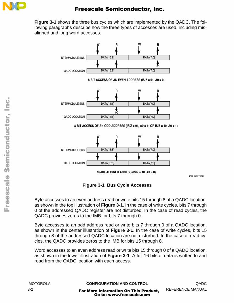
Figure 3-1 shows the three bus cycles which are implemented by the QADC. The fol-lowing paragraphs describe how the three types of accesses are used, including mis-aligned and long word accesses.
Figure 3-1 Bus Cycle Accesses
Byte accesses to an even address read or write bits 15 through 8 of a QADC location,as shown in the top illustration of Figure 3-1. In the case of write cycles, bits 7 through0 of the addressed QADC register are not disturbed. In the case of read cycles, theQADC provides zeros to the IMB for bits 7 through 0.
Byte accesses to an odd address read or write bits 7 through 0 of a QADC location,as shown in the center illustration of Figure 3-1. In the case of write cycles, bits 15through 8 of the addressed QADC location are not disturbed. In the case of read cy-cles, the QADC provides zeros to the IMB for bits 15 through 8.
Word accesses to an even address read or write bits 15 through 0 of a QADC location,as shown in the lower illustration of Figure 3-1. A full 16 bits of data is written to andread from the QADC location with each access.
QADC BUS CYC ACC
00
INTERMODULE BUS
8-BIT ACCESS OF AN EVEN ADDRESS (ISIZ = 01, A0 = 0)
DATA[15:8] DATA[7:0]
DATA[15:8] DATA[7:0]QADC LOCATION
W R W R
INTERMODULE BUS
8-BIT ACCESS OF AN ODD ADDRESS (ISIZ = 01, A0 = 1; OR ISIZ = 10, A0 = 1)
DATA[15:8] DATA[7:0]
DATA[15:8] DATA[7:0]QADC LOCATION
W R W R
INTERMODULE BUS
16-BIT ALIGNED ACCESS (ISIZ = 10, A0 = 0)
DATA[15:8] DATA[7:0]
DATA[15:8] DATA[7:0]QADC LOCATION
W R W R
00
MOTOROLA CONFIGURATION AND CONTROL QADC
3-2 REFERENCE MANUAL
For More Information On This Product, Go to: www.freescale.com

F
ree
sca
le S
em
ico
nd
uc
tor,
I
Freescale Semiconductor, Inc.n
c..
.
Word accesses to an odd address require two bus cycles; half of two different 16-bitQADC locations are accessed. The first bus cycle is treated by the QADC as an 8-bitread or write of an odd address. The second cycle is an 8-bit read or write of an evenaddress. The QADC address space is organized into 16-bit even address locations,so a 16-bit read or write of an odd address obtains or provides the lower half of oneQADC location, and the upper half of the following QADC location.
Long word (32-bit) accesses to an even address require two bus cycles to completethe access, and two full QADC locations are accessed. The first bus cycle reads orwrites the addressed 16-bit QADC location and the second cycle reads or writes thefollowing 16-bit location.
Long word accesses to an odd address require three bus cycles. Portions of three dif-ferent QADC locations are accessed. The first bus cycle is treated by the QADC as an8-bit access of an odd address, the second cycle is a 16-bit aligned access, and thethird cycle is an 8-bit access of an even address. The QADC address space is orga-nized into 16-bit even address locations, so a 32-bit read or write of an odd addressprovides the lower half of one QADC location, the full 16-bit content of the followingQADC location, and the upper half of the third QADC location.
3.3 Module Configuration
The module configuration register (QADCMCR) contains parameters which allow theQADC to interface with other MCU modules. The register defines freeze and stopmode operation, supervisor-only access protection, and the QADC software interruptarbitration priority number. The implemented fields can be read and written. Unimple-mented locations read zero and writes have no effect. They are typically written oncewhen the software initializes the QADC, and not changed afterwards.
3.3.1 Low Power Stop Mode
When the STOP bit in the QADCMCR is set, the clock signal to the A/D converter isdisabled, effectively turning off the analog circuitry. This results in a static, low powerconsumption, idle condition. The stop mode aborts any conversion sequence inprogress. Because the bias currents to the analog circuits are turned off in stop mode,the QADC requires some recovery time (TSR in APPENDIX A ELECTRICAL CHAR-ACTERISTICS) to stabilize the analog circuits after the stop enable bit is cleared.
In the stop mode, the BIU state machine and logic do not shut down, and the QADC-MCR, the interrupt register (QADCINT), and the test register (QADCTEST) are fullyaccessible and are not reset. The data direction register (DDRQA), port data register(PORTQA/PORTQB), and control register 0 (QACR0) are not reset and are read-onlyaccessible. The RAM is not reset and is not accessible. Control register 1 (QACR1),control register 2 (QACR2), and the status register (QASR) are reset and are read-onlyaccessible. In addition, the QADC clock (QCLK) and the periodic/interval timer areheld in reset during stop mode.
If the STOP bit is clear, stop mode is disabled.
QADC CONFIGURATION AND CONTROL MOTOROLA
REFERENCE MANUAL 3-3
For More Information On This Product, Go to: www.freescale.com

F
ree
sca
le S
em
ico
nd
uc
tor,
I
Freescale Semiconductor, Inc.n
c..
.
3.3.2 Freeze Mode
Freeze mode occurs when the background debug mode is enabled in the device inte-gration module and a breakpoint is encountered. This is indicated by the assertion ofthe internal FREEZE line on the IMB. The FRZ bit in the QADCMCR determineswhether or not the QADC responds to an IMB internal FREEZE signal assertion.Freeze is very useful when debugging an application.
When the FRZ bit is set, the QADC finishes any current conversion then freezes. De-pending on when the FRZ bit is asserted, there are three possible queue “freeze” sce-narios:
• When a queue is not executing, the QADC freezes immediately.• When a queue is executing, the QADC completes the current conversion and
then freezes.• If during the execution of the current conversion, the queue operating mode for
the active queue is changed, or a queue 2 abort occurs, the QADC freezes im-mediately.
When the QADC enters the freeze mode while a queue is active, the current CCW lo-cation of the queue pointer is saved.
During freeze, the analog clock is held in reset and is not clocked. Although QCLK isunaffected, the periodic/interval timer is held in reset. External trigger events that oc-cur during the freeze mode are not recorded. The BIU remains active to allow IMB ac-cess to all QADC registers and RAM. Although the QADC saves a pointer to the nextCCW in the current queue, the software can force the QADC to execute a differentCCW by writing new queue operating modes for normal operation. The QADC looksat the queue operating modes, the current queue pointer, and any pending triggerevents to decide which CCW to execute.
If the FRZ bit is clear, the internal FREEZE signal is ignored.
3.3.3 Supervisor/Unrestricted Address Space
The QADC memory map is divided into two segments: supervisor-only data space andassignable data space. Access to supervisor-only data space is permitted only whenthe software is operating in supervisor access mode. Assignable data space can beeither restricted to supervisor-only access or unrestricted to both supervisor and userdata space accesses. The SUPV bit in the QADCMCR designates the assignablespace as supervisor or unrestricted.
Attempts to read a supervisor-only data space when not in the supervisor accessmode causes a value of $0000 to be returned. Attempts to read assignable data spacein the unrestricted access mode when the space is programmed as supervisor spacecauses a value of $FFFF to be returned. Attempts to write supervisor-only or supervi-sor-assigned data space when in the unrestricted access mode has no effect.
The CPU indicates the supervisor and user space access with the function code bits(FC[2:0]) on the IMB bus.
MOTOROLA CONFIGURATION AND CONTROL QADC
3-4 REFERENCE MANUAL
For More Information On This Product, Go to: www.freescale.com

F
ree
sca
le S
em
ico
nd
uc
tor,
I
Freescale Semiconductor, Inc.n
c..
.
NOTE
Some CPUs do not support supervisor/user space selection, and arealways in the supervisor access mode. In such cases, the SUPV bithas no meaning or effect.
The supervisor-only data space segment contains the QADC global registers, whichinclude the QADCMCR, the QADCTEST, and the QADCINT. The supervisor/unre-stricted space designation for the CCW table, the result word table, and the remainingQADC registers are programmable.
3.3.4 Interrupt Arbitration Priority
Each module that can generate interrupts, including the QADC, has an IARB (interruptarbitration number) field in the QADCMCR. Each IARB field must have a different val-ue. During an interrupt acknowledge cycle, IARB permits arbitration among simulta-neous interrupts of the same priority level.
The reset value of IARB in the QADCMCR is $F. This prevents QADC interrupts frombeing discarded. Initialization software must set the IARB field to a lower value in therange $F (highest priority) to $1 (lowest priority) if lower priority interrupts are to be ar-bitrated.
Refer to SECTION 8 INTERRUPTS for more information.
3.3.5 QADC Module Configuration Register
The QADCMCR contains fields and bits that control freeze and stop modes and deter-mines the privilege level required to access most registers. It also contains the IARBfield.
STOP — Stop Enable0 = Disable stop mode.1 = Enable stop mode.
FRZ — Freeze Enable0 = Ignores the IMB internal FREEZE signal.1 = Finish any current conversion, then freeze
SUPV — Supervisor/Unrestricted Data Space0 = Only the module configuration register, test register, and interrupt register are
designated as supervisor-only data space. Access to all other locations is un-restricted.
1 = All QADC registers and tables are designated as supervisor-only data space.
QADCMCR — Module Configuration Register $####0015 14 13 12 11 10 9 8 7 6 5 4 3 2 1 0
STOP FRZ NOT USED SUPV NOT USED IARB
RESET:
0 0 1 0 0 0 0
QADC CONFIGURATION AND CONTROL MOTOROLA
REFERENCE MANUAL 3-5
For More Information On This Product, Go to: www.freescale.com
F
ree
sca
le S
em
ico
nd
uc
tor,
I
Freescale Semiconductor, Inc.n
c..
.
IARB[3:0] — Interrupt Arbitration NumberIARB determines QADC interrupt arbitration priority. An IARB field can be assigned avalue from %0001 (lowest priority) to %1111 (highest value). Refer to SECTION 8 IN-TERRUPTS for more information.
3.4 QADC Test Register
QADCTEST — QADC Test Register $####02
QADCTEST is used only during factory testing of the MCU.
3.5 General-Purpose I/O Port Operation
Each of the port pins, when used as a general-purpose input, is conditioned by a syn-chronizer with an enable feature. The synchronizer is not enabled until the QADC de-codes an IMB bus cycle which addresses the port data register to minimize the high-current effect of mid-level signals on the inputs used for analog signals. Digital inputsignals must meet the input low voltage (VIL) or input high voltage (VIH) specificationsin APPENDIX A ELECTRICAL CHARACTERISTICS. If an analog input pin does notmeet the digital input pin specifications when a digital port read operation occurs, anindeterminate state is read.
During a port data register read, the actual value of the pin is reported when its corre-sponding bit in the data direction register defines the pin to be an input (port A only).When the data direction bit specifies the pin to be an output, the content of the portdata register is read. By reading the latch which drives the output pin, software instruc-tions that read data, modify it, and write the result, like bit manipulation instructions,work correctly. When a reduced number of digital port pins are implemented on a par-ticular microcontroller version, the unused bit positions are read as a zero and writeoperations do not have any effect.
There are two special cases to consider for the digital I/O port operation. When theMUX (externally multiplexed) bit is set in QACR0, the data direction register settingsare ignored for the bits corresponding to PQA[2:0], the three multiplexed address(MA[2:0]) output pins. The MA[2:0] pins are forced to be digital outputs, regardless ofthe data direction setting, and the multiplexed address outputs are driven. The datareturned during a port data register read is the value of the multiplexed address latcheswhich drive MA[2:0], regardless of the data direction setting.
Similarly, when an external trigger queue operating mode is selected, the data direc-tion setting for the corresponding pins, PQA3 or PQA4, is ignored. The port pins areforced to be digital inputs for ETRIG1 and/or ETRIG2. The data driven during a portdata register read is the actual value of the pin, regardless of the data direction setting.
3.5.1 Port Data Register
QADC ports A and B are accessed through two 8-bit port data registers (PORTQA andPORTQB).
MOTOROLA CONFIGURATION AND CONTROL QADC
3-6 REFERENCE MANUAL
For More Information On This Product, Go to: www.freescale.com

F
ree
sca
le S
em
ico
nd
uc
tor,
I
Freescale Semiconductor, Inc.n
c..
.
Port A pins are referred to as PQA[7:0] when used as a bidirectional 8-bit input/outputport that may be used for general-purpose digital input signals or digital open drainpull-down output signals. Port A can also be used for analog inputs (AN[59:52], exter-nal trigger inputs (ETRIG[2:1]), and external multiplexer address outputs (MA[2:0]).
Port B pins are referred to as PQB[7:0] when used as an input-only 8-bit digital portthat may be used for general-purpose digital input signals. Data for PQB[7:0] is ac-cessed in the lower half of the QPDR. Port B can also be used for nonmultiplexed(AN[51:48]/AN[3:0]) and multiplexed (ANz, ANy, ANx, ANw) analog inputs.
PORTQA and PORTQB are unaffected by reset.
3.5.2 Port Data Direction Register
The port data direction register (DDRQA) is associated with the port A digital I/O pins.The bidirectional pins have somewhat higher leakage and capacitance specifications.Refer to APPENDIX A ELECTRICAL CHARACTERISTICS for more information. Anybit in this register set to one configures the corresponding pin as an output. Any bit inthis register cleared to zero configures the corresponding pin as an input. The softwareis responsible for ensuring that DDR bits are not set to one on pins used for analoginputs. When the DDR bit is set to one and the pin is selected for analog conversion,the voltage sampled is that of the output digital driver as influenced by the load.
NOTE
Caution should be exercised when mixing digital and analog inputs.This should be isolated as much as possible. Rise and fall timesshould be as large as possible to minimize AC coupling effects.
Since port B is input-only, a data direction register is not needed. Therefore, the lowerbyte of the port data direction register is not implemented. Read operations on the re-served bits return zeros, and writes have no effect.
PORTQA — Port A Data Register $####06PORTQB — Port B Data Register $####07
15 14 13 12 11 10 9 8 7 6 5 4 3 2 1 0
PQA7 PQA6 PQA5 PQA4 PQA3 PQA2 PQA1 PQA0 PQB7 PQB6 PQB5 PQB4 PQB3 PQB2 PQB1 PQB0
RESET:
U U U U U U U U U U U U U U U U
ANALOG CHANNEL:
AN59 AN58 AN57 AN56 AN55 AN54 AN53 AN52 AN51 AN50 AN49 AN48 AN3 AN2 AN1 AN0
EXTERNAL TRIGGER INPUTS:
ETRIG2 ETRIG1
MULTIPLEXED ADDRESS OUTPUTS:
MA2 MA1 MA0
MULTIPLEXED ANALOG INPUTS:
ANz ANy ANx ANw
QADC CONFIGURATION AND CONTROL MOTOROLA
REFERENCE MANUAL 3-7
For More Information On This Product, Go to: www.freescale.com

F
ree
sca
le S
em
ico
nd
uc
tor,
I
Freescale Semiconductor, Inc.n
c..
.
DDRQA — Port Data Direction Register $####0815 14 13 12 11 10 9 8 7 6 5 4 3 2 1 0
DDQA7 DDQA6 DDQA5 DDQA4 DDQA3 DDQA2 DDQA1 DDQA0 RESERVED
RESET:
0 0 0 0 0 0 0 0 0 0 0 0 0 0 0 0
MOTOROLA CONFIGURATION AND CONTROL QADC
3-8 REFERENCE MANUAL
For More Information On This Product, Go to: www.freescale.com

F
ree
sca
le S
em
ico
nd
uc
tor,
I
Freescale Semiconductor, Inc.n
c..
.
SECTION 4 EXTERNAL MULTIPLEXINGExternal multiplexer chips concentrate a number of analog signals onto a few inputsto the analog converter. This is helpful in applications that need to convert more analogsignals than the A/D converter can normally provide. External multiplexing also putsthe multiplex chip closer to the signal source. This minimizes the number of analog sig-nals that need to be shielded due to the close proximity to noisy high speed digital sig-nals at the microcontroller chip.
For example, four 8-input multiplexer chips can be put at the connector where the an-alog signals first arrive on the computer board. As a result, only four analog signalsneed to be shielded from noise as they approach the microcontroller chip, rather thanhaving to protect 32 analog signals. However, external multiplexer chips may intro-duce additional noise and errors if not properly utilized. Therefore, it is necessary tomaintain low “on” resistance (the impedance of an analog switch when active within amultiplex chip) and insert a low pass filter (R/C) on the input side of the multiplex chip.
4.1 External Multiplexing Operation
The QADC can use from one to four external multiplexer chips to expand the numberof analog signals that may be converted. Up to 32 analog channels can be convertedthrough external multiplexer selection. The externally multiplexed channels are auto-matically selected from the channel field of the conversion command word (CCW) ta-ble, the same as internally multiplexed channels. Refer to paragraph 7.7 in SECTION7 DIGITAL CONTROL for additional information on channel number assignments.
All of the automatic queue features are available for externally and internally multi-plexed channels. The software selects the external multiplexed mode by setting theMUX bit in control register 0 (QACR0).
Figure 4-1 shows the maximum configuration of four external multiplexer chips con-nected to the QADC. The external multiplexer chips select one of eight analog inputsand connect it to one analog output, which becomes an input to the QADC. The QADCprovides three multiplexed address signals — MA0, MA1, and MA2, to select one ofeight inputs. These inputs are connected to all four external multiplexer chips. The an-alog output of the four multiplex chips are each connected to four separate QADC in-puts — ANw, ANx, ANy, and ANz.
QADC EXTERNAL MULTIPLEXING MOTOROLA
REFERENCE MANUAL 4-1
For More Information On This Product, Go to: www.freescale.com
F
ree
sca
le S
em
ico
nd
uc
tor,
I
Freescale Semiconductor, Inc.n
c..
.
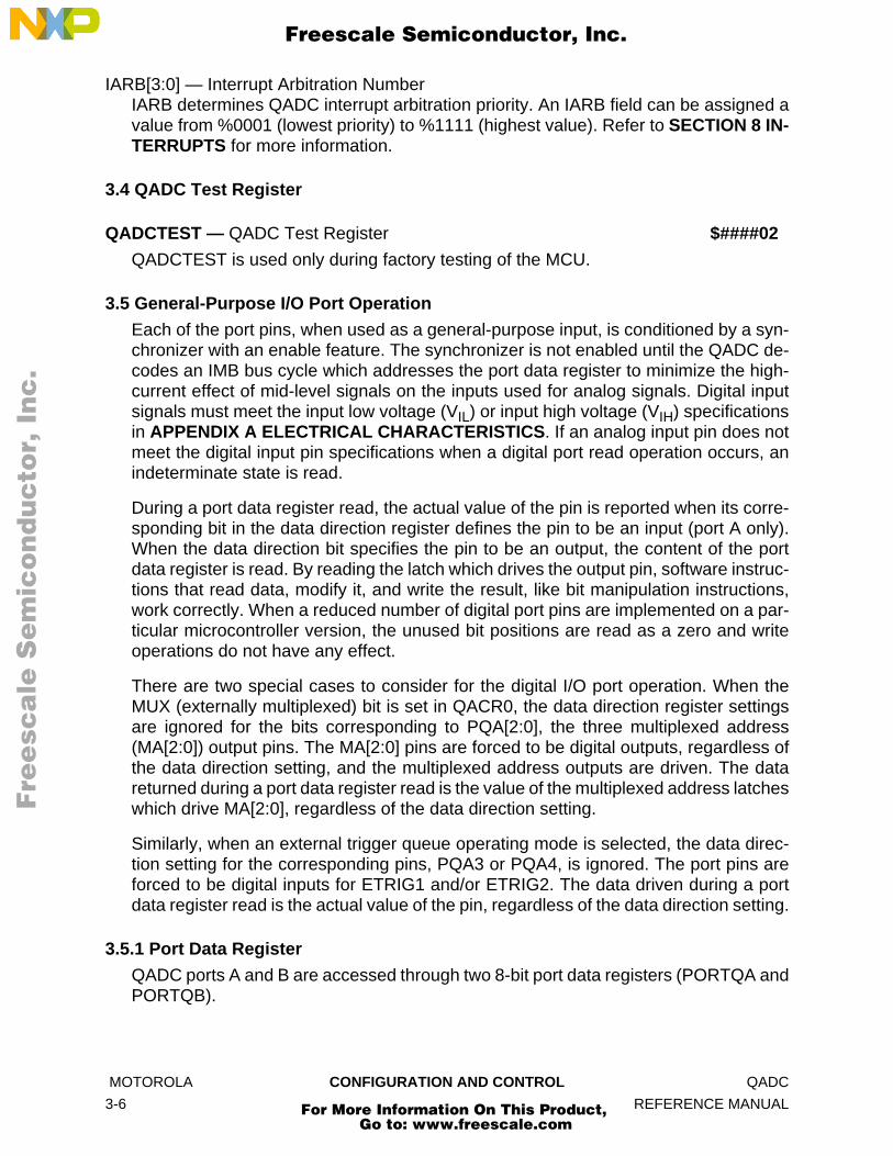
Figure 4-1 Example of External Multiplexing
When the external multiplexed mode is selected, the QADC automatically creates theMA open drain output signals from the channel number in each CCW. The QADC alsoconverts the proper input channel (ANw, ANx, ANy, and ANz) by interpreting the CCWchannel number. As a result, up to 32 externally multiplexed channels appear to theconversion queues as directly connected signals. The software simply puts the chan-nel number of externally multiplexed channels into CCWs. Refer to Table 7-9 in SEC-TION 7 DIGITAL CONTROL which shows the channel numbers for the externallymultiplexed channels that are assigned the range of channel 0 to channel 31.
Figure 4-1 shows that the three MA signals may also be analog input pins. When ex-ternal multiplexing is selected, none of the MA pins can be used for analog or digitalinputs. They become multiplexed address outputs.
QADC EXT MUX CONN
AN52/MA0/PQA0*AN53/MA1/PQA1*AN54/MA2/PQA2*
AN55/ETRIG1/PQA3*AN56/ETRIG2/PQA4*
AN57/PQA5*AN58/PQA6*AN59/PQA7*
AN0/ANW/PQB0AN1/ANX/PQB1AN2/ANY/PQB2AN3/ANZ/PQB3
AN48/PQB4AN49/PQB5AN50/PQB6AN51/PQB7 DIGITAL RESULTS
AND CONTROLANALOG
CONVERTERANALOG
MULTIPLEXER
VSSE
QADC
VDDA
VSSA
VRL
VRHMUX
AN0AN2AN4AN6AN8
AN10AN11AN12
MUX
AN1AN3AN5AN7AN9
AN11AN13AN15
MUX
AN16AN18AN20AN22AN24AN26AN28AN30
MUX
AN17AN19AN21AN23AN25AN27AN29AN31
ANALOG POWER
ANALOG REFERENCES
EXTERNAL TRIGGERS
PORT
BPO
RT A
*
* PORT A PINS INCORPORATE OPEN DRAIN PULL DOWN DRIVERS.
MOTOROLA EXTERNAL MULTIPLEXING QADC
4-2 REFERENCE MANUAL
For More Information On This Product, Go to: www.freescale.com

F
ree
sca
le S
em
ico
nd
uc
tor,
I
Freescale Semiconductor, Inc.n
c..
.
4.2 Module Version Options
The number of available analog channels varies, depending on whether or not exter-nal multiplexing is used. A maximum of 16 analog channels are supported by the in-ternal multiplexing circuitry of the converter. Table 4-1 shows the total number ofanalog input channels supported with zero to four external multiplexer chips. TheQADC uses 21 pins which allow a maximum of 41 analog channels to be converted.
NOTES:1. The above assumes that the external trigger inputs are shared with two analog input pins.2. When external multiplexing is used, three input channels become multiplexed address out-
puts, and for each external multiplexer chip, one input channel becomes a multiplexed ana-log input.
Table 4-1 Analog Input Channels
Number of Analog Input Channels AvailableDirectly Connected + External Multiplexed = Total Channels1, 2
No External Mux Chips
One External Mux Chip
Two External Mux Chips
Three External Mux Chips
Four External Mux Chips
16 12 + 8 = 20 11 + 16 = 27 10 + 24 = 34 9 + 32 = 41
QADC EXTERNAL MULTIPLEXING MOTOROLA
REFERENCE MANUAL 4-3
For More Information On This Product, Go to: www.freescale.com

F
ree
sca
le S
em
ico
nd
uc
tor,
I
Freescale Semiconductor, Inc.n
c..
.
MOTOROLA EXTERNAL MULTIPLEXING QADC
4-4 REFERENCE MANUAL
For More Information On This Product, Go to: www.freescale.com

F
ree
sca
le S
em
ico
nd
uc
tor,
I
Freescale Semiconductor, Inc.n
c..
.
SECTION 5 PIN CONNECTION CONSIDERATIONSThe QADC requires accurate, noise-free input signals for proper operation. This sec-tion discusses the design of external circuitry to maximize QADC performance.
5.1 Analog Reference Pins
No A/D converter can be more accurate than its analog reference. Any noise in thereference can result in at least that much error in a conversion. The reference for theQADC, supplied by pins VRH and VRL, should be low-pass filtered from its source toobtain a noise-free, clean signal. In many cases, simple capacitive bypassing may suf-fice. In extreme cases, inductors or ferrite beads may be necessary if noise or RF en-ergy is present. Series resistance is not advisable since there is an effective DCcurrent requirement from the reference voltage by the internal resistor string in the RCDAC array. External resistance may introduce error in this architecture under certainconditions. Any series devices in the filter network should contain a minimum amountof DC resistance.
For accurate conversion results, the analog reference voltages must be within the lim-its defined by VDDA and VSSA, as explained in the following subsection.
5.2 Analog Power Pins
The analog supply pins (VDDA and VSSA) define the limits of the analog reference volt-ages (VRH and VRL) and of the analog multiplexer inputs. Figure 5-1 is a diagram ofthe analog input circuitry.
QADC PIN CONNECTION CONSIDERATIONS MOTOROLA
REFERENCE MANUAL 5-1
For More Information On This Product, Go to: www.freescale.com
F
ree
sca
le S
em
ico
nd
uc
tor,
I
Freescale Semiconductor, Inc.n
c..
.
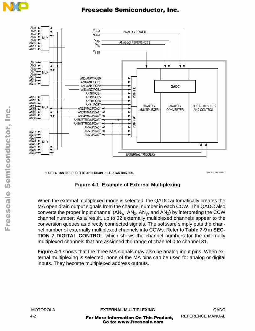
Figure 5-1 Analog Input Circuitry
Since the sample amplifier is powered by VDDA and VSSA, it can accurately transferinput signal levels up to but not exceeding VDDA and down to but not below VSSA. Ifthe input signal is outside of this range, the output from the sample amplifier is clipped.
In addition, VRH and VRL must be within the range defined by VDDA and VSSA. As longas VRH is less than or equal to VDDA and VRL is greater than or equal to VSSA and thesample amplifier has accurately transferred the input signal, resolution is ratiometricwithin the limits defined by VRL and VRH. If VRH is greater than VDDA, the sample am-plifier can never transfer a full-scale value. If VRL is less than VSSA, the sample ampli-fier can never transfer a zero value.
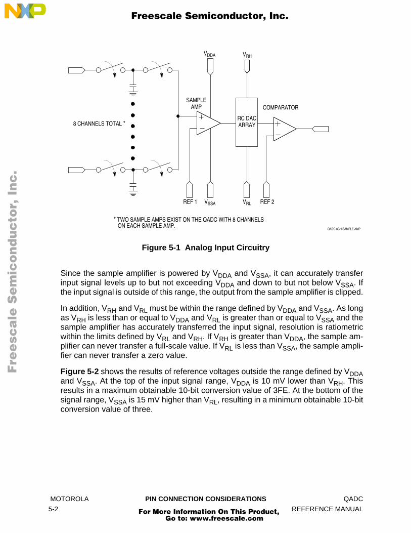
Figure 5-2 shows the results of reference voltages outside the range defined by VDDAand VSSA. At the top of the input signal range, VDDA is 10 mV lower than VRH. Thisresults in a maximum obtainable 10-bit conversion value of 3FE. At the bottom of thesignal range, VSSA is 15 mV higher than VRL, resulting in a minimum obtainable 10-bitconversion value of three.
SAMPLEAMP
8 CHANNELS TOTAL *RC DACARRAY
COMPARATOR
REF 1 VSSA VRL REF 2
VDDA VRH
QADC 8CH SAMPLE AMP
* TWO SAMPLE AMPS EXIST ON THE QADC WITH 8 CHANNELS ON EACH SAMPLE AMP.
MOTOROLA PIN CONNECTION CONSIDERATIONS QADC
5-2 REFERENCE MANUAL
For More Information On This Product, Go to: www.freescale.com
F
ree
sca
le S
em
ico
nd
uc
tor,
I
Freescale Semiconductor, Inc.n
c..
.
Figure 5-2 Errors Resulting from Clipping
5.3 Analog Supply Filtering and Grounding
Two important factors influencing performance in analog integrated circuits are supplyfiltering and grounding. Generally, digital circuits use bypass capacitors on every VDD/VSS pin pair. This applies to analog subsystems or submodules also. Equally importantas bypassing is the distribution of power and ground.
Analog supplies should be isolated from digital supplies as much as possible. This ne-cessity stems from the higher performance requirements often associated with analogcircuits. Therefore, deriving an analog supply from a local digital supply is not recom-mended. However, if for economic reasons digital and analog power are derived froma common regulator, filtering of the analog power is recommended in addition to thebypassing of the supplies already mentioned. For example, an RC low pass filter couldbe used to isolate the digital and analog supplies when generated by a common reg-ulator. If multiple high precision analog circuits are locally employed (i.e. two A/D con-verters), the analog supplies should be isolated from each other as sharing suppliesintroduces the potential for interference between analog circuits.
Grounding is the most important factor influencing analog circuit performance in mixedsignal systems (or in standalone analog systems). Close attention must be paid not tointroduce additional sources of noise into the analog circuitry. Common sources ofnoise include ground loops, inductive coupling, and combining digital and analoggrounds together inappropriately.
QADC CLIPPING
0 .020 5.100 5.110INPUT IN VOLTS (VRH = 5.120 V, VRL = 0 V)
1
2
3
4
5
6
7
8
3FA
3FB
3FC
3FD
3FE
3FF
.010 .030 5.120 5.130
10-B
IT R
ESU
LT
QADC PIN CONNECTION CONSIDERATIONS MOTOROLA
REFERENCE MANUAL 5-3
For More Information On This Product, Go to: www.freescale.com

F
ree
sca
le S
em
ico
nd
uc
tor,
I
Freescale Semiconductor, Inc.n
c..
.
The problem of how and when to combine digital and analog grounds arises from thelarge transients which the digital ground must handle. If the digital ground is not ableto handle the large transients, the current from the large transients can return toground through the analog ground. It is the excess current overflowing into the analogground which causes performance degradation by developing a differential voltagebetween the true analog ground and the microcontroller’s ground pin. The end resultis that the ground observed by the analog circuit is no longer true ground and oftenends in skewed results.
Two similar approaches designed to improve or eliminate the problems associatedwith grounding excess transient currents involve star-point ground systems. One ap-proach is to star-point the different grounds at the power supply origin, thus keepingthe ground isolated. Refer to Figure 5-3.
Figure 5-3 Star-Ground at the Point of Power Supply Origin
Another approach is to star-point the different grounds near the analog ground pin onthe microcontroller by using small traces for connecting the non-analog grounds to theanalog ground. The small traces are meant only to accommodate DC differences, notAC transients.
NOTE
This star-point scheme still requires adequate grounding for digitaland analog subsystems in addition to the star-point ground.
QADC
VRH
VRL
VSSA
VDD
A
VDD
VSS
ANALOG POWER SUPPLY
+5V+5V AGND
DIGITAL POWER SUPPLY
+5VPGND
PCB
QADC POWER SCHEM
MOTOROLA PIN CONNECTION CONSIDERATIONS QADC
5-4 REFERENCE MANUAL
For More Information On This Product, Go to: www.freescale.com

F
ree
sca
le S
em
ico
nd
uc
tor,
I
Freescale Semiconductor, Inc.n
c..
.
Other suggestions for PCB layout in which the QADC is employed include:
• Analog ground must be low impedance to all analog ground points in the circuit.• Bypass capacitors should be as close to the power pins as possible.• The analog ground should be isolated from the digital ground. This can be done
by cutting a separate ground plane for the analog ground.• Non-minimum traces should be utilized for connecting bypass capacitors and fil-
ters to their corresponding ground/power points.• Minimum distance for trace runs when possible.
5.4 Accommodating Positive/Negative Stress Conditions
Positive or negative stress refers to conditions which exceed nominally defined oper-ating limits. Examples include applying a voltage exceeding the normal limit on an in-put (for example, voltages outside of the suggested supply/reference ranges) orcausing currents into or out of the pin which exceed normal limits. QADC specific con-siderations are voltages greater than VDDA, VRH or less than VSSA applied to an analoginput which cause excessive currents into or out of the input. Refer to APPENDIX AELECTRICAL CHARACTERISTICS for more information on exact magnitudes.
Both stress conditions can potentially disrupt conversion results on neighboring inputs.Parasitic devices, associated with CMOS processes, can cause an immediate disrup-tive influence on neighboring pins. Common examples of parasitic devices are diodesto substrate and bipolar devices with the base terminal tied to substrate (VSSI/VSSAground). Under stress conditions, current introduced on an adjacent pin can cause er-rors on adjacent channels by developing a voltage drop across the adjacent externalchannel source impedances.
Figure 5-4 shows an active parasitic bipolar when an input pin is subjected to negativestress conditions. Positive stress conditions do not activate a similar parasitic device.
Figure 5-4 Input Pin Subjected to Negative Stress
The current out of the pin (IOUT) under negative stress is determined by the followingequation:
QADC PAR STRESS CONN
RSTRESS
RADJACENTADJACENT
NEGATIVE
10K
VDD
PIN UNDER
PARASITIC
IOUT
IIN
+STRESS
STRESSVOLTAGE
DEVICE
PINS
QADC PIN CONNECTION CONSIDERATIONS MOTOROLA
REFERENCE MANUAL 5-5
For More Information On This Product, Go to: www.freescale.com

F
ree
sca
le S
em
ico
nd
uc
tor,
I
Freescale Semiconductor, Inc.n
c..
.
where:
VSTRESS = Adjustable voltage source
VBE = Parasitic bipolar base/emitter voltage (refer to VNEGCLAMP in AP-PENDIX A ELECTRICAL CHARACTERISTICS)
RSTRESS = Source impedance (10K resistor in Figure 5-4 on stressedchannel)
The current into (IIN) the neighboring pin is determined by the 1/KN (Gain) of the para-sitic bipolar transistor (1/KN‹‹1).
One way to minimize the impact of stress conditions on the QADC is to apply voltagelimiting circuits such as diodes to supply and ground. However, leakage from such cir-cuits and the potential influence on the sampled voltage to be converted must be con-sidered. Refer to Figure 5-5.
Figure 5-5 Voltage Limiting Diodes in a Negative Stress Circuit
Another method for minimizing the impact of stress conditions on the QADC is to stra-tegically allocate QADC inputs so that the lower accuracy inputs are adjacent to theinputs most likely to see stress conditions.
Finally, suitable source impedances should be selected to meet design goals and min-imize the effect of stress conditions.
5.5 Analog Input Considerations
The source impedance of the analog signal to be measured and any intermediate fil-tering should be considered whether external multiplexing is used or not. Figure 5-6shows the connection of eight typical analog signal sources to one QADC analog inputpin through a separate multiplexer chip. Also, an example of an analog signal sourceconnected directly to a QADC analog input channel is displayed.
IOUT
VSTRESS VBE–
RSTRESS--------------------------------------------=
QADC NEG STRESS CONN
VDD
RkRTO DEVICEEXTERNAL VOLTAGE
VSS
MOTOROLA PIN CONNECTION CONSIDERATIONS QADC
5-6 REFERENCE MANUAL
For More Information On This Product, Go to: www.freescale.com
F
ree
sca
le S
em
ico
nd
uc
tor,
I
Freescale Semiconductor, Inc.n
c..
.
Figure 5-6 External Multiplexing Of Analog Signal Sources
~
~
~
~
~
~
~
~CIN CSAMPLE
CIN CSAMPLE
CIN = CIN + CSAMPLE
RMUXOUT
R SOURCE2
ANALOG SIGNAL SOURCEFILTERING AND INTERCONNECT
TYPICAL MUX CHIPINTERCONNECT QADC
QADC EXT MUX EX
~
C FILTER
C SOURCE
R FILTER2
C MUXIN
0.1 µF1
CMUXOUT
(MC54HC4051, MC74HC4051,MC54HC4052, MC74HC4052,
MC54HC4053, ETC.)
R SOURCE2
C FILTER
C SOURCE
R FILTER2
C MUXIN
0.1 µF1
R SOURCE2
C FILTER
C SOURCE
R FILTER2
C MUXIN
0.1 µF1
R SOURCE2
C FILTER
C SOURCE
R FILTER2
C MUXIN
0.1 µF1
R SOURCE2
C FILTER
C SOURCE
R FILTER2
C MUXIN
0.1 µF1
R SOURCE2
C FILTER
C SOURCE
R FILTER2
C MUXIN
0.1 µF1
R SOURCE2
C FILTER
C SOURCE
R FILTER2
C MUXIN
0.1 µF1
R SOURCE2
C FILTER
C SOURCE
R FILTER2
C MUXIN
0.1 µF1
C FILTER
R FILTER2
0.1 µF1
1. TYPICAL VALUE2. RFILTER TYPICALLY 10KΩ–20KΩ.
NOTES:
R SOURCE2
C SOURCE
QADC PIN CONNECTION CONSIDERATIONS MOTOROLA
REFERENCE MANUAL 5-7
For More Information On This Product, Go to: www.freescale.com
F
ree
sca
le S
em
ico
nd
uc
tor,
I
Freescale Semiconductor, Inc.n
c..
.
5.6 Analog Input Pins
Analog inputs should have low AC impedance at the pins. Low AC impedance can berealized by placing a capacitor with good high frequency characteristics at the inputpin of the part. Ideally, that capacitor should be as large as possible (within the practi-cal range of capacitors that still have good high frequency characteristics). This capac-itor has two effects:
• It helps attenuate any noise that may exist on the input. • It sources charge during the sample period when the analog signal source is a
high-impedance source.
Series resistance can be used with the capacitor on an input pin to implement a simpleRC filter. The maximum level of filtering at the input pins is application dependent andis based on the bandpass characteristics required to accurately track the dynamiccharacteristics of an input. Simple RC filtering at the pin may be limited by the sourceimpedance of the transducer or circuit supplying the analog signal to be measured. (re-fer to 5.6.2 Error Resulting from Leakage). In some cases, the size of the capacitorat the pin may be very small.
Figure 5-7 is a simplified model of an input channel. Refer to this model in the follow-ing discussion of the interaction between the external circuitry and the circuitry insidethe QADC.
Figure 5-7 Electrical Model of an A/D Input Pin
In Figure 5-7, RF and CF comprise the external filter circuit. CS is the internal samplecapacitor. Each channel has its own capacitor. CS is never precharged; it retains thevalue of the last sample. VI is an internal voltage source used to precharge the DAC
QADC SAMPLE AMP MODEL
S1 S2
AMP
RF S4S3
CDAC VICSCFVSRC
INTERNAL CIRCUIT MODELEXTERNAL CIRCUIT
= SOURCE VOLTAGE
= INTERNAL CAPACITANCE (FOR A BYPASSED CHANNEL, THIS IS THE CDAC CAPACITANCE)
VSRCRFCFCS
CDACVI
= FILTER IMPEDANCE (SOURCE IMPEDANCE INCLUDED)= FILTER CAPACITOR
= DAC CAPACITOR ARRAY= INTERNAL VOLTAGE SOURCE FOR PRECHARGE (VDDA/2)
MOTOROLA PIN CONNECTION CONSIDERATIONS QADC
5-8 REFERENCE MANUAL
For More Information On This Product, Go to: www.freescale.com
F
ree
sca
le S
em
ico
nd
uc
tor,
I
Freescale Semiconductor, Inc.n
c..
.
capacitor array (CDAC) before each sample. The value of this supply is VDDA/2, or 2.5volts for 5-volt operation.
The following paragraphs provide a simplified description of the interaction betweenthe QADC and the user's external circuitry. This circuitry is assumed to be a simple RClow-pass filter passing a signal from a source to the QADC input pin. The followingsimplifying assumptions are made:
• The source impedance is included with the series resistor of the RC filter.• The external capacitor is perfect (no leakage, no significant dielectric absorption
characteristics, etc.)• All parasitic capacitance associated with the input pin is included in the value of
the external capacitor.• Inductance is ignored.• The "on" resistance of the internal switches is zero ohms and the "off" resistance
is infinite.
5.6.1 Settling Time for the External Circuit
The values for RF and CF in the user's external circuitry determine the length of timerequired to charge CF to the source voltage level (VSRC). At time t = 0, S1 in Figure 5-7 closes. S2 is open, disconnecting the internal circuitry from the external circuitry. As-sume that the initial voltage across CF is zero. As CF charges, the voltage across it isdetermined by the following equation, where t is the total charge time:
When t = 0, the voltage across CF = 0. As t approaches infinity, VCF will equal VSRC.(This assumes no internal leakage.) With 10-bit resolution, 1/2 of a count is equal to1/2048 full-scale value. Assuming worst case (VSRC = full scale), Table 5-1 shows therequired time for CF to charge to within 1/2 of a count of the actual source voltage dur-ing 10-bit conversions. Table 5-1 is based on the RC network in Figure 5-7.
NOTE
The following times are completely independent of the A/D converterarchitecture (assuming the QADC is not affecting the charging).
Table 5-1 External Circuit Settling Time (10-Bit Conversions)
Filter Capacitor(CF)
Source Resistance (RF)100 Ω 1 kΩ 10 kΩ 100 kΩ
1 µF 760 µs 7.6 ms 76 ms 760 ms.1 µF 76 µs 760 µs 7.6 ms 76 ms.01 µF 7.6 µs 76 µs 760 µs 7.6 ms.001 µF 760 ns 7.6 µs 76 µs 760 µs100 pF 76 ns 760 ns 7.6 µs 76 µs
VCF VSRC 1 e–t– RFCF⁄
( )=
QADC PIN CONNECTION CONSIDERATIONS MOTOROLA
REFERENCE MANUAL 5-9
For More Information On This Product, Go to: www.freescale.com

F
ree
sca
le S
em
ico
nd
uc
tor,
I
Freescale Semiconductor, Inc.n
c..
.
The external circuit described in Table 5-1 is a low-pass filter. A user interested inmeasuring an AC component of the external signal must take the characteristics of thisfilter into account.
5.6.2 Error Resulting from Leakage
A series resistor limits the current to a pin, therefore input leakage acting through alarge source impedance can degrade A/D accuracy. The maximum input leakage cur-rent is specified in APPENDIX A ELECTRICAL CHARACTERISTICS. Input leakageis greatest at high operating temperatures and as a general rule decreases by one halffor each 10° C decrease in temperature.
Assuming VRH – VRL = 5.12 V, 1 count (assuming 10-bit resolution) corresponds to 5mV of input voltage. A typical input leakage of 50 nA acting through 100 kΩ of externalseries resistance results in an error of less than 1 count (5.0 mV). If the source imped-ance is 1 MΩ and a typical leakage of 50 nA is present, an error of 10 counts (50 mV)is introduced.
In addition to internal junction leakage, external leakage (e.g., if external clamping di-odes are used) and charge sharing effects with internal capacitors also contribute tothe total leakage current. Table 5-2 illustrates the effect of different levels of total leak-age on accuracy for different values of source impedance. The error is listed in termsof 10-bit counts.
CAUTION
Leakage from the part of 10 nA is obtainable only within a limited tem-perature range.
Table 5-2 Error Resulting From Input Leakage (IOFF)
SourceImpedance
Leakage Value (10-bit Conversions)10 nA 50 nA 100 nA 1000 nA
1 kΩ — — — 0.2 counts10 kΩ — 0.1 counts 0.2 counts 2 counts100 kΩ 0.2 counts 1 count 2 counts 20 counts
MOTOROLA PIN CONNECTION CONSIDERATIONS QADC
5-10 REFERENCE MANUAL
For More Information On This Product, Go to: www.freescale.com

F
ree
sca
le S
em
ico
nd
uc
tor,
I
Freescale Semiconductor, Inc.n
c..
.
SECTION 6 ANALOG SUBSYSTEMThis section describes the QADC analog subsystem, which includes the front-end an-alog multiplexer, digital to analog converter (DAC) array, the comparator, and the suc-cessive approximation register (SAR).
6.1 Analog-to-Digital Converter Operation
The analog subsystem consists of the path from the input pins through the input mul-tiplexing circuitry, into the DAC array, and through the analog comparator. The outputof the comparator feeds into the SAR and is considered the boundary between the an-alog and digital subsystems of the QADC. Figure 6-1 shows a block diagram of theQADC analog submodule.
Figure 6-1 QADC Module Block Diagram
CLOCK
PQA7
PQA0
PQB7
PQB0
CHAN. MUX
VDDA
VSSA
SAMPLE/
MUX 4: 1
10-BIT
COMPAR-
CHARGE
SUCCESSIVE
PORT PQA PORT PQB
RESULT
BUS
PERIODICSAMPLE
IMB
ADDRESS
ADDR
DATA
CLOCK
EXTERNAL
ALIGNMENT
DECODEINPUTI/O
CONTROL REGISTERSAND CONTROL LOGIC
TIMERTIMER
16: 2
TRIGGERS
ATOR
RC-DACVRH
VRL
ADDRESSDECODE
RESULT TABLE
CCW TABLE10-BIT,
10-BIT,
PUMPANDBIAS
40-WORDRAM
40-WORDRAM
DAC
HOLD
SAMPLE/HOLD PRESCALER
INTER-MODULE
BUS
INTER-FACE
APPROXIMATIONREGISTER
DUMMY
QADC DETAIL BLOCK
QADC ANALOG SUBSYSTEM MOTOROLA
REFERENCE MANUAL 6-1
For More Information On This Product, Go to: www.freescale.com

F
ree
sca
le S
em
ico
nd
uc
tor,
I
Freescale Semiconductor, Inc.n
c..
.
6.1.1 Conversion Cycle Times
Total conversion time is made up of initial sample time, transfer time, final sample time,and resolution time. Initial sample time refers to the time during which the selected in-put channel is connected to the sample capacitor at the input of the sample buffer am-plifier. During the transfer period, the sample capacitor is disconnected from themultiplexer, and the stored voltage is buffered and transferred to the RC DAC array.During the final sampling period, the sample capacitor and amplifier are bypassed,and the multiplexer input charges the RC DAC array directly. During the resolution pe-riod, the voltage in the RC DAC array is converted to a digital value and stored in theSAR.
Initial sample time is fixed at two QCLKs and the transfer time at four QCLKs. Finalsample time can be 2, 4, 8, or 16 ADC clock cycles, depending on the value of the ISTfield in the CCW. Resolution time is ten cycles.
Transfer and resolution require a minimum of 18 QCLK clocks (8.6 µs with a 2.1-MHzQCLK). If the maximum final sample time period of 16 QCLKs is selected, the totalconversion time is 15.2 µs (with a 2.1-MHz QCLK).
Figure 6-2 illustrates the timing for conversions. This diagram assumes a final sam-pling period of two QCLKs.
Figure 6-2 Conversion Timing
6.1.1.1 Amplifier Bypass Mode Conversion Timing
If the amplifier bypass mode is enabled for a conversion by setting the amplifier bypass(BYP) field in the CCW, the timing changes to that shown in Figure 6-3. Refer to para-graph 7.7 in SECTION 7 DIGITAL CONTROL for more information on the BYP field.The initial sample time and the transfer time are eliminated reducing the potential con-version time by six QCLKs. However, due to internal RC effects, a minimum final sam-
INITIAL
SAMPLETIME
TRANSFERTIME
FINAL SAMPLE
TIME RESOLUTIONTIME
SAMPLE AND TRANSFERTIME
SUCCESSIVE APPROXIMATION RESOLUTIONSEQUENCE
2 CYCLES 4 CYCLES
N CYCLES:
10 CYCLES
QCLK
(2, 4, 8, 16)
QADC CONVERSION TIM
MOTOROLA ANALOG SUBSYSTEM QADC
6-2 REFERENCE MANUAL
For More Information On This Product, Go to: www.freescale.com

F
ree
sca
le S
em
ico
nd
uc
tor,
I
Freescale Semiconductor, Inc.n
c..
.
ple time of four QCLKs must be allowed. This results in a savings of four QCLKs.When using the bypass mode, the external circuit should be of low source impedance(typically less than 10 kΩ). Also, the loading effects of the external circuitry by theQADC need to be considered, since the benefits of the sample amplifier are notpresent.
Figure 6-3 Bypass Mode Conversion Timing
6.2 Front-End Analog Multiplexer
The internal multiplexer selects one of the 16 analog input pins or one of three specialinternal reference channels for conversion. The following are the three special chan-nels:
• VRH — Reference Voltage High• VRL — Reference Voltage Low• VDDA/2 — Mid-Analog Supply Voltage
The selected input is connected to one side of the DAC capacitor array. The other sideof the DAC array is connected to the comparator input. The multiplexer also includespositive and negative stress protection circuitry, which prevents other channels fromaffecting the current conversion when voltage levels are applied to the other channels.Refer to APPENDIX A ELECTRICAL CHARACTERISTICS for specific voltage levellimits.
6.3 Digital to Analog Converter Array
The digital to analog converter (DAC) array consists of binary-weighted capacitors anda resistor-divider chain. The array serves two purposes:
• The array holds the sampled input voltage during conversion.• The resistor-capacitor array provides the mechanism for the successive approx-
imation A/D conversion.• Resolution begins with the most significant bit (MSB) and works down to the least
significant bit (LSB). The switching sequence is controlled by the digital logic.
SAMPLETIME RESOLUTION
TIME
SAMPLETIME
SUCCESSIVE APPROXIMATION RESOLUTIONSEQUENCE
N CYCLES: 10 CYCLES
QCLK
(2, 4, 8, 16)
QADC BYP CONVERSION TIM
QADC ANALOG SUBSYSTEM MOTOROLA
REFERENCE MANUAL 6-3
For More Information On This Product, Go to: www.freescale.com

F
ree
sca
le S
em
ico
nd
uc
tor,
I
Freescale Semiconductor, Inc.n
c..
.
6.4 Comparator
The comparator is used during the approximation process to sense whether the digi-tally selected arrangement of the DAC array produces a voltage level higher or lowerthan the sampled input. The comparator output feeds into the SAR which accumulatesthe A/D conversion result sequentially, starting with the MSB.
6.5 Successive Approximation Register
The input of the successive approximation register (SAR) is connected to the compar-ator output. The SAR sequentially receives the conversion value one bit at a time,starting with the MSB. After accumulating the 10 bits of the conversion result, the SARdata is transferred to the appropriate result location, where it may be read from the IMBby user software.
MOTOROLA ANALOG SUBSYSTEM QADC
6-4 REFERENCE MANUAL
For More Information On This Product, Go to: www.freescale.com

F
ree
sca
le S
em
ico
nd
uc
tor,
I
Freescale Semiconductor, Inc.n
c..
.
SECTION 7 DIGITAL CONTROLThe digital control subsystem includes the control logic to sequence the conversionactivity, channel select logic, the clock and periodic/interval timer, control and statusregisters, the conversion command word table RAM, and the result word table RAM.
The central element for control of the QADC conversions is the 40-entry conversioncommand word (CCW) table. Each CCW specifies the conversion of one input chan-nel. Depending on the application, one or two queues can be established in the CCWtable. A queue is a scan sequence of one or more input channels. By using a pausemechanism, subqueues can be created in the two queues. Each queue can be oper-ated using several different scan modes. The scan modes for queue 1 and queue 2are programmed in QACR1 and QACR2 (control registers 1 and 2). Once a queue hasbeen started by a trigger event (any of the ways to cause the QADC to begin executingthe CCWs in a queue or subqueue), the QADC performs a sequence of conversionsand places the results in the result word table.
7.1 Queue Priority
Queue 1 has priority over queue 2 execution. The following cases show the conditionsunder which queue 1 asserts its priority:
• When a queue is not active, a trigger event for queue 1 or queue 2 causes thecorresponding queue execution to begin.
• When queue 1 is active and a trigger event occurs for queue 2, queue 2 cannotbegin execution until queue 1 reaches completion or the paused state. The statusregister records the trigger event by reporting the queue 2 status as trigger pend-ing. Additional trigger events for queue 2, which occur before execution can be-gin, are recorded as trigger overruns.
• When queue 2 is active and a trigger event occurs for queue 1, the current queue2 conversion is aborted. The status register reports the queue 2 status as sus-pended. Any trigger events occurring for queue 2 while queue 2 is suspended arerecorded as trigger overruns. Once queue 1 reaches the completion or thepaused state, queue 2 begins executing again. The programming of the resumebit in QACR2 determines which CCW is executed in queue 2. Refer to 7.6.3 Con-trol Register 2 for more information.
• When simultaneous trigger events occur for queue 1 and queue 2, queue 1 be-gins execution and the queue 2 status is changed to trigger pending.
• Subqueues that are paused.
The pause feature can be used to divide queue 1 and/or queue 2 into multiple sub-queues. A subqueue is defined by setting the pause bit in the last CCW of the sub-queue.
QADC DIGITAL CONTROL MOTOROLA
REFERENCE MANUAL 7-1
For More Information On This Product, Go to: www.freescale.com
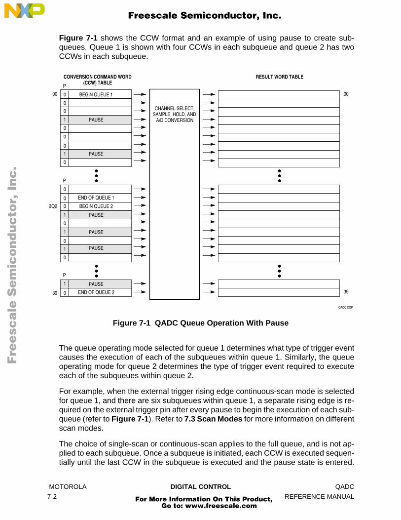
F
ree
sca
le S
em
ico
nd
uc
tor,
I
Freescale Semiconductor, Inc.n
c..
.
Figure 7-1 shows the CCW format and an example of using pause to create sub-queues. Queue 1 is shown with four CCWs in each subqueue and queue 2 has twoCCWs in each subqueue.
Figure 7-1 QADC Queue Operation With Pause
The queue operating mode selected for queue 1 determines what type of trigger eventcauses the execution of each of the subqueues within queue 1. Similarly, the queueoperating mode for queue 2 determines the type of trigger event required to executeeach of the subqueues within queue 2.
For example, when the external trigger rising edge continuous-scan mode is selectedfor queue 1, and there are six subqueues within queue 1, a separate rising edge is re-quired on the external trigger pin after every pause to begin the execution of each sub-queue (refer to Figure 7-1). Refer to 7.3 Scan Modes for more information on differentscan modes.
The choice of single-scan or continuous-scan applies to the full queue, and is not ap-plied to each subqueue. Once a subqueue is initiated, each CCW is executed sequen-tially until the last CCW in the subqueue is executed and the pause state is entered.
QADC CQP
00 BEGIN QUEUE 1
BQ2
39
END OF QUEUE 1
BEGIN QUEUE 2
END OF QUEUE 2
00
39
CHANNEL SELECT,SAMPLE, HOLD, AND
A/D CONVERSION
CONVERSION COMMAND WORD(CCW) TABLE
RESULT WORD TABLE
0
P
0
0
1
0
0
0
1
0
0
0
0
1
0
1
0
1
0
P
1
P
0
PAUSE
PAUSE
PAUSE
PAUSE
PAUSE
PAUSE
MOTOROLA DIGITAL CONTROL QADC
7-2 REFERENCE MANUAL
For More Information On This Product, Go to: www.freescale.com
F
ree
sca
le S
em
ico
nd
uc
tor,
I
Freescale Semiconductor, Inc.n
c..
.
Execution can only continue with the next CCW, which is the beginning of the nextsubqueue. A subqueue cannot be executed a second time before the overall queueexecution has been completed. Refer to 7.6.3 Control Register 2 for more informa-tion.
Trigger events which occur during the execution of a subqueue are ignored, exceptthat the trigger overrun flag is set. When a continuous-scan mode is selected, a triggerevent occurring after the completion of the last subqueue (after the queue completionflag is set), causes the execution to continue with the first subqueue, starting with thefirst CCW in the queue.
When the QADC encounters a CCW with the pause bit set, the queue enters thepaused state after completing the conversion specified in the CCW with the pause bit.The pause flag is set and a pause software interrupt may optionally be issued. The sta-tus of the queue is shown to be paused, indicating completion of a subqueue. TheQADC then waits for another trigger event to again begin execution of the next sub-queue.
7.2 Boundary Conditions
The following are queue operation boundary conditions:
• The first CCW in a queue contains channel 63, the end-of-queue (EOQ) code.The queue becomes active and the first CCW is read. The end-of-queue is rec-ognized, the completion flag is set, and the queue becomes idle. A conversion isnot performed.
• BQ2 (beginning of queue 2) is set beyond the end of the CCW table (40–63) anda trigger event occurs on queue 2. Refer to 7.6.3 Control Register 2 for informa-tion on BQ2. The end-of-queue condition is recognized immediately, the comple-tion flag is set, and the queue becomes idle. A conversion is not performed.
• BQ2 is set to CCW0 and a trigger event occurs on queue 1. After reading CCW0,the end-of-queue condition is recognized, the completion flag is set, and thequeue becomes idle. A conversion is not performed.
NOTE
Multiple end-of-queue conditions may be recognized simultaneously,although there is no change in the QADC behavior. For example, ifBQ2 is set to CCW0, CCW0 contains the EOQ code, and a triggerevent occurs on queue 1, the QADC reads CCW0 and detects bothend-of-queue conditions. The completion flag is set and queue 1 be-comes idle.
Boundary conditions also exist for combinations of pause and end-of-queue. One caseis when a pause bit is in one CCW and an end-of-queue condition is in the next CCW.The conversion specified by the CCW with the pause bit set completes normally. Thepause flag is set. However, since the end-of-queue condition is recognized, the com-pletion flag is also set and the queue status becomes idle, not paused. Examples ofthis situation include:
QADC DIGITAL CONTROL MOTOROLA
REFERENCE MANUAL 7-3
For More Information On This Product, Go to: www.freescale.com
F
ree
sca
le S
em
ico
nd
uc
tor,
I
Freescale Semiconductor, Inc.n
c..
.
• The pause bit is set in CCW5 and the channel 63 (EOQ) code is in CCW6.• The pause is in CCW39.• During queue 1 operation, the pause bit is set in CCW20 and BQ2 points to
CCW21.
Another pause and end-of-queue boundary condition occurs when the pause and anend-of-queue condition occur in the same CCW. Both the pause and end-of-queueconditions are recognized simultaneously. The end-of-queue condition has prece-dence so a conversion is not performed for the CCW and the pause flag is not set. TheQADC sets the completion flag and the queue status becomes idle. Examples of thissituation are:
• The pause bit is set in CCW10 and EOQ is programmed into CCW10.• During queue 1 operation, the pause bit set in CCW32, which is also BQ2.
7.3 Scan Modes
The QADC queuing mechanism allows the application to utilize different requirementsfor automatically scanning input channels.
In single-scan mode, a single pass through a sequence of conversions defined by aqueue is performed.
In continuous-scan mode, multiple passes through a sequence of conversions definedby a queue is executed. The following paragraphs describe single-scan and continu-ous-scan operations.
7.3.1 Disabled Mode and Reserved Mode
When the disabled mode or a reserved mode is selected, the queue is not active. Trig-ger events cannot initiate queue execution. When both queue 1 and queue 2 are dis-abled, wait states are not encountered for IMB accesses of the RAM. When bothqueues are disabled, it is safe to change the prescaler values.
7.3.2 Single-Scan Modes
When the application software wants to execute a single pass through a sequence ofconversions defined by a queue, a single-scan queue operating mode is selected. Byprogramming the MQ1 field in QACR1, the following modes can be selected for queue1:
• Software initiated single-scan mode• External trigger rising edge single-scan mode• External trigger falling edge single-scan mode
In addition to the above modes, queue 2 can also be programmed for the interval timersingle-scan mode, using the periodic/interval timer. The queue operating mode forqueue 2 is selected by the MQ2 field in QACR2.
In all single-scan queue operating modes, the software must also enable the queue tobegin execution by writing the single-scan enable bit to a one in the queue’s controlregister. The single-scan enable bits, SSE1 and SSE2, are provided for queue 1 andqueue 2 respectively.
MOTOROLA DIGITAL CONTROL QADC
7-4 REFERENCE MANUAL
For More Information On This Product, Go to: www.freescale.com

F
ree
sca
le S
em
ico
nd
uc
tor,
I
Freescale Semiconductor, Inc.n
c..
.
Until the single-scan enable bit is set, any trigger events for that queue are ignored.The single-scan enable bit may be set to a one during the write cycle, which selectsthe single-scan queue operating mode. The single-scan enable bit can be written as aone or a zero, but is always read as a zero. The completion flag, completion interrupt,or queue status are used to determine when the queue has completed.
After the single-scan enable bit is set, a trigger event causes the QADC to begin exe-cution with the first CCW in the queue. The single-scan enable bit remains set until thequeue is completed. After the queue reaches completion, the QADC resets the single-scan enable bit to zero. If the single-scan enable bit is written to a one or a zero by thesoftware before the queue scan is complete, the queue is not affected. However, if thesoftware changes the queue operating mode, the new queue operating mode and thevalue of the single-scan enable bit are recognized immediately. The current conver-sion is aborted and the new queue operating mode takes effect.
In the software initiated single-scan mode, the writing of a one to the single-scan en-able bit causes the QADC to internally generate a trigger event and the queue execu-tion begins immediately. In the other single-scan queue operating modes, once thesingle-scan enable bit is written, the selected trigger event must occur before thequeue can start. A trigger overrun is recorded if a trigger event occurs during queueexecution in the external trigger single-scan mode and the interval timer single-scanmode.
When a pause bit is encountered during the queue scan in a single-scan mode, anoth-er trigger event is required for queue execution to continue. Software involvement isnot needed to enable queue execution to continue from the paused state. The single-scan enable bit allows the entire queue to be scanned once.
In the software initiated single-scan mode, the trigger event is generated internally assoon as the conversion is complete for the CCW with the pause bit set. The pause istwo QCLKs. In the external trigger single-scan mode, the queue remains paused untilanother trigger edge is received on the external trigger pin.
In the interval timer single-scan mode, the next expiration of the timer is the triggerevent for the queue. After the queue execution is complete, the queue status is shownas idle. The software can restart the queue by setting the single-scan enable bit to aone. Queue execution begins with the first CCW in the queue.
7.3.2.1 Software Initiated Single-Scan Mode
Software can initiate the execution of a scan sequence for queue 1 or 2 by selectingthe software initiated single-scan mode, and writing the single-scan enable bit inQACR1 or QACR2. A trigger event is generated internally and the QADC immediatelybegins execution of the first CCW in the queue. If a pause is encountered, queue ex-ecution ceases momentarily while another trigger event is generated internally, andthen execution continues.
The QADC automatically performs the conversions in the queue until an end-of-queuecondition is encountered. The queue remains idle until the software again sets the sin-gle-scan enable bit. While the time to internally generate and act on a trigger event is
QADC DIGITAL CONTROL MOTOROLA
REFERENCE MANUAL 7-5
For More Information On This Product, Go to: www.freescale.com

F
ree
sca
le S
em
ico
nd
uc
tor,
I
Freescale Semiconductor, Inc.n
c..
.
very short, software can momentarily read the status conditions, indicating that thequeue is paused. The trigger overrun flag is never set while in the software initiatedsingle-scan mode.
The software initiated single-scan mode is useful in the following applications:
• Allows software complete control of the queue execution.• Allows the software to easily alternate between several queue sequences.
7.3.2.2 External Trigger Single-Scan Mode
The external trigger single-scan mode is a variation of the external trigger continuous-scan mode, and is also available with both queue 1 and queue 2. The software pro-grams the polarity of the external trigger edge that is to be detected, either a rising ora falling edge. The software must enable the scan to occur by setting the single-scanenable bit for the queue.
The first external trigger edge causes the queue to be executed one time. Each CCWis read and the indicated conversions are performed until an end-of-queue conditionis encountered. After the queue is completed, the QADC clears the single-scan enablebit. Software may set the single-scan enable bit again to allow another scan of thequeue to be initiated by the next external trigger edge.
The external trigger single-scan mode is useful when the input trigger rate can exceedthe queue execution rate. Analog samples can be taken in sync with an external event,even though the software is not interested in data taken from every edge. The softwarecan start the external trigger single-scan mode and get one set of data, and at a latertime, start the queue again for the next set of samples.
The external trigger single-scan mode is also useful when the software needs tochange the polarity of the external trigger so that both the rising and falling edgescause queue execution.
7.3.2.3 Interval Timer Single-Scan Mode
Queue 2 can also use the periodic/interval timer in a single-scan queue operatingmode. The timer interval can range from 128 to 128K QCLK cycles in binary multiples.When the interval timer single-scan mode is selected and the software sets the single-scan enable bit in QACR2, the timer begins counting. When the time interval expires,an internal trigger event is created to start the queue. The timer is reloaded and beginscounting again. Meanwhile, the QADC begins execution with the first CCW in queue 2.
The QADC automatically performs the conversions in the queue until a pause or anend-of-queue condition is encountered. When a pause occurs, queue execution stopsuntil the timer interval expires again, and queue execution continues. When the queueexecution reaches an end of queue situation, the timer is held in reset and the single-scan enable bit is cleared. Software may set the single-scan enable bit again, allowinganother scan of the queue to be initiated by the interval timer.
MOTOROLA DIGITAL CONTROL QADC
7-6 REFERENCE MANUAL
For More Information On This Product, Go to: www.freescale.com

F
ree
sca
le S
em
ico
nd
uc
tor,
I
Freescale Semiconductor, Inc.n
c..
.
The interval timer generates a trigger event whenever the time interval elapses. Thetrigger event may cause the queue execution to continue following a pause, or may beconsidered a trigger overrun. Once the queue execution is completed, the single-scanenable bit must be set again to enable the timer to count again.
The interval timer single-scan mode can be used in applications which need coherentresults, for example:
• When it is necessary that all samples are guaranteed to be taken during the samescan of the analog pins.
• When the interrupt rate in the periodic timer continuous-scan mode would be toohigh.
• In sensitive battery applications, where the single-scan mode uses less powerthan the software initiated continuous-scan mode.
7.3.3 Continuous-Scan Modes
When the application software wants to execute multiple passes through a sequenceof conversions defined by a queue, a continuous-scan queue operating mode is se-lected. By programming the MQ1 field in QACR1, the following software initiatedmodes can be selected for queue 1:
• Software initiated continuous-scan mode• External trigger rising edge continuous-scan mode• External trigger falling edge continuous-scan mode
In addition to the above modes, queue 2 can also be programmed for the periodic tim-er continuous-scan mode, where a scan is initiated at a selectable time interval usingthe on-chip periodic/interval timer. The queue operating mode for queue 2 is selectedby the MQ2 field in QACR2.
When a queue is programmed for a continuous-scan mode, the single-scan enable bitin the queue control register does not have any meaning or effect. As soon as thequeue operating mode is programmed, the selected trigger event can initiate queueexecution.
In the case of the software initiated continuous-scan mode, the trigger event is gener-ated internally and queue execution begins immediately. In the other single-scanqueue operating modes, the selected trigger event must occur before the queue canstart. A trigger overrun is recorded if a trigger event occurs during queue execution inthe external trigger continuous-scan mode and the periodic timer continuous-scanmode. When a pause bit is encountered during the scan, another trigger event is re-quired for queue execution to continue. Software involvement is not needed to enablequeue execution to continue from the paused state.
In the software initiated continuous-scan mode, the trigger event is generated internal-ly as soon as the conversion is complete for the CCW with the pause bit set. The pauseis two QCLKs. In the external trigger continuous-scan mode, the queue remainspaused until another trigger edge is received on the external trigger pin. In the periodictimer continuous-scan mode, the next expiration of the timer is the trigger event for thequeue.
QADC DIGITAL CONTROL MOTOROLA
REFERENCE MANUAL 7-7
For More Information On This Product, Go to: www.freescale.com

F
ree
sca
le S
em
ico
nd
uc
tor,
I
Freescale Semiconductor, Inc.n
c..
.
After the queue execution is complete, the queue status is shown as idle. Since thecontinuous-scan queue operating modes allow the entire queue to be scanned multi-ple times, software involvement is not needed to enable queue execution to continuefrom the idle state. The next trigger event causes queue execution to begin again,starting with the first CCW in the queue.
NOTE
It may not be possible to guarantee coherent samples since the rela-tionship between any conversion in time and any other conversionmay be variable (due to programmable trigger events, queue priori-ties, and so on).
7.3.3.1 Software Initiated Continuous-Scan Mode
When the software initiated continuous-scan mode is programmed, the trigger eventis generated automatically by the QADC. Queue execution begins immediately. If apause is encountered, queue execution ceases for two QCLKs, while another triggerevent is generated internally, and then execution continues. When the end-of-queueis reached, another internal trigger event is generated, and queue execution beginsagain from the beginning of the queue.
While the time to internally generate and act on a trigger event is very short, softwarecan momentarily read the status conditions, indicating that the queue is paused or idle.The trigger overrun flag is never set while in the software initiated continuous-scanmode.
The software initiated continuous-scan mode keeps the result registers updated morefrequently than any of the other queue operating modes. The software can alwaysread the result table to get the latest converted value for each channel. The channelsscanned are kept up to date by the QADC without software involvement. Software canread a result value at any time.
NOTE
It may not be possible to guarantee coherent samples since the rela-tionship between any conversion in time and any other conversionmay be variable (due to programmable trigger events, queue priori-ties, and so on).
The software initiated continuous-scan mode may be chosen for either queue, but isnormally used only with queue 2. When the software initiated continuous-scan modeis chosen for queue 1, that queue operates continuously and queue 2, being lower inpriority, never gets executed. The short interval of time between a queue 1 pause andthe internally generated trigger event, or between a queue 1 completion and the sub-sequent trigger event is not sufficient to allow queue 2 execution to begin.
The software initiated continuous-scan mode is a useful choice with queue 2 for con-verting channels that do not need to be synchronized to anything, or for the slow-to-change analog channels. Interrupts are normally not used with the software initiatedcontinuous-scan mode. Rather, the software reads the latest conversion result from
MOTOROLA DIGITAL CONTROL QADC
7-8 REFERENCE MANUAL
For More Information On This Product, Go to: www.freescale.com

F
ree
sca
le S
em
ico
nd
uc
tor,
I
Freescale Semiconductor, Inc.n
c..
.
the result table at any time. Once initiated, software action is not needed to sustainconversions of channel.
7.3.3.2 External Trigger Continuous-Scan Mode
The QADC provides external trigger pins for both queues. When the external triggersoftware initiated continuous-scan mode is selected, a transition on the associated ex-ternal trigger pin initiates queue execution. The polarity of the external trigger signal isprogrammable, so that the software can choose to begin queue execution on the risingor falling edge. Each CCW is read and the indicated conversions are performed untilan end-of-queue condition is encountered. When the next external trigger edge is de-tected, the queue execution begins again automatically. Software initialization is notneeded between trigger events.
Some applications need to synchronize the sampling of analog channels to externalevents. There are cases when it is not possible to use software initiation of the queuescan sequence, since interrupt response times vary.
7.3.3.3 Periodic Timer Continuous-Scan Mode
The QADC includes a dedicated periodic/interval timer for initiating a scan sequencefor queue 2 only. Software selects a programmable timer interval ranging from 128 to128K times the QCLK period in binary multiples. The QCLK period is prescaled downfrom the intermodule bus (IMB) MCU clock.
When the periodic timer continuous-scan mode is selected, the timer begins counting.After the programmed interval elapses, the timer generated trigger event starts thequeue. The timer is then reloaded and begins counting again. Meanwhile, the QADCautomatically performs the conversions in the queue until an end-of-queue conditionor a pause is encountered. When a pause occurs, the QADC waits for the periodic in-terval to expire again, then continues with the queue. After end-of-queue has been de-tected, the next trigger event causes queue execution to begin again with the firstCCW in queue 2.
The periodic timer generates a trigger event whenever the time interval elapses. Thetrigger event may cause the queue execution to continue following a pause or queuecompletion, or may be considered a trigger overrun. As with all continuous-scan queueoperating modes, software action is not needed between trigger events.
Software enables the completion interrupt when using the periodic timer continuous-scan mode. When the interrupt occurs, the software knows that the periodically col-lected analog results have just been taken. The software can use the periodic interruptto obtain non-analog inputs as well, such as contact closures, as part of a periodic lookat all inputs.
7.4 QADC Clock (QCLK) Generation
Figure 7-2 is a block diagram of the clock subsystem. The QCLK provides the timingfor the A/D converter state machine which controls the timing of the conversion. TheQCLK is also the input to a 17-stage binary divider which implements the periodic/in-
QADC DIGITAL CONTROL MOTOROLA
REFERENCE MANUAL 7-9
For More Information On This Product, Go to: www.freescale.com

F
ree
sca
le S
em
ico
nd
uc
tor,
I
Freescale Semiconductor, Inc.n
c..
.
terval timer. To retain the specified analog conversion accuracy, the QCLK frequency(FQCLK) must be within the tolerance specified in APPENDIX A ELECTRICAL CHAR-ACTERISTICS.
Before using the QADC, the software must initialize the prescaler with values that putthe QCLK within the specified range. Though most software applications initialize theprescaler once and do not change it, write operations to the prescaler fields are per-mitted.
CAUTION
A change in the prescaler value while a conversion is in progress islikely to corrupt the result from any conversion in progress. There-fore, any prescaler write operation should be done only when bothqueues are in the disabled modes.
Figure 7-2 QADC Clock Subsystem Functions
QADC CLOCK BLOCK
PRESCALER RATE SELECTION(FROM CONTROL REGISTER 0):
BINARY COUNTER
PERIODIC/INTERVALTIMER SELECT
215214213212211210292827 216 217
ONE'S COMPLEMENTCOMPARE
CLOCKGENERATE
5-BIT DOWN COUNTER
ZERODETECT
RESET QCLK
LOAD PSH
SET QCLK
QCLK
QADC CLOCK( ÷2 TO ÷40 )
LOW TIME CYCLES (PSL)
ADD HALF CYCLE TO HIGH (PSA)
HIGH TIME CYCLES (PSH)
INPUT SAMPLE TIME (FROM CCW)
QUEUE 2 MODE RATE SELECTION(FROM CONTROL REGISTER 2):
SAR CONTROL
SAR[9:0]
PERIODIC/INTERVALTRIGGER EVENT
5 3
3
3
1
5
4
SYSTEM CLOCK (FSYS)
A/D CONVERTERSTATE MACHINE
MOTOROLA DIGITAL CONTROL QADC
7-10 REFERENCE MANUAL
For More Information On This Product, Go to: www.freescale.com

F
ree
sca
le S
em
ico
nd
uc
tor,
I
Freescale Semiconductor, Inc.n
c..
.
To accommodate wide variations of the main MCU clock frequency (IMB system clock– FSYS), QCLK is generated by a programmable prescaler which divides the MCU sys-tem clock to a frequency within the specified QCLK tolerance range. To allow the A/Dconversion time to be maximized across the spectrum of system clock frequencies,the QADC prescaler permits the frequency of QCLK to be software selectable. It alsoallows the duty cycle of the QCLK waveform to be programmable.
The software establishes the basic high phase of the QCLK waveform with the PSH(prescaler clock high time) field in QACR0, and selects the basic low phase of QCLKwith the PSL (prescaler clock low time) field. The duty cycle of the QCLK can be furthermodified with the PSA (prescaler add a clock tic) bit in QACR0. The combination of thePSH and PSL parameters establishes the frequency of the QCLK.
Figure 7-2 shows that the prescaler is essentially a variable pulse width signal gener-ator. A 5-bit down counter, clocked at the system clock rate, is used to create both thehigh phase and the low phase of the QCLK signal. At the beginning of the high phase,the 5-bit counter is loaded with the 5-bit PSH value. When the zero detector finds thatthe high phase is finished, the QCLK is reset. A 3-bit comparator looks for a one’s com-plement match with the 3-bit PSL value, which is the end of the low phase of the QCLK.The PSA bit allows the QCLK high-to-low transition to be delayed by a half cycle of theinput clock.
The following sequence summarizes the process of determining what values are to beput into the prescaler fields in QACR0:
1. Choose the system clock frequency (FSYS).2. Choose first-try values for PSH, PSL, and PSA, then skip to step 4.3. Choose different values for PSH, PSL, and PSA.4. If High QCLK Time is less than TPSH (QADC Clock Duty Cycle – Minimum High
Phase Time), return to step 3. Refer to APPENDIX A ELECTRICAL CHARAC-TERISTICS for more information on TPSH.
NOTEHigh QCLK Time (in ns) = 1000 (PSH + 1 + 0.5 PSA) ÷ FSYS (in MHz)
5. If Low QCLK Time is less than TPSL (QADC Clock Duty Cycle – Minimum LowPhase Time), return to step 3. Refer to APPENDIX A ELECTRICAL CHARAC-TERISTICS for more information on TPSL.
NOTELow QCLK Time (in ns) = 1000 (PSL + 1 – 0.5 PSA) ÷ FSYS (in MHz)
6. Calculate the QCLK frequency (FQCLK).
NOTEFQCLK (in MHz) = 1000 ÷ (High QCLK Time + Low QCLK Time)
7. Choose the number of input sample cycles for a typical input channel.8. If the calculated conversion times are not sufficient, return to step 3.
QADC DIGITAL CONTROL MOTOROLA
REFERENCE MANUAL 7-11
For More Information On This Product, Go to: www.freescale.com

F
ree
sca
le S
em
ico
nd
uc
tor,
I
Freescale Semiconductor, Inc.n
c..
.
9. Code the selected PSH, PSL, and PSA values into the prescaler fields ofQACR0.
Figure 7-3 and Table 7-1 show examples of QCLK programmability. The examplesinclude conversion times based on the following assumptions:
• System clock (FSYS) = 20.97 MHz.• Input sample time is as fast as possible (IST = 0, 2 QCLK cycles).
Figure 7-3 and Table 7-1 also show the conversion time calculated for a single con-version in a queue. For other MCU system clock frequencies and other input sampletimes, the same calculations can be made.
Figure 7-3 QADC Clock Programmability Examples
The MCU system clock frequency is the basis of the QADC timing. The QADC requiresthat the system clock frequency be at least twice the QCLK frequency. Refer to AP-PENDIX A ELECTRICAL CHARACTERISTICS for information on the minimum andmaximum allowable QCLK frequencies.
The QCLK frequency is established by the combination of the PSH and PSL parame-ters in QACR0. The 5-bit PSH field selects the number of system clock cycles in thehigh phase of the QCLK wave. The 3-bit PSL field selects the number of system clockcycles in the low phase of the QCLK wave.
Example 1 in Figure 7-3 shows that when PSH = 3, the QCLK remains high for fourcycles of the system clock. It also shows that when PSL = 3, the QCLK remains lowfor four system clock cycles. In example 1, the equation for QCLK high cycles is thePSH value plus one, and the equation for the QCLK low cycles is the PSL value plusone.
Table 7-1 QADC Clock Programmability
Control Register 0 Information FSYS = 20.97Input Sample Time (IST) = %00
Example Number
PSH PSA PSL QCLK(MHz)
Conversion Time(µs)
1 7 0 7 1.0 18.02 7 1 7 1.0 18.0
QCLK EXAMPLES
FSYS
EX1
EX2
SYSTEM CLOCK
QADC QCLK EX16 CYCLES
MOTOROLA DIGITAL CONTROL QADC
7-12 REFERENCE MANUAL
For More Information On This Product, Go to: www.freescale.com

F
ree
sca
le S
em
ico
nd
uc
tor,
I
Freescale Semiconductor, Inc.n
c..
.
Refer to APPENDIX A ELECTRICAL CHARACTERISTICS for information on mini-mum QCLK high time (TPSH) and the minimum QCLK low time (TPSL).
In order to be able to tune the QCLK as close as possible to the fastest conversiontime for any given system clock frequency, the QADC permits one more programma-ble control of the QCLK high and low time. The PSA parameter in QACR0 allows theQCLK high phase to be stretched for a half cycle of the system clock, and correspond-ingly, the QCLK low phase is shortened by a half cycle of the system clock.
Example 2 in Figure 7-3 is the same as Example 1, except that the PSA bit is set. TheQCLK high phase has 4.5 system clock cycles; the QCLK low phase has 3.5 systemclock cycles.
The following are equations for calculating the QCLK high and low phases:
• High QCLK Time = 1000 (PSH + 1 + 0.5 PSA) ÷ FSYS (in ns)• Low QCLK Time = 1000 (PSL + 1 – 0.5 PSA) ÷ FSYS (in ns)• FQCLK = 1000 ÷ (High QCLK Time + Low QCLK Time) (in MHz)
Where:
• PSH = 0 to 31, the prescaler QCLK high cycles in QACR0• PSL = 0 to 7, the prescaler QCLK low cycles in QACR0• PSA = 0 to 1, the prescaler QCLK add half cycle in QACR0• FSYS = System clock frequency in MHz• FQCLK = QCLK frequency in MHz
7.5 Periodic/Interval Timer
The on-chip periodic/interval timer is enabled to generate trigger events at a program-mable interval, initiating execution of queue 2. The periodic/interval timer stays resetunder the following conditions:
• Queue 2 is programmed to any queue operating mode which does not use theperiodic/interval timer
• Interval timer single-scan mode is selected, but the single-scan enable bit is setto zero
• IMB system reset or the master reset is asserted• Stop mode is selected• Freeze mode is selected
Two other conditions which cause a pulsed reset of the timer are:
• Roll over of the timer counter• A queue operating mode change from one periodic/interval timer mode to another
periodic/interval timer mode
During the stop mode, the periodic/interval timer is held in reset. Since stop modecauses QACR2 to be initialized to zero, a valid periodic or interval timer mode must bewritten to QACR2 after stop mode is exited to release the timer from reset.
When the IMB internal FREEZE line is asserted and a periodic or interval timer mode
QADC DIGITAL CONTROL MOTOROLA
REFERENCE MANUAL 7-13
For More Information On This Product, Go to: www.freescale.com

F
ree
sca
le S
em
ico
nd
uc
tor,
I
Freescale Semiconductor, Inc.n
c..
.
is selected, the timer counter is reset after the current conversion completes. Whenthe periodic or interval timer mode has been enabled (the timer is counting), but a trig-ger event has not been issued, the freeze mode takes effect immediately, and the tim-er is held in reset. When the internal FREEZE line is negated, the timer counter startscounting from the beginning. Refer to paragraph 3.3.2 in SECTION 3 CONFIGURA-TION AND CONTROL for more information.
7.6 Control and Status Registers
The following paragraphs describe the control and status registers. The QADC hasthree control registers and one status register.
7.6.1 Control Register 0
Control register 0 establishes the QCLK with prescaler parameter fields and defineswhether external multiplexing is enabled. All of the implemented control register fieldscan be read or written, reserved locations read zero and writes have no effect. Theyare typically written once when the software initializes the QADC, and not changed af-terwards.
MUX — Externally Multiplexed ModeThe MUX bit allows the software to select the externally multiplexed mode, which af-fects the interpretation of the channel numbers and forces the MA0, MA1 and MA2pins to be outputs.
0 = Internally multiplexed, 16 possible channels.1 = Externally multiplexed, 44 possible channels.
PSH[8:4] — Prescaler Clock High TimeThe PSH field selects the QCLK high time in the prescaler. Refer to APPENDIX AELECTRICAL CHARACTERISTICS for information on QADC operating clock fre-quency (FQCLK) values. To keep the QCLK within the specified range, the PSH field se-lects the high time of the QCLK, which can range from 1 to 32 system clock cycles.The minimum high time for the QCLK is specified as TPSH.
Table 7-2 displays the bits in PSH field which enable a range of QCLK high times.
QACR0 — Control Register 0 $####0A15 14 13 12 11 10 9 8 7 6 5 4 3 2 1 0
MUX RESERVED PSH PSA PSL
RESET:
0 0 0 0 1 1 0 0 1 1
MOTOROLA DIGITAL CONTROL QADC
7-14 REFERENCE MANUAL
For More Information On This Product, Go to: www.freescale.com

F
ree
sca
le S
em
ico
nd
uc
tor,
I
Freescale Semiconductor, Inc.n
c..
.
PSA — Prescaler Add a Clock TicPSA adds a system clock tic to the QCLK high time in the prescaler. The PSH and PSLfields establish FQCLK. The PSA field does not change the frequency of the clock, how-ever, it does change the duty cycle by one tic, or one half of the MCU system clockperiod. The PSA bit modifies the QCLK duty cycle by adding one system clock tic tothe high time and subtracting one system clock tic from the low time.
0 = QCLK high and low times are not modified.1 = Add one system clock half cycle to the high time of the QCLK and subtract one
system clock half cycle from the low time.
Table 7-2 Prescaler Clock High Times
PSH[8:4] QCLK High Time
00000 1 System Clock Cycle
00001 2 System Clock Cycles
00010 3 System Clock Cycles
00011 4 System Clock Cycles
00100 5 System Clock Cycles
00101 6 System Clock Cycles
00110 7 System Clock Cycles
00111 8 System Clock Cycles
01000 9 System Clock Cycles
01001 10 System Clock Cycles
01010 11 System Clock Cycles
01011 12 System Clock Cycles
01100 13 System Clock Cycles
01101 14 System Clock Cycles
01110 15 System Clock Cycles
01111 16 System Clock Cycles
10000 17 System Clock Cycles
10001 18 System Clock Cycles
10010 19 System Clock Cycles
10011 20 System Clock Cycles
10100 21 System Clock Cycles
10101 22 System Clock Cycles
10110 23 System Clock Cycles
10111 24 System Clock Cycles
11000 25 System Clock Cycles
11001 26 System Clock Cycles
11010 27 System Clock Cycles
11011 28 System Clock Cycles
11100 29 System Clock Cycles
11101 30 System Clock Cycles
11110 31 System Clock Cycles
11111 32 System Clock Cycles
QADC DIGITAL CONTROL MOTOROLA
REFERENCE MANUAL 7-15
For More Information On This Product, Go to: www.freescale.com

F
ree
sca
le S
em
ico
nd
uc
tor,
I
Freescale Semiconductor, Inc.n
c..
.
PSL[2:0] — Prescaler Clock Low TimeThe PSL field selects the QCLK low time in the prescaler. Refer to APPENDIX AELECTRICAL CHARACTERISTICS for information on FQCLK values. To keep theQCLK within the specified range, the PSL field selects the low time of the QCLK, whichcan range from one to eight system clock cycles. The minimum low time for the clockis specified as TPSL.
Table 7-2 displays the bits in PSL field which enable a range of QCLK low times.
7.6.2 Control Register 1
Control register 1 is the mode control register for the operation of queue 1. The appli-cations software defines the queue operating mode for the queue, and may enable acompletion and/or pause interrupt. All of the control register fields are read/write data.However, the SSE1 bit always reads as zero unless the test mode is enabled. Most ofthe bits are typically written once when the software initializes the QADC, and notchanged afterwards.
CIE1 — Queue 1 Completion Interrupt EnableCIE1 enables an interrupt upon completion of queue 1. The interrupt request is initiat-ed when the conversion is complete for the CCW in queue 1.
0 = Disable the queue completion interrupt associated with queue 1.1 = Enable an interrupt after the conversion of the sample requested by the last
CCW in queue 1.
PIE1 — Queue 1 Pause Interrupt EnablePIE1 enables an interrupt when queue 1 enters the pause state. The interrupt requestis initiated when conversion is complete for a CCW that has the pause bit set.
0 = Disable the pause interrupt associated with queue 1.1 = Enable an interrupt after the conversion of the sample requested by a CCW in
queue 1 which has the pause bit set.
Table 7-3 Prescaler Clock Low Times
PSL[2:0] QCLK Low Time
000 1 System Clock Cycle
001 2 System Clock Cycles
010 3 System Clock Cycles
011 4 System Clock Cycles
100 5 System Clock Cycles
101 6 System Clock Cycles
110 7 System Clock Cycles
111 8 System Clock Cycles
QACR1 — Control Register 1 $####0C15 14 13 12 11 10 9 8 7 6 5 4 3 2 1 0
CIE1 PIE1 SSE1 NOT USED MQ1 NOT USED
RESET:
0 0 0 0 0 0
MOTOROLA DIGITAL CONTROL QADC
7-16 REFERENCE MANUAL
For More Information On This Product, Go to: www.freescale.com
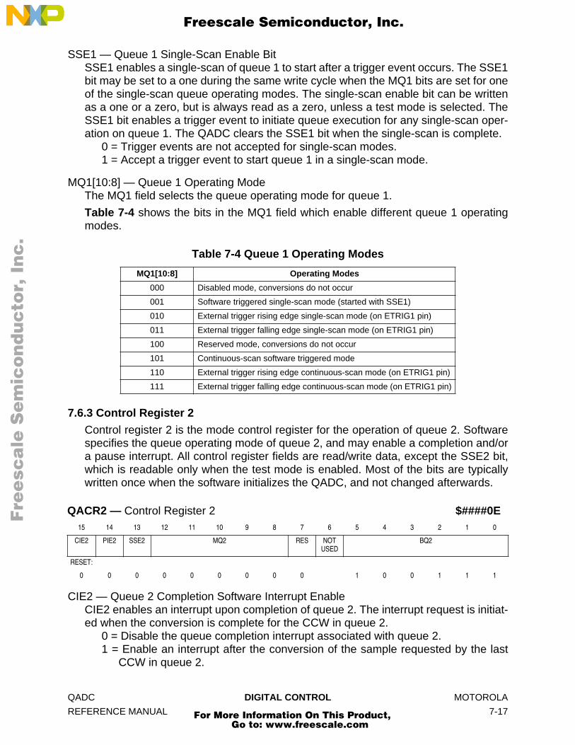
F
ree
sca
le S
em
ico
nd
uc
tor,
I
Freescale Semiconductor, Inc.n
c..
.
SSE1 — Queue 1 Single-Scan Enable BitSSE1 enables a single-scan of queue 1 to start after a trigger event occurs. The SSE1bit may be set to a one during the same write cycle when the MQ1 bits are set for oneof the single-scan queue operating modes. The single-scan enable bit can be writtenas a one or a zero, but is always read as a zero, unless a test mode is selected. TheSSE1 bit enables a trigger event to initiate queue execution for any single-scan oper-ation on queue 1. The QADC clears the SSE1 bit when the single-scan is complete.
0 = Trigger events are not accepted for single-scan modes.1 = Accept a trigger event to start queue 1 in a single-scan mode.
MQ1[10:8] — Queue 1 Operating ModeThe MQ1 field selects the queue operating mode for queue 1.
Table 7-4 shows the bits in the MQ1 field which enable different queue 1 operatingmodes.
7.6.3 Control Register 2
Control register 2 is the mode control register for the operation of queue 2. Softwarespecifies the queue operating mode of queue 2, and may enable a completion and/ora pause interrupt. All control register fields are read/write data, except the SSE2 bit,which is readable only when the test mode is enabled. Most of the bits are typicallywritten once when the software initializes the QADC, and not changed afterwards.
CIE2 — Queue 2 Completion Software Interrupt EnableCIE2 enables an interrupt upon completion of queue 2. The interrupt request is initiat-ed when the conversion is complete for the CCW in queue 2.
0 = Disable the queue completion interrupt associated with queue 2.1 = Enable an interrupt after the conversion of the sample requested by the last
CCW in queue 2.
Table 7-4 Queue 1 Operating Modes
MQ1[10:8] Operating Modes
000 Disabled mode, conversions do not occur
001 Software triggered single-scan mode (started with SSE1)
010 External trigger rising edge single-scan mode (on ETRIG1 pin)
011 External trigger falling edge single-scan mode (on ETRIG1 pin)
100 Reserved mode, conversions do not occur
101 Continuous-scan software triggered mode
110 External trigger rising edge continuous-scan mode (on ETRIG1 pin)
111 External trigger falling edge continuous-scan mode (on ETRIG1 pin)
QACR2 — Control Register 2 $####0E15 14 13 12 11 10 9 8 7 6 5 4 3 2 1 0
CIE2 PIE2 SSE2 MQ2 RES NOT USED
BQ2
RESET:
0 0 0 0 0 0 0 0 0 1 0 0 1 1 1
QADC DIGITAL CONTROL MOTOROLA
REFERENCE MANUAL 7-17
For More Information On This Product, Go to: www.freescale.com

F
ree
sca
le S
em
ico
nd
uc
tor,
I
Freescale Semiconductor, Inc.n
c..
.
PIE2 — Queue 2 Pause Software Interrupt EnablePIE2 enables an interrupt when queue 2 enters the pause state. The interrupt requestis initiated when conversion is complete for a CCW that has the pause bit set.
0 = Disable the pause interrupt associated with queue 2.1 = Enable an interrupt after the conversion of the sample requested by a CCW in
queue 2 which has the pause bit set.
SSE2 — Queue 2 Single-Scan Enable BitSSE2 enables a single-scan of queue 2 to start after a trigger event occurs. The SSE2bit may be set to a one during the same write cycle when the MQ2 bits are set for oneof the single-scan queue operating modes. The single-scan enable bit can be writtenas a one or a zero, but is always read as a zero, unless a test mode is selected. TheSSE2 bit enables a trigger event to initiate queue execution for any single-scan oper-ation on queue 2. The QADC clears the SSE2 bit when the single-scan is complete.
0 = Trigger events are not accepted for single-scan modes.1 = Accept a trigger event to start queue 2 in a single-scan mode.
MQ2[12:8] — Queue 2 Operating ModeThe MQ2 field selects the queue operating mode for queue 2.
Table 7-5 shows the bits in the MQ2 field which enable different queue 2 operatingmodes.
Table 7-5 Queue 2 Operating Modes
MQ2[12:8] Operating Modes
00000 Disabled mode, conversions do not occur00001 Software triggered single-scan mode (started with SSE2)00010 External trigger rising edge single-scan mode (on ETRIG2 pin)00011 External trigger falling edge single-scan mode (on ETRIG2 pin)00100 Interval timer single-scan mode: time = QCLK period x 27
00101 Interval timer single-scan mode: time = QCLK period x 28
00110 Interval timer single-scan mode: time = QCLK period x 29
00111 Interval timer single-scan mode: time = QCLK period x 210
01000 Interval timer single-scan mode: time = QCLK period x 211
01001 Interval timer single-scan mode: time = QCLK period x 212
01010 Interval timer single-scan mode: time = QCLK period x 213
01011 Interval timer single-scan mode: time = QCLK period x 214
01100 Interval timer single-scan mode: time = QCLK period x 215
01101 Interval timer single-scan mode: time = QCLK period x 216
01110 Interval timer single-scan mode: time = QCLK period x 217
01111 Reserved mode10000 Reserved mode10001 Continuous-scan software triggered mode10010 External trigger rising edge continuous-scan mode (on ETRIG2 pin)10011 External trigger falling edge continuous-scan mode (on ETRIG2 pin)10100 Periodic timer continuous-scan mode: time = QCLK period x 27
10101 Periodic timer continuous-scan mode: time = QCLK period x 28
MOTOROLA DIGITAL CONTROL QADC
7-18 REFERENCE MANUAL
For More Information On This Product, Go to: www.freescale.com

F
ree
sca
le S
em
ico
nd
uc
tor,
I
Freescale Semiconductor, Inc.n
c..
.
RES — Queue 2 Resume
RES selects the queue 2 resumption point after suspension due to queue 1. If RES ischanged during the execution of queue 2, the change is not recognized until an end-of-queue condition is reached, or the queue operating mode of queue 2 is changed.
The primary reason for selecting re-execution of the entire queue or subqueue is toguarantee that all samples are taken consecutively in one scan (coherency).
When subqueues are not used, queue 2 execution restarts after suspension with thefirst CCW in queue 2. When a pause has previously occurred in queue 2 execution,queue execution restarts after suspension with the first CCW in the current subqueue.
A subqueue is considered to be a stand-alone sequence of conversions. Once apause flag has been set to report subqueue completion, that subqueue is not repeateduntil all CCWs in queue 2 are executed.
An example of using the resume bit is when the frequency of queue 1 trigger eventsprohibit queue 2 completion. If the rate of queue 1 execution is too high, it is best forqueue 2 execution to continue with the CCW that was being converted when queue 2was suspended. This allows queue 2 to eventually complete execution.
0 = After suspension, begin execution with the first CCW in queue 2 or the currentsubqueue.
1 = After suspension, begin execution with the aborted CCW in queue 2.
BQ2[5:0] — Beginning of Queue 2
The BQ2 field indicates the CCW location where queue 2 begins. To allow the lengthof queue 1 and queue 2 to vary, a programmable pointer identifies the CCW table lo-cation where queue 2 begins. The BQ2 field also serves as an end-of-queue conditionfor queue 1.
Software defines the beginning of queue 2 by programming the BQ2 field in QACR2.BQ2 is usually programmed before or at the same time as the queue operating modefor queue 2 is selected. If BQ2 is 40 or greater, queue 2 does not have any entries,and the entire CCW table is dedicated to queue 1. If BQ2 is 0, the entire CCW table is
10110 Periodic timer continuous-scan mode: time = QCLK period x 29
10111 Periodic timer continuous-scan mode: time = QCLK period x 210
11000 Periodic timer continuous-scan mode: time = QCLK period x 211
11001 Periodic timer continuous-scan mode: time = QCLK period x 212
11010 Periodic timer continuous-scan mode: time = QCLK period x 213
11011 Periodic timer continuous-scan mode: time = QCLK period x 214
11100 Periodic timer continuous-scan mode: time = QCLK period x 215
11101 Periodic timer continuous-scan mode: time = QCLK period x 216
11110 Periodic timer continuous-scan mode: time = QCLK period x 217
11111 Reserved mode
Table 7-5 Queue 2 Operating Modes (Continued)
MQ2[12:8] Operating Modes
QADC DIGITAL CONTROL MOTOROLA
REFERENCE MANUAL 7-19
For More Information On This Product, Go to: www.freescale.com
F
ree
sca
le S
em
ico
nd
uc
tor,
I
Freescale Semiconductor, Inc.n
c..
.
dedicated to queue 2. As a special case, when a queue operating mode for queue 1is selected and a trigger event occurs for queue 1 with BQ2 set to 0, queue 1 executionis terminated after CCW0 is read. Conversions do not occur.
The BQ2 pointer may be changed dynamically, to alternate between queue 2 scan se-quences. A change in BQ2 while queue 2 is active does not take effect until an end-of-queue condition is recognized, or until the queue operating mode of queue 2 ischanged. For example, two scan sequences could be defined as follows: the first se-quence starts at CCW10, with a pause after CCW11 and an EOQ programmed inCCW15; the second sequence starts at CCW16, with a pause after CCW17 and anEOQ programmed in CCW39.
With BQ2 set to CCW10 and the continuous-scan mode selected, queue executionbegins. When the pause is encountered in CCW11, a software interrupt routine canredefine BQ2 to be CCW16. Therefore, after the end-of-queue is recognized inCCW15, an internal retrigger event is generated and execution restarts at CCW16.When the pause software interrupt occurs again, software can change BQ2 back toCCW10. After the end-of-queue is recognized in CCW39, an internal retrigger eventis created and execution now restarts at CCW10.
If BQ2 is changed while queue 1 is active, the effect of BQ2 as an end-of-queue indi-cation for queue 1 is immediate.
NOTE
If BQ2 was assigned to the CCW that queue 1 is currently workingon, then that conversion is completed before BQ2 takes effect.
Each time a CCW is read for queue 1, the CCW location is compared with the currentvalue of the BQ2 pointer to detect a possible end-of-queue condition. For example, ifBQ2 is changed to CCW3 while queue 1 is converting CCW2, queue 1 is terminatedafter the conversion is completed. However, if BQ2 is changed to CCW1 while queue1 is converting CCW2, the QADC would not recognize a BQ2 end-of-queue conditionuntil queue 1 execution reached CCW1 again, presumably on the next pass throughthe queue.
7.6.4 Status Register
The status register contains information about the state of each queue and the currentA/D conversion. Except for the four flag bits (CF1, PF1, CF2, and PF2) and the twotrigger overrun bits (TOR1 and TOR2), all of the status register fields contain read-onlydata. The four flag bits and the two trigger overrun bits are cleared by writing a zero tothe bit after the bit was previously read as a one.
QASR — Status Register $####1015 14 13 12 11 10 9 8 7 6 5 4 3 2 1 0
CF1 PF1 CF2 PF2 TOR1 TOR2 QS CWP
RESET:
0 0 0 0 0 0 0 0 0 0 0 0 0 0 0 0
MOTOROLA DIGITAL CONTROL QADC
7-20 REFERENCE MANUAL
For More Information On This Product, Go to: www.freescale.com
F
ree
sca
le S
em
ico
nd
uc
tor,
I
Freescale Semiconductor, Inc.n
c..
.
CF1 — Queue 1 Completion FlagCF1 indicates that a queue 1 scan has been completed. The scan completion flag isset by the QADC when the input channel sample requested by the last CCW in queue1 is converted, and the result is stored in the result table.
The end of queue 1 is identified when execution is complete on the CCW in the loca-tion prior to that pointed to by BQ2, when the current CCW contains an end-of-queuecode instead of a valid channel number, or when the currently completed CCW is inthe last location of the CCW RAM.
When CF1 is set and interrupts are enabled for that queue completion flag, the QADCasserts an interrupt request at the level specified by IRL1 in the interrupt register(QADCINT). The software reads the completion flag during an interrupt service routineto identify the interrupt request. The interrupt request is cleared when the softwarewrites a zero to the completion flag bit, when the bit was previously read as a one.Once set, only software or reset can clear CF1.
CF1 is maintained by the QADC regardless of whether the corresponding interrupt isenabled. The software polls for CF1 bit to see if it is set. This allows the software torecognize that the QADC is finished with a queue 1 scan. The software acknowledgesthat it has detected the completion flag being set by writing a zero to the completionflag after the bit was read as a one.
Refer to SECTION 8 INTERRUPTS for more information. 0 = Queue 1 scan is not complete.1 = Queue 1 scan is complete.
PF1 — Queue 1 Pause FlagPF1 indicates that a queue 1 scan has reached a pause. PF1 is set by the QADC whenthe current queue 1 CCW has the pause bit set, the selected input channel has beenconverted, and the result has been stored in the result table.
Once PF1 is set, the queue enters the paused state and waits for a trigger event toallow queue execution to continue. However, if the CCW with the pause bit set is thelast CCW in a queue, the queue execution is complete. The queue status becomesidle, not paused, and both the pause and completion flags are set.
When PF1 is set and interrupts are enabled for the corresponding queue, the QADCasserts an interrupt request at the level specified by IRL1 in the interrupt register. Thesoftware may read PF1 during an interrupt service routine to identify the interrupt re-quest. The interrupt request is cleared when the software writes a zero to PF1, whenthe bit was previously read as a one. Once set, only software or reset can clear PF1.
PF1 is maintained by the QADC regardless of whether the corresponding interruptsare enabled. The software may poll PF1 to find out when the QADC has reached apause in scanning a queue. The software acknowledges that it has detected a pauseflag being set by writing a zero to PF1 after the bit was last read as a one.
0 = Queue 1 has not reached a pause.1 = Queue 1 has reached a pause.
QADC DIGITAL CONTROL MOTOROLA
REFERENCE MANUAL 7-21
For More Information On This Product, Go to: www.freescale.com

F
ree
sca
le S
em
ico
nd
uc
tor,
I
Freescale Semiconductor, Inc.n
c..
.
CF2 — Queue 2 Completion FlagCF2 indicates that a queue 2 scan has been completed. CF2 is set by the QADC whenthe input channel sample requested by the last CCW in queue 2 is converted, and theresult is stored in the result table.
The end of queue 2 is identified when the current CCW contains an end-of-queue codeinstead of a valid channel number, or when the currently completed CCW is in the lastlocation of the CCW RAM.
When CF2 is set and interrupts are enabled for that queue completion flag, the QADCasserts an interrupt request at the level specified by IRL2 in the interrupt register(QADCINT). The software reads CF2 during an interrupt service routine to identify theinterrupt request. The interrupt request is cleared when the software writes a zero tothe CF2 bit, when the bit was previously read as a one. Once set, only software or re-set can clear CF2.
CF2 is maintained by the QADC regardless of whether the corresponding interruptsare enabled. The software polls for CF2 to see if it is set. This allows the software torecognize that the QADC is finished with a queue 2 scan. The software acknowledgesthat it has detected the completion flag being set by writing a zero to the completionflag after the bit was read as a one.
Refer to SECTION 8 INTERRUPTS for more information. 0 = Queue 2 scan is not complete.1 = Queue 2 scan is complete.
PF2 — Queue 2 Pause FlagPF2 indicates that a queue 2 scan has reached a pause. PF2 is set by the QADC whenthe current queue 2 CCW has the pause bit set, the selected input channel has beenconverted, and the result has been stored in the result table.
Once PF2 is set, the queue enters the paused state and waits for a trigger event toallow queue execution to continue. However, if the CCW with the pause bit set is thelast CCW in a queue, the queue execution is complete. The queue status becomesidle, not paused, and both the pause and completion flags are set.
When PF2 is set and interrupts are enabled for the corresponding queue, the QADCasserts an interrupt request at the level specified by IRL2 in the interrupt register. Thesoftware reads PF2 during an interrupt service routine to identify the interrupt request.The interrupt request is cleared when the software writes a zero to PF2, when the bitwas previously read as a one. Once set, only software or reset can clear PF2.
PF2 is maintained by the QADC regardless of whether the corresponding interruptsare enabled. The software may poll PF2 to find out when the QADC has reached apause in scanning a queue. The software acknowledges that it has detected a pauseflag being set by writing a zero to PF2 after the bit was last read as a one.
0 = Queue 2 has not reached a pause.1 = Queue 2 has reached a pause.
MOTOROLA DIGITAL CONTROL QADC
7-22 REFERENCE MANUAL
For More Information On This Product, Go to: www.freescale.com

F
ree
sca
le S
em
ico
nd
uc
tor,
I
Freescale Semiconductor, Inc.n
c..
.
TOR1 — Queue 1 Trigger OverrunTOR1 indicates that an unexpected trigger event has occurred for queue 1. TOR1 canbe set only while queue 1 is in the active state.
A trigger event generated by a transition on the external trigger pin or by the periodic/interval timer may be recorded as a trigger overrun. TOR1 can only occur when usingan external trigger mode. TOR1 cannot occur when the software initiated single-scanmode and the software initiated continuous-scan mode are selected.
TOR1 occurs when a trigger event is received while a queue is executing and beforethe scan has completed or paused. TOR1 can also occur when a trigger event has oc-curred on a queue, but execution has not yet begun. TOR1 has no effect on the queueexecution.
After a trigger event has occurred for queue 1, and before the scan has completed orpaused, additional queue 1 trigger events are not retained. Such trigger events areconsidered unexpected, and the QADC sets the TOR1 error status bit. An unexpectedtrigger event may be a system overrun situation, indicating a system loading mis-match. The software acknowledges that it has detected a trigger overrun being set bywriting a zero to the trigger overrun, after the bit was read as a one. Once set, onlysoftware or reset can clear TOR1.
0 = No unexpected queue 1 trigger events have occurred.1 = At least one unexpected queue 1 trigger event has occurred.
TOR2 — Queue 2 Trigger OverrunTOR2 indicates that an unexpected trigger event has occurred for queue 2. TOR2 canbe set when queue 2 is in the active, suspended, and trigger pending states.
The TOR2 trigger overrun can only occur when using an external trigger mode or aperiodic/interval timer mode. Trigger overruns cannot occur when the software initiat-ed single-scan mode and the software initiated continuous-scan mode are selected.
TOR2 occurs when a trigger event is received while a queue is executing and beforethe scan has completed or paused. TOR2 also occurs when a trigger event has oc-curred on a queue, but execution has not yet begun. TOR2 has no effect on the queueexecution. A trigger event that causes a trigger overrun is not retained since it is con-sidered unexpected.
After a trigger event has occurred for queue 2, and before the scan has completed orpaused, additional queue 2 trigger events are not retained, and are considered unex-pected. Also, when a queue 2 trigger event is pending, but queue 1 is active, additionalqueue 2 trigger events are considered unexpected. In both cases, the QADC sets theTOR2 error status bit.
An unexpected trigger event may be a system overrun situation, indicating a systemloading mismatch. The software acknowledges that it has detected a trigger overrunbeing set by writing a zero to the trigger overrun, after the bit was read as a one. Onceset, only software or reset can clear TOR2.
0 = No unexpected queue 2 trigger events have occurred.1 = At least one unexpected queue 2 trigger event has occurred.
QADC DIGITAL CONTROL MOTOROLA
REFERENCE MANUAL 7-23
For More Information On This Product, Go to: www.freescale.com

F
ree
sca
le S
em
ico
nd
uc
tor,
I
Freescale Semiconductor, Inc.n
c..
.
QS[9:6] — Queue StatusThe 4-bit read-only QS field indicates the current condition of queue 1 and queue 2.The following are the five queue status conditions:
• Idle• Active• Paused• Suspended• Trigger pending
The two most significant bits are associated primarily with queue 1, and the remainingtwo bits are associated with queue 2. Since the priority scheme between the twoqueues causes the status to be interlinked, the status bits are considered as one 4-bitfield.
Table 7-6 shows the bits in the QS field and how they affect the status of queue 1 andqueue 2. Refer to SECTION 9 QUEUE PRIORITY EXAMPLES, which shows the 4-bitqueue status field transitions in typical situations.
One or both queues may be in the idle state. When a queue is idle, CCWs are not be-ing executed for that queue, the queue is not in the pause state, and there is not a trig-ger pending.
The idle state occurs when a queue is disabled, when a queue is in a reserved mode,or when a queue is in a valid queue operating mode awaiting a trigger event to initiatequeue execution.
A queue is in the active state when a valid queue operating mode is selected, whenthe selected trigger event has occurred, or when the QADC is performing a conversionspecified by a CCW from that queue.
Table 7-6 Queue Status
QS[9:6] Queue 1/Queue 2 States
0000 Queue 1 idle, Queue 2 idle
0001 Queue 1 idle, Queue 2 paused
0010 Queue 1 idle, Queue 2 active
0011 Queue 1 idle, Queue 2 trigger pending
0100 Queue 1 paused, Queue 2 idle
0101 Queue 1 paused, Queue 2 paused
0110 Queue 1 paused, Queue 2 active
0111 Queue 1 paused, Queue 2 trigger pending
1000 Queue 1 active, Queue 2 idle
1001 Queue 1 active, Queue 2 paused
1010 Queue 1 active, Queue 2 suspended
1011 Queue 1 active, Queue 2 trigger pending
1100 Reserved
1101 Reserved
1110 Reserved
1111 Reserved
MOTOROLA DIGITAL CONTROL QADC
7-24 REFERENCE MANUAL
For More Information On This Product, Go to: www.freescale.com
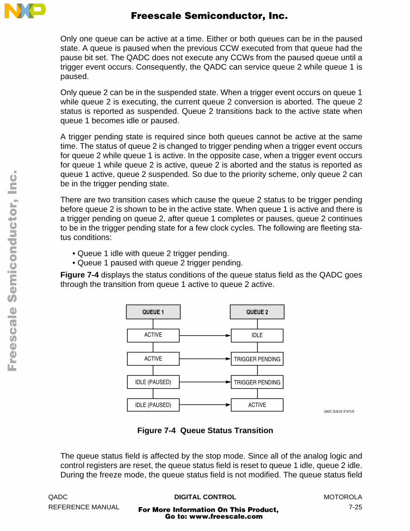
F
ree
sca
le S
em
ico
nd
uc
tor,
I
Freescale Semiconductor, Inc.n
c..
.
Only one queue can be active at a time. Either or both queues can be in the pausedstate. A queue is paused when the previous CCW executed from that queue had thepause bit set. The QADC does not execute any CCWs from the paused queue until atrigger event occurs. Consequently, the QADC can service queue 2 while queue 1 ispaused.
Only queue 2 can be in the suspended state. When a trigger event occurs on queue 1while queue 2 is executing, the current queue 2 conversion is aborted. The queue 2status is reported as suspended. Queue 2 transitions back to the active state whenqueue 1 becomes idle or paused.
A trigger pending state is required since both queues cannot be active at the sametime. The status of queue 2 is changed to trigger pending when a trigger event occursfor queue 2 while queue 1 is active. In the opposite case, when a trigger event occursfor queue 1 while queue 2 is active, queue 2 is aborted and the status is reported asqueue 1 active, queue 2 suspended. So due to the priority scheme, only queue 2 canbe in the trigger pending state.
There are two transition cases which cause the queue 2 status to be trigger pendingbefore queue 2 is shown to be in the active state. When queue 1 is active and there isa trigger pending on queue 2, after queue 1 completes or pauses, queue 2 continuesto be in the trigger pending state for a few clock cycles. The following are fleeting sta-tus conditions:
• Queue 1 idle with queue 2 trigger pending.• Queue 1 paused with queue 2 trigger pending.
Figure 7-4 displays the status conditions of the queue status field as the QADC goesthrough the transition from queue 1 active to queue 2 active.
Figure 7-4 Queue Status Transition
The queue status field is affected by the stop mode. Since all of the analog logic andcontrol registers are reset, the queue status field is reset to queue 1 idle, queue 2 idle.During the freeze mode, the queue status field is not modified. The queue status field
QUEUE 1 QUEUE 2
TRIGGER PENDING
TRIGGER PENDING
ACTIVE
IDLEACTIVE
ACTIVE
IDLE (PAUSED)
IDLE (PAUSED)
QADC QUEUE STATUS
QADC DIGITAL CONTROL MOTOROLA
REFERENCE MANUAL 7-25
For More Information On This Product, Go to: www.freescale.com

F
ree
sca
le S
em
ico
nd
uc
tor,
I
Freescale Semiconductor, Inc.n
c..
.
retains the status it held prior to freezing. As a result, the queue status can show queue1 active, queue 2 idle, even though neither queue is being executed during freeze.
CWP — Command Word PointerThe CWP allows the software to know which CCW is executing at present, or was lastcompleted. The command word pointer is a software read-only field, and write opera-tions have no effect. The CWP allows software to monitor the progress of the QADCscan sequence. The CWP field is a CCW word pointer with a valid range of 0 to 39.
When a queue enters the paused state, the CWP points to the CCW with the pausebit set. While in pause, the CWP value is maintained until a trigger event occurs on thesame queue or the other queue. Usually, the CWP is updated a few clock cycles be-fore the queue status field shows that the queue has become active. For example,software may read a CWP pointing to a CCW in queue 2, and the status field showsqueue 1 paused, queue 2 trigger pending.
When the QADC finishes the scan of the queue, the CWP points to the CCW wherethe end-of-queue condition was detected. Therefore, when the end-of-queue conditionis a CCW with the EOQ code (channel 63), the CWP points to the CCW containing theEOQ.
When the last CCW in a queue is in the last CCW table location (CCW39), and it doesnot contain the EOQ code, the end-of-queue is detected when the following CCW isread, so the CWP points to word 40.
Finally, when queue 1 operation is terminated after a CCW is read that is defined asBQ2, the CWP points to the same CCW as BQ2.
Since the CWP is six bits, the value could range from 0 to 63. However, since thereare 40 locations in the CCW table, the normal range of CWP is 0 to 39. The CWPshows 40 when queue execution terminates with the physical end of the CCW table.The CWP would also show a value between 40 and 63 if BQ2 were set in that rangeand queue 2 execution were initiated.
During the stop mode, the CWP is reset to zero, since the control registers and theanalog logic are reset. When the freeze mode is entered, the CWP is unchanged; itpoints to the last executed CCW.
7.7 Conversion Command Word Table
The CCW table is a RAM, 40 words long and 10 bits wide, which can be programmedby the software to request conversions of one or more analog input channels. The en-tries in the CCW table are 10-bit conversion command words. The CCW table is writ-ten by software and is not modified by the QADC. Each CCW requests the conversionof an analog channel to a digital result. The CCW specifies the analog channel num-ber, the input sample time, and whether the queue is to pause after the current CCW.The ten implemented bits of the CCW word are read/write data, but they may be writ-ten once when the software initializes the QADC, and not changed afterwards. Unim-plemented bits are read as zeros, and write operations have no effect. Each locationin the CCW table corresponds to a location in the result word table. When a conversion
MOTOROLA DIGITAL CONTROL QADC
7-26 REFERENCE MANUAL
For More Information On This Product, Go to: www.freescale.com

F
ree
sca
le S
em
ico
nd
uc
tor,
I
Freescale Semiconductor, Inc.n
c..
.
is completed for a CCW entry, the 10-bit result is written in the corresponding resultword entry. The QADC provides 40 CCW table entries. If more results are needed,software uses one or more result table locations for multiple channels.
The beginning of queue 1 is the first location in the CCW table. The first location ofqueue 2 is specified by the beginning of queue 2 pointer (BQ2) in QACR2. To dedicatethe entire CCW table to queue 1, queue 2 is programmed to be in the disabled mode,and the beginning of BQ2 is programmed to any value greater than 39. To dedicatethe entire CCW table to queue 2, queue 1 is programmed to be in the disabled mode,and BQ2 is specified as the first location in the CCW table.
Figure 7-5 illustrates the operation of the queue structure.
Figure 7-5 QADC Conversion Queue Operation
QADC CQ
00 BEGIN QUEUE 1
BQ2
39
END OF QUEUE 1
BEGIN QUEUE 2
END OF QUEUE 2
P IST CHAN
9 78 6 4 3 2 15 0
P = PAUSE UNTIL NEXT TRIGGER
IST = INPUT SAMPLE TIMECHAN = CHANNEL NUMBER AND END-OF-QUEUE CODE
10-BIT CONVERSION COMMANDWORD FORMAT
00
39
RESULT
78 6 4 3 2 159 08101112131415
RESULT
9 78 4 3 2 15 081011121314 615
S RESULT
9 78 4 3 2 15 081011121314 615
0000000
000000
000000
RIGHT JUSTIFIED, UNSIGNED RESULT
LEFT JUSTIFIED, UNSIGNED RESULT
LEFT JUSTIFIED, SIGNED RESULT
10-BIT RESULT, READABLE IN THREE 16-BIT FORMATS
S = SIGN BIT
CHANNEL SELECT,SAMPLE, HOLD, AND
A/D CONVERSION
CONVERSION COMMAND WORD(CCW) TABLE
RESULT WORD TABLE
BYP
BYP = BYPASS
QADC DIGITAL CONTROL MOTOROLA
REFERENCE MANUAL 7-27
For More Information On This Product, Go to: www.freescale.com

F
ree
sca
le S
em
ico
nd
uc
tor,
I
Freescale Semiconductor, Inc.n
c..
.
To prepare the QADC for a scan sequence, the software writes to the CCW table tospecify the desired channel conversions. The software also establishes the criteria forinitiating the queue execution by programming the queue operating mode. The queueoperating mode determines what type of trigger event causes queue execution to be-gin. “Trigger event” is used to refer to any of the ways to cause the QADC to beginexecuting the CCWs in a queue or subqueue. An “external trigger” is only one of thepossible “trigger events”.
A scan sequence may be initiated by the following:
• A software command• Expiration of the periodic/interval timer• External trigger signal
The software also specifies whether the QADC is to perform a single pass through thequeue or is to scan continuously. When a single-scan mode is selected, the softwareselects the queue operating mode and sets the single-scan enable bit. When a contin-uous-scan mode is selected, the queue remains active in the selected queue operat-ing mode after the QADC completes each queue scan sequence.
During queue execution, the QADC reads each CCW from the active queue and exe-cutes conversions in four stages:
• Initial sample• Transfer• Final sample• Resolution
During initial sample, the selected input channel is connected to the sample capacitorat the input of the sample buffer amplifier.
During the transfer period, the sample capacitor is disconnected from the multiplexer,and the stored voltage is buffered and transferred to the RC DAC array.
During the final sample period, the sample capacitor and amplifier are bypassed, andthe multiplexer input charges the RC DAC array directly. Each CCW specifies a finalinput sample time of 2, 4, 8, or 16 QCLK cycles. When an analog-to-digital conversionis complete, the result is written to the corresponding location in the result word table.The QADC continues to sequentially execute each CCW in the queue until the end ofthe queue is detected or a pause bit is found in a CCW.
When the pause bit is set in the current CCW, the QADC stops execution of the queueuntil a new trigger event occurs. The pause status flag bit is set, which may cause aninterrupt to notify the software that the queue has reached the pause state. After thetrigger event occurs, the paused state ends and the QADC continues to execute eachCCW in the queue until another pause is encountered or the end of the queue is de-tected.
The following indicate the end-of-queue condition:
• The CCW channel field is programmed with 63 ($3F) to specify the end of thequeue.
MOTOROLA DIGITAL CONTROL QADC
7-28 REFERENCE MANUAL
For More Information On This Product, Go to: www.freescale.com

F
ree
sca
le S
em
ico
nd
uc
tor,
I
Freescale Semiconductor, Inc.n
c..
.
• The end of queue 1 is implied by the beginning of queue 2, which is specified inthe BQ2 field in QACR2.
• The physical end of the queue RAM space defines the end of either queue.
When any of the end-of-queue conditions is recognized, a queue completion flag isset, and if enabled, an interrupt is issued to the software. The following situations pre-maturely terminate queue execution:
• Since queue 1 is higher in priority than queue 2, when a trigger event occurs onqueue 1 during queue 2 execution, the execution of queue 2 is suspended byaborting the execution of the CCW in progress, and the queue 1 execution be-gins. When queue 1 execution is completed, queue 2 conversions restart with thefirst CCW entry in queue 2 or the first CCW of the queue 2 subqueue being exe-cuted when queue 2 was suspended. Alternately, conversions can restart with theaborted queue 2 CCW entry. The resume (RES) field in QACR2 allows the soft-ware to select where queue 2 begins after suspension. By choosing to re-executeall of the suspended queue 2 queue and subqueue CCWs, all of the samples areguaranteed to have been taken during the same scan pass. However, a high trig-ger event rate for queue 1 can prohibit the completion of queue 2. If this occurs,the software may choose to begin execution of queue 2 with the aborted CCWentry.
• Software can change the queue operating mode to disabled mode. Any currentconversion taking place for that queue is aborted. Putting a queue into the dis-abled mode does not power down the converter.
• Software can change the queue operating mode to another valid mode. Any cur-rent conversion taking place for that queue is aborted. The queue restarts at thebeginning of the queue, once an appropriate trigger event occurs.
• For low power operation, software can set the stop mode bit to prepare the mod-ule for a loss of clocks. The QADC aborts any conversion in progress when thestop mode is entered.
• When the freeze enable bit is set by software and the IMB internal FREEZE lineis asserted, the QADC freezes at the end of the current conversion. When internalFREEZE is negated, the QADC resumes queue execution beginning with the nextCCW entry. Refer to paragraph 3.3.2 in SECTION 3 CONFIGURATION ANDCONTROL for more information.
P — PauseThe pause bit allows software to create sub-queues within queue 1 and queue 2. TheQADC performs the conversion specified by the CCW with the pause bit set, and thenthe queue enters the pause state. Another trigger event causes execution to continuefrom the pause to the next CCW.
0 = Do not enter the pause state after execution of the current CCW.1 = Enter the pause state after execution of the current CCW.
CCW — Conversion Command Word Table $####30–$####7E15 14 13 12 11 10 9 8 7 6 5 4 3 2 1 0
NOT USED P BYP IST CHAN
RESET:
U U U U U U U U U U
QADC DIGITAL CONTROL MOTOROLA
REFERENCE MANUAL 7-29
For More Information On This Product, Go to: www.freescale.com
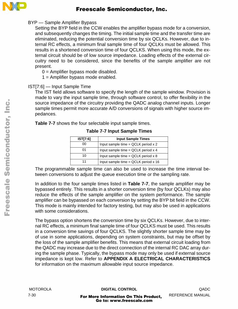
F
ree
sca
le S
em
ico
nd
uc
tor,
I
Freescale Semiconductor, Inc.n
c..
.
BYP — Sample Amplifier BypassSetting the BYP field in the CCW enables the amplifier bypass mode for a conversion,and subsequently changes the timing. The initial sample time and the transfer time areeliminated, reducing the potential conversion time by six QCLKs. However, due to in-ternal RC effects, a minimum final sample time of four QCLKs must be allowed. Thisresults in a shortened conversion time of four QCLKS. When using this mode, the ex-ternal circuit should be of low source impedance. Loading effects of the external cir-cuitry need to be considered, since the benefits of the sample amplifier are notpresent.
0 = Amplifier bypass mode disabled.1 = Amplifier bypass mode enabled.
IST[7:6] — Input Sample TimeThe IST field allows software to specify the length of the sample window. Provision ismade to vary the input sample time, through software control, to offer flexibility in thesource impedance of the circuitry providing the QADC analog channel inputs. Longersample times permit more accurate A/D conversions of signals with higher source im-pedances.
Table 7-7 shows the four selectable input sample times.
The programmable sample time can also be used to increase the time interval be-tween conversions to adjust the queue execution time or the sampling rate.
In addition to the four sample times listed in Table 7-7, the sample amplifier may bebypassed entirely. This results in a shorter conversion time (by four QCLKs) may alsoreduce the effects of the sample amplifier on the system performance. The sampleamplifier can be bypassed on each conversion by setting the BYP bit field in the CCW.This mode is mainly intended for factory testing, but may also be used in applicationswith some considerations.
The bypass option shortens the conversion time by six QCLKs. However, due to inter-nal RC effects, a minimum final sample time of four QCLKS must be used. This resultsin a conversion time savings of four QCLKS. The slightly shorter sample time may beof use in some applications, depending on system constraints, but may be offset bythe loss of the sample amplifier benefits. This means that external circuit loading fromthe QADC may increase due to the direct connection of the internal RC DAC array dur-ing the sample phase. Typically, the bypass mode may only be used if external sourceimpedance is kept low. Refer to APPENDIX A ELECTRICAL CHARACTERISTICSfor information on the maximum allowable input source impedance.
Table 7-7 Input Sample Times
IST[7:6] Input Sample Times00 Input sample time = QCLK period x 2
01 Input sample time = QCLK period x 4
10 Input sample time = QCLK period x 8
11 Input sample time = QCLK period x 16
MOTOROLA DIGITAL CONTROL QADC
7-30 REFERENCE MANUAL
For More Information On This Product, Go to: www.freescale.com

F
ree
sca
le S
em
ico
nd
uc
tor,
I
Freescale Semiconductor, Inc.n
c..
.
CHAN[5:0] — Channel NumberThe CHAN field selects the input channel number. The software programs the channelfield of the CCW with the channel number corresponding to the analog input pin to besampled and converted. The analog input pin channel number assignments and thepin definitions vary depending on whether the multiplexed or non-multiplexed mode isused by the application. As far as the queue scanning operations are concerned, thereis no distinction between an internally or externally multiplexed analog input. Refer toSECTION 4 EXTERNAL MULTIPLEXING for more information on external multiplex-ing.
Table 7-8 shows the channel number assignments for the nonmultiplexed mode. Ta-ble 7-9 shows the channel number assignments for the multiplexed mode.
Table 7-8 Nonmultiplexed Channel Assignments and Pin Designations
Nonmultiplexed Input Pins Channel Number in CCW CHAN Field
Port Pin Name
Analog Pin Name
Other Functions
Pin Type Binary Decimal
PQB0PQB1PQB2PQB3
AN0AN1AN2AN3
————
InputInputInputInput
000000000001000010000011
0123
——
PQB4PQB5
——
AN48AN49
InvalidReserved
——
——
InputInput
0XXXXX10XXXX110000110001
4 to 3132 to 47
4849
PQB6PQB7PQA0PQA1
AN50AN51AN52AN53
————
InputInput
Input/OutputInput/Output
110010110011110100110101
50515253
PQA2PQA3PQA4PQA5
AN54AN55AN56AN57
—ETRIG1ETRIG2
—
Input/OutputInput/OutputInput/OutputInput/Output
110110110111111000111001
54555657
PQA6PQA7VRLVRH
AN58AN59
Low RefHigh Ref
————
Input/OutputInput/Output
InputInput
111010111011111100111101
58596061
——
——
VDDA/2End of Queue Code
——
111110111111
6263
QADC DIGITAL CONTROL MOTOROLA
REFERENCE MANUAL 7-31
For More Information On This Product, Go to: www.freescale.com

F
ree
sca
le S
em
ico
nd
uc
tor,
I
Freescale Semiconductor, Inc.n
c..
.
If the CCW channel field specifies a reserved channel number (channels 32 to 47) oran invalid channel number (channels 4 to 31 in the non-multiplexed mode), the low ref-erence level (VRL) is converted. The channel field is programmed for channel 63 to in-dicate the end of the queue. Channels 60 to 63 are special internal channels. Whenone of the special channels is selected, the sampling amplifier is not used. The valueof VRL, VRH, or VDDA/2 is placed directly onto the converter. Also for the internal spe-cial channels, programming any input sample time other than two has no benefit ex-cept to lengthen the overall conversion time.
7.8 Result Word Table
The result word table is a RAM, 40 words long and 10 bits wide. An entry is written bythe QADC after completing an analog conversion specified by the corresponding CCWtable entry. Software can read or write the result word table, but in normal operation,the software reads the result word table to obtain analog conversions from the QADC.Unimplemented bits are read as zeros, and write operations do not have any effect.
While there is only one result word table, the data can be accessed in three differentdata formats:
• Right justified in the 16-bit word, with zeros in the higher order unused bits.• Left justified, with the most significant bit inverted to form a sign bit, and zeros in
the unused lower order bits.• Left justified, with zeros in the lower order unused bits.
Table 7-9 Multiplexed Channel Assignments and Pin Designations
Multiplexed Input Pins Channel Number in CCW CHAN Field
Port Pin Name
Analog Pin Name
Other Functions
Pin Type Binary Decimal
PQB0PQB1PQB2PQB3
ANwANxANyANz
————
InputInputInputInput
00xxx000xxx101xxx001xxx1
0 to 14 even1 to 15 odd
16 to 30 even17 to 31 odd
—PQB4PQB5PQB6
—AN48AN49AN50
Reserved———
—InputInputInput
10xxxx110000110001110010
32 to 47484950
PQB7PQA0PQA1PQA2
AN51———
—MA0MA1MA2
InputInput/OutputInput/OutputInput/Output
110011110100110101110110
51525354
PQA3PQA4PQA5PQA6
AN55AN56AN57AN58
ETRIG1ETRIG2
——
Input/OutputInput/OutputInput/OutputInput/Output
110111111000111001111010
55565758
PQA7VRLVRH—
AN59Low RefHigh Ref
—
———
VDDA/2
Input/OutputInputInput
—
111011111100111101111110
59606162
— — End of Queue Code — 111111 63
MOTOROLA DIGITAL CONTROL QADC
7-32 REFERENCE MANUAL
For More Information On This Product, Go to: www.freescale.com

F
ree
sca
le S
em
ico
nd
uc
tor,
I
Freescale Semiconductor, Inc.n
c..
.
The left justified, signed format corresponds to a half-scale, offset binary, two’s com-plement data format. The data is routed onto the IMB according to the selected format.The address used to access the table determines the data alignment format. All writeoperations to the result word table are right justified.
The three result data formats are produced by routing the RAM bits onto the data bus.The software chooses among the three formats by reading the result at the memoryaddress which produces the desired data alignment.
The result word table is read/write accessible by software. During normal operation,applications software only needs to read the result table. Write operations to the tablemay occur during test or debug breakpoint operation. When locations in the CCW tableare not used by an application, software could use the corresponding locations in theresult word table as scratch pad RAM, remembering that only 10 bits are implemented.The result alignment is only implemented for software read operations. Since write op-erations are not the normal use for the result registers, only one write data format issupported, which is right justified data.
NOTE
Some write operations, like bit manipulation, may not operate as ex-pected because the hardware cannot access a true 16-bit value.
NOTES:1. S = Sign bit.
RJURR — Right Justified, Unsigned Result Format $####B0–$####FE15 14 13 12 11 10 9 8 7 6 5 4 3 2 1 0
NOT USED RESULT
LJSRR — Left Justified, Signed Result Format $####30–$####7E15 14 13 12 11 10 9 8 7 6 5 4 3 2 1 0
S1 RESULT NOT USED
LJURR — Left Justified, Unsigned Result Register $####B0–$####FE15 14 13 12 11 10 9 8 7 6 5 4 3 2 1 0
RESULT NOT USED
QADC DIGITAL CONTROL MOTOROLA
REFERENCE MANUAL 7-33
For More Information On This Product, Go to: www.freescale.com

F
ree
sca
le S
em
ico
nd
uc
tor,
I
Freescale Semiconductor, Inc.n
c..
.
MOTOROLA DIGITAL CONTROL QADC
7-34 REFERENCE MANUAL
For More Information On This Product, Go to: www.freescale.com

F
ree
sca
le S
em
ico
nd
uc
tor,
I
Freescale Semiconductor, Inc.n
c..
.
SECTION 8 INTERRUPTSInterrupt recognition and servicing involve interaction between the integration module,the CPU, and the module requesting interrupt service. This section provides an over-view of the QADC interrupt process. Polled operation, an alternative to using inter-rupts, is discussed along with the different aspects of interrupt operation.
An interrupt is a special form of exception processing. Interrupt requests can be gen-erated on-chip, or can come from external sources. However, the CPU services all in-terrupt requests as though originated by an on-chip module — to the CPU, an externalinterrupt request appears to come from the integration module. There are schemes toprioritize all interrupt requests and to arbitrate between simultaneous requests of thesame priority.
8.1 Interrupt Operation
Figure 8-1 displays the QADC interrupt flow.
Figure 8-1 QADC Interrupt Flow Diagram
8.2 Polled and Interrupt-Driven Operation
QADC inputs can be monitored by polling or by using interrupts. When interrupts arenot needed, software can disable the pause and completion interrupts, and monitorthe completion flag and the pause flag for each queue in the status register (QASR).In other words, flag bits can be polled to determine when new results are available.
Table 8-1 displays the status flag and interrupt enable bits which correspond to queue1 and queue 2 activity.
QADC INTERRUPT BLOCK
PIE1
PF1
CIE1
CF1
CONVERSION PAUSE ENABLE
CONVERSION PAUSE FLAG
CONVERSION COMPLETE INTERRUPT ENABLE
CONVERSION COMPLETE FLAG
QUEUE 1(IRL1)
PIE2
PF2
CIE2
CF2
CONVERSION PAUSE ENABLE
CONVERSION PAUSE FLAG
CONVERSION COMPLETE INTERRUPT ENABLE
CONVERSION COMPLETE FLAG
QUEUE 2(IRL2)
INTERRUPTARBITRATION
(IARB)IRQ[7:0]
INTERRUPTACKNOWLEDGE
(IACK)
QADC INTERRUPTS MOTOROLA
REFERENCE MANUAL 8-1
For More Information On This Product, Go to: www.freescale.com
F
ree
sca
le S
em
ico
nd
uc
tor,
I
Freescale Semiconductor, Inc.n
c..
.
If interrupts are enabled for an event, the QADC requests interrupt service when theevent occurs. Using interrupts does not require continuously polling the status flags tosee if an event has taken place. However, status flags must be cleared after an inter-rupt is serviced, in order to disable the interrupt request.In both polled and interrupt-driven operating modes, status flags must be re-enabledafter an event occurs. Flags are re-enabled by clearing appropriate QASR bits in a par-ticular sequence. The register must first be read, then zeros must be written to theflags that are to be cleared. If a new event occurs between the time that the register isread and the time that it is written, the associated flag is not cleared.
8.3 Interrupt Sources
The QADC includes four sources of interrupt service requests, each of which is sepa-rately enabled. Each time the result is written for the last conversion command word(CCW) in a queue, the completion flag for the corresponding queue is set, and whenenabled, an interrupt request is generated. In the same way, each time the result iswritten for a CCW with the pause bit set, the queue pause flag is set, and when en-abled, an interrupt request is generated. Refer to Table 8-1.
The pause and complete interrupts for queue 1 and queue 2 have separate interruptvector numbers, so that each source can be separately serviced.
8.4 QADC Interrupt Register
QADCINT specifies the priority level of QADC interrupt requests and the vector pro-vided during an interrupt acknowledge cycle. The interrupt level for queue 1 and queue2 may be different. The interrupt register is read/write accessible in supervisor dataspace only. The implemented interrupt register fields can be read and written, re-served locations read zero and writes have no effect. They are typically written oncewhen the software initializes the QADC, and not changed afterwards.
Table 8-1 QADC Status Flags and Interrupt Sources
Queue Queue Activity
Status Flag Interrupt Enable Bit
Queue 1 Result written to last CCW in Queue 1
CF1 CF1
Result written for a CCW with pause bit set in Queue 1
PF1 PF1
Queue 2 Result written to last CCW in Queue 2
CF2 CF2
Result written for a CCW with pause bit set in Queue 2
PF2 PF2
MOTOROLA INTERRUPTS QADC
8-2 REFERENCE MANUAL
For More Information On This Product, Go to: www.freescale.com

F
ree
sca
le S
em
ico
nd
uc
tor,
I
Freescale Semiconductor, Inc.n
c..
.
IRL1[14:12] — Queue 1 Interrupt LevelThe IRL1 field establishes the queue 1 interrupt request level. The 000 state disablesqueue 1 interrupts by blocking interrupt requests. When queue 1 interrupts are to beused, the IRL1 field must be initialized to a non-zero value. Level 001 is the lowest pri-ority software interrupt request and level 111 is the highest priority request.
IRL2[10:8] — Queue 2 Interrupt LevelThe IRL2 field establishes the queue 2 interrupt request level. The 000 state disablesqueue 2 interrupts by blocking interrupt requests. When queue 2 interrupts are to beused, the IRL2 field must be initialized to a non-zero value. Level 001 is the lowest pri-ority interrupt request and level 111 is the highest priority request.
IVB[7:0] — Interrupt Vector BaseInitialization software inputs the upper six IVB bits in the interrupt register. During in-terrupt arbitration, the vector provided to the CPU by the QADC is made up of the up-per six IVB bits, plus two low-order bits provided to the QADC to identify one of fourQADC interrupt requests. The interrupt vector number is independent of the interruptlevel and the interrupt arbitration number. A $0F vector number corresponds to the un-initialized interrupt vector. After reset, the lower byte of the interrupt register reads as$0F. Once the IVB field is written, the two least significant bits always read as zeros.
8.5 Interrupt Priority
The CPU16 and the CPU32 use an interrupt priority scheme based on that of the68000 family. This scheme utilizes a three-bit interrupt priority mask that is located inthe CPU16 condition code register and in the CPU32 status register. The interrupt pri-ority mask can have eight possible values, from %000 to %111.
There are seven levels of interrupt priority, one to seven, each corresponding to a par-ticular interrupt request signal. The CPU compares the priority of each interrupt ser-vice request to the mask value. Interrupt request levels greater than the mask valueare accepted; interrupt request levels less than or equal to the mask value are ignored,except for the nonmaskable level seven interrupt request, which is serviced even if theCPU interrupt mask value is seven.
The values contained in the IRL1 and IRL2 fields in the interrupt register (QADCINT)determine the priority of QADC interrupt service requests. A value of %000 in eitherfield disables the interrupts associated with that field.
NOTES:1. Reserved2. Bits 1 and 0 supplied by the QADC.
QADCINT — QADC Interrupt Register $####0415 14 13 12 11 10 9 8 7 6 5 4 3 2 1 0
—1 IRL1 — IRL2 IVB IVB[1:0]2
RESET:
0 0 0 0 0 0 0 0 0 0 1 1
QADC INTERRUPTS MOTOROLA
REFERENCE MANUAL 8-3
For More Information On This Product, Go to: www.freescale.com

F
ree
sca
le S
em
ico
nd
uc
tor,
I
Freescale Semiconductor, Inc.n
c..
.
IRL1 determines the priority of both queue 1 interrupt sources. IRL2 determines thepriority of both queue 2 interrupt sources. As a result, queue 1 and queue 2 can havedifferent priorities in the overall interrupt hierarchy of the MCU. The QADC also has aninternal interrupt request prioritization. Queue 1 interrupt requests are higher in prioritythan queue 2 requests, and completion flag requests are higher in priority than pauserequests.
8.6 Interrupt Arbitration
After queue 1 or queue 2 issues an interrupt service request, the CPU performs an in-terrupt acknowledge cycle. During the interrupt acknowledge cycle, the CPU identifiesthe interrupt request level being acknowledged by placing it on the address bus. TheQADC compares the acknowledged interrupt level with IRL1 and IRL2 values, and re-sponds if the values match.
The same interrupt priority level can be assigned to more than one module. For exam-ple, the QADC and the queued serial module (QSM) can both be assigned priority five.If the QADC and the QSM request interrupt service simultaneously, then the interruptarbitration (IARB) fields in the respective module configuration registers are used todetermine which module is serviced first.
The IARB field is essentially a second-level priority in case of a tie. Each module thatcan request interrupt service has an IARB field. Arbitration is performed by means ofserial contention of IARB field bit values. Arbitration always takes place, even when asingle source requests service.
IARB fields contain four bits. An IARB value of $1111 has the highest arbitration prior-ity, and %0001 has the lowest. If a module with an IARB field value of %0000 requestsinterrupt service, the CPU processes a spurious interrupt exception because the mod-ule requesting the interrupt service cannot confirm that it made the request. Initializa-tion software must assign each IARB field a unique non-zero value in order toimplement the arbitration scheme. If two or more modules are assigned the same non-zero IARB field value, operation is undefined when interrupts of the same priority levelare recognized.
8.7 Interrupt Vectors
When the QADC is the only module with an interrupt request pending at the level beingacknowledged, or when the QADC IARB value is higher than that of other moduleswith requests pending at the acknowledged level, the QADC responds to the interruptacknowledge cycle with an 8-bit interrupt vector number. The CPU uses the vectornumber to calculate a displacement into the exception vector table, then uses the vec-tor at that location to jump to an interrupt service routine.
The interrupt vector base (IVB) field establishes the six high-order bits of the 8-bit in-terrupt vector number, and the QADC provides two low-order bits which correspond toone of the four internal QADC interrupt sources.
Figure 8-2 shows the format of the interrupt vector, and lists the binary coding of thetwo low-order bits for the four QADC interrupt sources.
MOTOROLA INTERRUPTS QADC
8-4 REFERENCE MANUAL
For More Information On This Product, Go to: www.freescale.com

F
ree
sca
le S
em
ico
nd
uc
tor,
I
Freescale Semiconductor, Inc.n
c..
.
Figure 8-2 QADC Interrupt Vector Format
After reset, and before the IVB field is initialized by the software, the IVB field has adefault value of $0F, which corresponds to the uninitialized interrupt exception vector.
8.8 Initializing the QADC for Interrupt Driven Operation
The following steps are required to ensure proper operation of QADC interrupt pro-cesses.
1. Set the three-bit interrupt priority mask. This mask is located in the CPU32 sta-tus register or the CPU16 condition code register.
2. Assign the QADC a unique non-zero IARB value. The IARB field is located inthe QADCMCR. The lowest priority IARB value is %0001, and the highest pri-ority IARB value is %1111.
3. Set the interrupt request levels for queue 1 and queue 2 in the IRL1 and IRL2bit fields, located in the QADCINT. They should be higher than the interruptmask value in order for the interrupt requests to be recognized. Level 001 is thelowest priority interrupt request, and level 111 is the highest priority request.
4. Establish the six high-order bits of the eight-bit IVB field in the QADCINT. TheQADC provides the two low-order vector bits to identify one of four QADC inter-rupt requests.
5. Load each interrupt service routine. The IVB number for each QADC interruptrequest corresponds to a specific vector in the exception vector table. Refer tothe CPU16 Reference Manual (CPU16RM/AD) or the CPU32 Reference Man-ual (CPU32RM/AD) for information on locating an entry in the exception vectortable given a vector number. Each vector in the exception vector table points tothe beginning address of an exception handler routine.
01234567
01234567
IVB0IVB1IVB3IVB4IVB5IVB6 IVB2IVB7
11
01
10
00
— QUEUE 1 COMPLETION SOFTWARE INTERRUPT
— QUEUE 1 PAUSE SOFTWARE INTERRUPT
— QUEUE 2 COMPLETION SOFTWARE INTERRUPT
— QUEUE 2 PAUSE SOFTWARE INTERRUPT
VECTOR BITS PROVIDEDBY QADC
INTERRUPT REGISTER PROVIDEDBY SOFTWARE
TO CPU DURING SOFTWAREINTERRUPT ARBITRATION
QADC SWI VECT
IVB0IVB1IVB3IVB4IVB5IVB6 IVB2IVB7
(FROM QADC MODULE)
SOFTWARE INTERRUPT VECTOR PROVIDED
QADC INTERRUPTS MOTOROLA
REFERENCE MANUAL 8-5
For More Information On This Product, Go to: www.freescale.com

F
ree
sca
le S
em
ico
nd
uc
tor,
I
Freescale Semiconductor, Inc.n
c..
.
8.9 Interrupt Processing Summary
A summary of the entire interrupt processing sequence follows.
1. A result is written for the last CCW in a queue and the completion flag for thecorresponding queue is set, and when enabled, an interrupt request is gener-ated. Similarly, each time a result is written for a CCW with the pause bit set,the queue pause flag is set, and when enabled, an interrupt request is generat-ed.
2. QADC asserts the internal interrupt request line corresponding to the level pro-grammed in the IRL1 and IRL2 field in the QADCINT.
3. An interrupt acknowledge cycle is performed on the IMB, during which time theCPU identifies the highest interrupt level requesting service. The CPU com-pares the level of each interrupt request it receives with the mask value. Inter-rupt request levels greater than the mask are accepted; interrupt request levelsless than or equal to the mask are ignored.
4. If multiple modules simultaneously assert the same interrupt request level, thevalues in the IARB field in the respective module configuration registers deter-mine which module is serviced first.
5. When the QADC is the only module with an interrupt pending at the level beingacknowledged, or when the QADC IARB value is higher than the modules withrequests pending at the given interrupt level, the QADC responds to the inter-rupt acknowledge cycle by providing an 8-bit vector number which the CPUuses to call an interrupt service routine.
6. The CPU calculates displacement into the exception vector table using the vec-tor number supplied by the QADC, then jumps to the service routine pointed toby the vector.
7. The subroutine services the interrupt. As part of interrupt servicing, it must clearthe pause or completion flag by writing a zero to the flag bit after reading theflag.
MOTOROLA INTERRUPTS QADC
8-6 REFERENCE MANUAL
For More Information On This Product, Go to: www.freescale.com
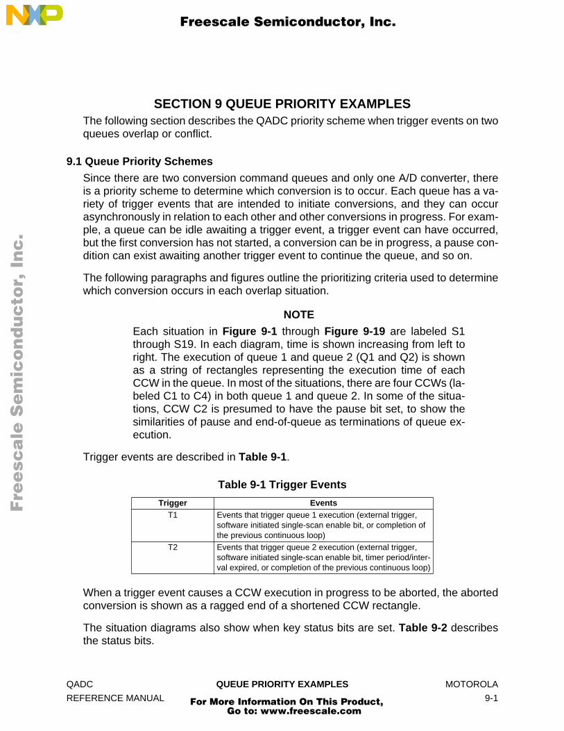
F
ree
sca
le S
em
ico
nd
uc
tor,
I
Freescale Semiconductor, Inc.n
c..
.
SECTION 9 QUEUE PRIORITY EXAMPLESThe following section describes the QADC priority scheme when trigger events on twoqueues overlap or conflict.
9.1 Queue Priority Schemes
Since there are two conversion command queues and only one A/D converter, thereis a priority scheme to determine which conversion is to occur. Each queue has a va-riety of trigger events that are intended to initiate conversions, and they can occurasynchronously in relation to each other and other conversions in progress. For exam-ple, a queue can be idle awaiting a trigger event, a trigger event can have occurred,but the first conversion has not started, a conversion can be in progress, a pause con-dition can exist awaiting another trigger event to continue the queue, and so on.
The following paragraphs and figures outline the prioritizing criteria used to determinewhich conversion occurs in each overlap situation.
NOTE
Each situation in Figure 9-1 through Figure 9-19 are labeled S1through S19. In each diagram, time is shown increasing from left toright. The execution of queue 1 and queue 2 (Q1 and Q2) is shownas a string of rectangles representing the execution time of eachCCW in the queue. In most of the situations, there are four CCWs (la-beled C1 to C4) in both queue 1 and queue 2. In some of the situa-tions, CCW C2 is presumed to have the pause bit set, to show thesimilarities of pause and end-of-queue as terminations of queue ex-ecution.
Trigger events are described in Table 9-1.
When a trigger event causes a CCW execution in progress to be aborted, the abortedconversion is shown as a ragged end of a shortened CCW rectangle.
The situation diagrams also show when key status bits are set. Table 9-2 describesthe status bits.
Table 9-1 Trigger Events
Trigger EventsT1 Events that trigger queue 1 execution (external trigger,
software initiated single-scan enable bit, or completion of the previous continuous loop)
T2 Events that trigger queue 2 execution (external trigger, software initiated single-scan enable bit, timer period/inter-val expired, or completion of the previous continuous loop)
QADC QUEUE PRIORITY EXAMPLES MOTOROLA
REFERENCE MANUAL 9-1
For More Information On This Product, Go to: www.freescale.com

F
ree
sca
le S
em
ico
nd
uc
tor,
I
Freescale Semiconductor, Inc.n
c..
.
Below the queue execution flows are three sets of blocks that show the status infor-mation that is made available to the software. The first two rows of status blocks showthe condition of each queue as:
• Idle• Active• Pause• Suspended• Trigger Pending
The third row of status blocks shows the 4-bit QS status register field that encodes thecondition of the two queues. Two transition status cases, QS = 0011 and QS = 0111,are not shown because they exist only very briefly between stable status conditions.
The first three examples in Figure 9-1, Figure 9-2, and Figure 9-3 (S1, S2, and S3)show what happens when a new trigger event is recognized before the queue hascompleted servicing the previous trigger event on the same queue.
In situation S1 (Figure 9-1), one trigger event is being recognized on each queue whilethat queue is still working on the previously recognized trigger event. The trigger over-run error status bit is set, and otherwise, the premature trigger event is ignored. A trig-ger event which occurs before the servicing of the previous trigger event is through,does not disturb the queue execution in progress.
Figure 9-1 CCW Priority Situation 1
Table 9-2 Status Bits
Bit FunctionCF Flag Set when the end of the queue is reachedPF Flag Set when a queue completes execution up through a
pause bitTrigger Overrun
Error (TOR)Set when a new trigger event occurs before the queue is finished serving the previous trigger event
Q1
Q2
QS
IDLE
IDLE ACTIVE IDLE
0000 1000 0000 0010 0000
TOR1
T1 T1
Q1: C1 C2 C3 C4
CF1
C1 C2 C3 C4
TOR2
T2 T2
Q2:
CF2
IDLE
QADC S1
ACTIVE
MOTOROLA QUEUE PRIORITY EXAMPLES QADC
9-2 REFERENCE MANUAL
For More Information On This Product, Go to: www.freescale.com

F
ree
sca
le S
em
ico
nd
uc
tor,
I
Freescale Semiconductor, Inc.n
c..
.
In situation S2 (Figure 9-2), more than one trigger event is recognized before servicingof a previous trigger event is complete, the trigger overrun bit is again set, but other-wise, the additional trigger events are ignored. After the queue is complete, the firstnewly detected trigger event causes queue execution to begin again. When the triggerevent rate is high, a new trigger event can be seen very soon after completion of theprevious queue, leaving software little time to retrieve the previous results. Also, whentrigger events are occurring at a high rate for queue 1, the lower priority queue 2 chan-nels may not get serviced at all.
Figure 9-2 CCW Priority Situation 2
Figure 9-3 shows that when the pause feature is in use, the trigger overrun error sta-tus bit is set the same way, and that queue execution continues unchanged.
Figure 9-3 CCW Priority Situation 3
QADC S2
ACTIVE IDLEQ1
Q2
QS
IDLE ACTIVE
IDLE ACTIVE IDLE
1000 1000 0000 0010 0000
C1 C2 C3 C4
TOR2
T2 T2
Q2:
CF2
IDLE
C1 C2 C3 C4
T1
CF1
C1 C2 C3 C4
TOR1
T1 T1
Q1:
CF1TOR1
T1
TOR1
T1
TOR2
T2
QADC S3
PAUSE Q1
Q2
QS
IDLE ACTIVE
IDLE ACTIVE IDLE
1000 0110 0001 0010
ACTIVE
0000
IDLE
C1 C2
T1 T1
Q1:
TOR1 PF1
C1 C2
0000
Q2:
0100
TOR2 PF2
T2 T2
0101
C3 C4
T1 T1
TOR1 CF1
ACTIVE
PAUSE
1001
C3 C4
CF2
T2 T2
TOR2
QADC QUEUE PRIORITY EXAMPLES MOTOROLA
REFERENCE MANUAL 9-3
For More Information On This Product, Go to: www.freescale.com

F
ree
sca
le S
em
ico
nd
uc
tor,
I
Freescale Semiconductor, Inc.n
c..
.
The next two situations consider trigger events that occur for the lower priority queue2, while queue 1 is actively being serviced.
Figure 9-4 shows that a queue 2 trigger event that is recognized while queue 1 is ac-tive, is saved, and as soon as queue 1 is finished, queue 2 servicing begins.
Figure 9-4 CCW Priority Situation 4
Situation S5 (Figure 9-5) shows that when multiple queue 2 trigger events are detect-ed while queue 1 is busy, the trigger overrun error bit is set, but queue 1 execution isnot disturbed. Situation S5 also shows that the effect of queue 2 trigger events duringqueue 1 execution is the same when the pause feature is in use in either queue.
Figure 9-5 CCW Priority Situation 5
QADC S4
Q1
Q2
QS
IDLE
IDLE ACTIVE IDLE
0000 1000 0010
ACTIVE
0000
C1 C2 C3 C4
T1
Q1:
CF1
Q2:C1 C2 C3 C4
T2
CF2
IDLE
1011
TRIGGERED
QADC S5
Q1
Q2
QS
IDLE
IDLE IDLE
0000 1000 0010
ACTIVE
0000
C1 C2
T1
Q1:
C1 C2
PF2
C3 C4
C3 C4
CF2
IDLE
1011
TRIG
Q2:
T2T2PF1
PAUSE
ACTIVE PAUSE
TOR1
T2T2CF1
TOR1
T1
ACTIVE
TRIG
0110
ACTIVE
ACTIVE
0101 1001 1011
MOTOROLA QUEUE PRIORITY EXAMPLES QADC
9-4 REFERENCE MANUAL
For More Information On This Product, Go to: www.freescale.com

F
ree
sca
le S
em
ico
nd
uc
tor,
I
Freescale Semiconductor, Inc.n
c..
.
The remaining situations, S6 through S11, show the impact of a queue 1 trigger eventoccurring during queue 2 execution. Queue 1 is higher in priority, the conversion takingplace in queue 2 is aborted, so that there is not a variable latency time in respondingto queue 1 trigger events.
In situation 6 (Figure 9-6), the conversion initiated by the second CCW in queue 2 isaborted just before the conversion is complete, so that queue 1 execution can begin.Queue 2 is considered suspended. After queue 1 is finished, queue 2 starts over withthe first CCW, when the RES (resume) control bit is set to 0. Situation S7 (Figure 9-7) shows that when pause operation is not in use with queue 2, queue 2 suspensionworks the same way.
Figure 9-6 CCW Priority Situation 6
Figure 9-7 CCW Priority Situation 7
QADC S6
IDLE
Q1
Q2
QS
IDLE
IDLE
0000 1000
ACTIVE
C1 C2
T1
Q1:
C1
C3 C4
IDLE
Q2:
PF1
PAUSE
ACTIVE
CF1
T1
ACTIVE
SUSPEND
0100
ACTIVE
ACTIVE
0110 1010
C1 C2 C3 C4
CF2
T2
0010 0000
QADC S7
T1 T1
PAUSE Q1
Q2
QS
IDLE ACTIVE
IDLE IDLE
0010 0110 1010 0010
ACTIVE
0000
IDLE
Q1:
PF1
C1 C2
0000 1010 0101
ACTIVE
PAUSE
0110
C1Q2:
T2
PF2
C1 C2
C3 C4
CF1
C3 C4
CF2
T2
C3
SUSPEND ACTIVE ACT SUSPEND ACTIVE
QADC QUEUE PRIORITY EXAMPLES MOTOROLA
REFERENCE MANUAL 9-5
For More Information On This Product, Go to: www.freescale.com

F
ree
sca
le S
em
ico
nd
uc
tor,
I
Freescale Semiconductor, Inc.n
c..
.
Situations S8 and S9 (Figure 9-8 and Figure 9-9) repeat the same two situations withthe resume bit set to a one. When the RES bit is set, following suspension, queue 2resumes execution with the aborted CCW, not the first CCW in the queue.
Figure 9-8 CCW Priority Situation 8
Figure 9-9 CCW Priority Situation 9
Situations S10 and S11 (Figure 9-10 and Figure 9-11) show that when an additionaltrigger event is detected for queue 2 while the queue is suspended, the trigger overrunerror bit is set, the same as if queue 2 were being executed when a new trigger eventoccurs. Trigger overrun on queue 2 thus permits the software to know that queue 1 istaking up so much QADC time that queue 2 trigger events are being lost.
QADC S8
IDLE
Q1
Q2
QS
IDLE
IDLE
0000 1000 0010
ACTIVE
C1 C2
T1
Q1:
C1
C3 C4
IDLE
Q2:
PF1
PAUSE
ACTIVE
CF1
T1
ACTIVE
SUSPEND
0100
ACTIVE
ACTIVE
0110 1010
C2 C3 C4
CF2
T2
0000
QADC S9
T1
PAUSE Q1
Q2
QS
IDLE ACTIVE
IDLE ACT IDLE
0010 0110 1010 0010
ACTIVE
0000
IDLE
Q1:
PF1
C1 C2
0000 1010 0101
ACTIVE
PAUSE
0110
C1Q2:
T2
C2
PF2
T1
C3 C4
CF1
C4
CF2
SUSPEND ACT ACTIVE SUSPEND
T2
C3C1
MOTOROLA QUEUE PRIORITY EXAMPLES QADC
9-6 REFERENCE MANUAL
For More Information On This Product, Go to: www.freescale.com

F
ree
sca
le S
em
ico
nd
uc
tor,
I
Freescale Semiconductor, Inc.n
c..
.
Figure 9-10 CCW Priority Situation 10
Figure 9-11 CCW Priority Situation 11
The above situations cover normal overlap conditions that arise with asynchronoustrigger events on the two queues. An additional conflict to consider is that the freezecondition can arise while the QADC is actively executing CCWs. The conventional usefor the freeze mode is for software/hardware debugging. When the CPU backgrounddebug mode is enabled and a breakpoint occurs, the freeze signal is issued, which cancause peripheral modules to stop operation. When freeze is detected, the QADC com-pletes the conversion in progress, unlike queue 1 suspending queue 2. After the freezecondition is removed, the QADC continues queue execution with the next CCW in se-quence.
QADC S10
T1 T1
PAUSE Q1
Q2
QS
IDLE ACTIVE
IDLE ACTIVE IDLE
0010 0110 1010 0010
ACTIVE
0000
IDLE
Q1:
PF1
C1 C2
0000 1010 0101
ACTIVE
PAUSE
0110
Q2:
T2
PF2
C1 C2
C3 C4
CF1
C3 C4
CF2
T2
C3
SUSPEND ACTIVE
C1
ACT SUSPEND
T2
TOR2
T2
TOR2
QADC S11
T1 T1
C3 C4
CF1
PAUSE Q1
Q2
QS
IDLE ACTIVE
IDLE ACT IDLE
0010 0110 1010 0010
ACTIVE
0000
IDLE
Q1:
PF1
C1 C2
0000 1010 0101
ACTIVE
PAUSE
0110
Q2:
T2
SUSPEND ACT
C1
ACTIVE SUSPEND
T2
TOR2
T2
TOR2
C2
PF2
C4
CF2
T2
C3
QADC QUEUE PRIORITY EXAMPLES MOTOROLA
REFERENCE MANUAL 9-7
For More Information On This Product, Go to: www.freescale.com
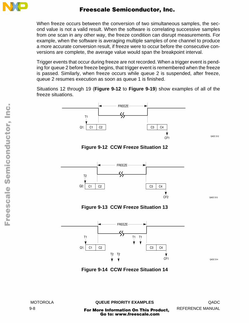
F
ree
sca
le S
em
ico
nd
uc
tor,
I
Freescale Semiconductor, Inc.n
c..
.
When freeze occurs between the conversion of two simultaneous samples, the sec-ond value is not a valid result. When the software is correlating successive samplesfrom one scan in any other way, the freeze condition can disrupt measurements. Forexample, when the software is averaging multiple samples of one channel to producea more accurate conversion result, if freeze were to occur before the consecutive con-versions are complete, the average value would span the breakpoint interval.
Trigger events that occur during freeze are not recorded. When a trigger event is pend-ing for queue 2 before freeze begins, that trigger event is remembered when the freezeis passed. Similarly, when freeze occurs while queue 2 is suspended, after freeze,queue 2 resumes execution as soon as queue 1 is finished.
Situations 12 through 19 (Figure 9-12 to Figure 9-19) show examples of all of thefreeze situations.
Figure 9-12 CCW Freeze Situation 12
Figure 9-13 CCW Freeze Situation 13
Figure 9-14 CCW Freeze Situation 14
QADC S12
C3 C4
CF1
C1 C2
T1
Q1:
FREEZE
QADC S13
C1 C2
T2
Q2:
CF2
C3 C4
FREEZE
QADC S14
C1 C2
T1
Q1:
CF1
C3 C4
FREEZE
T1 T1
T2 T2
MOTOROLA QUEUE PRIORITY EXAMPLES QADC
9-8 REFERENCE MANUAL
For More Information On This Product, Go to: www.freescale.com

F
ree
sca
le S
em
ico
nd
uc
tor,
I
Freescale Semiconductor, Inc.n
c..
.
Figure 9-15 CCW Freeze Situation 15
Figure 9-16 CCW Freeze Situation 16
Figure 9-17 CCW Freeze Situation 17
Figure 9-18 CCW Freeze Situation 18
QADC S15
C1 C2
T2
Q2:
CF2
C3 C4
FREEZE
T2 T2
T1 T1
QADC S16
C1 C2
T1
Q1:
CF1
C3 C4
FREEZE
T1 T1
PF1
QADC S17
C1 C2
T2
Q2:
CF2
C3 C4
FREEZE
T2 T2
PF2
QADC S18
C1 C2
T1
Q1:
CF1
C3 C4
FREEZE
T2
C1 C2Q2: C3
CF2
C4
QADC QUEUE PRIORITY EXAMPLES MOTOROLA
REFERENCE MANUAL 9-9
For More Information On This Product, Go to: www.freescale.com
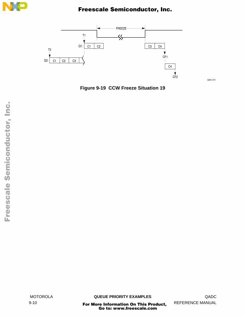
F
ree
sca
le S
em
ico
nd
uc
tor,
I
Freescale Semiconductor, Inc.n
c..
.
Figure 9-19 CCW Freeze Situation 19
QADC S19
C1 C2
T1
Q1:
CF1
C4
FREEZE
CF2
C4
C1 C2
T2
Q2: C3
C3
MOTOROLA QUEUE PRIORITY EXAMPLES QADC
9-10 REFERENCE MANUAL
For More Information On This Product, Go to: www.freescale.com

F
ree
sca
le S
em
ico
nd
uc
tor,
I
Freescale Semiconductor, Inc.n
c..
.
APPENDIX A ELECTRICAL CHARACTERISTICS
NOTES:1. Below disruptive current conditions, the channel being stressed has conversion values of $3FF for analog in-
puts greater than VRH and $000 for values less than VRL. This assumes that VRH ≤ VDDA and VRL ≥ VSSA dueto the presence of the sample amplifier. Other channels are not affected by non-disruptive conditions.
2. Input signals with large slew rates or high frequency noise components cannot be converted accurately. Thesesignals also affect the conversion accuracy of other channels.
3. Exceeding limit may cause conversion error on stressed channels and on unstressed channels. Transitionswithin the limit do not affect device reliability or cause permanent damage.
4. Input must be current limited to the value specified. To determine the value of the required current-limiting re-sistor, calculate resistance values using positive and negative clamp values, then use the larger of the calcu-lated values.
5. This parameter is periodically sampled rather 100% tested.6. Condition applies to one pin at a time.7. Determination of actual maximum disruptive input current, which can affect operation, is related to external sys-
tem component values.8. Current coupling is the ratio of the current induced from overvoltage (positive or negative, through an external
series coupling resistor), divided by the current induced on adjacent pins. A voltage drop may occur across theexternal source impedances of the adjacent pins, impacting conversions on these adjacent pins.
Table A-1 QADC Maximum Ratings
Num Parameter Symbol Min Max Unit1 Analog Supply, with reference to V
SSA VDDA
– 0.3 6.5 V2 Internal Digital Supply, with reference to V
SSI V
DDI– 0.3 6.5 V
3 Reference Supply, with reference to VRL
VRH
– 0.3 6.5 V4 V
SS Differential Voltage VSSI – V
SSA– 0.1 0.1 V
5 VDD Differential Voltage V
DDI – VDDA
– 6.5 6.5 V6 V
REF Differential Voltage VRH
– VRL
– 6.5 6.5 V7 V
RH to V
DDA Differential Voltage VRH – V
DDA– 6.5 6.5 V
8 VRL
to VSSA Differential Voltage V
RL – VSSA
– 6.5 6.5 V9 Disruptive Input Current1, 2, 3, 4, 5, 6, 7
VNEGCLAMP = – 0.3 VVPOSCLAMP = 8 V
INA – 500 500 µA
10 Positive Overvoltage Current Coupling Ratio1, 5, 6, 8
PQAPQB
KP 20002000
— —
11 Negative Overvoltage Current Coupling Ratio1, 5, 6, 8
PQAPQB
KN 125500
— —
12 Maximum Input Current3, 4, 6
VNEGCLAMP = – 0.3 VVPOSCLAMP = 8 V
IMA – 25 25 mA
QADC ELECTRICAL CHARACTERISTICS MOTOROLA
REFERENCE MANUAL A-1
For More Information On This Product, Go to: www.freescale.com
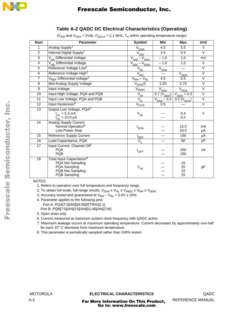
F
ree
sca
le S
em
ico
nd
uc
tor,
I
Freescale Semiconductor, Inc.n
c..
.
NOTES:1. Refers to operation over full temperature and frequency range.2. To obtain full-scale, full-range results, VSSA ≤ VRL ≤ VINDC ≤ VRH ≤ VDDA.3. Accuracy tested and guaranteed at VRH – VRL = 5.0V ± 10%.4. Parameter applies to the following pins:
Port A: PQA[7:0]/AN[59:58]/ETRIG[2:1]Port B: PQB[7:0]/AN[3:0]/AN[51:48]/AN[Z:W]
5. Open drain only.6. Current measured at maximum system clock frequency with QADC active.7. Maximum leakage occurs at maximum operating temperature. Current decreases by approximately one-half
for each 10° C decrease from maximum temperature.8. This parameter is periodically sampled rather than 100% tested.
Table A-2 QADC DC Electrical Characteristics (Operating)(VSSI and VSSA = 0Vdc, FQCLK = 2.1 MHz, TA within operating temperature range)
Num Parameter Symbol Min Max Unit1 Analog Supply1 V
DDA4.5 5.5 V
2 Internal Digital Supply1 VDDI
4.5 5.5 V3 V
SS Differential Voltage VSSI – VSSA
– 1.0 1.0 mV4 V
DD Differential Voltage VDDI – V
DDA– 1.0 1.0 V
5 Reference Voltage Low2 VRL
VSSA
— V6 Reference Voltage High2 V
RH— V
DDA V7 VREF Differential Voltage3 VRH – VRL 4.5 5.5 V8 Mid-Analog Supply Voltage VDDA/2 2.25 2.75 V9 Input Voltage VINDC V
SSAV
DDA V10 Input High Voltage, PQA and PQB V
IH0.7 (V
DDA) V
DDA + 0.3 V11 Input Low Voltage, PQA and PQB V
ILV
SSA – 0.3 0.2 (VDDA
) V12 Input Hysteresis4 VHYS 0.5 — V13 Output Low Voltage, PQA5
IOL
= 5.3 mAIOL
= 10.0 µAV
OL——
0.40.2
V
14 Analog Supply CurrentNormal Operation6
Low-Power StopIDDA
——
15.010.0
mAµA
15 Reference Supply Current IREF
— 150 µA16 Load Capacitance, PQA C
L— 90 pF
17 Input Current, Channel Off7
PQAPQB
IOFF
——
250150
nA
18 Total Input Capacitance8 PQA Not SamplingPQA SamplingPQB Not SamplingPQB Sampling
CIN
————
15201015
pF
MOTOROLA ELECTRICAL CHARACTERISTICS QADC
A-2 REFERENCE MANUAL
For More Information On This Product, Go to: www.freescale.com

F
ree
sca
le S
em
ico
nd
uc
tor,
I
Freescale Semiconductor, Inc.n
c..
.
NOTES:1. Conversion characteristics vary with FQCLK rate. Reduced conversion accuracy occurs at max FQCLK rate.2. Duty cycle must be as close as possible to 75% to achieve optimum performance.3. Minimum applies to 1.0 MHz operation.4. Assumes that short input sample time has been selected (IST = 0).5. Assumes that fSYS = 20.97 MHz.6. Assumes FQCLK = 0.999 MHz, with clock prescaler values of:
QACR0: PSH = %01111, PSA = %1, PSL = 100)CCW: BYP = %0
7. Assumes FQCLK = 2.097 MHz, with clock prescaler values of:QACR0: PSH = %00110, PSA = %1, PSL = 010)CCW: BYP = %0
Table A-3 QADC AC Electrical Characteristics (Operating)(VDDI and VDDA = 5.0 Vdc ± 5%, VSSI and VSSA = 0Vdc, TA within operating temperature range.)
Num Parameter Symbol Min Max Unit1 QADC Clock (QCLK) Frequency1 FQCLK 0.5 2.1 MHz2 QADC Clock Duty Cycle2, 3
High Phase Time (TPSL ≤ TPSH) TPSH 500 — ns3 Conversion Cycles4 CC 18 32 QCLK
cycles4 Conversion Time2,4,5
FQCLK = 0.999 MHz6
Min = CCW/IST = %00Max = CCW/IST = %11
FQCLK = 2.097 MHz1, 7
Min = CCW/IST = %00Max = CCW/IST = %11
TCONV
18.0
8.58
32
15.24µs
5 Stop Mode Recovery Time TSR — 10 µs
QADC ELECTRICAL CHARACTERISTICS MOTOROLA
REFERENCE MANUAL A-3
For More Information On This Product, Go to: www.freescale.com
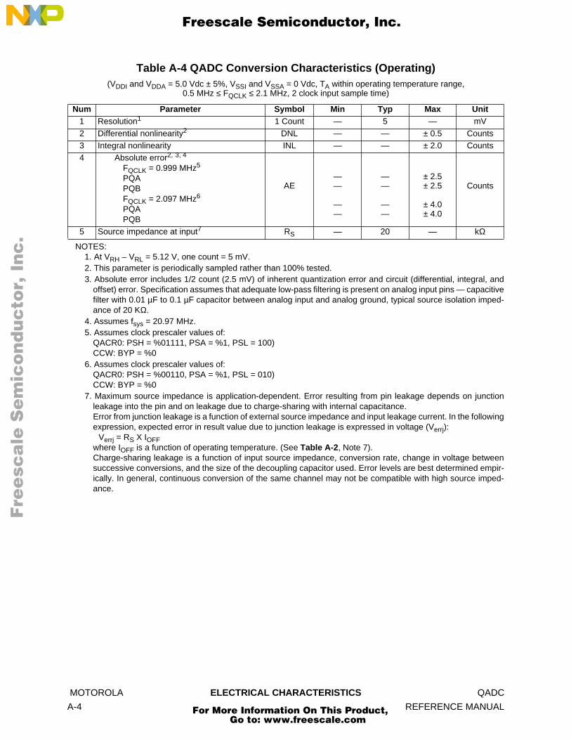
F
ree
sca
le S
em
ico
nd
uc
tor,
I
Freescale Semiconductor, Inc.n
c..
.
NOTES:1. At VRH – VRL = 5.12 V, one count = 5 mV.2. This parameter is periodically sampled rather than 100% tested.3. Absolute error includes 1/2 count (2.5 mV) of inherent quantization error and circuit (differential, integral, and
offset) error. Specification assumes that adequate low-pass filtering is present on analog input pins — capacitivefilter with 0.01 µF to 0.1 µF capacitor between analog input and analog ground, typical source isolation imped-ance of 20 KΩ.
4. Assumes fsys = 20.97 MHz.5. Assumes clock prescaler values of:
QACR0: PSH = %01111, PSA = %1, PSL = 100)CCW: BYP = %0
6. Assumes clock prescaler values of:QACR0: PSH = %00110, PSA = %1, PSL = 010)CCW: BYP = %0
7. Maximum source impedance is application-dependent. Error resulting from pin leakage depends on junctionleakage into the pin and on leakage due to charge-sharing with internal capacitance.Error from junction leakage is a function of external source impedance and input leakage current. In the followingexpression, expected error in result value due to junction leakage is expressed in voltage (Verrj):
Verrj = RS X IOFFwhere IOFF is a function of operating temperature. (See Table A-2, Note 7).Charge-sharing leakage is a function of input source impedance, conversion rate, change in voltage betweensuccessive conversions, and the size of the decoupling capacitor used. Error levels are best determined empir-ically. In general, continuous conversion of the same channel may not be compatible with high source imped-ance.
Table A-4 QADC Conversion Characteristics (Operating)(VDDI and VDDA = 5.0 Vdc ± 5%, VSSI and VSSA = 0 Vdc, TA within operating temperature range,
0.5 MHz ≤ FQCLK ≤ 2.1 MHz, 2 clock input sample time)
Num Parameter Symbol Min Typ Max Unit1 Resolution1 1 Count — 5 — mV2 Differential nonlinearity2 DNL — — ± 0.5 Counts3 Integral nonlinearity INL — — ± 2.0 Counts4 Absolute error2, 3, 4
FQCLK = 0.999 MHz5
PQAPQBFQCLK = 2.097 MHz6
PQAPQB
AE——
——
——
——
± 2.5± 2.5
± 4.0± 4.0
Counts
5 Source impedance at input7 RS — 20 — kΩ
MOTOROLA ELECTRICAL CHARACTERISTICS QADC
A-4 REFERENCE MANUAL
For More Information On This Product, Go to: www.freescale.com
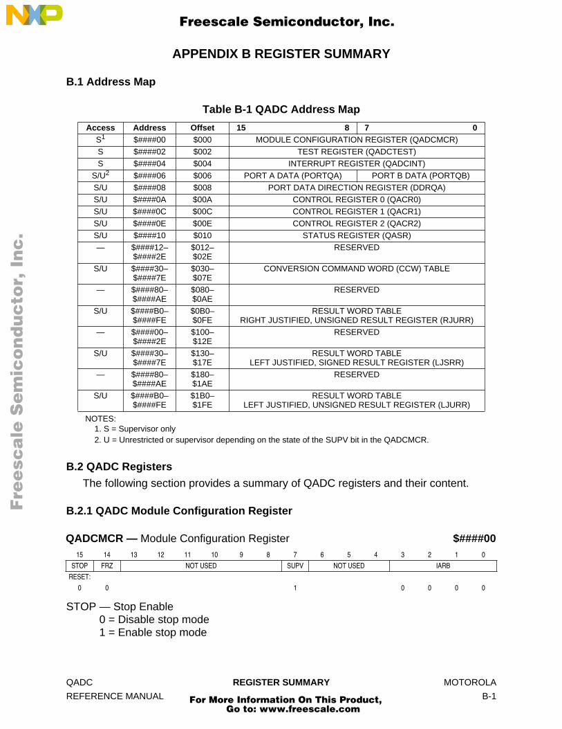
F
ree
sca
le S
em
ico
nd
uc
tor,
I
Freescale Semiconductor, Inc.n
c..
.
APPENDIX B REGISTER SUMMARY
B.1 Address Map
B.2 QADC Registers
The following section provides a summary of QADC registers and their content.
B.2.1 QADC Module Configuration Register
STOP — Stop Enable0 = Disable stop mode1 = Enable stop mode
NOTES:1. S = Supervisor only2. U = Unrestricted or supervisor depending on the state of the SUPV bit in the QADCMCR.
Table B-1 QADC Address Map
Access Address Offset 15 8 7 0S1 $####00 $000 MODULE CONFIGURATION REGISTER (QADCMCR)S $####02 $002 TEST REGISTER (QADCTEST)S $####04 $004 INTERRUPT REGISTER (QADCINT)
S/U2 $####06 $006 PORT A DATA (PORTQA) PORT B DATA (PORTQB)S/U $####08 $008 PORT DATA DIRECTION REGISTER (DDRQA)S/U $####0A $00A CONTROL REGISTER 0 (QACR0)S/U $####0C $00C CONTROL REGISTER 1 (QACR1)S/U $####0E $00E CONTROL REGISTER 2 (QACR2)S/U $####10 $010 STATUS REGISTER (QASR)— $####12–
$####2E$012– $02E
RESERVED
S/U $####30– $####7E
$030– $07E
CONVERSION COMMAND WORD (CCW) TABLE
— $####80– $####AE
$080– $0AE
RESERVED
S/U $####B0– $####FE
$0B0– $0FE
RESULT WORD TABLERIGHT JUSTIFIED, UNSIGNED RESULT REGISTER (RJURR)
— $####00– $####2E
$100– $12E
RESERVED
S/U $####30– $####7E
$130– $17E
RESULT WORD TABLELEFT JUSTIFIED, SIGNED RESULT REGISTER (LJSRR)
— $####80– $####AE
$180– $1AE
RESERVED
S/U $####B0– $####FE
$1B0– $1FE
RESULT WORD TABLELEFT JUSTIFIED, UNSIGNED RESULT REGISTER (LJURR)
QADCMCR — Module Configuration Register $####0015 14 13 12 11 10 9 8 7 6 5 4 3 2 1 0
STOP FRZ NOT USED SUPV NOT USED IARB
RESET:
0 0 1 0 0 0 0
QADC REGISTER SUMMARY MOTOROLA
REFERENCE MANUAL B-1
For More Information On This Product, Go to: www.freescale.com

F
ree
sca
le S
em
ico
nd
uc
tor,
I
Freescale Semiconductor, Inc.n
c..
.
FRZ — Freeze Enable0 = Ignores the IMB IFREEZE signal1 = Finish any current conversion, then freeze
SUPV — Supervisor/Unrestricted Data Space0 = Only the module configuration register, test register, and interrupt register are
designated as supervisor-only data space. Access to all other locations is un-restricted.
1 = All QADC registers and tables are designated as supervisor-only data space.
IARB[3:0] — Software Interrupt Arbitration NumberIARB determines QADC interrupt arbitration priority. The reset value is $F (highest pri-ority), to prevent QADC interrupts from being discarded during initialization.
B.2.2 QADC Test Register
QADCTEST — QADC Test Register $####02
QADCTEST is used only during factory testing of the MCU.
B.2.3 QADC Interrupt Register
IRL1[14:12] — Queue 1 Interrupt LevelThe IRL1 field establishes the queue 1 interrupt request level. The 000 state disablesqueue 1 interrupts by blocking interrupt requests. When queue 1 interrupts are to beused, the IRL1 field must be initialized to a non-zero value. Level 001 is the lowest pri-ority software interrupt request and level 111 is the highest priority request.
IRL2[10:8] — Queue 2 Interrupt LevelThe IRL2 field establishes the queue 2 interrupt request level. The 000 state disablesqueue 2 interrupts by blocking interrupt requests. When queue 2 interrupts are to beused, the IRL2 field must be initialized to a non-zero value. Level 001 is the lowest pri-ority interrupt request and level 111 is the highest priority request.
IVB[7:0] — Interrupt Vector BaseInitialization software inputs the upper six IVB bits in the interrupt register. During in-terrupt arbitration, the vector provided to the CPU by the QADC is made up of the up-per six IVB bits, plus two low-order bits provided to the QADC to identify one of fourQADC interrupt requests. The interrupt vector number is independent of the interruptlevel and the interrupt arbitration number. A $0F vector number corresponds to the un-initialized interrupt vector. After reset, the lower byte of the interrupt register reads as$0F. Once the IVB field is written, the two least significant bits always read as zeros.
NOTES:1. Reserved2. Bits 1 and 0 supplied by the QADC.
QADCINT — QADC Interrupt Register $####0415 14 13 12 11 10 9 8 7 6 5 4 3 2 1 0
—1 IRL1 —1 IRL2 IVB IVB[1:0]2
RESET:
0 0 0 0 0 0 0 0 0 0 1 1
MOTOROLA REGISTER SUMMARY QADC
B-2 REFERENCE MANUAL
For More Information On This Product, Go to: www.freescale.com

F
ree
sca
le S
em
ico
nd
uc
tor,
I
Freescale Semiconductor, Inc.n
c..
.
B.2.4 Port A/B Data Register
QADC ports A and B are accessed through two 8-bit port data registers (PORTQA andPORTQB).
Port A pins are referred to as PQA[7:0] when used as a bidirectional 8-bit input/outputport that may be used for general-purpose digital input signals or digital open drain out-put signals. Port A can also be used for analog inputs (AN[59:52]), external trigger in-puts (ETRIG[2:1]), and external multiplexer address outputs (MA[2:0]).
Port B pins are referred to as PQB[7:0] when used as an input only 8-bit digital portthat may be used for general-purpose digital input signals. Port B can also be used fornonmultiplexed (AN[51:48])/AN[3:0]) and multiplexed (ANz, ANy, ANx, ANw) analoginputs. Read operations on the reserved bits return zeros, and writes have no effect.
B.2.5 Port Data Direction Register
The port data direction register (DDRQA) is associated with the port A digital I/O pins.The bidirectional pins have somewhat higher leakage and capacitance specifications.Refer to APPENDIX A ELECTRICAL CHARACTERISTICS for more information. Anybit in this register set to one configures the corresponding pin as an output. Any bit inthis register cleared to zero configures the corresponding pin as an input. The softwareis responsible for ensuring that DDR bits are not set to one on pins used for analoginputs. When the DDR bit is set to one and the pin is selected for analog conversion,the voltage sampled is that of the output digital driver as influenced by the load.
NOTE
Caution should be exercised when mixing digital and analog inputs.This should be isolated as much as possible. Rise and fall timesshould be as large as possible.
PORTQA — Port A Data Register $####06PORTQB — Port B Data Register $####07
15 14 13 12 11 10 9 8 7 6 5 4 3 2 1 0
PQA7 PQA6 PQA5 PQA4 PQA3 PQA2 PQA1 PQA0 PQB7 PQB6 PQB5 PQB4 PQB3 PQB2 PQB1 PQB0
RESET:
U U U U U U U U U U U U U U U U
ANALOG CHANNEL:
AN59 AN58 AN57 AN56 AN55 AN54 AN53 AN52 AN51 AN50 AN49 AN48 AN3 AN2 AN1 AN0
EXTERNAL TRIGGER INPUTS:
ETRIG2 ETRIG1
MULTIPLEXED ADDRESS OUTPUTS:
MA2 MA1 MA0
MULTIPLEXED ANALOG INPUTS:
ANz ANy ANx ANw
DDRQA — Port Data Direction Register $####0815 14 13 12 11 10 9 8 7 6 5 4 3 2 1 0
DDQA7 DDQA6 DDQA5 DDQA4 DDQA3 DDQA2 DDQA1 DDQA0 RESERVED
RESET:
0 0 0 0 0 0 0 0
QADC REGISTER SUMMARY MOTOROLA
REFERENCE MANUAL B-3
For More Information On This Product, Go to: www.freescale.com

F
ree
sca
le S
em
ico
nd
uc
tor,
I
Freescale Semiconductor, Inc.n
c..
.
Since port B is input-only, a data direction register is not needed. Therefore, the lowerbyte of the port data direction register is not implemented. Read operations on the re-served bits return zeros, and writes have no effect.
B.2.6 QADC Control Registers
MUX — Externally Multiplexed ModeThe MUX bit allows the software to select the externally multiplexed mode, which af-fects the interpretation of the channel numbers and forces the MA0, MA1 and MA2pins to be outputs.
0 = Internally multiplexed, 16 possible channels.1 = Externally multiplexed, 44 possible channels.
PSH[8:4] — Prescaler Clock High TimeThe PSH field selects the QADC clock (QCLK) high time in the prescaler. Table B-2displays the bits in PSH field which enable a range of QCLK high times.
PSA — Prescaler Add a Clock Tic0 = QCLK high and low times are not modified.1 = Add one system clock half cycle to the high time of the QCLK and subtract one
system clock half cycle from the low time.
PSL[2:0] — Prescaler Clock Low TimeThe PSL field selects the QADC clock (QCLK) low time in the prescaler. Table B-2displays the bits in PSL field which enable a range of QCLK low times.
QACR0 — Control Register 0 $####0A15 14 13 12 11 10 9 8 7 6 5 4 3 2 1 0
MUX RESERVED PSH PSA PSL
RESET:
0 0 0 0 1 1 0 0 1 1
Table B-2 Prescaler Clock High Times
PSH[8:4] QCLK High Time PSH[8:4] QCLK High Time00000 1 System Clock Cycle 10000 17 System Clock Cycles00001 2 System Clock Cycles 10001 18 System Clock Cycles00010 3 System Clock Cycles 10010 19 System Clock Cycles00011 4 System Clock Cycles 10011 20 System Clock Cycles00100 5 System Clock Cycles 10100 21 System Clock Cycles00101 6 System Clock Cycles 10101 22 System Clock Cycles00110 7 System Clock Cycles 10110 23 System Clock Cycles00111 8 System Clock Cycles 10111 24 System Clock Cycles01000 9 System Clock Cycles 11000 25 System Clock Cycles01001 10 System Clock Cycles 11001 26 System Clock Cycles01010 11 System Clock Cycles 11010 27 System Clock Cycles01011 12 System Clock Cycles 11011 28 System Clock Cycles01100 13 System Clock Cycles 11100 29 System Clock Cycles01101 14 System Clock Cycles 11101 30 System Clock Cycles01110 15 System Clock Cycles 11110 31 System Clock Cycles01111 16 System Clock Cycles 11111 32 System Clock Cycles
MOTOROLA REGISTER SUMMARY QADC
B-4 REFERENCE MANUAL
For More Information On This Product, Go to: www.freescale.com
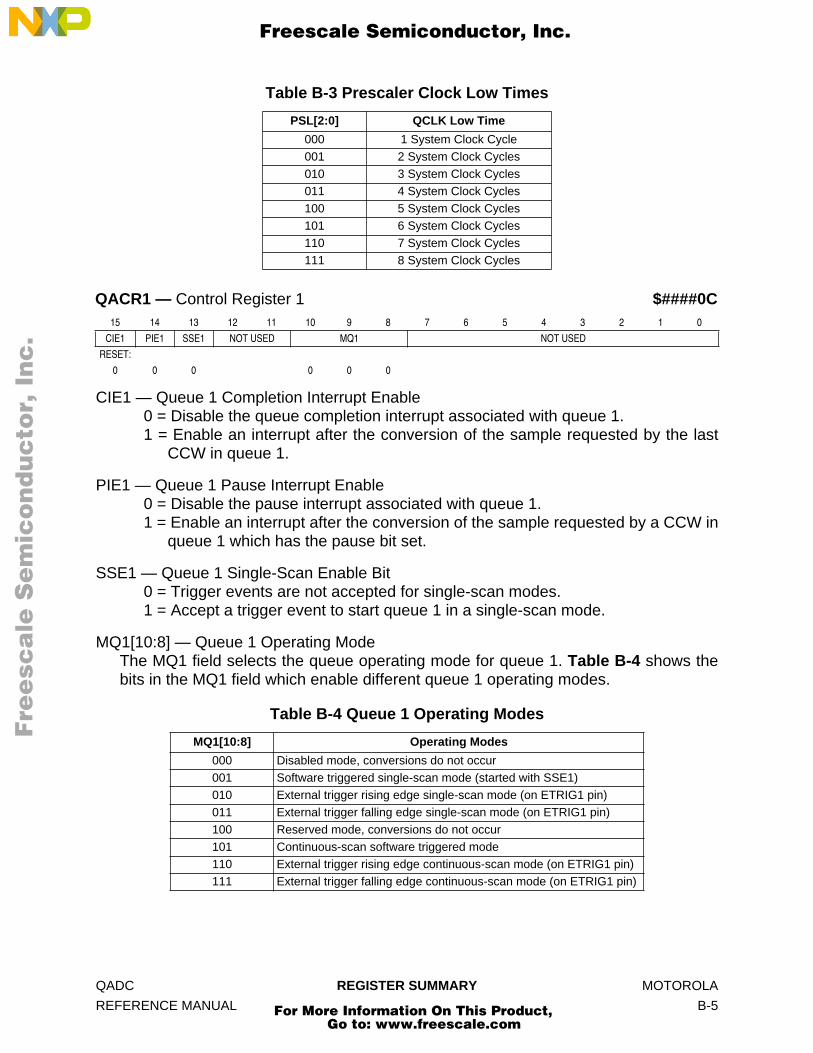
F
ree
sca
le S
em
ico
nd
uc
tor,
I
Freescale Semiconductor, Inc.n
c..
.
CIE1 — Queue 1 Completion Interrupt Enable0 = Disable the queue completion interrupt associated with queue 1.1 = Enable an interrupt after the conversion of the sample requested by the last
CCW in queue 1.
PIE1 — Queue 1 Pause Interrupt Enable0 = Disable the pause interrupt associated with queue 1.1 = Enable an interrupt after the conversion of the sample requested by a CCW in
queue 1 which has the pause bit set.
SSE1 — Queue 1 Single-Scan Enable Bit0 = Trigger events are not accepted for single-scan modes.1 = Accept a trigger event to start queue 1 in a single-scan mode.
MQ1[10:8] — Queue 1 Operating ModeThe MQ1 field selects the queue operating mode for queue 1. Table B-4 shows thebits in the MQ1 field which enable different queue 1 operating modes.
Table B-3 Prescaler Clock Low Times
PSL[2:0] QCLK Low Time
000 1 System Clock Cycle001 2 System Clock Cycles010 3 System Clock Cycles011 4 System Clock Cycles100 5 System Clock Cycles101 6 System Clock Cycles110 7 System Clock Cycles111 8 System Clock Cycles
QACR1 — Control Register 1 $####0C15 14 13 12 11 10 9 8 7 6 5 4 3 2 1 0
CIE1 PIE1 SSE1 NOT USED MQ1 NOT USED
RESET:
0 0 0 0 0 0
Table B-4 Queue 1 Operating Modes
MQ1[10:8] Operating Modes
000 Disabled mode, conversions do not occur001 Software triggered single-scan mode (started with SSE1)010 External trigger rising edge single-scan mode (on ETRIG1 pin)011 External trigger falling edge single-scan mode (on ETRIG1 pin)100 Reserved mode, conversions do not occur101 Continuous-scan software triggered mode110 External trigger rising edge continuous-scan mode (on ETRIG1 pin)111 External trigger falling edge continuous-scan mode (on ETRIG1 pin)
QADC REGISTER SUMMARY MOTOROLA
REFERENCE MANUAL B-5
For More Information On This Product, Go to: www.freescale.com

F
ree
sca
le S
em
ico
nd
uc
tor,
I
Freescale Semiconductor, Inc.n
c..
.
CIE2 — Queue 2 Completion Software Interrupt Enable0 = Disable the queue completion interrupt associated with queue 2.1 = Enable an interrupt after the conversion of the sample requested by the last
CCW in queue 2.
PIE2 — Queue 2 Pause Software Interrupt Enable0 = Disable the pause interrupt associated with queue 2.1 = Enable an interrupt after the conversion of the sample requested by a CCW in
queue 2 which has the pause bit set.
SSE2 — Queue 2 Single-Scan Enable Bit0 = Trigger events are not accepted for single-scan modes.1 = Accept a trigger event to start queue 2 in a single-scan mode.
MQ2[12:8] — Queue 2 Operating ModeThe MQ2 field selects the queue operating mode for queue 2. Table B-5 shows thebits in the MQ2 field which enable different queue 2 operating modes.
QACR2 — Control Register 2 $####0E15 14 13 12 11 10 9 8 7 6 5 4 3 2 1 0
CIE2 PIE2 SSE2 MQ2 RES NOT USED
BQ2
RESET:
0 0 0 0 0 0 0 0 0 1 0 0 1 1 1
Table B-5 Queue 2 Operating Modes
MQ2[12:8] Operating Modes
00000 Disabled mode, conversions do not occur00001 Software triggered single-scan mode (started with SSE2)00010 External trigger rising edge single-scan mode (on ETRIG2 pin)00011 External trigger falling edge single-scan mode (on ETRIG2 pin)00100 Interval timer single-scan mode: time = QCLK period x 27
00101 Interval timer single-scan mode: time = QCLK period x 28
00110 Interval timer single-scan mode: time = QCLK period x 29
00111 Interval timer single-scan mode: time = QCLK period x 210
01000 Interval timer single-scan mode: time = QCLK period x 211
01001 Interval timer single-scan mode: time = QCLK period x 212
01010 Interval timer single-scan mode: time = QCLK period x 213
01011 Interval timer single-scan mode: time = QCLK period x 214
01100 Interval timer single-scan mode: time = QCLK period x 215
01101 Interval timer single-scan mode: time = QCLK period x 216
01110 Interval timer single-scan mode: time = QCLK period x 217
01111 Reserved mode10000 Reserved mode10001 Continuous-scan software triggered mode10010 External trigger rising edge continuous-scan mode (on ETRIG2 pin)10011 External trigger falling edge continuous-scan mode (on ETRIG2 pin)10100 Periodic timer continuous-scan mode: time = QCLK period x 27
10101 Periodic timer continuous-scan mode: time = QCLK period x 28
10110 Periodic timer continuous-scan mode: time = QCLK period x 29
MOTOROLA REGISTER SUMMARY QADC
B-6 REFERENCE MANUAL
For More Information On This Product, Go to: www.freescale.com
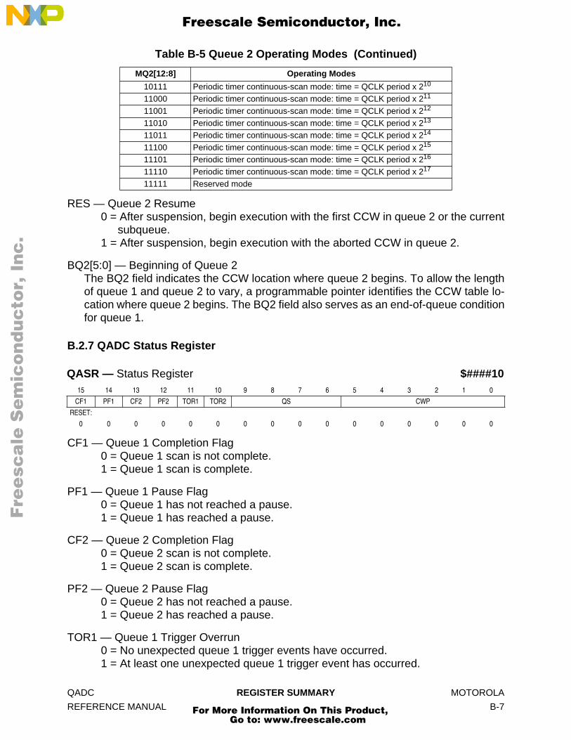
F
ree
sca
le S
em
ico
nd
uc
tor,
I
Freescale Semiconductor, Inc.n
c..
.
RES — Queue 2 Resume0 = After suspension, begin execution with the first CCW in queue 2 or the current
subqueue.1 = After suspension, begin execution with the aborted CCW in queue 2.
BQ2[5:0] — Beginning of Queue 2The BQ2 field indicates the CCW location where queue 2 begins. To allow the lengthof queue 1 and queue 2 to vary, a programmable pointer identifies the CCW table lo-cation where queue 2 begins. The BQ2 field also serves as an end-of-queue conditionfor queue 1.
B.2.7 QADC Status Register
CF1 — Queue 1 Completion Flag0 = Queue 1 scan is not complete.1 = Queue 1 scan is complete.
PF1 — Queue 1 Pause Flag0 = Queue 1 has not reached a pause.1 = Queue 1 has reached a pause.
CF2 — Queue 2 Completion Flag0 = Queue 2 scan is not complete.1 = Queue 2 scan is complete.
PF2 — Queue 2 Pause Flag0 = Queue 2 has not reached a pause.1 = Queue 2 has reached a pause.
TOR1 — Queue 1 Trigger Overrun0 = No unexpected queue 1 trigger events have occurred.1 = At least one unexpected queue 1 trigger event has occurred.
10111 Periodic timer continuous-scan mode: time = QCLK period x 210
11000 Periodic timer continuous-scan mode: time = QCLK period x 211
11001 Periodic timer continuous-scan mode: time = QCLK period x 212
11010 Periodic timer continuous-scan mode: time = QCLK period x 213
11011 Periodic timer continuous-scan mode: time = QCLK period x 214
11100 Periodic timer continuous-scan mode: time = QCLK period x 215
11101 Periodic timer continuous-scan mode: time = QCLK period x 216
11110 Periodic timer continuous-scan mode: time = QCLK period x 217
11111 Reserved mode
QASR — Status Register $####1015 14 13 12 11 10 9 8 7 6 5 4 3 2 1 0
CF1 PF1 CF2 PF2 TOR1 TOR2 QS CWP
RESET:
0 0 0 0 0 0 0 0 0 0 0 0 0 0 0 0
Table B-5 Queue 2 Operating Modes (Continued)
MQ2[12:8] Operating Modes
QADC REGISTER SUMMARY MOTOROLA
REFERENCE MANUAL B-7
For More Information On This Product, Go to: www.freescale.com

F
ree
sca
le S
em
ico
nd
uc
tor,
I
Freescale Semiconductor, Inc.n
c..
.
TOR2 — Queue 2 Trigger Overrun0 = No unexpected queue 2 trigger events have occurred.1 = At least one unexpected queue 2 trigger event has occurred.
QS[9:6] — Queue StatusTable B-6 shows the bits in the QS field and how they affect the status of queue 1 andqueue 2.
CWP — Command Word PointerThe CWP allows the software to know which CCW is executing at present, or was lastcompleted. The command word pointer is a software read-only field, and write opera-tions have no effect.
B.2.8 Conversion Command Word Table
P — Pause0 = Do not enter the pause state after execution of the current CCW.1 = Enter the pause state after execution of the current CCW.
BYP — Sample Amplifier Bypass0 = Amplifier bypass mode disabled.1 = Amplifier bypass mode enabled.
Table B-6 Queue Status
QS[9:6] Queue 1/Queue 2 States
0000 Queue 1 idle, Queue 2 idle0001 Queue 1 idle, Queue 2 paused0010 Queue 1 idle, Queue 2 active0011 Queue 1 idle, Queue 2 trigger pending0100 Queue 1 paused, Queue 2 idle0101 Queue 1 paused, Queue 2 paused0110 Queue 1 paused, Queue 2 active0111 Queue 1 paused, Queue 2 trigger pending1000 Queue 1 active, Queue 2 idle1001 Queue 1 active, Queue 2 paused1010 Queue 1 active, Queue 2 suspended1011 Queue 1 active, Queue 2 trigger pending1100 Reserved1101 Reserved1110 Reserved1111 Reserved
CCW — Conversion Command Word Table $####30–$####7E15 14 13 12 11 10 9 8 7 6 5 4 3 2 1 0
NOT USED P BYP IST CHAN
RESET:
U U U U U U U U U U
MOTOROLA REGISTER SUMMARY QADC
B-8 REFERENCE MANUAL
For More Information On This Product, Go to: www.freescale.com

F
ree
sca
le S
em
ico
nd
uc
tor,
I
Freescale Semiconductor, Inc.n
c..
.
IST[7:6] — Input Sample TimeThe IST field allows software to specify the length of the sample window. Table B-7shows the bits in the IST field which enable different input sample times.
CHAN[5:0] — Channel NumberThe CHAN field selects the input channel number. Table B-8 shows the channel num-ber assignments for the nonmultiplexed mode. Table B-9 shows the channel numberassignments for the multiplexed mode.
Table B-7 Input Sample Times
IST[7:6] Input Sample Times00 Input sample time = QCLK period x 201 Input sample time = QCLK period x 410 Input sample time = QCLK period x 811 Input sample time = QCLK period x 16
QADC REGISTER SUMMARY MOTOROLA
REFERENCE MANUAL B-9
For More Information On This Product, Go to: www.freescale.com
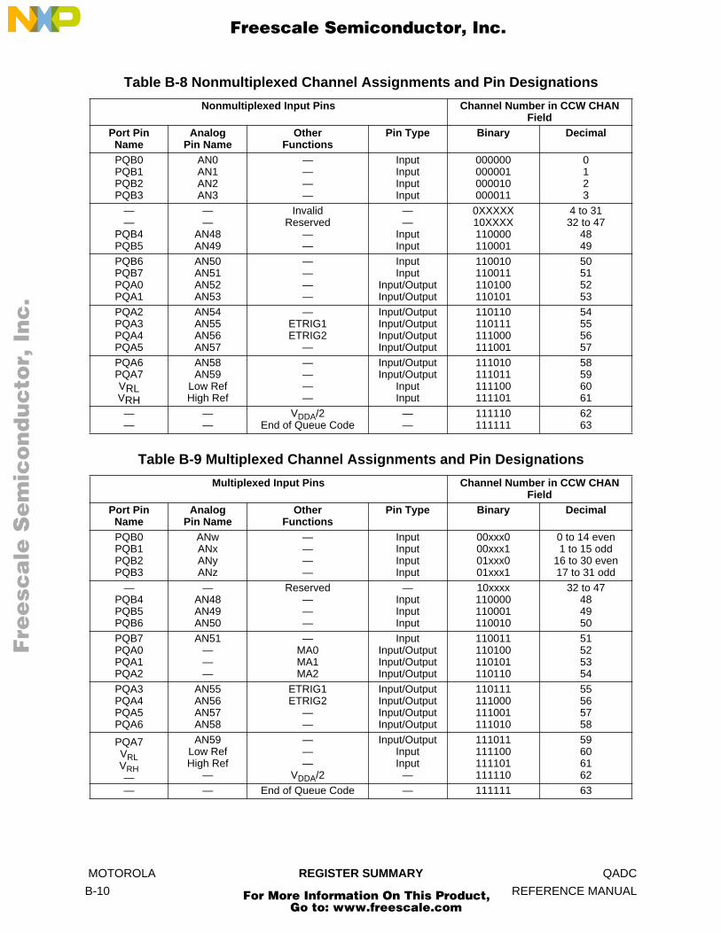
F
ree
sca
le S
em
ico
nd
uc
tor,
I
Freescale Semiconductor, Inc.n
c..
.
Table B-8 Nonmultiplexed Channel Assignments and Pin Designations
Nonmultiplexed Input Pins Channel Number in CCW CHAN Field
Port Pin Name
Analog Pin Name
Other Functions
Pin Type Binary Decimal
PQB0PQB1PQB2PQB3
AN0AN1AN2AN3
————
InputInputInputInput
000000000001000010000011
0123
——
PQB4PQB5
——
AN48AN49
InvalidReserved
——
——
InputInput
0XXXXX10XXXX110000110001
4 to 3132 to 47
4849
PQB6PQB7PQA0PQA1
AN50AN51AN52AN53
————
InputInput
Input/OutputInput/Output
110010110011110100110101
50515253
PQA2PQA3PQA4PQA5
AN54AN55AN56AN57
—ETRIG1ETRIG2
—
Input/OutputInput/OutputInput/OutputInput/Output
110110110111111000111001
54555657
PQA6PQA7VRLVRH
AN58AN59
Low RefHigh Ref
————
Input/OutputInput/Output
InputInput
111010111011111100111101
58596061
——
——
VDDA/2End of Queue Code
——
111110111111
6263
Table B-9 Multiplexed Channel Assignments and Pin Designations
Multiplexed Input Pins Channel Number in CCW CHAN Field
Port Pin Name
Analog Pin Name
Other Functions
Pin Type Binary Decimal
PQB0PQB1PQB2PQB3
ANwANxANyANz
————
InputInputInputInput
00xxx000xxx101xxx001xxx1
0 to 14 even1 to 15 odd
16 to 30 even17 to 31 odd
—PQB4PQB5PQB6
—AN48AN49AN50
Reserved———
—InputInputInput
10xxxx110000110001110010
32 to 47484950
PQB7PQA0PQA1PQA2
AN51———
—MA0MA1MA2
InputInput/OutputInput/OutputInput/Output
110011110100110101110110
51525354
PQA3PQA4PQA5PQA6
AN55AN56AN57AN58
ETRIG1ETRIG2
——
Input/OutputInput/OutputInput/OutputInput/Output
110111111000111001111010
55565758
PQA7VRLVRH—
AN59Low RefHigh Ref
—
———
VDDA/2
Input/OutputInputInput
—
111011111100111101111110
59606162
— — End of Queue Code — 111111 63
MOTOROLA REGISTER SUMMARY QADC
B-10 REFERENCE MANUAL
For More Information On This Product, Go to: www.freescale.com
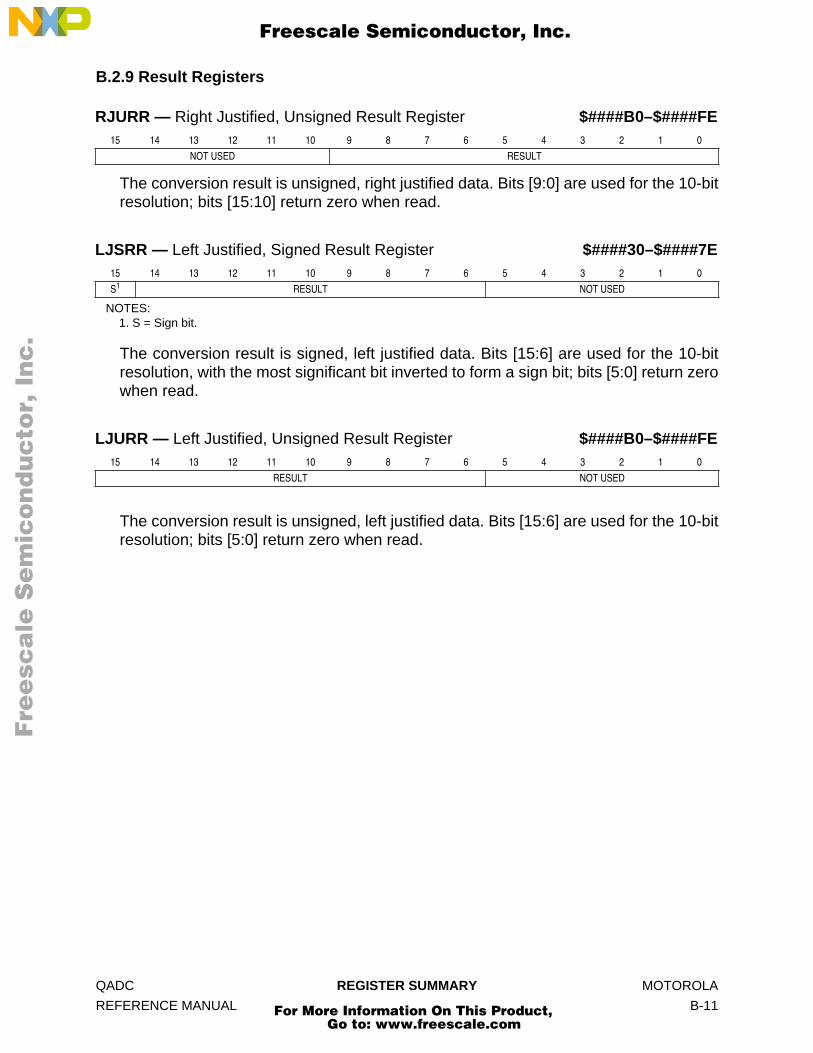
F
ree
sca
le S
em
ico
nd
uc
tor,
I
Freescale Semiconductor, Inc.n
c..
.
B.2.9 Result Registers
The conversion result is unsigned, right justified data. Bits [9:0] are used for the 10-bitresolution; bits [15:10] return zero when read.
The conversion result is signed, left justified data. Bits [15:6] are used for the 10-bitresolution, with the most significant bit inverted to form a sign bit; bits [5:0] return zerowhen read.
The conversion result is unsigned, left justified data. Bits [15:6] are used for the 10-bitresolution; bits [5:0] return zero when read.
NOTES:1. S = Sign bit.
RJURR — Right Justified, Unsigned Result Register $####B0–$####FE15 14 13 12 11 10 9 8 7 6 5 4 3 2 1 0
NOT USED RESULT
LJSRR — Left Justified, Signed Result Register $####30–$####7E15 14 13 12 11 10 9 8 7 6 5 4 3 2 1 0
S1 RESULT NOT USED
LJURR — Left Justified, Unsigned Result Register $####B0–$####FE15 14 13 12 11 10 9 8 7 6 5 4 3 2 1 0
RESULT NOT USED
QADC REGISTER SUMMARY MOTOROLA
REFERENCE MANUAL B-11
For More Information On This Product, Go to: www.freescale.com

F
ree
sca
le S
em
ico
nd
uc
tor,
I
Freescale Semiconductor, Inc.n
c..
.
MOTOROLA REGISTER SUMMARY QADC
B-12 REFERENCE MANUAL
For More Information On This Product, Go to: www.freescale.com

F
ree
sca
le S
em
ico
nd
uc
tor,
I
Freescale Semiconductor, Inc.n
c..
.
APPENDIX C CONVERSION ACCURACY DEFINITIONSThis section explains the terminology used to specify the analog characteristics of theQADC.
C.1 Transfer Curve
Figure C-1 is a plot of the conversion result versus the absolute input voltage. The ide-al curve can be thought of as a staircase of uniform step size with perfect positioningof the endpoints (without gain or offset errors).
Figure C-1 Transfer Curve of an Ideal 10-Bit A/D Converter
The ideal transfer curve has the midpoint code of $000 at the origin, so that the tran-sition of the conversion result from $000 to $001 occurs for an input of one half LSB.Since the input range spans the 1024 codes from $000 to $3FF, the full scale result of$3FF is centered at one least significant (LSB) below the full scale input for an idealconverter.
For example, a 10-bit converter with a reference voltage of 5.12 V (a binary multiple)has an LSB of exactly 5 mV; there are 1024 values from $000 to $3FF. For an idealconverter, the first transition (from $000 to $001) occurs at 2.5 mV, and the last tran-sition (from $3FE to $3FF) occurs at 5.1125 V, or one and one half LSBs before fullscale.
QADC 10-BIT IDEAL
0
INPUT VOLTAGE (LSBs)
1-BIT ACCURACY
CO
NVE
RSI
ON
RES
ULT
$000
$001
$002
$003
$004
$005
$3FB
$3FC
$3FD
$3FE
$3FF
OFFSET
QUANTIZATION ERROR OFFSET
1 2 3 4 5 FS–3 FS–4 FS–3 FS–2 FS–1 FS
QADC CONVERSION ACCURACY DEFINITIONS MOTOROLA
REFERENCE MANUAL C-1
For More Information On This Product, Go to: www.freescale.com
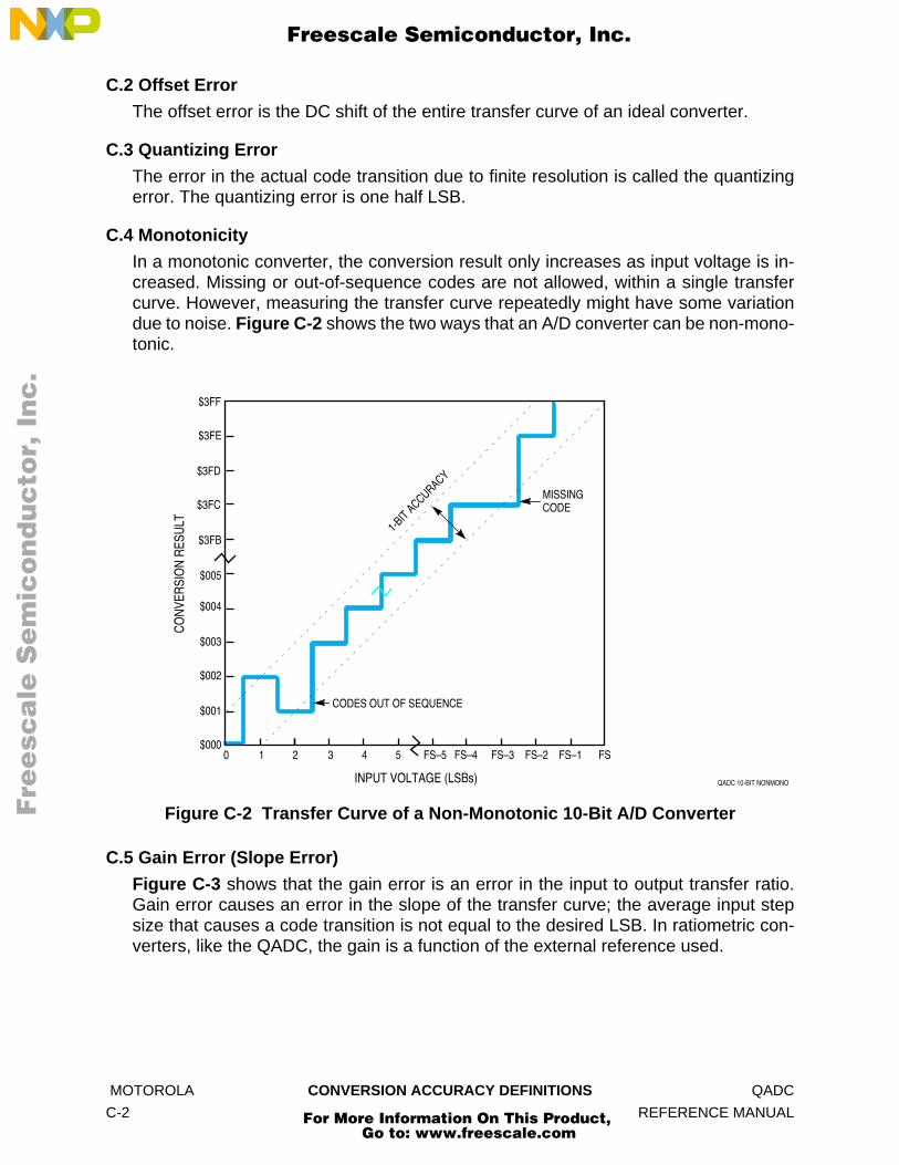
F
ree
sca
le S
em
ico
nd
uc
tor,
I
Freescale Semiconductor, Inc.n
c..
.
C.2 Offset Error
The offset error is the DC shift of the entire transfer curve of an ideal converter.
C.3 Quantizing Error
The error in the actual code transition due to finite resolution is called the quantizingerror. The quantizing error is one half LSB.
C.4 Monotonicity
In a monotonic converter, the conversion result only increases as input voltage is in-creased. Missing or out-of-sequence codes are not allowed, within a single transfercurve. However, measuring the transfer curve repeatedly might have some variationdue to noise. Figure C-2 shows the two ways that an A/D converter can be non-mono-tonic.
Figure C-2 Transfer Curve of a Non-Monotonic 10-Bit A/D Converter
C.5 Gain Error (Slope Error)
Figure C-3 shows that the gain error is an error in the input to output transfer ratio.Gain error causes an error in the slope of the transfer curve; the average input stepsize that causes a code transition is not equal to the desired LSB. In ratiometric con-verters, like the QADC, the gain is a function of the external reference used.
QADC 10-BIT NONMONO
CODES OUT OF SEQUENCE
0
1-BIT ACCURACY
$000
$001
$002
$003
$004
$005
$3FB
$3FC
$3FD
$3FE
$3FF
1 2 3 4 5 FS–5 FS–4 FS–3 FS–2 FS–1 FS
MISSINGCODE
INPUT VOLTAGE (LSBs)
CO
NVE
RSI
ON
RES
ULT
MOTOROLA CONVERSION ACCURACY DEFINITIONS QADC
C-2 REFERENCE MANUAL
For More Information On This Product, Go to: www.freescale.com
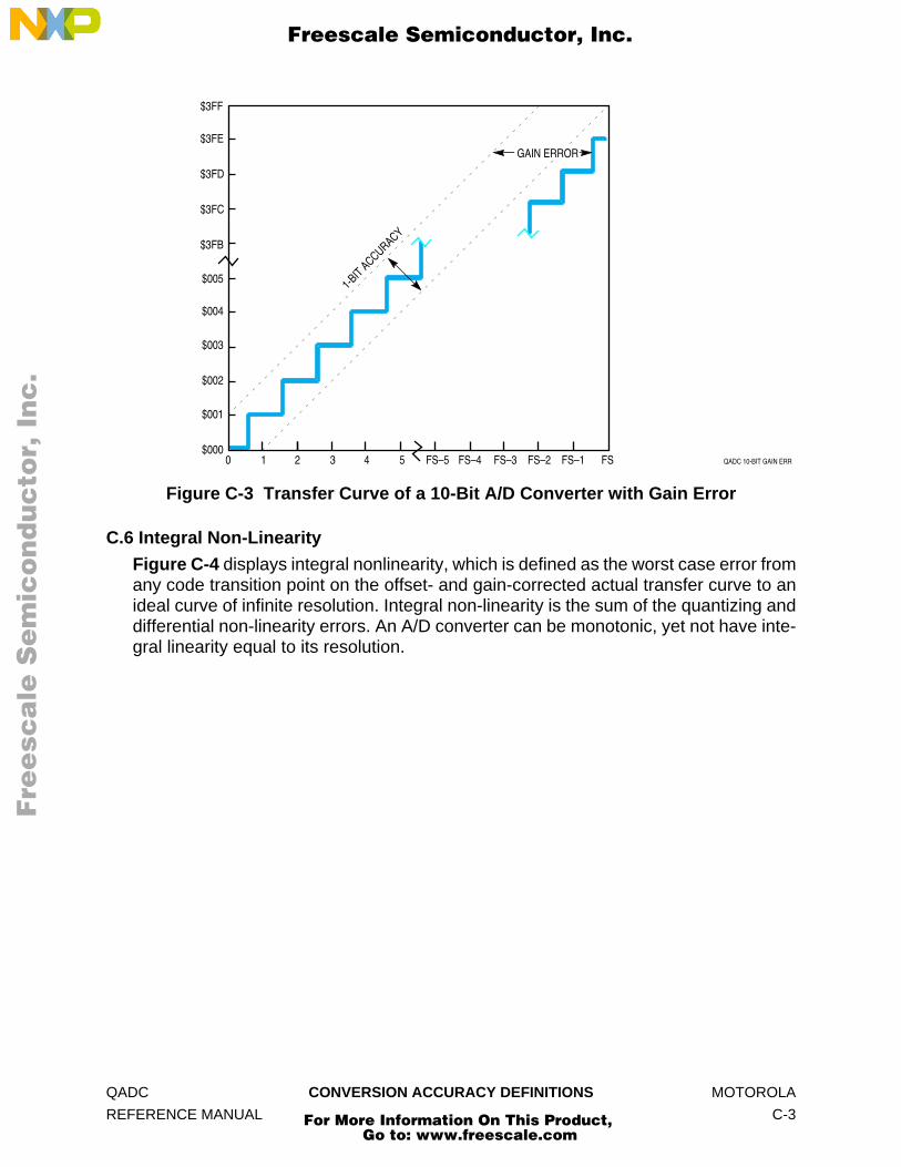
F
ree
sca
le S
em
ico
nd
uc
tor,
I
Freescale Semiconductor, Inc.n
c..
.
Figure C-3 Transfer Curve of a 10-Bit A/D Converter with Gain Error
C.6 Integral Non-Linearity
Figure C-4 displays integral nonlinearity, which is defined as the worst case error fromany code transition point on the offset- and gain-corrected actual transfer curve to anideal curve of infinite resolution. Integral non-linearity is the sum of the quantizing anddifferential non-linearity errors. An A/D converter can be monotonic, yet not have inte-gral linearity equal to its resolution.
QADC 10-BIT GAIN ERR0
1-BIT ACCURACY
$000
$001
$002
$003
$004
$005
$3FB
$3FC
$3FD
$3FE
$3FF
1 2 3 4 5 FS–5 FS–4 FS–3 FS–2 FS–1 FS
GAIN ERROR
QADC CONVERSION ACCURACY DEFINITIONS MOTOROLA
REFERENCE MANUAL C-3
For More Information On This Product, Go to: www.freescale.com

F
ree
sca
le S
em
ico
nd
uc
tor,
I
Freescale Semiconductor, Inc.n
c..
.
Figure C-4 Transfer Curve of a 10-Bit A/D Converter With Integral > One LSB
C.7 Differential Non-Linearity (Related to Monotonicity)
Figure C-5 displays differential nonlinearity, which is defined as the input step size be-tween any two adjacent code transitions. To guarantee monotonicity, the input voltagestep size must range between zero and two LSBs, not including the endpoints(0<Step<2). For monotonicity, the magnitude of the differential linearity error must beless than one LSB. A monotonic A/D converter could have offset or step errors causingall or part of the curve to fall outside the limits of integral accuracy, as long as all inputstep sizes fall between zero and two LSBs.
QADC 10-BIT INTEGRAL ERR
INTEGRAL ERROR
0
1-BIT ACCURACY
$000
$3FF
FS
INPUT VOLTAGE (LSBs)
CO
NVE
RSI
ON
RES
ULT
INTEGRAL ERROR
MOTOROLA CONVERSION ACCURACY DEFINITIONS QADC
C-4 REFERENCE MANUAL
For More Information On This Product, Go to: www.freescale.com
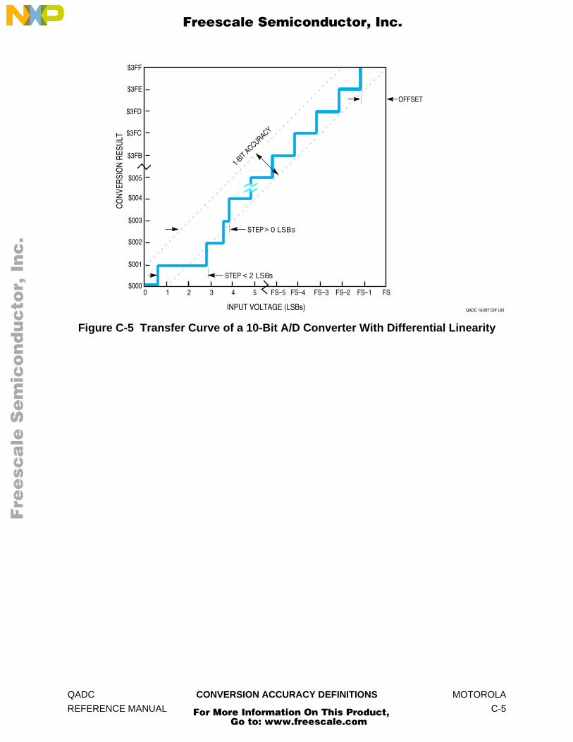
F
ree
sca
le S
em
ico
nd
uc
tor,
I
Freescale Semiconductor, Inc.n
c..
.
Figure C-5 Transfer Curve of a 10-Bit A/D Converter With Differential Linearity
QADC 10-BIT DIF LIN
STEP > 0 LSBs
STEP < 2 LSBs
0
1-BIT ACCURACY
$000
$001
$002
$003
$004
$005
$3FB
$3FC
$3FD
$3FE
$3FF
1 2 3 4 5 FS–5 FS–4 FS–3 FS–2 FS–1 FS
OFFSET
INPUT VOLTAGE (LSBs)
CO
NVE
RSI
ON
RES
ULT
QADC CONVERSION ACCURACY DEFINITIONS MOTOROLA
REFERENCE MANUAL C-5
For More Information On This Product, Go to: www.freescale.com

F
ree
sca
le S
em
ico
nd
uc
tor,
I
Freescale Semiconductor, Inc.n
c..
.
MOTOROLA CONVERSION ACCURACY DEFINITIONS QADC
C-6 REFERENCE MANUAL
For More Information On This Product, Go to: www.freescale.com

INDEX
F
ree
sca
le S
em
ico
nd
uc
tor,
I
Freescale Semiconductor, Inc.n
c..
.
–A–
Accessesbyte 3-2clock requirements 3-1long word 3-1, 3-3misaligned 3-1word 3-2
Address space 3-4AN 2-2, 2-3Analog
front-end multiplexer 6-3input
considerations 5-6multiplexed 2-3pins 5-8port A 2-2port B 2-2
power pins 5-1reference pins 5-1section contents 1-1submodule block diagram 6-1supply
filtering and grounding 5-3pins 2-4
to digital converter operation 6-1
–B–
Beginning of queue 2 (BQ2) 7-19, B-7Binary
divider 7-10-weighted capacitors 6-3
BIU 1-2, 3-1Boundary conditions 7-3BQ2 7-3, 7-19, B-7Bus interface unit (BIU) 1-2
components 3-1BYP 6-2, 7-30, B-8Bypass mode 6-2
–C–
CCW 1-1, 7-26, B-8CF 5-9CF1 7-21, B-7CF2 7-22, B-7CHAN 7-31, B-9Channel
assignments (multiplexed) 7-32, B-10
assignments (nonmultiplexed) 7-31, B-10invalid 7-32number (CHAN) 7-31, B-9reserved 7-32
Charge sharing 5-10CIE1 7-16, B-5CIE2 7-17, B-6Clock
block diagram 7-10frequency 7-11generation 7-9requirements 3-1
Coherency 3-1, 7-8, 7-19Command word pointer (CWP) 7-26, B-8Comparator 6-4Control registers
0 (QACR0) 1-4, 7-14, B-41 (QACR1) 1-4, 7-16, B-52 (QACR2) 1-4, 7-17, B-6
Conversioncommand word table (CCW) 1-1, 7-1, 7-26, B-8cycle times 6-2stages 7-28
CPU16 8-3
condition code register 8-5reference 8-5
32 8-3reference 8-5status register 8-5
misaligned accesses 3-1supervisor/user access 1-3wait states 3-1
CWP 7-26, B-8
–D–
DAC 1-1DDRQA 3-7, B-3Differential non-linearity C-4Digital
control sectioncontents 1-1, 7-1–7-33
input port (PQB) 2-2input/output port (PQA) 2-2to analog converter (DAC) 1-1, 6-3
Disabled mode 7-4
QADC INDEX MOTOROLA
REFERENCE MANUAL I-1
For More Information On This Product, Go to: www.freescale.com

F
ree
sca
le S
em
ico
nd
uc
tor,
I
Freescale Semiconductor, Inc.n
c..
.
–E–
End-of-queue condition 7-28EOQ 7-3Error
gain/slope C-2offset C-2quantizing C-2resulting from leakage 5-10
ETRIG 2-3Exception vector table 8-5External
digital supply pin 2-4leakage 5-10multiplexing 4-1–??trigger continuous-scan mode 7-9trigger pins 2-3trigger single-scan mode 7-6
Externally multiplexed mode (MUX) 7-14, B-4
–F–
FC 3-4Final sample time 6-2FQCLK 7-10, 7-14Freeze
enable (FRZ) 3-5, B-2mode 3-4
FREEZE (internal signal) 3-4, 7-29, B-2FRZ 3-4, 3-5, B-2FSYS 7-12Function code 3-4
–G–
Gain error C-2Global registers 1-4
–I–
I/O port operation 3-6IARB 3-5, 3-6, 8-4, B-2IMB 1-1, 7-9Initial sample time 6-2Input
sample time (IST) 7-12, 7-30, B-9Integral non-linearity C-3Intermodule bus (IMB) 1-1, 3-1Internal digital supply pins 2-4Interrupt
arbitration 8-4arbitration number (IARB) 3-5, B-2arbitration priority 3-5, B-2initializing 8-5polled vs interrupt operation 8-1priority 8-3priority mask 8-3processing summary 8-6recognition and servicing 8-1–8-6
register (QADCINT) 1-4, 8-2, B-2sources 8-2vector base (IVB) 8-3, B-2vectors 8-4
Interval timer single-scan mode 7-6Invalid channel number 7-32IRL1 8-3, B-2IRL2 8-3, B-2IST 7-12, 7-30, B-9IVB 8-3, 8-4, B-2
–L–
Least significant bit (LSB) 6-3Left justified
signed result word table (LJSRR) 7-33, B-11unsigned result word table (LJURR) 7-33, B-11
LJSRR 7-33, B-11LJURR 7-33, B-11LSB 6-3
–M–
MA 3-6Memory map B-1Mid-analog supply voltage 6-3Modes
disabled 7-4freeze 3-4reserved 7-4scan. See Scan modesstop 3-3
Module configuration register (QADCMCR) 1-4, 3-3, B-1Monotonic converter. See monotonicityMonotonicity C-2Most significant bit (MSB) 6-3MQ1 7-17, B-5MQ2 7-18, B-6MSB 6-3Multiple end-of-queue 7-3Multiplexed
analog inputs 2-3MUX 3-6, 7-14, B-4
–N–
Negative stress 5-5Non-linearity
differential C-4integral C-3
–O–
Offset error C-2Open drain drivers 2-2
MOTOROLA INDEX QADC
I-2 REFERENCE MANUAL
For More Information On This Product, Go to: www.freescale.com

F
ree
sca
le S
em
ico
nd
uc
tor,
I
Freescale Semiconductor, Inc.n
c..
.
–P–
P 7-29, B-8Pause (P) 7-1, 7-29, B-8Periodic/interval timer 7-13
continuous-scan mode 7-9PF1 7-21, B-7PF2 7-22, B-7PIE1 7-16, B-5PIE2 7-18, B-6Port
A data register (PORTQA) 3-6, B-3B data register (PORTQB) 3-6, B-3data direction register (DDRQA) 3-7, B-3
PORTQA 3-6, B-3PORTQB 3-6, B-3Positive stress 5-5PQA 2-2, 3-7PQB 2-2, 3-7Prescaler 7-11
add a clock tic (PSA) 7-11, 7-15, B-4clock high time (PSH) 7-11, 7-14, B-4clock low time (PSL) 7-11, 7-16, B-4QACR0 field values 7-11
PSA 7-11, 7-13, 7-15, B-4PSH 7-11, 7-14, B-4PSL 7-11, 7-16, B-4
–Q–
QACR0 1-4, 7-14, B-4QACR1 1-4, 7-16, B-5QACR2 1-4, 7-17, B-6QADC
block diagram 1-1clock (QCLK) 6-2conversion characteristics (operating) A-4electrical characteristics (operating)
AC A-3DC A-2
features 1-2maximum ratings A-1memory map 1-2, B-1pin functions diagram 2-1
QADCINT 1-4, 8-2, B-2QADCMCR 1-4, 3-3, 3-5, B-1QADCTEST 1-4, 3-6, B-2QASR 1-4, 7-20, B-7QCLK 6-2, 7-9
frequency 7-10high time 7-13low time 7-13
QS 7-24, B-8Quantizing error C-2Queue 7-1
1 completion flag (CF1) 7-21, B-71 completion interrupt enable (CIE1) 7-16, B-51 interrupt level (IRL1) 8-3, B-21 operating mode (MQ1) 7-17, B-5
1 pause flag (PF1) 7-21, B-71 pause interrupt enable (PIE1) 7-16, B-51 single-scan enable bit (SSE1) 7-17, B-51 trigger overrun (TOR1) 7-23, B-72 completion flag (CF2) 7-22, B-72 completion software interrupt enable (CIE2) 7-17,
B-62 interrupt level (IRL2) 8-3, B-22 operating mode (MQ2) 7-18, B-62 pause flag (PF2) 7-22, B-72 pause software interrupt enable (PIE2) 7-18, B-62 resume (RES) 7-19, B-72 single-scan enable bit (SSE2) 7-18, B-62 trigger overrun (TOR2) 7-23, B-8priority 7-1priority schemes 9-1status (QS) 7-24, B-8
–R–
Registerscontrol 0 (QACR0) 7-14, B-4control 1 (QACR1) 7-16, B-5control 2 (QACR2) 7-17, B-6interrupt (QADCINT) 8-2module configuration (QADCMCR) 3-5, B-1port A data register (PORTQA) 3-6port B data register (PORTQB) 3-6port data direction (DDRQA) 3-7status (QASR) 7-20, B-7test (QADCTEST) 3-6, B-2
RES 7-19, 7-29, B-7Reserved
channel number 7-32mode 7-4
Resistor-divider chain 6-3Resolution time 6-2Result word table 1-1, 7-1, 7-32RF 5-9Right justified, unsigned result word table (RJURR) 7-33,
B-11RJURR 7-33, B-11
–S–
Sample amplifier bypass (BYP) 7-30, B-8SAR 1-1, 6-4Scan modes
continuous-scan modesexternal trigger 7-9periodic timer continuous-scan mode 7-9software initiated 7-8
single-scan modesexternal trigger 7-6interval timer 7-6software initiated 7-5
Signal descriptions 2-1Slope error C-2Software initiated
QADC INDEX MOTOROLA
REFERENCE MANUAL I-3
For More Information On This Product, Go to: www.freescale.com

F
ree
sca
le S
em
ico
nd
uc
tor,
I
Freescale Semiconductor, Inc.n
c..
.
continuous-scan mode 7-8single-scan mode 7-5
Spurious interrupt 8-4SSE1 7-17, B-5SSE2 7-18, B-6Star-point ground system 5-4State machine 7-10Status register (QASR) 1-4, 7-20, B-7STOP 3-3, 3-5, B-1Stop
enable (STOP) 3-5, B-1mode 3-3
Stress conditions 5-5Subqueue 7-1Successive approximation register (SAR) 1-1, 6-4Supervisor
/Unrestricted data space (SUPV) 3-5, B-2privilege level 1-3
SUPV 1-3, 3-4, 3-5, B-2System clock 7-12
–T–
T1 9-1T2 9-1Test register (QADCTEST) 1-4, 3-6, B-2TOR 9-2TOR1 7-23, B-7TOR2 7-23, B-8TPSH 7-13, 7-14TPSL 7-13Transfer
curve C-1time 6-2
Triggerevent 7-28, 9-1overrun error (TOR) 9-2
TSR 3-3
–V–
VCF 5-9VDDA 2-4, 5-1VDDA/2 6-3VDDI 2-4VIH 2-2, 3-6VIL 2-2, 3-6Voltage
inputs 2-2reference pins 2-4
VRH 2-4, 5-1, 5-10, 6-3, 7-32VRL 2-4, 5-1, 5-10, 6-3, 7-32VSRC 5-9VSSA 2-4, 5-1VSSE 2-4VSSI 2-4
MOTOROLA INDEX QADC
I-4 REFERENCE MANUAL
For More Information On This Product, Go to: www.freescale.com