Q1. Briefly discuss the evolution Intel microprocessors...
22
Page: 1 Q1. Briefly discuss the evolution Intel microprocessors. Answer: The following table shows Evolution of Intel Microprocessors from 8008 to the 8088: Product 8008 8080 8085 8086 8088 Year introduced 1972 1974 1976 1978 1979 Technology PMOS NMOS NMOS NMOS NMOS Number of pins 18 40 40 40 40 Number of transistors 3000 4500 6500 29000 29000 Number of instructions 66 111 113 133 133 Physical memory 16K 64K 64K 1M 1M Virtual memory None None None None None Internal data bus 8 8 8 16 16 External data bus 8 8 8 16 8 Address Bus 8 16 16 20 20 Data types 8 8 8 8/16 8/16 The following table shows Evolution of Intel Microprocessors from 8086 to the Pentium Pro: Product 8086 80286 80386 80486 Pentium Pentium Pro Year introduced 1978 1982 1985 1989 1993 1995 Technology NMOS NMOS CMOS CMOS BICMOS BICMOS Clock Rate (MHz) 3-10 10-16 16-33 25-33 66 150 Number of pins 40 68 132 168 273 387 Number of transistors 29000 134000 275000 1.2 million 3.1 million 5.5 million Physical memory 1M 16M 4G 4G 4G 64G Virtual memory None 1G 64T 64T 64T 64T Internal data bus 16 16 32 32 32 32 External data bus 16 16 32 32 64 64 Address Bus 20 24 32 32 32 36 Data types 8/16 8/16 8/16/32 8/16/32 8/16/32 8/16/32 The following table shows Evolution of Intel Microprocessors from Pentium II to the Itanium: Product Pentium II Pentium III Pentium 4 Itanium II Year introduced 1997 1999 2000 2002 Technology BICMOS BICMOS BICMOS BICMOS Number of transistors 7.5 million 9.5 million 42 million 220 million Physical memory 64G 64G 64G 64G Virtual memory 64T 64T 64T 64T Internal data bus 32 32 32 64 External data bus 64 64 64 64 Address Bus 36 36 36 64 Data types 8/16/32 8/16/32 8/16/32 8/16/32/64
Transcript of Q1. Briefly discuss the evolution Intel microprocessors...

Page: 1
Q1. Briefly discuss the evolution Intel microprocessors.
Answer:
The following table shows Evolution of Intel Microprocessors from 8008 to the 8088:
Product 8008 8080 8085 8086 8088Year introduced 1972 1974 1976 1978 1979Technology PMOS NMOS NMOS NMOS NMOSNumber of pins 18 40 40 40 40Number of transistors 3000 4500 6500 29000 29000Number of instructions 66 111 113 133 133Physical memory 16K 64K 64K 1M 1MVirtual memory None None None None NoneInternal data bus 8 8 8 16 16External data bus 8 8 8 16 8Address Bus 8 16 16 20 20Data types 8 8 8 8/16 8/16
The following table shows Evolution of Intel Microprocessors from 8086 to the Pentium Pro:
Product 8086 80286 80386 80486 Pentium Pentium ProYear introduced 1978 1982 1985 1989 1993 1995Technology NMOS NMOS CMOS CMOS BICMOS BICMOSClock Rate (MHz) 3-10 10-16 16-33 25-33 66 150Number of pins 40 68 132 168 273 387Number of transistors 29000 134000 275000 1.2
million3.1 million
5.5 million
Physical memory 1M 16M 4G 4G 4G 64GVirtual memory None 1G 64T 64T 64T 64TInternal data bus 16 16 32 32 32 32External data bus 16 16 32 32 64 64Address Bus 20 24 32 32 32 36Data types 8/16 8/16 8/16/32 8/16/32 8/16/32 8/16/32
The following table shows Evolution of Intel Microprocessors from Pentium II to the Itanium:
Product Pentium II Pentium III Pentium 4 Itanium IIYear introduced 1997 1999 2000 2002Technology BICMOS BICMOS BICMOS BICMOSNumber of transistors 7.5 million 9.5 million 42 million 220 millionPhysical memory 64G 64G 64G 64GVirtual memory 64T 64T 64T 64TInternal data bus 32 32 32 64External data bus 64 64 64 64Address Bus 36 36 36 64Data types 8/16/32 8/16/32 8/16/32 8/16/32/64

Page: 2
Q2. Explain the Internal architecture of 8086 (or 8088) with block diagram.
Answer: Internal Block diagram for 8086 (or 8088) is shown below:
AH ALBH BLCH CL
DH DL
SPBPSIDI
Operands
ALU
Flags
ES
CSSSDSIP
Address generation and bus control
Instruction Queue
Execution Unit (EU) Bus Interface Unit (BIU)
Multiplexed
Bus

Page: 3
The 8086 is divided into two independent functional parts, Execution Unit (EU) and Bus Interface Unit (BIU).
Execution Unit (EU)
The Execution Unit has a 16-bit Arithmetic Logic Unit (ALU) which can add, subtract, AND, OR, XOR, increment, decrement, complement, or shift binary numbers.
A decoder in EU translates instructions fetched from memory into series actions.
A flag register in EU contains nine active flags. Six out of the nine flags are used to indicate some condition produced by an instruction. These six conditional flags are carry flag (CF), auxiliary carry flag(AF), zero flag(ZF), parity flag (PF), sign flag(SF) and overflow flag (OF). The remaining three flags in the flag register are used to control certain operations of the processor. These control flags are trap flag(TF), interrupt flag (IF) and direction flag(DF).
EU has eight general purpose registers. These registers are AH,AL,BH,BL,CH,CL,DH and DL. These registers can be used individually for temporary storage of 8-bits.
The Stack Pointer(SP) register in the execution unit holds the 16-bit offset from the start of the segment to the memory location where a word was most recently stored in the stack
Bus Interface Unit (BIU)
BIU fetches up to six instructions bytes and store these pre fetched instructions bytes in a first in first out register set called a queue. When EU is ready for its next instruction, it reads the instruction byte from the queue.
Four segment registers in the BIU are used to hold the upper 16 bits of the starting addresses of the four memory segments that the processor is working at a particular time. The four segment registers are the code segment(CS), the stack segment(SS) register, the extra segment (ES) register and the data segment(DS) register.
The Instruction Pointer (IP) register holds the 16-bit address (offset address) of the next code byte within the code segment.

Page: 4
Q3. Explain the pipelining in the 8086 (or 8088).
Answer: The diagram shows the difference between pipeline and non pipeline.
Nonpipelined
Pipelined
fetch1 execution1 fetch2 execution2
fetch1 execution1
fetch2 execution2
execution3fetch3
In case of non pipeline, CPU could either fetch or execute at a given time. That is, the CPU has to fetch an instruction from memory, then execute it and then fetch again and execute it and so on.
In the case of pipeline, CPU fetches and execute at the same time.
Intel implements the concept of pipelining in the 8086/8088 by splitting the internal structure of the microprocessor into two sections, the execution unit (EU) and Bus Interface Unit (BIU). These two units work simultaneously. The BIU accesses memory and peripheral while the EU executes instructions previously fetched. BIU of the 8086/8088 has buffer or queue. The queue is 6 bytes long in the 8086 and 4 bytes long in the 8088. BIU fetches a new instruction whenever the queue has room for 2 bytes in 8086 queue and 1 byte in the 8088.
Q4. Explain briefly about the registers available in 8086/8088.
Answer: The registers of the 8086/8088 fall into six categories as shown in the following table.
Category Bits Register name16 AX,BX,CX,DXGeneral Purpose8 AH,AL,BH,BL,CH,CL,DH,DL
Pointer 16 SP (Stack Pointer), BP(Base Pointer)Index 16 SI(Source Index), DI(Destination Index)Instruction 16 IP (Instruction Pointer)Segment 16 CS(Code segment), DS(Data Segment), SS(Stack Segment), ES(Extra
Segment)Flag 16 FR (Flag Register)The general purpose registers in 8086/8086 microprocessor can be accessed as either 16 bit or 8 bit register.

Page: 5
Q5. If CS=24F6H and IP=634AH, show (a) the logical address (b) the offset address.
Calculate (c) the physical address (d) lower range and upper range of the code segment.
Answer:(a) Logical address =24F6H:634AH (b) Offset address =634A H(c) Physical address=24F60+634A=2B2AAH (d) Lower range of the code segment=24F60+0000=24F60H
Upper range of the code segment=24F60+FFFF=34F5FH
Q6. If DS=7FA2H and the offset is 438EH, Calculate (a) the physical address (b) lower range and upper range of the code segment (c) Show the logical address Answer:
(a) Physical address=7FA20+438E=83DAEH(b) Lower range of the code segment=7FA20+0000=7FA20H
Upper range of the code segment=7FA20+FFFF=8FA1F H(c) Logical address =7FA2H:438EH
Q7. Assume memory locations with the following contents: DS:6826H=48H and DS:6827H=22H. Show the contents of register BX in the instruction MOV BX,[6826] Answer: According to the little endian convention used in all x86 microprocessor, register BL should contain the value from the low offset address 6826 and register BH contain the value from the offset address 6827. Hence BL=48H, BH=22H and BX=2248H
Q8. Explain briefly the concept of real mode memory addressing. Answer: 8086 and 8088 microprocessors exclusively operate in real mode. Real mode memory addressing allows the microprocessors to address one Mega Bytes. DOS operating system requires the microprocessor to operate in the real mode.
Segment and Offset: A combination of a Segment address and Offset address access a memory location in the real mode. All real mode memory addresses must consist of a segment address plus offset address. The segment address, located within one of the segment registers, defines the beginning address of 64K-byte memory segment. The offset address selects any location within the 64K bytememory address. Segments in the real mode always have a length of 64K bytes.Default Segment and Offset registers: Following table shows the combination of segment and offset address Segment Offset Special PurposeCS IP Instruction addressSS SP or BP Stack addressDS BX,SI,DI Data addressES DI String destination address
Q9. Explain briefly the memory map of the IBM PC.
Answer: The memory map of the IBM PC is shown below:

Page: 6
RAM640K
Video DisplayRAM 128K
ROM256K
00000H
9FFFFHA0000H
BFFFFHC0000H
FFFFFH
The 20-bit address of the 8086/8088 allow a total of 1 megabyte (1024K bytes) of memory space withthe address range 00000-FFFFF. Out of the 1 megabyte, 640K bytes with address range 00000-9FFFF were aside for RAM. The 128K bytes with address range A0000-BFFFF were allocated to video memory.The remaining 256K address range C0000-FFFFF were allocated to ROM. This memory allocation is calledmemory map.RAM: For a program to be executed on the PC, it must loaded first into the RAM. Operating system first allocates the available RAM for its own use and then the rest be used for applications. The task of managing RAM memory is left to operating system.Video RAM: The 128K bytes with address range A0000-BFFFF were allocated to video memory.The amount used depends on the video board installed on the PC.ROM: Out of 256K bytes, the 64K bytes with range F0000-FFFFF are used for BIOS (Basic input/outputSystem) ROM. Some of the remaining space is used by various adapter cards such as network card and the rest is free.

Page: 7
Q10. Why stacks are needed? How are the stacks accessed?Answer: The stack is a section of read/write memory in the RAM used by the CPU to store informationtemporarily. The CPU needs this storage area because there are only a limited numbers of registers. There must be some place for the CPU to information safely and temporarily. The two main registers used to access the stack are the SS(Stack Segment) register and the SP (Stack Pointer) register. These registers must be loaded before any instruction accessing the stack. Every register inside the x86 except segment register and SP can be stored into the stack and brought back into the microprocessor from the stack. Storing of microprocessor register in the stack is called a pushand loading the content of stack into the microprocessor register is called pop. As each push is executed,the contents of the register are saved on the stack and SP is decremented by 2. AS each pop is executed,top 2 bytes are copied into register specified and SP is incremented by 2.
Q11. Assuming that SP=1236H, AX=24B6H, DI=85C2H and DX=5F93H, show the contents of the stack as each of each of the following instructions is executed. PUSH AX PUSH DI PUSH DX
Answer:
Start:SP=1236
After PUSH AX:SP=1234
After PUSH DI:SP=1232
After PUSH DX:SP=1230
24
B6
24
B6
85
C2
24
B6
85
C2
5F
93
SS:1236
SS:1235
SS:1234
SS:1233
SS:1232
SS:1231
SS:1230
(Note: When POP instruction is executed, Stack Pointer (SP) is incremented by 2)

Page: 8
Q12. If SS=3500H and SP=FFFEH, (a) Calculate the physical address of the stack (b) Calculate the lower range of the stack segment (c) Calculate the upper range of the stack segment (d) Show the logical address.
Answer: (a) Physical address= 35000+FFFE=44FFEH (b) Lower range of the stack segment=35000+0000=35000H(b) Upper range of the stack segment= 35000+FFFF=44FFF (d) Logical address=35000H: FFFEH
Q13. Explain briefly about flag register of 8086/8088.
Answer: The following diagram shows bitwise flag register.
CFUPFUAFU012456789101112131415 3
ZFSFIFDFOFR R RR TF
R=ReservedU=UndefinedOF=Overflow flagDF-Direction flag
IF=Interrupt flagTF=Trap flagSF=Sign flagZF=Zero flag
AF=Auxiliary Carry flagPF=Parity flagCF=Carry flag
CF, the Carry flag: this flag is set whenever there is a carry out, either from d7 after an 8 bit operation orfrom d15 after a 16 bit data operation.PF, the parity flag: After certain operations, the parity of the low order byte of the result is checked. If the byte has an even number of 1s, the parity is set to 1, otherwise it is cleared.AF, the Auxiliary carry flag : If there is a carry from d3 to d4 of an operation, then this bit is set.Otherwise this flag is cleared.ZF, the Zero flag: The zero is set to 1 if the result of an arithmetic or logical operation is zero, otherwisethis flag is cleared.SF, the Sign flag: Binary representation of signed numbers use the most significant bit as the sign bit. After arithmetic or logical operations, the status of the signed bit is copied into the SF, thereby indicate the sign of the result.TF, the Trap flag: When this flag is set, it allows the program to single step, that is the execution of one instruction at a time.IF, the Interrupt flag: This bit is set or cleared to enable or disable the external interrupt request.DF, the Direction flag: This bit is used to control the direction of string operations.OF, the Overflow flag: This flag is set whenever the result of a signed operation is too large, causingthe order bit to overflow into the sign bit.

Page: 9
Q14. Show how the flag register is affected by MOV AL,9CH MOV DH,64H ADD AL,DHAnswer: 9CH 10011100 + 64H 01100100
00 00000000CF=1 since there is a carry beyond d7AF=1 since there is a carry from d3 to d4PF=1 since there is an even number of 1 in the resultZF=1 since the result is zeroSF=0 since d7 of the result is zero
Q15. Show how the flag register is affected by MOV AX,34F5H ADD AX,95EBH Answer: 34F5H 0011 0100 1111 0101 95EBH 1001 0101 1110 1011 CAE0H 1100 1010 1110 0000CF=0 since there is no carry beyond d15AF=1 since there is a carry from d3 to d4PF=0 since there is an odd number of 1s in the above lower byteZF=0 since the result is not zeroSF=1 since d15 of the result is 1
Q16. Show the flag register is affected by MOV AX,94C2HMOV BX,323EHADD AX,BXMOV DX, AXMOX CX, DXAnswer:94C2H 1001 0100 1100 0010323EH 0011 0010 0011 1110C700H 1100 0111 0000 0000CF=0 since there is no carry beyond d15AF=1 since there is a carry from d3 to d4PF=1 since there an even number of 1s in the lower byteZF=0 since the result is not zeroSF=1 since d15 of the result is 1

Page: 10
Q17. Explain briefly x86 addressing modes.
Answer:Register addressing mode:
The register addressing mode involves the use of registers to hold the data to be manipulated. Memory
is not accessed when this addressing mode is executed. Examples of register addressing mode follows:
MOV BX,DX ; Copy the contents of DX into BX
MOV ES,AX ; Copy the contents of AX into ES
ADD AL,BH ; Add the contents of BH to the contents of AL
Immediate addressing mode:
In the immediate addressing mode, the source operand is a constant. In immediate addressing mode,
the operand comes immediately after the code when the instruction is assembled. Examples of
Immediate addressing mode follows:
MOV AX, 2550H ; Move 2550H into AX
MOV CX,624AH ; Move 624AH into CX
MOV BL,45H ; Move 45H into BL
Direct addressing mode:
In the direct addressing mode , the data is in some memory location. The address is the offset address.
Example of Direct addressing mode follows:
MOV DL,[2400H] ; Move the contents of DS:2400H into DL
Register Indirect addressing mode:
In the register indirect addressing mode, the address of the memory location where operand resides is
held by a register. The registers used for the purpose are SI,DI and BX. Example of Register Indirect
addressing mode follows:
MOV AL,[BX] ; The contents of the memory location pointed by DS:BX moves into AL
MOV CL,[SI] ; The contents of the memory location pointed by DS:SI moves into CL
MOV [DI],AH ; The contents of AH moves to the memory location pointed by DS:DI
Based relative addressing mode:In the base relative addressing mode, base registers BX, BP and a displacement value, are used to calculate the effective address. The default segment used for calculation of physical address are DS for BX and SS for BP. Example of based relative addressing mode follows:MOV CL,[BX]+10 ; Move DS:BX+10 into CLMOV AL,[BP]+5 ; Move SS:BP into AL
Indexed relative addressing mode:

Page: 11
The indexed relative addressing mode works the same as the based relative addressing mode exceptThat registers DI and SI holds the offset address. Example of indexed relative addressing mode follows:MOV CL,[SI]+10 ; Move DS:SI+10 into CLMOV AL,[DI]+5 ; Move DS:SI into ALBased indexed addressing mode:By combining the based and indexed addressing mode, a new addressing mode is derived is called based Indexed addressing mode. Example of based indexed addressing mode follows:MOV CL,[BX][DI]+10 ; Move DS:BXDI+10 into CLMOV AL,[BP][SI]+5 ; Move SS:BP+SI into AL
Q18. Explain briefly about Segment Override.Answer: Following table shows the offset register that can be used with four segment registers.Segment Register Offset RegisterCS IPSS SP or BPDS BX,SI,DI ES DI
The X86 microprocessor allows the program to override the default segment and use any segment register. To do that, the program should specify the segment in the code. For example, in the instruction ‘MOV AL,[BX]’, the logical address of operand is DS:BX since DS is the default segmentfor the pointer BX. To override that default, the segment register should be specified in the instructionas ‘MOV AL,ES:[BX]’.Now, the logical address of the operand is ES:BX.Following table shows more examples for segment override.Instruction Segment Used Default SegmentMOV AX,CS:[BP] CS:BP SS:BPMOV DX,SS:[SI] SS:[SI] DS:SIMOV CX,ES:[BX]+12 ES:[BX]+12 DS:[BX]+12
Q19. Explain briefly the directive ‘MODEL’.Answer: MODEL directive selects the size of the memory model. Options for the memory model areSMALL, MEDIUM, COMPACT and LARGE..MODEL SMALL ; Uses maximum of 64K bytes of memory for code and another 64K bytes for data.MODEL MEDIUM ; Uses maximum of 64K bytes for data but code can exceed 64K bytes of memory.MODEL COMPACT ; the data can exceed 64K bytes but the code cannot exceed 64K bytes.MODEL LARGE ; both data and code can exceed 64K bytes but no single set of data should exceed 64K .MODEL HUGE ; both data and code can exceed 64K bytes and a single set of data can exceed 64K .MODEL TINY ; used with COM files in which data and code must fit into 64K bytes

Page: 12
Q20. Explain briefly the steps required to convert an assembly language program to executable program.
Answer: Following diagram shows the steps producing an executable file.
EDITORPROGRAM
ASSEMBLERPROGRAM
LINKERPROGRAM
file.asm
file.objfile.crffile.lst
file.exe
file.map
Other obj file
.asm and .obj files :The ‘.asm’ file (the source file, for example file.asm) is the file created with an editor. MASM ( or other)Assembler converts the .asm file into machine language (the .obj object file). In addition, MASM creates .lst , the list file and .crf, the cross reference file..lst file:The .lst file lists all the opcodes and offset address as well as errors that MASM detected. This file can be displayed on the monitor or can be printed. The programmer uses the it debug the program..crt file:MASM produces .crt file, the cross reference file, which provides an alphabetical list of all symbols and labels used in the program and the program line numbers in which they are referenced. This can be useful in large program with many data segments and code segments..map file:When there are many segments for code or data, there is a need for locating each and number of bytesused by each. This is provided by the map file.
Page: 13
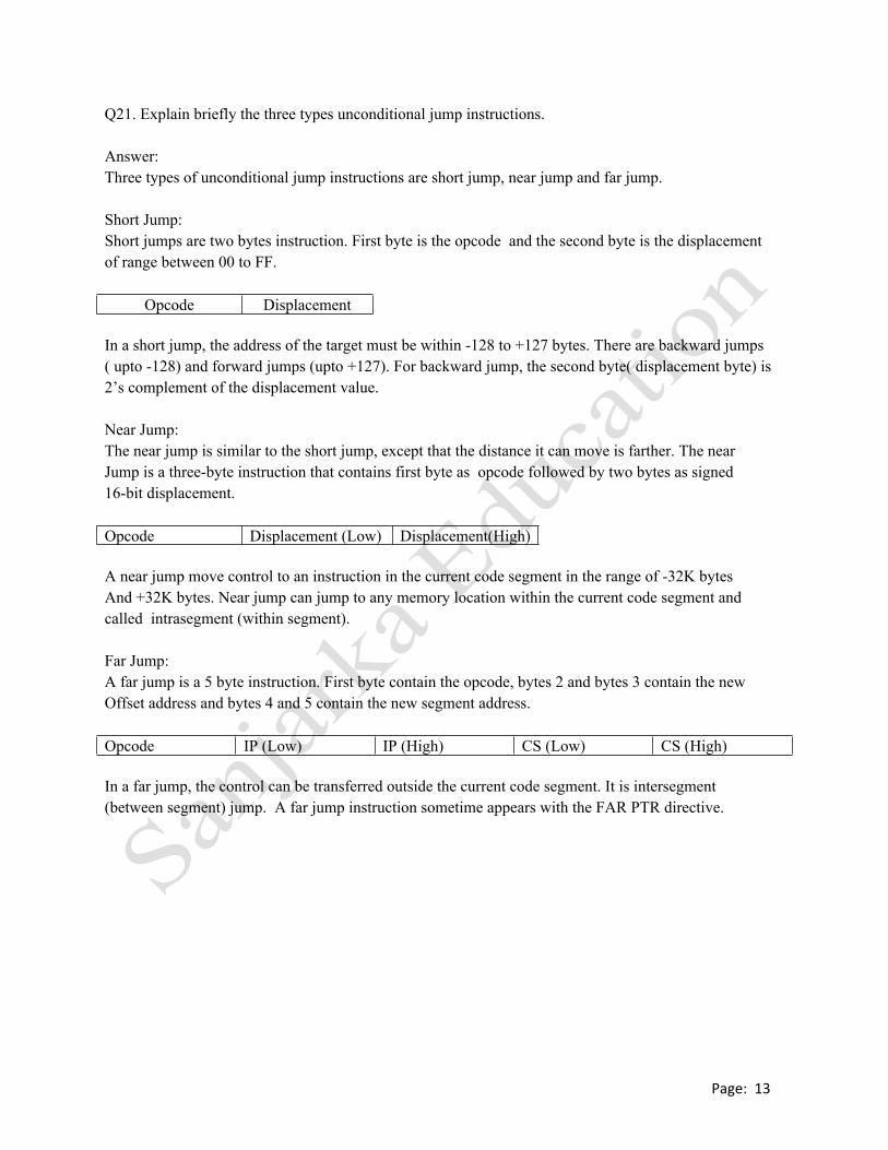
Q21. Explain briefly the three types unconditional jump instructions.
Answer: Three types of unconditional jump instructions are short jump, near jump and far jump.
Short Jump: Short jumps are two bytes instruction. First byte is the opcode and the second byte is the displacementof range between 00 to FF.
Opcode Displacement
In a short jump, the address of the target must be within -128 to +127 bytes. There are backward jumps ( upto -128) and forward jumps (upto +127). For backward jump, the second byte( displacement byte) is 2’s complement of the displacement value.
Near Jump:The near jump is similar to the short jump, except that the distance it can move is farther. The near Jump is a three-byte instruction that contains first byte as opcode followed by two bytes as signed16-bit displacement.
Opcode Displacement (Low) Displacement(High)
A near jump move control to an instruction in the current code segment in the range of -32K bytesAnd +32K bytes. Near jump can jump to any memory location within the current code segment andcalled intrasegment (within segment).
Far Jump:A far jump is a 5 byte instruction. First byte contain the opcode, bytes 2 and bytes 3 contain the new Offset address and bytes 4 and 5 contain the new segment address.
Opcode IP (Low) IP (High) CS (Low) CS (High)
In a far jump, the control can be transferred outside the current code segment. It is intersegment (between segment) jump. A far jump instruction sometime appears with the FAR PTR directive.

Page: 14
Q22. Discuss the conditional jump instructions for 8086 microprocessor.
Answer: Following table shows the various conditional jump instructions for 8086Mnemonic Condition tested OperationJA/JNBE CF=0 and ZF=0 Jump if above / Jump if neither below nor equalJAE/JNB CF=0 Jump if above or equal / Jump if not belowJB/JNAE CF=1 Jump if below / Jump if neither above nor equal JBE/JNA CF=1 or ZF=1 Jump if below or equal/ Jump if not aboveJC CF=1 Jump if carry flag is setJE/JZ ZF=1 Jump if equal / Jump if zeroJG/JNLE ZF=0 and SF=0 Jump if greater thanJGE/JNL SF=0 Jump if greater than or equal/ Jump if not less thanJL/JNGE SF<>0 Jump if less than / Jump if not greater JLE/JNG ZF=1 or SF<>0 Jump if less than or equal / Jump if not greaterJNC CF=0 Jump if no carryJNE/JNZ ZF=0 Jump if not equal / Jump if not zeroJNO OF=0 Jump if no overflowJNP/JPO PF=0 Jump if not parity / Jump if parity oddJNS SF=0 Jump if no signJO OF=1 Jump if overflow s setJP/JPE PF=1 Jump if parity is set / Jump if parity evenJS SF=1 Jump if sign is setJCXZ CX=0 Jump if CX is zero
Q23. Explain briefly the CALL instruction for 8086 microprocessor.Answer: The CALL instruction transfers the flow of the program to the procedure. The CALL instructiondiffers the jump instruction because a CALL instruction saves the return address on the stack. CALL instruction returns the control as per the address saved on the stack when RET is executed.There are two types of CALL; these are Near CALL and Far CALL.Near CALL:The near CALL instruction is three bytes long; the first byte contains opcode, and second and third bytesContain the displacement in the range of -32K to +32K in the 8086.Opcode Displacement (Low) Displacement(High)When the near CALL is executed, it first pushes the offset address of the next instruction on the stack.The offset of the next instruction appears in the instruction pointer (IP). After saving the return address, it then adds the displacement from bytes 2 and 3 to the IP to transfer the control to the procedure.Far CALL: The far CALL is a five-byte instruction that contains an opcode, followed by new contents of the IPand CS. Bytes 2 and 3 contains the new contents of the IP and bytes 4 and 5 contains the new contentsfor CS. Opcode IP (Low) IP (High) CS (Low) CS (High)The far CALL instruction places the contents of both IP and CS on the stack before jumping to theaddress indicated by the bytes 2 to 5 of the instruction. This allows the CALL to call a procedure anywhere in the memory and return from that procedure.

Page: 15
Q24. Explain briefly the following data directives with examples.
(a) ORG (b) DB (c)DUP (d) DW (e) EQU (f) DD (g) DQ (h) DT Answer: (a) ORG:ORG (Origin) is used to indicate the beginning of the offset address. The number that comes after ORGCan be either in hexadecimal or in decimal.For example, ORG 30H ORG 100D(b) DB: DB (Define Byte) allows allocation of memory in byte-sized chunks. DB can be used to define numbers in decimal, binary, hexadecimal and ASCIIFor example, DB 25D DB 10001001B DB 12H DB ‘A’(c) DUP:DUP (Duplicate) is used to duplicate a given numbers of characters. For example, DATA6 DB 6 DUP(0FFH); Fill 6 bytes with FFH(d) DW
DW(Define Word) is used allocate 2 bytes (one word) at a time. For example, DATA0 DW 245AH (e) EQUEQU (Equate) is used to define a constant without occupying a memory location. EQU does not set aside storage for the data item but associate a constant value with a data label .For example, COUNT EQU 25(f) DD: DD (Define Doubeword) is the directive to allocate memory locations that are 4 bytes in size. The can be in decimal, binary or hexadecimal. For example, DATA1 DD 45731023 ; Decimal DATA2 DD 10011100110011111001110011001111B ; BinaryDATA3 DD 5CDA67ACH ;Hexadecimal (g) DQ: DQ(Define quadword) is used to locate 8 bytes (four words) in size. For example, DATA 4 DQ 34H(h) DT:DT(Define ten bytes) is used memory allocation of packed BCD numbers.For example, DATA5 DT 45328965 ;BCD

Page: 16
Q25. Write an assembly language program (ALP) to multiply two 16-bit binary numbers to give 32-bit
result using full segment definition.
Answer: Following is an ALP to multiply two 16-bit binary numbers using full segment definition
DATA_HERE SEGMENT
MULTIPLICAND DW 3B2AH ;First word here
MULTIPLIER DW 204AH ; Second word here
PRODUCT 2 DUP(0) ; Result of the multiplication here
DATA_HERE ENDS
CODE_HERE SEGMENT
ASSUME CS:CODE_HERE, DS:DATA_HERE
START: MOV AX, DATA_HERE ; initialize DS register
MOV DS,AX
MOV AX, MULTIPLICAND ; Get the first word
MUL MULTIPLIER ; Multiply by the second word
MOV PRODUCT, AX ; Store the low word of the result
MOV PRODUCT+2, DX ; Store the high word of the result
INT 3 ; Wait for command from user
CODE_HERE ENDS
END START

Page: 17
Q26. Write an assembly language program (ALP) add a profit factor to each of the 8-elements in a COST
Array and put the result in a PRICES array using full segment definition.
Answer: Following is an ALP add a profit factor to each of the 8-elements in a COST Array and put the
result in a PRICES array using full segment definition.
PROFIT EQU 15H ; profit = 15H
DATA_HERE SEGMENT
COST DB 20H, 28H, 15H, 26H, 19H, 27H, 16H, 29H
PRICES DB 8 DUP(0)
DATA_HERE ENDS
CODE_HERE SEGMENT
ASSUME CS:CODE_HERE, DS:DATA_HERE
START: MOV AX,DATA_HERE ; Initialize the data segment
MOV DS,AX
MOV CX,0008H ;Initialize the counter
MOV BX,0000H ; Initialize the pointer
DO_NEXT: MOV AL, COST[BX] ; Get the cost
ADD AL,PROFIT ; Add the profit
DAA ;Decimal adjust
MOV PRICES[BX],AL ;Store the result in price
INC BX ;Point to next element
DEC CX ; decrement the counter
JNZ DO_NEXT ;If not the last element, do agian
CODE_HERE ENDS
END START

Page: 18
Q27. Draw the commonly used flowchart symbols
Answer: Following are the commonly used Flowchart symbols:
Terminal
Process
Decision
?
Subroutine
Input/ output
Connector

Page: 19
Q28. Draw a flowchart to add 5 bytes and store the result in SUM. Also write the pseudo code.
Answer: Following is the flowchart to add 5 bytes and store the result in SUM.
?
Start
Count=5
Add one byte
Increment pointer
Decrement counter
Count=0YesNo
StoreSUM
Stop
Pseudo code:Count=5 Repeat Add next byte Increment Pointer Decrement Count Until Count=0 Store SUM

Page: 20
Q29. Write ALP program that adds 5 bytes of data and saves the result. The data should be the following hex numbers 25h,12h,15h,1fhand 2bh.Answer: .model small . stack 64 .data data_in db 25h,12h,15h,1fh,2bh sum dw .code mov ax,@data mov ds,ax mov cx,05 mov bx,offset data_in mov ax,0again: add ax,[bx] inc bx dec cx
jnz againmov sum,axmov ah,4chend
Q30. Write ALP program that adds 4 words of data and saves the result. The data should be the following hex numbers 234dh, 1de6h, 3bc7h, 1fh and 566ah.Answer: .model small . stack 64 .data data_in dw 234dh,1de6h,3bc7h,566ah sum dw .code mov ax,@data mov ds,ax mov cx,04 mov bx,offset data_in mov ax,0again: add ax,[bx] inc bx inc bx dec cx
jnz againmov sum,axmov ah,4chend

Page: 21
Q31. Write ALP program that transfer 6 bytes of data from memory locations with offset of 0010h to memory locations with offset of 0028h.Answer: .model small
.stack 64
.dataorg 10h
data_in db 25h, 4fh, 85h, 1fh, 2bh, 1ch org 28h
data_copy db 6 dup(?).codemov ax,@datamov ds,axmov si,offset data_inmov di,offset data_copymov cx.06
again: mov al,[si]mov [di],alinc siinc didec cxjnz againmov ah,4chint 21hend

Page: 22
Q32. Write ALP program to count the number of 1s in a word. Provide the count in BCD.Answer: .model small
.stack 64
.datadataw dw 97b2hcount db ?.codemov ax,@datamov ds,axmov al,0 ;Clear the AL register to keep the number of 1s in BCD.mov dl,16 ;Rotate 16 timesmov bx,dataw
again: rol bx,1 jnc next
add al,1 next: dec dl
jnz againdaamov count,almov ah,4chint 21hend