
Pulse Width Modulator duty
23
Chapter 13 – M68HCS12 Timer 13-49 CLKSEL – Base + $0039 – CRG Clock Select Register Bit 7 6 5 4 3 2 1 0 Read: Write: PLLSEL PSTP SYSWAI ROAWAI PLLWAI CWAI RTIWAI COPWAI Reset: 0 0 0 0 0 0 0 0 RTIWAI RTI Stops in Wait Mode 0 = RTI keeps running in wait mode (default). 1 = RTI stops and initializes the RTI dividers whenever the microcontroller goes into wait mode. See Section 13.8 PLLSEL, PSTP, SYSWAI, ROAWAI, PLLWAI, CWAI, COPWAI PLLSEL – PLL Select Bit. PSTP – Pseudo Stop Bit. SYSWAI – System Clocks Stop in Wait Mode. ROAWAI – Reduced Oscillator Amplitude in Wait Mode. PLLWAI – PLL Stops in Wait Mode. COPWAI – COP Stops in Wait Mode. See Chapter 20 for the details of these bits. 13.10 Pulse-Width Modulator The HCS12 has a pulse-width modulation (PWM) module giving up to six independent pulse-width modulated waveforms. After the PWM module has been initialized and enabled, PWM waveforms will be output automatically with no further action required by the program. This is very useful in applications such as controlling stepper motors. Figure 13-9 shows a pulse-width modulated waveform. There are two times that must be specified and controlled. These are the period (t PERIOD ) and the time the output is high (t DUTY ). A term used to describe a pulse-width modulated waveform is duty cycle . Duty cycle is defined as the ratio of t DUTY to t PERIOD and is usually given as a percent. % 100 × = PERIOD DUTY t t Cycle Duty t DUTY t PERIOD PWM Port Pin Figure 13-9 Pulse-width modulation waveform The HCS12 can output pulse- width modulated waveforms continuously without causing program overhead.
-
Upload
yc2levgmail -
Category
Education
-
view
28 -
download
0
Transcript of Pulse Width Modulator duty

Chapter 13 – M68HCS12 Timer 13-49
CLKSEL – Base + $0039 – CRG Clock Select Register
Bit 7 6 5 4 3 2 1 0
Read: Write:
PLLSEL PSTP SYSWAI ROAWAI PLLWAI CWAI RTIWAI COPWAI
Reset: 0 0 0 0 0 0 0 0 RTIWAI RTI Stops in Wait Mode
0 = RTI keeps running in wait mode (default). 1 = RTI stops and initializes the RTI dividers whenever the microcontroller goes into wait mode.
See Section 13.8
PLLSEL, PSTP, SYSWAI, ROAWAI, PLLWAI, CWAI, COPWAI PLLSEL – PLL Select Bit.
PSTP – Pseudo Stop Bit. SYSWAI – System Clocks Stop in Wait Mode. ROAWAI – Reduced Oscillator Amplitude in Wait Mode. PLLWAI – PLL Stops in Wait Mode. COPWAI – COP Stops in Wait Mode. See Chapter 20 for the details of these bits.
13.10 Pulse-Width Modulator The HCS12 has a pulse-width modulation (PWM) module giving up to six independent pulse-width modulated waveforms. After the PWM module has been initialized and enabled, PWM waveforms will be output automatically with no further action required by the program. This is very useful in applications such as controlling
stepper motors. Figure 13-9 shows a pulse-width modulated waveform. There are two times that
must be specified and controlled. These are the period (tPERIOD) and the time the output is high (tDUTY). A term used to describe a pulse-width modulated waveform is duty cycle. Duty cycle is defined as the ratio of tDUTY to tPERIOD and is usually given as a percent.
%100×=PERIOD
DUTY
tt
CycleDuty
t DUTY
t PERIOD
PWM PortPin
Figure 13-9 Pulse-width modulation waveform
The HCS12 can output pulse-width modulated waveforms continuously without causing program overhead.

Chapter 13 – M68HCS12 Timer 13-50
A simplified block diagram of the pulse-width modulator in the HCS12 is shown in Figure 13-10. An 8-bit (or 16-bit) counter, PWMCNTn4, is clocked by a clock signal. This clock is derived by dividing the system bus clock by a prescaler and other division logic and there are two clock choices for each PWM channel. There are two registers that control the period, PWMPERn, and the duty cycle, PWMDTYn. The system must be initialized with values in these two registers and a clock frequency must be selected. When PWMCNTn is reset, the pulse-width modulator output, PWMn, is set high (or low, depending on the PPOLn polarity control bit). PWMCNTn counts up and when it matches the value in PWMDTYn, the 8-bit Duty Cycle Comparator causes the output to go low (or high). As PWMCNTn continues to count, it ultimately matches the value in the 8-bit Period Comparator that sets the output high (or low) again and resets PWMCNTn to start the process over.
The hardware shown in Figure 13-10 gives a left-aligned pulse as shown in Figure 13-11(a). Center-aligned pulses are available as shown in Figure 13-11(b) as well. Slightly different hardware is used but the concept of registers defining the duty cycle and the period is the same.
Figure 13-12 shows three pulse-width modulated waves with 25%, 50% and 75% duty cycle signals running simultaneously. Figure 13-12(a) illustrates left-aligned pulses and Figure 13-12(b) center-aligned. If it is not necessary for the signals to be aligned as shown in (a), the center-aligned pulses will result in less system noise because all outputs are not switching at the same time.
The pulse-width modulation registers and the counter may be concatenated in pairs to give 16-bit timing resolution. For example, the PWMCNT registers for channels five and four, two and three, and one and zero can be concatenated. This gives a longer period and higher duty cycle resolution than can be achieved with the normal 8-bit operation. A control bit in one of the registers can be set to enable 16-bit operation. You may have six 8-bit, three 16-bit, or any combination of PWM registers.
ProgrammableDivider and
Clock SelectLogic
PWMDTYn Register
PWMCNTn Register
PWMPERn Register
8-BITDuty CycleComparator
8-BITPeriod
Comparator
Bus Clock
ToggleFLIP-FLOP
T Q
QR
MUX
PPOLn
'PWMPOL'
PWMn
RESET
CLOCK A, CLOCK SA,CLOCK B, CLOCK SB
Figure 13-10 Simplified block diagram of the pulse-width modulator for left-aligned pulses.
4 n is 0 - 5. A 16-bit counter may be contrived by combining two, 8-bit PWMCNTn registers.

Chapter 13 – M68HCS12 Timer 13-51
PPOL = 0
PPOL = 1
PWMDTY
PWMPER
(a)
PPOL = 0
PPOL = 1
2 x PWMPER
PWMDTY PWMDTY
(b)
PWMPER
Figure 13-11 (a) Left-aligned and (b) center-aligned pulse-width modulator waveforms.
25%
50%
75%
(a)
25%
50%
75%
(b) Figure 13-12 25%, 50% and 75% duty cycle pulses. (a) Left-aligned pulses. (b) Center-aligned pulses.
Pulse-Width Modulator Clock Control Initializing the PWM module selects the clock rate, the polarity of the output, left- or center-aligned pulses, and which of the PWM outputs are enabled.
There are four clock sources derived from the system bus clock. These are Clock A, Clock B, Clock SA, and Clock SB. Bits in the PWM Prescale Clock Register - PWMPRCLK register control
the divider stages for Clock A and Clock B. These two, independent clocks may be slower than the bus clock by a factor of 1, 2, 4, 8, 16, 32, 64 or 128.
You must select a clock frequency and calculate values for PWMPER and PWMDTY registers when initializing the pulse-width modulator.

Chapter 13 – M68HCS12 Timer 13-52
PWMPRCLK – Base + $00E3 – PWM Prescale Clock Select Register
Bit 7 6 5 4 3 2 1 0
Read: 0 0 Write:
PCKB2 PCKB1 PCKB0
PCKA2 PCKA1 PCKA0
Reset: 0 0 0 0 0 0 0 0 = reserved, unimplemented or cannot be written to. Read: Anytime. Write: Anytime. If these bits are changed while a PWM signal is being generated, a truncated or
stretched pulse may occur. PCKB2:PCKB0, PCKA2:PCKA0 Prescaler bits for Clock A and Clock B
Table 13-12 PWM Clock B and Clock A Prescaler Select Bits
PCKB2 PCKA2
PCKB1 PCKA1
PCKB0 PCKA0
Value of Clock B Value of Clock A
0 0 0 0 1 1 1 1
0 0 1 1 0 0 1 1
0 1 0 1 0 1 0 1
Bus clock Bus clock/2 Bus clock/4 Bus clock/8
Bus clock/16 Bus clock/32 Bus clock/64 Bus clock/128
Clock SA and SB are scaled versions of Clock A and B and are produced by further
dividing Clock A and Clock B by twice the value in PWMSCLA (for Clock SA) and PWMSCLB (for Clock SB). Clocks SA and SB may be anywhere from 1/2 to 1/512th the frequency of Clock A and Clock B. One of these four clocks must be selected by the clock select logic to be used by PWM channels 0 through 5. This is done by bits in the PWM Clock Select Register – PWMCLK and each channel has a choice of two clocks as shown in Table 13-13.
PWMSCLA – Base + $00E8 – PWM Scale A Register
PWMSCLB – Base + $00E9 – PWM Scale B Register
Bit 7 6 5 4 3 2 1 0
Read:
Write:
Reset: 0 0 0 0 0 0 0 0 = reserved, unimplemented or cannot be written to. Read: Anytime. Write: Anytime. Clock A and Clock B Scaling Bits
These registers contain the programmable scaling value for Clock A and Clock B to produce Clocks SA and SB. Clock SA/SB are generated by taking Clock A/B and dividing by twice the value in PWMSCLA/PWMSCLB. When a regis ter is $00, the scale value is 512.
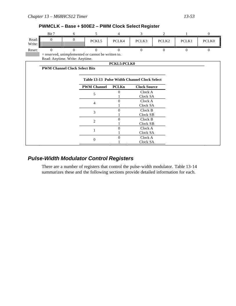
Chapter 13 – M68HCS12 Timer 13-53
PWMCLK – Base + $00E2 – PWM Clock Select Register
Bit 7 6 5 4 3 2 1 0
Read: 0 0 Write:
PCKL5 PCLK4 PCLK3 PCLK2 PCLK1 PCLK0
Reset: 0 0 0 0 0 0 0 0 = reserved, unimplemented or cannot be written to. Read: Anytime. Write: Anytime. PCKL5:PCLK0 PWM Channel Clock Select Bits
Table 13-13 Pulse Width Channel Clock Select
PWM Channel PCLKn Clock Source 0 Clock A 5 1 Clock SA 0 Clock A 4 1 Clock SA 0 Clock B 3 1 Clock SB 0 Clock B 2 1 Clock SB 0 Clock A 1 1 Clock SA 0 Clock A 0 1 Clock SA
Pulse-Width Modulator Control Registers There are a number of registers that control the pulse-width modulator. Table 13-14 summarizes these and the following sections provide detailed information for each.

Chapter 13 – M68HCS12 Timer 13-54
Table 13-14 PWM Control Registers
Register Name Address (Base + ) Function
PWME PWMPOL PWMCLK PWMPRCLK PWMCAE PWMCTL PWMTST PWMPRSC PWMSCLA PWMSCLB PWMSCNTA PWMSCNTB PWMCNT0 PWMCNT1 PWMCNT2 PWMCNT3 PWMCNT4 PWMCNT5 PWMPER0 PWMPER1 PWMPER2 PWMPER3 PWMPER4 PWMPER5 PWMDTY0 PWMDTY1 PWMDTY2 PWMDTY3 PWMDTY4 PWMDTY5
PWM Enable PWM Polarity PWM Clock Select PWM Prescale Clock Select PWM Center Align PWM Control PWM Test PWM Prescale Counter PWM Scale A PWM Scale B PWM Scale A Counter PWM Scale B Counter PWM Channel 0 Counter PWM Channel 1 Counter PWM Channel 2 Counter PWM Channel 3 Counter PWM Channel 4 Counter PWM Channel 5 Counter PWM Channel 0 Period PWM Channel 1 Period PWM Channel 2 Period PWM Channel 3 Period PWM Channel 4 Period PWM Channel 5 Period PWM Channel 0 Duty PWM Channel 1 Duty PWM Channel 2 Duty PWM Channel 3 Duty PWM Channel 4 Duty PWM Channel 5 Duty
$00E0 $00E1 $00E2 $00E3 $00E4 $00E5 $00E6 $00E7 $00E8 $00E9 $00EA $00EB $00EC $00ED $00EE $00EF $00F0 $00F1 $00F2 $00F3 $00F4 $00F5 $00F6 $00F7 $00F8 $00F9 $00FA $00FB $00FC $00FD
PWM Enable. Enables or disables each PWM channel. Polarity select bits for each channel. Selects which of two clock sources is to be used. Sets prescaler value for Clock A and Clock B. Selects left-aligned or center-aligned pulses. Concatenation (16-bit) control and stop mode control. For factory testing only. For factory testing only. PWM scale register for Clock SA. PWM scale register for Clock SB. For factory testing only. For factory testing only. 8-bit, up/down counters for channels 0 – 5. 8-bit period definition registers for channels 0-5 8-bit duty cycle definition registers for channels 0-5.
Pulse-Width Modulation Enable
PWM channel enable bits PWMEN5 – PWME0 in the PWME register allow the selected clock signal to be gated to the PWM. If all channels are disabled, the clock prescaler shuts off to reduce power consumption.

Chapter 13 – M68HCS12 Timer 13-55
PWME – Base + $00E0 – PWM Enable Register Bit 7 6 5 4 3 2 1 0
Read: 0 0 Write:
PWME5 PWME4 PWME3 PWME2 PWME1 PWME0
Reset: 0 0 0 0 0 0 0 0 = reserved, unimplemented or cannot be written to. Read: Anytime. Write: Anytime. PWME5:PWME0 Pulse Width Modulation Channel Enable
When a PWM channel is enabled, the signal becomes available at the output bit when the clock source begins its next cycle.
Table 13-15 Pulse Width Channel Enable
PWM Channel
PWMEn
0 PWM Channel 5 enabled. 5 1 PWM Channel 5 disabled.
0 PWM Channel 4 enabled. If CON45 = 1, PWME4 has no effect and the channel is disabled. 4
1 PWM Channel 4 disabled. 0 PWM Channel 3 enabled. 3 1 PWM Channel 3 disabled.
0 PWM Channel 2 enabled. If CON23 = 1, PWME2 has no effect and the channel is disabled. 2
1 PWM Channel 2 disabled. 0 PWM Channel 1 enabled. 1 1 PWM Channel 1 disabled.
0 PWM Channel 0 enabled. If CON01 = 1, PWME1 has no effect and the channel is disabled. 0
1 PWM Channel 0 disabled.
PWM Polarity Control
The starting polarity of each of the PWM channels is controlled by the PPOLn bits in the PWMPOL register. If the polarity bit is one, the output is high at the beginning of the cycle and then goes low at the end of the duty time. The opposite is true if the PPOLn bit is zero.

Chapter 13 – M68HCS12 Timer 13-56
PWMPOL – Base + $00E1 –Register
Bit 7 6 5 4 3 2 1 0
Read: 0 0 Write:
PPOL5 PPOL4 PPOL3 PPOL2 PPOL1 PPOL0
Reset: 0 0 0 0 0 0 0 0 = reserved, unimplemented or cannot be written to. Read: Anytime. Write: Anytime. If the polarity bit is changes while a PWM signal is being generated, a truncated
or stretched pulse may occur. PPOL5:PPOL0 PWM Output Polarity
0 = The associated channel is low at the beginning of the period and goes high when the duty count is reached (default).
1 = The associated channel is high at the beginning of the period and goes low when the duty count is reached.
PWM Center-Alignment Control
Left-aligned or center-aligned pulse-width modulated waveforms as shown in Figure 13-11 may be generated. Notice that with center-aligned pulses the period is twice the time given by the value in the PWMPER register. The alignment is controlled by the PWMCAE register.
PWMCAE – Base + $00E4 – PWM Center Align Enable Register Bit 7 6 5 4 3 2 1 0
Read: 0 0 Write:
CAE5 CAE4 CAE3 CAE2 CAE1 CAE0
Reset: 0 0 0 0 0 0 0 0 = reserved, unimplemented or cannot be written to. Read: Anytime. Write: Anytime but write only when the corresponding channel is disabled. CAE5:CAE0 Center Aligned Output Enable
0 = Associated channel operates in left-aligned mode (default). 1 = Associated channel operates in center-aligned mode.
PWM Concatenate Control Register
Channels 4 and 5, 2 and 3, and 0 and 1 can be concatenated to create 16-bit PWMs. The high bytes, low bytes and other control bits are specified in Table 13-16. A 16-bit PWM can have longer periods and greater time resolution than an 8-bit pulse modulator.

Chapter 13 – M68HCS12 Timer 13-57
PWMCTL – Base + $00E5 – PWM Control Register Bit 7 6 5 4 3 2 1 0
Read: 0 0 0 Write:
CON45 CON23 CON01 PSWAI PFRZ
Reset: 0 0 0 0 0 0 0 0 = reserved, unimplemented or cannot be written to. Read: Anytime. Write: Anytime. CON45, CON23, CON01 Concatenate Control Bits
0 = Channels are separate 8-bit PWMs. 1 = Channels are combined to be 16-bit PWMs.
Table 13-16 PWM Concatenate Controls
High Byte
Low Byte
Output Pin
Clock Select
Polarity Bit
Enable Bit
Center Alignment
Bit CON45 = 1 CON23 = 1 CON01 = 1
Ch 4 Ch 2 Ch 0
Ch 5 Ch 3 Ch 1
PWM5 PWM3 PWM1
PCLK5 PCLK3 PCLK1
PPOL5 PPOL3 PPOL1
PWME5 PWME3 PWME1
CAE5 CAE3 CAE1
PSWAI PWM Stops in Wait Mode
0 = Allow the clock to the prescaler to continue while in wait mode (default). 1 = Stop the clock when in wait mode. Enabling this allows for lower power consumption when
in wait mode.
PFRZ PWM Counters Stop in Freeze Mode
0 = Allow PWM to continue in freeze mo de (default). 1 = Disable the clock to the prescaler when in freeze mode.
PWM Channel Counter Registers
Each channel has a dedicated 8-bit up/down counter which runs at the selected clock source rate. The counter can be read at any time without affecting the PWM waveform. In left-aligned mode the counter starts at $00 and counts to the value in the period register minus one (PWMPERn – 1). In center-aligned mode the counter counts from $00 up to the value in the period register and then back down to $00.

Chapter 13 – M68HCS12 Timer 13-58
PWMCNT0 – Base + $00EC – Counter Channel 0 Register
PWMCNT1 – Base + $00ED – Counter Channel 1 Register
PWMCNT2 – Base + $00EE – Counter Channel 2 Register
PWMCNT3 – Base + $00EF – Counter Channel 3 Register
PWMCNT4 – Base + $00F0 – Counter Channel 4 Register
PWMCNT5 – Base + $00F1 – Counter Channel 5 Register
Bit 7 6 5 4 3 2 1 0
Read: Write: 0 0 0 0 0 0 0 0
Reset: 0 0 0 0 0 0 0 0 = reserved, unimplemented or cannot be written to. Read: Anytime. Write: Anytime (any value written causes PWM counter to be reset to $00). PWM Channel Counters
The channel counters contain the current count against which the channel period registers (PWMPERn) and the duty cycle registers (PWMDTYn) are compared.
A counter is reset to $00 and the direction is set to up anytime it is written. At this time the duty and period registers are loaded and the output changed according to the polarity bit.
The counter is cleared at the end of a period. To avoid a truncated period, you should write to the PWMCNTn register when the counter is disabled. If a counter channel is disabled (PWMEn = 0), the PWMCNTn register does not count. If you disable a PWM counter and then enable it again, the PWM channel counter starts at the count in
the PWMCNTn register. The counter may be read at any time without affecting the value of the counter.
PWM Period and Duty Registers
As you can see in Error! Reference source not found., the values in the PWMPERn and PWMDTYn registers control length of the period and the active high or low time of the pulse modulated waveform.

Chapter 13 – M68HCS12 Timer 13-59
PWMPER0 – Base + $00F2 – Channel 0 Period Register
PWMPER1 – Base + $00F3 – Channel 1 Period Register
PWMPER2 – Base + $00F4 – Channel 2 Period Register
PWMPER3 – Base + $00F5 – Channel 3 Period Register
PWMPER4 – Base + $00F6 – Channel 4 Period Register
PWMPER5 – Base + $00F7 – Channel 5 Period Register
Bit 7 6 5 4 3 2 1 0
Read: Write:
Reset: 0 0 0 0 0 0 0 0 = reserved, unimplemented or cannot be written to. Read: Anytime. Write: Anytime. PWM Channel Period Registers
The channel period registers contain the count specifying the end of the period. If a PWMPERn register is written while the PWM is enabled, the new value will not take effect until
the existing period terminates. To start a new period immediately, write the PWMPERn register and then write to the PWMCNTn
register to reset it to $00 or disable and then enable the channel. PWMPERn can be read at any time to find the most recent value written. The PWM period is as follows:
Left-Aligned Waveform (CAEn = 0): Period = Channel_Clock_Period * (PWMPERn ) Center-Aligned Waveform (CAEn = 1): Period = Channel_Clock_Period * 2 * PWMPERn
Chapter 13 – M68HCS12 Timer 13-60
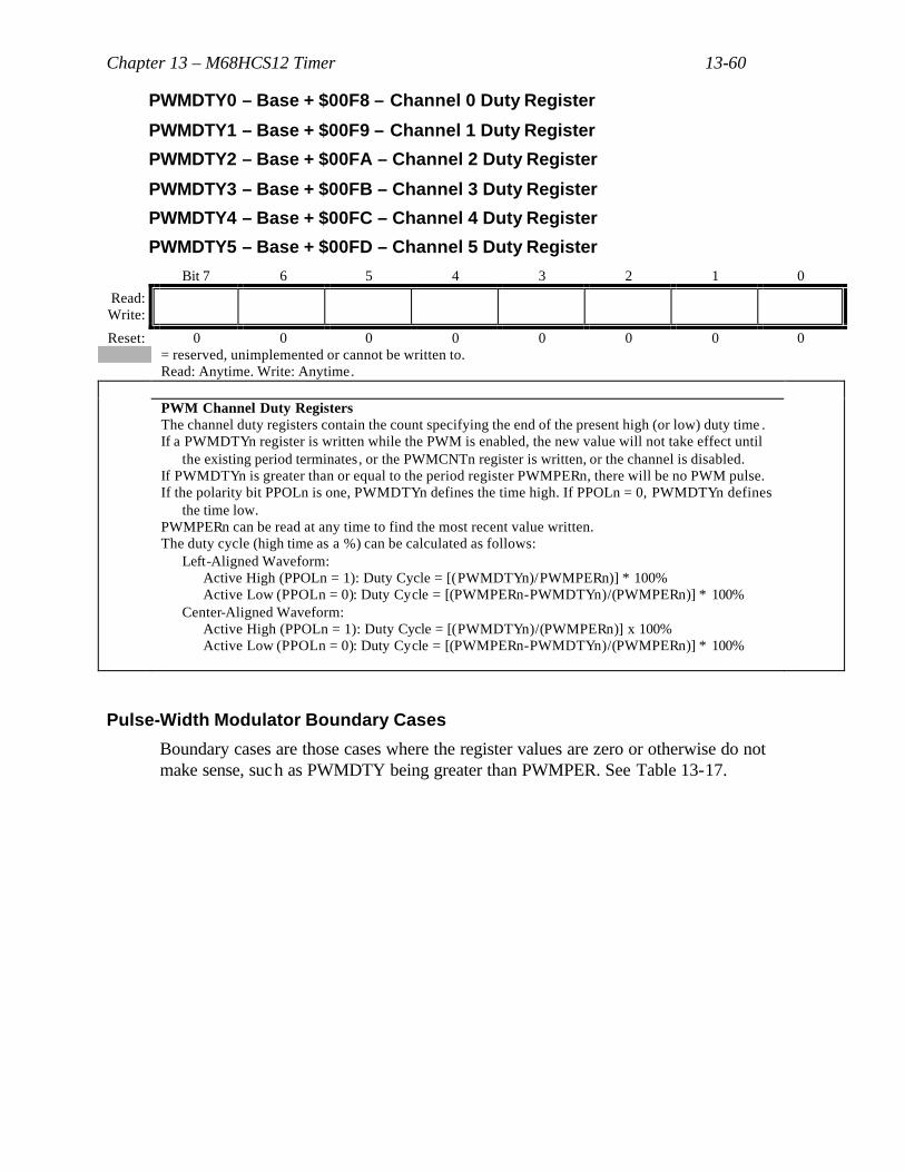
PWMDTY0 – Base + $00F8 – Channel 0 Duty Register
PWMDTY1 – Base + $00F9 – Channel 1 Duty Register
PWMDTY2 – Base + $00FA – Channel 2 Duty Register
PWMDTY3 – Base + $00FB – Channel 3 Duty Register
PWMDTY4 – Base + $00FC – Channel 4 Duty Register
PWMDTY5 – Base + $00FD – Channel 5 Duty Register
Bit 7 6 5 4 3 2 1 0
Read: Write:
Reset: 0 0 0 0 0 0 0 0 = reserved, unimplemented or cannot be written to. Read: Anytime. Write: Anytime. PWM Channel Duty Registers
The channel duty registers contain the count specifying the end of the present high (or low) duty time . If a PWMDTYn register is written while the PWM is enabled, the new value will not take effect until
the existing period terminates, or the PWMCNTn register is written, or the channel is disabled. If PWMDTYn is greater than or equal to the period register PWMPERn, there will be no PWM pulse. If the polarity bit PPOLn is one, PWMDTYn defines the time high. If PPOLn = 0, PWMDTYn defines
the time low. PWMPERn can be read at any time to find the most recent value written. The duty cycle (high time as a %) can be calculated as follows:
Left-Aligned Waveform: Active High (PPOLn = 1): Duty Cycle = [(PWMDTYn)/PWMPERn)] * 100% Active Low (PPOLn = 0): Duty Cycle = [(PWMPERn-PWMDTYn)/(PWMPERn)] * 100%
Center-Aligned Waveform: Active High (PPOLn = 1): Duty Cycle = [(PWMDTYn)/(PWMPERn)] x 100% Active Low (PPOLn = 0): Duty Cycle = [(PWMPERn-PWMDTYn)/(PWMPERn)] * 100%
Pulse-Width Modulator Boundary Cases
Boundary cases are those cases where the register values are zero or otherwise do not make sense, such as PWMDTY being greater than PWMPER. See Table 13-17.

Chapter 13 – M68HCS12 Timer 13-61
Table 13-17 PWM Boundary Cases
PWMDTYn PWMPERn PPOLn PWMn Output $00
Indicates no duty >$00 1 Always Low
$00 Indicates no duty
>$00 0 Always High
XX $005 Indicates no period
1 Always High
XX $00 Indicates no period
0 Always Low
>= PWMPER XX 1 Always High >= PWMPER XX 0 Always Low
Using Port T Outputs for PWM Waveforms On some versions of the MC9S12C microcontroller family, the Port P, PWM pins may not be available for use. In these cases, as we described in Chapter 10, you may switch the PWM outputs to bits on Port T. Of course in these cases, the Port T bit cannot be used for other timer functions. The register in the Port Integration Module that is used to do this is the Port T Module Routing Register – MODRR. In these cases you do not have to set the data direction register for Port T.
MODRR – Base + $0247 – Port T Module Routine Register Bit 7 6 5 4 3 2 1 0
Read: 0 0 0 Write:
MODRR4 MODRR3 MODRR2 MODRR1 MODRR0
Reset: 0 0 0 0 0 0 0 0 = reserved, unimplemented or cannot be written to. Read: Anytime. Write: Anytime. MODRR4:MODRR0 Port T Module Selection Bits
0 = Associated pin is connected to the timer module (default). 1 = Associated pin is connected to the PWM module.
Choosing Pulse-Width Modulation Counter Prescaler and Scaler Values
There are several clock dividers and counter registers that must be initialized befo re using the pulse-width modulators. When PWMs drive motors or other mechanical systems, the PWM frequency (if too low) can cause objectionable audible noise. For this reason, it is important to be able to get the PWM frequency above 20 kHz (not easy or practical in software). If the frequency is too high, though, some components may not be able to follow the rate of change. Another common use of the PWM is to use it to drive an R-C low pass filter to get a crude digital-to-analog converter. In this case the PWM frequency needs to be high enough to be able to choose reasonable resistors and capacitors. Here is
5 Counter = $00 and does not count.

Chapter 13 – M68HCS12 Timer 13-62
a strategy to pick appropriate values for the PWM registers based on the period and duty cycle of the pulse-width modulated waveform.
1. Choose PWMPERn = 256. This gives the best resolution when choosing the duty cycle count for PWMDTYn.
2. Divide tPERIOD by 256. This establishes the period of the PWMCNTn clock.
3. Divide the PWMCNTn period by the bus clock period. This gives the total divisor needed.
If the total divisor is greater than 65,536 - [(128 in the PWMPRCLK prescaler) * (256 in the PWMSCLn clock scale register) * (2)] - 16-bit concatenated registers are needed.
If the total divisor is not an integer, choose the next higher integer value and recalculate the PWMCNTn period.
Recalculate PWMPERn.
4. Calculate the number of counts needed in the PWMDTYn register based on the PWMCNTn period.
If PWMDTYn is not an integer, round up or down to the nearest integer
value. Make sure PWMDTYn ≤ 256 (or 65536).
5. Select an appropriate divider combination to give the total divisor and a clock source to give PWMCNTn. If the total divisor is not a power of two, you will have to use a combination of Clock A and SA or Clock B and SB and PWMSCLn to achieve an exact period and duty cycle. If the total divisor is not an integer, round down to the nearest integer and recalculate PWMPERn and PWMDTYn register values. Again, be sure PWMPERn does not exceed the maximum.
6. If you are using Clock A or Clock B and the total divisor is not a power of 2, choose the nearest value and recalculate PWMPERn and PWMDTYn registers values.
PERIOD
PWMCNT
ClockBusT
DivisorTotal =
PERIODPWMCNT ClockBusDivisorTotalT *=
PWMCNT
PERIOD
Tt
PWMPER =
PWMCNT
DUTY
Tt
PWMDTY =
256PERIOD
PWMCNTt
T =

Chapter 13 – M68HCS12 Timer 13-63
Example 13-26
Choose values for the PWMDTY1, PWMPER1, and PWSCLN registers , and the PCKA2:PCKA0, PCKB2:PCKB0, PPOL1, CAE1 and CON01 control bits to generate a pulse-width modulated waveform on PWM channel 1 with a frequency of 20 KHz and a high duty cycle time of 10 µs. Assume the bus clock is 8 MHz.
Solution:
1. The tperiod is 50 µs.
2. Choose PWMPER1 = 256 and calculate the period of the PWMCNT1 clock:
TPWMCNT1 = tPERIOD/256 = 50 µs/256 = 0.1953 µs
3. Calculate the Total Divisor required:
Total Divisor = TPWMCNT1/Bus ClockPERIOD = 0.193 µs/0.125 µs = 1.56
Not an integer, so choose Total Divisor = 2.
4. Recalculate TPWMCNT1:
TPWMCNT1 = Total Divisor * Bus ClockPERIOD = 2 * 0.125 µs = 0.25 µs
5. Recalculate PWMPER1:
PWMPER1 = tPERIOD/TPWMCNT1 = 50 µs/0.25 µs = 200
6. Calculate the number of counts required in PWMDTY1 for 10 µs.
PWMDTY1 = tDUTY/TPWMCNT1 = 10 µs/0.25 µs = 40
7. Choose a divisor combination to achieve a total divisor = 2. This can be done by choosing Clock A.
Clock A = Bus Clock/Prescaler
For a total divisor of 2, choose the prescaler = 2.
The control bits are:
PCKA2:PCKA0 = %001, PWMSCLA = don't care or whatever might be required if Clock SA is used on another channel, PCKB2:PCKB0 are don't cares or whatever might be needed for Clock B, PCLK1 = 0, CON01 = 0, CAE1 = 0 and PPOL1 = 1. See Example 13-30.
Another strategy to pick appropriate values for each register is based on the duty cycle resolution required by the application.
Duty cycle resolution is the smallest unit of time by which tDUTY (Figure 13-9) may change. This may be given as the actual time or as a percent of the full PWM period. Duty cycle resolution determines the minimum count value for the PWMPERn register.
Here is a method to choose PWMPER, PWMDTY, and the clock frequency.
%1001
%100 ∗=∗∆
=PWMPERt
tresolutioncycleDuty
PERIOD
DUTY

Chapter 13 – M68HCS12 Timer 13-64
1. Find the minimum value for the PWMPER register based on the duty cycle resolution. Choose any value greater than this but less than or equal to 256 (or 65536 in a 16-bit system.)
2. Divide tPERIOD by the value chosen for PWMPER. This establishes the period of the PWMCNT clock.
3. Calculate the number of counts needed in the PWMDTY register based on the PWMCNT period.
If PWMDTY is not an integer, choose the next higher va lue and recalculate the PWMCNT period and a new PWMPER value. Make sure PWMPER ≤ 256 (or 65536).
4. Divide the PWMCNT period by the bus clock period. This gives the total divisor needed.
If the total divisor is greater than 65,536 - [(128 in the PWPRES prescaler) * (256 in the PWMSCLn clock scale register) * (2)] - 16-bit concatenated registers are needed.
5. Select an appropriate divider combination to give the total divisor and a clock source to give PWMCNT. If the total divisor is not a power of two, you will have to use a combination of Clock A and SA and PWMSCLA to achieve an exact period and duty cycle. If the total divisor is not an integer, round down to the nearest integer and recalculate PWMPER and PWMDTY register values. Again, be sure PWMPER does not exceed the maximum.
6. If you are using Clock A or Clock B and the total divisor is not a power of 2, choose the nearest value and recalculate PWMPER and PWMDTY registers values.
Example 13-27
Choose values for the PWMDTY1, PWMPER1, and PWSCLn registers, and the PCKA2:PCKA0, PCKB2:PCKB0, PPOL1, CAE1 and CON01 control bits to generate a pulse-width modulated waveform on PWM channel 1 with a period of 20 ms and a high duty cycle time of 7 ms . The duty cycle resolution is to be 0.5%. Assume the bus clock is 8 MHz.
Solution:
1. The required duty cycle resolution is 0.5%. This tells us that the ratio of ?tDUTY to TPERIOD is 1:200 and that an 8-bit PWMPER register should be sufficient. Choose a value of 200 for PWMPER1.
2. Calculate the period of the PWMCNT1 clock:
TPWMCNT1 = tPERIOD/200 = 20 ms/200 = 100 µs
3. Calculate the number of counts required in PWMDTY1 for 7 ms.
PWMDTY1 = tDUTY/TPWMCNT1 = 7 ms/100 µs = 70
Period
PWMCNT
ClockBusT
DivisorTotal =
PWMPERT
T PERIODPWMCNT =
PWMCNT
DUTY
Tt
PWMDTY =

Chapter 13 – M68HCS12 Timer 13-65
4. Calculate the total divisor required.
Total Divisor = TPWMCNT1/Bus ClockPERIOD = 100 µs/0.125 µs = 800
5. Choose a divisor combination to achieve 800. This can be done by choosing Clock SA.
Clock SA = Bus Clock/(Prescaler * PWSCLA * 2)
For a total divisor of 800, choose the prescaler = 16 and PWSCLA = 25 (16 * 25 * 2 = 800). The registers and control bits are: PCKA2:PCKA0 = %100, PWSCLA = 25, PCKB2:PCKB0 are don't cares or whatever might be needed for Clock B, PCLK1 = 1, CON01 = 0, CAE1 = 0 and PPOL1 = 1. See Example 13-32.
Example 13-28
Specify the divider value and PWMPER3 and PWMDTY3 register values for a pulse-width modulated waveform on PWM3 using Clock B. The period is to be 1.8 ms, tDUTY = 0.1 ms, and the duty cycle resolution is to be less than (better than) 1%. Assume the bus clock is 8 MHz. State the final tDUTY , tPERIOD and duty cycle resolution achieved by your design. Calculate the percent error in tDUTY and tPERIOD if the design does not achieve exact timing.
Solution:
1. Duty cycle resolution is 1% . Therefore, PWMPER3 must be ≥ 100. Choose PWMPER3 = 200.
2. Calculate PWMCNT3 period.
TPWMCNT3 = tPERIOD/200 = 1.8 ms/200 = 9 µs.
3. PWMDTY3 = tDUTY/TPWMCNT3 = 0.1 ms/9 µs = 11.1
PWMDTY3 is not an integer, so choose next higher PWMDTY3 = 12.
To achieve tDUTY when PWMDTY3 = 12, TPWMCNT3 = tDUTY /PWMDTYT3 = 0.1 ms/12 = 8.33 µs.
New PWMPER3 = tPERIOD/TPWMCNT3 = 1.8 ms/8.33 µs = 216
4. Total divisor = 8.33 µs/0.125 µs = 66.64.
The next smaller Clock B divisor is 64, so choose that.
5. Recalculate PWMCNT3 period and new values for PWMPER3 and PWMDTY3.
TPWMCNT3 = 0.125 µs * 64 = 8 µs.
PWMPER3 = 1.8 ms/8 µs = 225.
PWMDTY3 = 0.1 ms/8 µs = 12.5. Choose 12.
6. Calculate errors
Final tPERIOD = 225 * 8 µs = 1.8 ms. Error = 0%.
Final tDUTY = 12 * 8 µs = 0.096 ms. Error = (0.1 - 0.096)/0.1 = 4 %.
Duty cycle resolution = 1/225 = 0.4%.

Chapter 13 – M68HCS12 Timer 13-66
Example 13-29
What is the longest PWM period that can be obtained using a single 8-bit PWM register assuming an 8 MHz bus clock and left-aligned waveforms?
Solution:
The longest period is achieved using an 8-bit PWMPER register and the slowest Clock S. The slowest Clock SA or SB is formed by dividing the bus clock by 128 to give Clock A or B and then by setting PWSCAL to $00 which divides Clock A or B by 512. The period is PWMPER times this clock period. Therefore, the longest period is P-clockPERIOD * 128 * 512 * 256 = 2.09 seconds.
Pulse-Width Modulation Software Checklist Here are the steps to check when writing your software for timer output compares:
1. Set the module routing register (MODRR) to route the PWM output to Port T if needed; otherwise, set the Port P bit to be used to output.
2. Choose which clock source is to be used, Clock A or Clock B, and set the total divisor in the PWMPRCLK register.
3. If a scaled clock, Clock SA or Clock SB, is to be used, set the scaler value in PWMSCLA or PWMSCLB.
4. Assign the clock source to the PWM channel being used in PWMCLK.
5. Set the polarity bit in PWMPOL.
6. Enable left-aligned or center-aligned pulses in PWMCAE.
7. Set the period register, PWMPERn.
8. Set the duty register, PWMDTYn.
9. Enable the channel in PWME.
Pulse-Width Modulation Examples
Example 13-30 PWM Waveform using Clock A
Metrowerks HC12-Assembler (c) COPYRIGHT METROWERKS 1987-2003 Rel.Loc Obj. code Source line ---------- --------- ----------- 1 ; This is a test program showing a 2 ; 20 kHz PWM waveform with 10 us high 3 ; duty time. The output is Port T-1. 4 ;******************************** 5 ; Define the entry point for the main program 6 XDEF Entry, main 7 XREF __SEG_END_SSTACK

Chapter 13 – M68HCS12 Timer 13-67
8 INCLUDE pwm.inc ; Timer defns 9 INCLUDE base.inc ; Reg base defn 10 INCLUDE bits.inc ; Bit defns 11 ;******************************** 12 ; Constants 13 0000 00C8 PERIOD: EQU 200 ; PWMPER1 14 0000 0028 DUTY: EQU 40 ; PWMDTY1 15 0000 0001 DIVISOR:EQU %00000001 ; Clk A=BusClock/2 16 ; Code Section 17 MyCode: SECTION 18 Entry: 19 main: 20000000 CFxx xx lds #__SEG_END_SSTACK 21 ; Initialize the I/O 22 ; Set the module routing register to 23 ; route PWM1 to Port T, bit-1 24000003 1C02 4702 bset MODRR,BIT1 25 ; Set Clock A prescaler to divide by 2 26000007 180B 0100 movb #DIVISOR,PWMPRCLK 00000B E3 27 ; Set Clock SA scale register 28 ; (Don't cares, not used) 29 ; Set PWM Channel 1 clock to Clock A 3000000C 4DE2 02 bclr PWMCLK,PCLK1 31 ; Enable active high polarity 3200000F 4CE1 02 bset PWMPOL,PPOL1 33 ; Enable left-aligned pulse 34000012 4DE4 02 bclr PWMCAE,CAE1 35 ; Set the period register 36000015 180B C800 movb #PERIOD,PWMPER1 000019 F3 37 ; Set the duty register 3800001A 180B 2800 movb #DUTY,PWMDTY1 00001E F9 39 ; Enable Channel 1 4000001F 4CE0 02 bset PWME,PWME1 41 42 ; Main loop - do nothing 43 spin: 44000022 20FE bra spin 45 ;********************************
Explanation of Example 13-30
Example 13-30 is a program outputting a 20 kHz PWM waveform with a 10 µs high duty time. The 9S12C32 processor used for this code does not have the PWM output pins so Port T, bit-1 is to be used for the PWM channel 1 output. The MODRR register is initialized to make this switch in line 24. The Clock A prescaler, period and duty times have been calculated as shown in Example 13-26. The Clock A prescaler is initialized in line 26 and Clock A is assigned to PWM channel 1 in line 30. Active-high polarity and left-aligned pulses are selected in lines 31 – 34. The period and duty registers are initialized in lines 35 – 38 and the PWM enabled in line 40. Once the PWM is enabled it starts to generate the waveform and the program enters a main loop, in this case doing nothing.

Chapter 13 – M68HCS12 Timer 13-68
Example 13-31 PWM Waveform in C
/******************************************************************* * Pulse Width Modulation waveform. * This outputs a 20 kHz waveform with a high duty time that varies * from 10 us to 50 us. The output is Port T, bit-1 *******************************************************************/ #include <mc9s12c32.h> /* derivative information */ #define PERIOD 200 #define DUTY 40 /*******************************************************************/ void main(void) { unsigned char duty; /*******************************************************************/ /* Set the module routing register to route PWM1 * to Port T bit-1 */ MODRR_MODRR1 = 1; /* Set Clock A prescaler to divide by 2 */ PWMPRCLK = 1; /* Set Clock SA scale register */ /* Not used in this example */ /* Set PWM Channel 1 clock to Clock A */ PWMCLK_PCLK1 = 0; /* Enable active high polarity */ PWMPOL_PPOL1 = 1; /* Enable left-aligned pulse */ PWMCAE_CAE1 = 0; /* Set the period register */ PWMPER1 = PERIOD; /* Enable Channel 1 */ PWME_PWME1 = 1; /* Scan the output high time from 10 us to 50 us */ for(duty = DUTY;duty <= PERIOD;++duty) { PWMDTY1 = duty; } /* wait forever */ }
Example 13-32 PWM Waveform using Clock SA
Metrowerks HC12-Assembler (c) COPYRIGHT METROWERKS 1987-2003 Rel.Loc Obj. code Source line ---------- --------- ----------- 1 ; This is a test program showing a 2 ; PWM waveform with 20 ms period and 3 ; 7 ms high duty time. The output is on 4 ; Port T-1. 5 ;******************************** 6 ; Define the entry point for the main program 7 XDEF Entry, main 8 XREF __SEG_END_SSTACK 9 INCLUDE pwm.inc ; Timer defns 10 INCLUDE base.inc ; Reg base defn 11 INCLUDE bits.inc ; Bit defns 12 ;******************************** 13 ; Constants

Chapter 13 – M68HCS12 Timer 13-69
14 0000 00C8 PERIOD: EQU 200 ; PWMPER1 15 0000 0046 DUTY: EQU 70 ; PWMDTY1 16 0000 0004 DIVISOR:EQU %00000100 ; Clk A=BusClock/16 17 0000 0019 SCALER: EQU 25 ; Clk SA scaler 18 ; Code Section 19 MyCode: SECTION 20 Entry: 21 main: 22000000 CFxx xx lds #__SEG_END_SSTACK 23 ; Initialize the I/O 24 ; Set the module routing register to 25 ; route PWM1 to Port T, bit-1 26000003 1C02 4702 bset MODRR,BIT1 27 ; Set Clock A prescaler to divide by 2 28000007 180B 0400 movb #DIVISOR,PWMPRCLK 00000B E3 29 ; Set Clock SA scale register 3000000C 180B 1900 movb #SCALER,PWMSCLA 000010 E8 31 ; Set PWM Channel 1 clock to Clock SA 32000011 4CE2 02 bset PWMCLK,PCLK1 33 ; Enable active high polarity 34000014 4CE1 02 bset PWMPOL,PPOL1 35 ; Enable left-aligned pulse 36000017 4DE4 02 bclr PWMCAE,CAE1 37 ; Set the period register 3800001A 180B C800 movb #PERIOD,PWMPER1 00001E F3 39 ; Set the duty register 4000001F 180B 4600 movb #DUTY,PWMDTY1 000023 F9 41 ; Enable Channel 1 42000024 4CE0 02 bset PWME,PWME1 43 ; Main loop - do nothing 44 spin: 45000027 20FE bra spin 46 ;********************************
Explanation of Example 13-32
Example 13-32 is a program outputting a PWM waveform with a 20 ms period and a 7 ms high duty time. The 9S12C32 processor used for this code does not have the PWM output pins so Port T, bit-1 is to be used for the PWM channel 1 output. The MODRR register is initialized to make this switch in line 26. The Clock A prescaler, Clock SA scaler, period and duty times have been calculated as shown in Example 13-27. The Clock A prescaler is initialized in line 28 and the Clock SA scaler in line 30. Clock SA is assigned to PWM channel 1 in line 32. Active-high polarity and left-aligned pulses are selected in lines 33 – 36. The period and duty registers are initialized in lines 37 – 40 and the PWM enabled in line 42. Once the PWM is enabled it starts to generate the waveform and the program enters a main loop, in this case doing nothing.

Chapter 13 – M68HCS12 Timer 13-70
13.11 Conclusion and Chapter Summary Points The timer features of the M68HCS12 are useful in many applications. Although the programming and control of the elements seems complex, the operation of all functions is similar with similar control requirements. The common elements are as follows:
• Timing is derived from the bus clock.
• A common bus clock frequency is 8 MHz.
• The bus clock may be prescaled (divided) by 1, 2, 4, 8, 16 or 32.
• The TEN bit in the TSCR1 register must be set start the timer counting.
• A 16-bit free running counter, TCNT, provides the basic counting functions in the system.
• TCNT generates a timer overflow every 65,536 clock cycles.
• Eight channels of output compare can set an output compare flag when the TCNT register is equal to the output compare register.
• The output compare can automatically change output bits when the comparison is made.
• Timer resolution can be a fine as one bus clock cycle.
• Eight channels of input capture can latch the TCNT on an input signal.
• A pulse accumulator can count external pulses and generate interrupts.
• All timer functions set a flag to indicate when their particular event has occurred.
• Each timer flag can be ANDed with an interrupt enable bit to generate an interrupt when the particular event has occurred.
• In all events, the flag is reset by software writing a one to the flag.
• The timer module has a real-time interrupt that can generate interrupts at a variety of rates.
• The HCS12 has a pulse-width modulator waveform generator.
• Pulse-width modulation waveforms are automatically generated by the hardware without burdening the software.
13.12 Bibliography and Further Reading Cady, F. M., Microcontrollers and Microprocessors, Oxford University Press, New
York, 1997. CPU12 Reference Manual, S12CPUV2.PDF, Freescale Semiconductor, Inc. TIM_16B8C Block User Guide, S12TIM16B8CV1/D.PDF, Freescale
Semiconductor, Inc., October 2001.
Chapter 13 – M68HCS12 Timer 13-71
PWM_8B6C Block User Guide, S12PWM8B6CV1/D, Freescale Semiconductor, Inc., March 2002
More, G. M. and Gallop, M. PWM Generation Using HCS12 Timer Channels, Application Note AN2612, Rev 0, 11/2003, Freescale Semiconductor, Inc., 2003.
More, G. M., Audio Reproduction HCS12 Microcontrollers, Application Note AN2250, Rev 0, 1/2002, Freescale Semiconductor, Inc., 2002.
Morales, A., Using Real-Time Interrupt on HCS12 Microcontrollers, Application Note AN2882, Rev 1, 5/2005, Freescale Semiconductor, Inc., 2005.
13.13 Problems