
PULSE MODE COUNTING SYSTEM WITH PARALLEL PORT …
25
PINSTECH-218 PULSE MODE COUNTING SYSTEM WITH PARALLEL PORT INTERFACE By MUHAMMAD ATHAR FAROOQ NAVEED MUSHTAQ MAJEED SULTAN ABDUL KARIM MANAGEMENT INFORMATION SYSTEM DIVISION DIRECTORATE OF COORDINATION PAKISTAN INSTITUTE OF NUCLEAR SCIENCE & TECHNOLOGY P.O Nilore, Islamabad November, 2010
Transcript of PULSE MODE COUNTING SYSTEM WITH PARALLEL PORT …

PINSTECH-218
PULSE MODE COUNTING SYSTEM WITH PARALLEL PORT INTERFACE
By
MUHAMMAD ATHAR FAROOQ NAVEED MUSHTAQ MAJEED SULTAN
ABDUL KARIM
MANAGEMENT INFORMATION SYSTEM DIVISIONDIRECTORATE OF COORDINATION
PAKISTAN INSTITUTE OF NUCLEAR SCIENCE & TECHNOLOGYP.O Nilore, Islamabad
November, 2010

ABSTRACT
Pulse mode Counting System (PPCS) module has been designed and
developed w h ich is compatible w ith SPP (Standard Para lle l Port) and EPP
(Enhanced Paralle l Port). This system can capture, present and store real time data
in a w e ll fo rm atted form . The stored data is in a fo rm a t tha t can be imported in
different packages fo r fu r th e r analysis. The purpose o f th is system is to fac ilita te
the research experiments having frequency range up to 4 MHz and storing range
up to 16 m illion counts.

Table of Contents
1. Introduction................................................................................................................1
2. Related Work.............................................................................................................. 2
3. Hardware Description of the system.........................................................................3
3.1. Functional Description of P P C S hardware........................................................ 3
3.2 Hardware Description of PPCS...........................................................................4
3.3 Technical Specification of PPCS.........................................................................6
3.4 Interfacing with Centronics Port......................................................................... 6
3.5 Signal Isolation.................................................................................................... 8
3.6 Power Supply ...................................................................................................... 8
3.7 Timer Function....................................................................................................8
3.8 Counter................................................................................................................8
3.8.1 Features of Counter............................................................................................9
4. Software Description of the system...........................................................................9
4.1 Output File Name............................................................................................... 10
4.2 Counting T im e.................................................................................................. 10
4.3 Number of Readings...........................................................................................10
4.4 Current Data.......................................................................................................10
4.5 Readings Remaining........................................................................................... 10
4.6 Input Data Validation.........................................................................................10
4.7 Start....................................................................................................................11
4.8 Exit......................................................................................................................11
4.9 Precautions.........................................................................................................12
5. Conclusion and discussion......................................................................................13
Acknowledgement.......................................................................................................14
6. References............................................................................................................... 15
Appendix A (Parallel Port)...........................................................................................16
A (1) What is Parallel Port....................................................................................16
A (1.1) Port Addresses..................................................................................... 17
A (1.2) Data Port................................................................ ........ 18
A (1.3) Status Port................................................................ .......... 18
A (1.4) Control Port................................................................ ........... 19
Appendix B (Data Sheet of Counter)......................................................................... 20

1. INTRODUCTION
A general requirement in a laboratory environment is the monitoring of certain
events to determine the number of events per unit time. In nuclear experiments, the
signal received from a detector is fed to an amplifier (linear or logarithmic). The output
of the amplifier is connected to the input of a Single Channel Analyzer (SCA). The SCA
output is a logic pulse for each event. These logic pulses are used by the counting
circuitry for count rate measurement. Some of these systems reading displayed by
count rate meter of the experiment is noted manually and then fed to computer for
further processing. It is very tedious, laborious and tiring job and due to manual data
recording, probability of human error factor is quite high.
In many laboratories at PINSTECH only single channel pulse counting is
required so it is not necessary to use a multifunctional and multi-channel counting
system. For example Radioisotope Hydrology Group of Isotopes Application Division
(IAD) is carrying out field experiments for optimization of uranium leach mining
pattern at Taunsa. For this purpose Eberline count rate meter is used. The meter
displays data in counts/sec and the readings have to be noted manually. Group is
interested to get it interfaced with the computer system, so that the experimental data
could be acquired on-line and archived during field experiments. Later on the data
could be transferred to other systems in laboratory for processing and analysis. This
group is also involved in the detection of radioactive traces activities. A Rheometer
system is used for measurement of ground water flow velocity using radioactive tracer
technique. The system is interfaced with an old XT computer system via a plug-in
counting card having ISA type bus interface for data acquisition. The software written
for this counting system is running in DOS environment. This system has now become
obsolete and dysfunctional. The group has requested to replace this system with fully
automated solution.
A Pulse Mode Counting System with parallel port interface (PPCS) is designed
and developed which behaves like a Data Acquisition System when connected with the
parallel port of a personal computer. The designed system is a perfect solution for the
example cases and it can also be used with any pulse counting experiments. A user
friendly software package using Visual Basic 6 is developed to control the indigenously
developed hardware and capture the data. The online visualization of the captured
1

data is available in both graphic and digital mode. Acquired data is stored in form of
ASCII text file. Data is in a format that can be imported by different packages such as
pronto, excel, origin etc. for further analysis. The system is interfaced with parallel
port so it can be installed with any computer having a centronics parallel port. For
example other than Desktop Computers, it can also be connected with
Laptops/Desktop computers. Interfacing with Laptop makes it very handy to use it in
the field.
During the design of PPCS system, one of the design goals was to make its
interface compatible with the Standard Parallel Port (SPP) and Enhanced Parallel Port
(EPP), instead of plug-in card with specific bus interface. A plug-in card with a bus
interface makes it incompatible to use it on any other computer having different bus
standard. With the passage of time as technology changes new bus standards are
emerging, so each time we have to redesign the counting system according to new
specifications, as the bus specifications change. While historically, the parallel port so
far available with new family of computer tends to work even with older interface
without any change or with slight modifications. Replacing the bus interface with
parallel interface is possible due to very low rate of data transfer between counting
system and computer. This system is capable of capturing signal up to 4 MHz and
counts range up to 16 million counts. (24 bit)
Several such cards are fabricated and complete solution is provided to different
groups in PINSTECH and they are functioning satisfactorily. This report describes the
technical aspect of hardware and software components in the design and fabrication of
the system. It also covers the technical specification/limitations of the solution.
2. Related Work
The previous counting systems designed by our group MCCS [1] and MCCS-2
[2] are based on bus architecture and used as plug-in-cards for installing directly in
expansion slots of PC. These are multi-channel counting systems with bus interface.
This card directly fits in a computer slot. The data for multiple counting channels is
stored on disk with necessary information. The brain of those systems is the Intel
8253-5 programmable counter/timer IC. This chip contains four registers of 16-bit
each. Out of these four registers, one is reserved for control and remaining three
register can be used either as counters or timers independently. MCCS cards are
2

supplied to various divisions in PINSTECH, INUP and KNCP-II. Systems are working
properly and catering the needs of the users.
Although MCCS suits to the requirements for several experiments, but it is over kill for interfacing with machines requiring single channel analyzer (SCA). Therefore designing of a SC A was considered. During the designing phase it was considered that if bus interface is replaced by parallel port interface, it will become more portable and also lower the price of the SCA.3. Hardware Description of the System
The designed counting system consists of a PPCS hardware module, PPCS
software module and interfacing cable. The signal from experimental setup is captured
via a coaxial cable having BNC connector. Module is interfaced with computer parallel
port through a 25-way ribbon cable. The computer controls the circuit, latches the
data and reads the data for analysis.
3.1. Functional Description of the PPCS hardwareFigure 1 depicts the block diagram of the hardware designed for fabricating
the PPCS. In this diagram, two counters (counter 1 and counter2) of 12-bits are
used for pulse counting. These counters are cascaded to get 24-bits counting
system. These counters are used in count up mode. A signal received from
computer resets both the counters to zero and the system becomes ready to take
readings. Software timer of the program is used to keep the track of time being
elapsed. As the time for counting starts, the software sends a control bit to set the
START bit of circuitry to high to trigger it for counting the pulses. The pulse stream
is coming on INPUT are fed into counter 1 as clock. Rising edge of each pulse
increments the counter 1 by one. The counter 1 is cascaded to counter2. As soon as
counter 1 overflows, it emits a pulse at its highest bit which is used as clock for
counter2. This way 24-bits counting system is obtained by cascading two 12-bits
counter. The counting goes on until time for taking reading specified by user
elapse. After the elapse time software sets the START bit to low again. This stops
the feeding of pulses to counters. At this stage data is latched in counters and
software initiates the process of data acquisition from the counters to memory of
the computer system. The whole circuitry of counting system is interfaced to
computer system via centronics port. Centronics port has only 8-bits data
3

transferring provision at a time. Therefore, three 8-bits tri-state-buffer chips are
used for reading data of 24-bits from counters. At a time one buffer is enabled and
8-bits are transferred. This way complete data is transferred in three cycles. This
data is now assembled as 24-bits in software and written on hard disk and system
is ready for taking next reading.
The same process described earlier is repeated for next reading and the
process goes on until all the readings specified by the user as input is complete.
Figure 1: PPCS BLOCK DIAGRAM
3.2. Hardware Description of the PPCS
The circuit diagram of PPCS is shown in figure 2. The main part of PPCS
hardware module card is Ripple carry binary counter (CD 4040). Two 12-bit counters
CD4040 are cascaded to obtain 24-bits storage capacity. The Most Significant Bit of
counter 1 is connected to Least Significant bit of counter 2. The pulses from
experiment are isolated by using transformer isolator (RS# 208-355) and then fed to
timer gate, which is logic AND gate (74LS08). Then the gate is enabled by logic High
level on it for the specific time which is entered by user on GUI. For reading data from
counter buffer four tri-state buffers (74LS244) are used. These buffers are enabled one
by one by using 3 to 8 line decoder (74LS138). The functions of this IC are to provide
signals for enabling the different components and secondly it makes sure that only
one device is enabling at a time. After the data is read the counters are reset.
4

P A R A L L E L PO R TDA TA P O R T C O N T R O L PO R T
A , / \/ " x / \•x1 00 -J cr i.n r.o ru v * “ ^
s.<" O
T
• i ! | - U k D 74138( ^ I BU S
IS O L A T O R
________________ _________ ___ _________ ________________ ___________ „ __________ _ ________ j
Figure 2: PPCS CIRCUIT DIAGRAM
5
INPU
T RESET
__________________________________
_____________ R
ESE
T

3.3. Technical Specifications of PPCS
Number of input channels 1 Channel
Maximum storage counts 16 Million (16777215)
Maximum counts frequency 4 MHz
PC interfacing port PC printer port
Interface between PPCS and PC 25 way ribbon cable
Interface between PPCS and experiment 50-0hm BNC Connector
Power Supply 9 Volt A/C Adopter
Table 1: Technical Specifications of PPCS
3.4. Interface with Centronics portSystem is interfaced with computer through its parallel port. Centronics
parallel port was originally designed for interfacing printers with computer. But
later on it is also being used for interfacing different home made as well as
industrial systems circuits with computers. It has 8-bits data signals (D0-D7) for
I/O, 4-bits output signals (C0-C3) and 5-bits input signals (S3-S7). Some of these
signals are inverted. See figure 3 for details. For more details about parallel port
consult appendix-A. Although in this figure, signals are grouped in three categories
and separated from each other, but actually these signals can be read or written on
the port 8-bits wide. It has been taken care that proper data set should be formed
for sending it to output port and status of these signals should not be changed
undesirably.
6

D71 D6 DS D4 D3 D2 D l DO
l l j — ̂ ^ ^ ^ ^©
^ r ©
S7 S6 S5 S4 S3
C3 C2 C l CO
Figure 3: Pin diagram of Parallel Port
CO, C2 and C3 bits lines are connected to a 3to8 bit binary decoder (74LS138).
Sending 3-bits data on these lines generates 8-bits output. These signals are labeled
as CS0-CS7. These signals are used for initializing the counters and enabling 4-
tristate buffers one by one. These signals and their use are depicted in table 2.
Can be used to increase the board capacity from one
> channel to four or even more by multiplexing
Table 2: Use of output signals from decoder
Both counters are initialized by sending logic high on Reset bit. CSO bit is used
for this purpose (figure 1 and table 2). Then timer gate is enabled for specific time by
the user. This is done by sending logic high on it directly from control port pin C2
(figure 3). When the gate is enabled the counter starts counting the pulses. At the end
of sampling time, this gate is disabled by sending login low on the same C2 bit. D0-D7
bits are used for reading data from tri-state buffers. See figures 1 and 2 for reference.
Signal Usage
CSO Initialize the ounters
CS1 Enable the buffer 1
CS2 Enable the buffer 2
CS3 Enable the buffer 3
CS4 Enable the buffer 4
CSS Spare
CS6 Spare
CS7 Spare
7
Data port having base address 0X378 is used for reading data bits (D0-D7). It is
a bi-directional port. Logic high on its direction bit enables it for input. As discussed
earlier in the specification of PPCS, counter length is 24-bits, which is fabricated by
cascading 2-counters of 12-bits. To read 24-bits, 4-tri-state buffers (74LS244) 2-for
each counters are used. Data is sent on CO, C2 and C3 to set the control signals (CS1-
CS4), each used to enable one buffer at a time and disabling other buffers
simultaneously. At this moment data is read by the software for that part of the
counter. The data is further processed by the software by cascading data of these
buffers and actual 24-bits data is reconstructed. This data is then written on
computer hard disk and available for analysis at the end of completion of data
acquisition cycle.
3.5. Signal Isolation
Bus isolator (RS# 208-355) is used for signal isolation. It is a transformer
isolator and provides electrical (galvanic) isolation between the input and output
circuits. This isolator breaks the direct electrical (galvanic) path between two or more
loop points. This is used to protect against probable dangerous measured-variable
voltages and provide increased protection from surges and spikes to computer and
vice versa.
3.6. Power SupplyThe required operating voltage is +5V. For this purpose a 9V A/C adapter is
used, which is connected to main supply. The 9 V is converted to 5 V by using 7805
voltage regulator.
3.7. Timer FunctionThe TIMER of Visual Basic 6 is used in the software to get elapse time. This
timer specifies the location of a trap subroutine designed to take control whenever a
specified number of seconds has elapsed.
3.8. CounterA counter is a register capable of counting the number of clock pulses that have
arrived at its clock input. In this simplest form it is the electronic equivalent of a
binary odometer. CD4040 is ripple-carry binary counter. The counter stages are
master-slave flip-flops. The state of a counter advances one count on the negative
transition of each input pulse; a high level on RESET line resets the counter to its all
8

zeros state. Schmitt trigger action on the input-pulse line permits unlimited clock rise
and fall times. All inputs and outputs are buffered.
3.8.1. Features of Counter• Medium speed operation
• Fully static operation
• Common reset
• Buffered inputs and outputs
• Standardized, symmetrical output characteristics
• 5-V, 10-V, 15-V parameter ratings
4. Software Description the SystemA software package for Parallel Port Counting System (PPCS) is developed. This
window based and user friendly counting system is developed in Visual Basic-6. A
screen will appear by clicking the PPCS as shown in figure 1. As shown in figure 3
maximum time is 10 sec. After 10 second data of this screen automatically compress
75% towards its left a new boundary value appears at right-bottom. Similarly if counts
value increases, screen values automatically shift downward. It is the beauty of graph
that it can display any peak value as well as data can be store for a long time.
Parallel Port Counting SystemDate:- Ti me:-
Output File Name : [ jes( 10
Counting Time (S ec .}:
CNo. of R ead in g s : Jjq o
un
5Current Data :
Readings Remaining :i'V ■l"*
0
0 5Time (Sec.)
10
Figure 4: Graphical User Interface
9

4.1. Output File NameFirst enter the result data file name. Its default file name is test. User can
change this default file name but file name must be without extension.
4.2. Counting TimeCounting time must be in seconds. Its default time is 2 sec. User can also
change it but must not be less then 1 sec.
4.3. Number of ReadingsIts default value is 10. User can change it according to his requirement. The
reading must be integer and greater than 0,
4.4 Current DataIn the present setting after each 2 second system reads new value and this
value appears in Current Data
4.5 Readings Remaining
This block shows that how many readings are left to complete the current
process. And end user can easily calculate the time left to complete the process by
multiplying it to counting time.
4.6. Input Data ValidationWhen user clicks the “Start” button the Input Data Validation Subroutine
checks the input values of output file name, counting time and number of readings. In
case of any input error any one of the following massages appears:
1. If file name not given the massage will be "File name must be given".
2. If wrong file name then the massage will be "Given file name is not correct. File
name includes only A-Z and 0-9. No file extension needed".
3. If file already exists then massage will be “File already exists. Over write file?
Yes No”.
4. If counting time is not numeric then the massage will be "Wrong Input, Data
Acquisition Time must be numeric".
5. If counting time not given or less then 1 then the massage will be "Wrong Input.v
Data Acquisition Time must be grater or equal to 1 sec.”
6. If No. of Readings is not numeric then the massage will be "Wrong Input. No. of
Readings must be numeric".
1 0

7. If No. of Readings not given or less then 1 then the massage will be "Wrong
Input. No of Readings must be grater or equal to 1 sec.”
4.7. StartWhen user clicks the “start” button and no input data error found then data
acquisition starts. With online graph, date, data acquisition starting time, current
reading and reading remaining are display on screen as show in figure 5.
Figure 5: Output waveform at Graphical User Interface
When “Readings Remaining” becomes zero then data acquisition stops. An
output file, as given by the user in "Output File Name” box, is created. This file
includes, file name, date, starting time, data acquisition time, number of readings and
the counts. If user wants to take another run, after entering proper inputs, he can
start data acquisition by clicking start button again.
4.8. ExitThis button is used to quit from PPCS.
4.9. Precautions1. Some computer manufacturers have implemented the ECP port, but with this
system, reliable results will be achieved by simply setting it to the SPP, EPP or
PS/2mode. To select this mode access the BIOS menu and locate the port
11

setting area. It is often in a sub-menu called "integrated peripherals". Select
SPP, EPP or PS/2 mode.
2. At the installation time of PPCS module user must conform about the presence
of INPOUT32.BAS and INPOUT32.DLL files in the same directory. These two
files are also provided with PPCS module.
1 2

5. Conclusions and discussion
The PPCS module is designed keeping in view the requirements of Isotope
Application Division (IAD) and working properly according to the requirement. It is a
general purpose module and can be used anywhere for counting the events provided
the output of counting system is in the form of logic pulses. Counting systems are
used in laboratory and field for monitoring of certain events. Mostly the counting
systems are based on plug-in-cards and are installed directly in expansion slots of PC.
The expansion I/O slots are changing very rapidly as processors are designed and
marketed. The cards designed for old bus does not fit in for in the slot designed for
new bus. It becomes physically and electrically incompatible. To overcome this
problem the module is interfaced with Parallel Port. Parallel port has the advantage
that the ports are upward compatible. Although parallel ports standards are also
changing, but the changes are not rapid and with slight modifications old modules can
be easily interfaced with new parallel ports standards.
Historically parallel port interface is not changed much. It has the same 25-pin D-
socket 8 data line 4 control lines and 5 status lines since first time it was designed. It
has been changed a little bit but in compatible manner. Data port which was uni
directional, now it is bi-directional and its speed is improved. The ECP (Extended
Parallel Port) has some extended features but its main structure is still compatible and
minor change in software allows us to run such programs. This system is very much
cost effective (it is approximately 10 times cheaper than the cards available in the
market). It can improve in future and technical assistance to the user is also available.
This system can also be connected with Laptop PC. System has been tested in
different environments; results are compared with different counting systems and
found satisfactory.
13

AcknowledgmentsWe are deeply grateful for encouragement and support from Dr. Riffat
Mehmood Qureshi, Director Coordination. We also acknowledge helpful
suggestions of Mr. Rashid Qamar DCS and Mr. Asif Osman PRO. Finally, Mr.
Ishfaq Mahmood PSA and Mr. Anees Cheema PT particularly deserve our deep
gratitude for their assistance.
14

6 References1 Bakhtyar Majid, Zaheer Ahmed, Asif Osman and Dr. M M Yasin, Design
of Multi Channel Counting System for IBM PC and Compatibles, Report
No.PINSTECH-150. July, 1995
2 Zaheer Ahmad, Rashid Qamar and Naveed Mushtaq, Design of Multi
Channel Counting System-2 for IBM PC and Compatibles, Report No.
PINSTECH-168.April, 2001
3 Zaheer Ahmed, Muhammad Ayub, Naveed Mushtaq and Abdul Karim,
Data Acquisition and Control through Parallel Port, Report No. PINSTECH-193
Feb,2006
4 Special function data book, National Semiconductor Corp. USA 1976.
5 RCA COS/MOS Integrated Circuit, Cramer Electronics, INC. USA 1988.
6 TTL Data book Volume-I for Design Engineer Texas Instruments USA,
1984
7 http://www.beyondlogic.org/8 http:/ / www.thinksrs.com/products/SR620.htm:
9 http:// www.beyondlogic.org/spp/parallel.htm
15

APPENDIX-A
1.0 What is Parallel Port?
The Parallel Port is the most commonly used port for interfacing home
made as well as industrial Systems. This port will allow up to 13 bits of input
or 12 bits of output at any given time, thus requiring minimal external circuitry
to implement many simple tasks. The port is composed of 4 Control lines, 5
Status lines and 8 Data lines. The pin diagram of parallel port is given below.
D7 D6 D5 D4 D3 D2 D1 DO
Pin diagram of Parallel Port
Parallel Port’s are standardized under the IEEE 1284 standard first
released in 1994. This standard defines 5 modes of operation, which are as
follows,
1. Compatibility Mode.
2. Nibble Mode.
3. Byte Mode.
4. EPP Mode (Enhanced Parallel Port).
5. ECP Mode (Extended Capabilities Mode).
Compatibility, Nibble & Byte modes use just the standard hardware
available on the original Parallel Port cards while EPP 8s ECP modes require
additional hardware which can run at faster speeds, while still being
downwards compatible with the Standard Parallel Port.
16

Compatibility mode can only send data in the forward direction at a
typical speed of 50 Kbytes per second but can be as high as 150 Kbytes per
second. In order to receive data, one must change the mode to either Nibble or
Byte mode. Nibble mode can input a nibble (4 bits) in the reverse direction.
Byte mode uses the Parallel's bi-directional feature to input a byte (8 bits) of
data in the reverse direction.
Extended and Enhanced Parallel Ports use additional hardware to
generate and manage handshaking which limits the speed. These ports can
output at around 1-2 megabytes per second. The ECP port also has the
advantage of using DMA channels and FIFO buffers, thus data can be shifted
around without using I/O instructions.
1.1 Port Addresses
The Parallel Port has three commonly used base addresses. These are
listed in table 1. The 3BCh base address was originally introduced used for
Parallel Ports on early Video Cards. This address then disappeared for a while,
when Parallel Ports were later removed from Video Cards. They have now
reappeared as an option for Parallel Ports integrated onto motherboards, upon
which their configuration can be changed using BIOS.
LPT1 is normally assigned base address 378h, while LPT2 is assigned
278h. The addresses 378h & 278h have always been commonly used for
Parallel Ports. The lower case h denotes that it is in hexadecimal. These
addresses may change from machine to machine.
Address Notes:
:3BCh - 3BFh Used for Parallel Ports which were'incorporated on to Video Cards - Doesn't' isupport ECP addresses j
378h - 37Fh [Usual Address For LPT 1
278h - 27Fh Usual Address For LPT 2
Table 1 Port Addresses
17
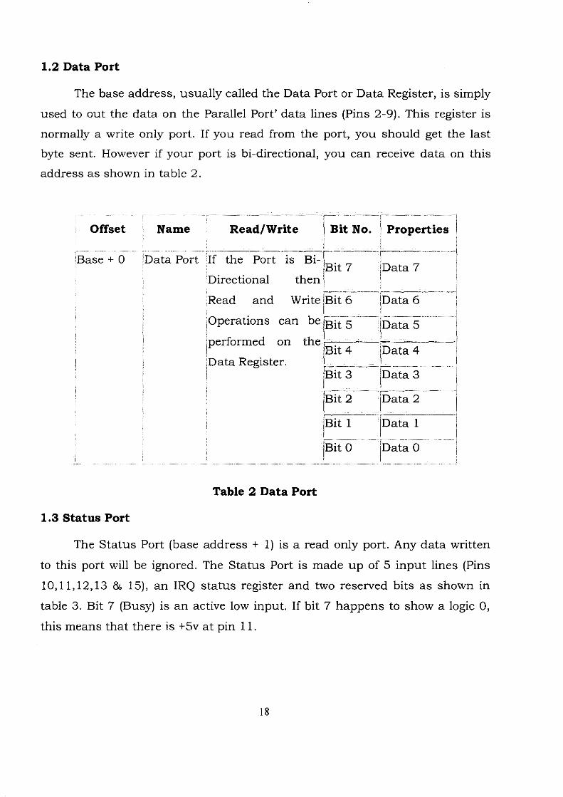
1.2 Data Port
The base address, usually called the Data Port or Data Register, is simply
used to out the data on the Parallel Port’ data lines (Pins 2-9). This register is
normally a write only port. If you read from the port, you should get the last
byte sent. However if your port is bi-directional, you can receive data on this
address as shown in table 2.
Offset
Base + 0
1.3 Status Port
Name Read/Write
Data Port If the Port is Bi-
Directional then
Read and Write
|Operations can be
jperformed on the
]Data Register.
Bit No. I Properties
Table 2 Data Port
Bit 7 Data 7
Bit 6 Data 6
Bit 5 Data 5
Bit 4 Data 4
Bit 3 Data 3
Bit 2 Data 2
Bit 1 Data 1
Bit 0 Data 0
The Status Port (base address + 1) is a read only port. Any data written
to this port will be ignored. The Status Port is made up of 5 input lines (Pins
10,11,12,13 & 15), an IRQ status register and two reserved bits as shown in
table 3. Bit 7 (Busy) is an active low input. If bit 7 happens to show a logic 0,
this means that there is +5v at pin 11.
18

I Offset i Name i Read/Write P Bit No. {Properties ji I _ __ 1 I ! !
Base + 1 S tatus Port jRead Onlyj ; I [Bit..6 ..... ' ..1 !I 1 ! j........... .... - ^Status IBit 5 ; !! ' I______ :____B its |
: (Bit 4 ' |; ! j i s !
. IB it 3I [Mir. 2 IRQ (Not)
! jBit 1 Reserved i? ■ ' i s
I [Bit 0 Reserved I
Table 3 Status Port
1.4 Control Port
The Control Port (base address + 2) is tended as a write only port shown in table 4. There are four control bits, all of which are inverted except Bit 2. If someone enables Bit 5, the data port behaves as input port.
Offset i Name 1 Read/Write j Bit No. j Properties
Base + 2 jControl jRead/Write [Bit 7 jUnusedj \ i . . . . . . . .-i. .... ........Port [Bit 6 jUnused j
Bit 5 [Enable Bi-'j[Directional Port I
Bit 4 Enable IRQ ~ j(Bit 3 Bit 2 (Control BitsBit 1 iBit 0
Table 4 Control Port
19

Datasheet of Counter
APPENDIX-B
nn u a d d i s CD4020BMS, CD4024BMS CD4040BMSS E M I C O N D U C T O R
CMOS Ripple-Carry Binary October 1996 Counter/Dividers
Features• High Voltage Types (20V Rating)• Medium Speed Operation• Fully Static Operation• Buffered Inputs and Outputs• 100% Tested for Quiescent Current at 20V• Standardized Symmetrical Output Characteristics• Common Reset• 5V, 10V and 15V Parametric Ratings• Maximum Input Current oMjia at 18V Over Full Pack-
age-Temperature Range;- 100nA at 18V and 25°C
• Noise Margin (Over Full Package Temperature Range):- 1V atVDD = 5V- 2V atVDD = 10V- 2.5VatVDD = 15V
• Meets All Requirements of JEDEC Tentative Standard No. 1SB, "Standard Specifications For Description Of 'B’ Series CMOS Devices”
Applications• Control Counters » Timers► Frequency Dividers » Tlme-Delay Circuits
DescriptionCD4020BMS - 14 Stage CD4024BMS - 7 Stage
CD4040BMS - 12 Stage
CD4020BMS, CD4024BMS. and CD4C40BMS are ripple- cany binary counters. All counter stages are master-slave flip-flops. The state of a counter advances one couni on the negative transition of each input pulse; a high level on the RESET line resets the counter to its all zeros slate. Schmitt trigger action on the inpul-pulse line permits unlimited rise and fall times. All inputs and outputs are buffered.
The CD4020BMS, CD4024BMS and (he CD4040BMS is supplied in Ihese 14 lead outline packages:
CD4020B CD4024B CD4040B
Braze Seal DiP H4W H4Q H4X
Frit Sea) DIP HI F H1B H1F
Ceramic Flatpack H6W H3W H6W
PinoutsCD4020BMSTo p vi ew
012 [7-------- u --------
U|V0D
o n [7 i ^ o t i
0 1 4 ^ m | oio
06 [7 j3]Q«
05 [5
07 (T n ] RESET
Q4 Q 7o|e
v s s jT 3 ® ’
C04Q24BMSTOP VIEW
Ve t l i 3 VDD
RESET [7 iH NC07 [7 Q1
q* [ 7
Q5 [7 ! 3 nc
fl] 03
vss ^ T J nc
NC = NO CONNECTION
CD4040BMSTOP VIEW
< a « [7------- ----------
is] VDD
06 [7 i j j o i i
os [7 m ] qio
Q? \T 13]Q8
04 E 12] 09
03 E n j r
0 2 [T W]9
v s s [T 9 ]« 1
Specification of Counter
2 0

Specifications CD4020BMS, CD4024BMS, CD4040BMS
TABLE 8. BURN-IN AND IRRADIATION TEST CONNECTIONS (Continued)
FUNCTION OPEN GROUND VDD 9V ± -0.5V
OSCILLATOR
50kHz 25kHz
Stabc Burn-In 2 Note 1
3 - 6 . 8 - 1 3 7 1,2 . 14
Dynamic Burn- In Note 1
8. 10.13 2 .7 14 3 - 6 . 9 . . 1 1 , 12 1
Irradiation Note 2
3 - 6 . 8 - 1 3 7 1 ,2 .1 4
PARTNUMBER CD4040BMS
Static Burn-In 1 Note 1
1 - 7 , 9 , 1 2 - 1 5 8. 10, 11 16
Static Burn-In 2 Note 1
1 - 7 , 9 , 1 2 - 1 6 8 10, 11. 16
Dynamic Burn- in Note 1
8. 11 16 1 - 7 , 9 , 1 2 - 1 5 10
Irradiation Note 2
1 -7 , 9 ,1 2 -15 8 10, 11 ,16
NOTE:1 Each pm exceptVDD and GND will have a series resistor of 10 K ± 5%, VDO = 18V±0 .5V
2 Each pin except VDO and GND wifi have a series resistor 0f47K±5%; Group E, Subgroup 2, sample size is A dice/wafer, 0 failures. VDD = 10V ± 0.5V
Functional Diagrams
INPUTPULSES
11RESET
VDD ♦ 16
14 STAGE RIPPLE
COUNTER
T*vss
01 \
' Q4 05 Q6 Q7 OS Q9 010 q iiOt2 Q13 Q14 y
Q6
INPUTPULSES
11
RESET
VDD416
12 STAGE RIPPLE
COUNTER
T «VSS
_9_ Q1 ^ _7_02 6 03
^ 0 4
_2_Q«i - Q7J3 Q$_12 Q9 _14 Q10 _15 Q11 _1_Q12 y
5oha
s
CD402OBMS CD4024BMS CD4040BMS
Functional Diagram of Counter

CD4020BMS, CD4024BMS, CD4040BMS
Logic Diagrams
K . FF1 FF2
I-------------------------- i ~ !
01 Q1
• in puts p r o tec ted8Y COSMOS PROTECTION NETWORK
02 Q2 03 <913
FF3-FF13
04 Q13
014 Q14
014 Q14
y y y y<314
FIGURE 1. LOGIC DIAGRAM FOR CD402QBMS
Q2 Q3 qe
FIGURE 2. LOGIC DIAGRAM FOR CD4Q24BMS
VDD
01 Q1
FF1
01 Q1 R Q1
I
02 Q2
FF2
02 02
1 *i —i 1 r — f !
* * VA- * 1t IINPUTS PROTECTEDBYC0S/M0SPR0TECT10NNETWORK
03 Q11
®3 511
FF3- FF11
07 Q12
FF12
07 Q12
Q2 03 011Y
Q12
FIGURE 3. LOGIC DIAGRAM FOR CD40408MS
Logic Diagram of counter
2 2


![Two-pulse magnetic field-free switching scheme for perpendicular … · 2020. 2. 17. · element of magnetoresistive random access memory (MRAM) [2]. Their parallel and anti-parallel](https://static.fdocuments.in/doc/165x107/60bd697e7b4aac1aae47c326/two-pulse-magnetic-field-free-switching-scheme-for-perpendicular-2020-2-17.jpg)