
Pulse Density Modulation Control using Space Vector...
7
Pulse Density Modulation Control using Space Vector Modulation for a Single-phase to Three-phase Indirect Matrix Converter Yuki Nakata Energy and Environmental Science Nagaoka University of Technology Nagaoaka, Japan [email protected] Jun-ichi Itoh Electrical Engineering Nagaoka University of Technology Nagaoaka, Japan [email protected] Abstract—This paper discusses pulse density modulation (PDM) control methods for a single-phase to three-phase matrix converter for high-frequency applications such as the grid interface converter for a wireless power transfer system and high-frequency transformer link system. The input frequency for this converter is assumed as several hundred kHz, and at the same time outputting a commercial grid frequency, i.e. 50 Hz or 60 Hz. The proposed circuit achieves high efficiency by implementing zero voltage switching from a PDM control method. In this paper, the PDM that is based on space vector modulation (SVM) is proposed in order to improve the output waveform. Simulation and experimental results are demonstrated and discussed. From the results, the total harmonic distortion (THD) of the output voltage, which is controlled by the PDM using delta-sigma conversion, and the proposed PDM based on SVM are 5.96% and 2.15%, respectively. Furthermore, the proposed circuit achieves maximum efficiency up to 97.3% with the proposed PDM based on SVM. From the results, the validity of the PDM control based on SVM has been confirmed. I. INTRODUCTION In recent year, wireless power transfer systems have been actively researched [1-3]. There are two types of wireless power systems known as the electromagnetic induction and magnetic resonant coupling. In the electromagnetic induction type, the frequency of the coil for the transmission is low, and it can transmit high-capacity power with relative ease. However, when the coupling is reduced it will result the transmitting efficiency decreases with increasing in the transmission distance. As a result, a large coupling of the transmission coils is necessary in order to improve the transmitting efficiency. Likewise, the transmitting distance needs to become shorter. On the other hand, the efficiency of the electromagnetic resonant coupling type is over 90% at the intermediate distance which is approximately 1 m [4]. In the wireless power transfer system, the frequency of the generated voltage at the receiving coil is from tens of kHz to several MHz, which is identical to the power source frequency. Accordingly, in order to connect this system to a load, an interface converter which converts the received power into a controlled output power is required. The characteristic of this interface converter must has a high input frequency from several hundred kHz and able to deliver a low output frequency (50 Hz or 60 Hz) suitable for commercial power grid. That is, an AC-to-AC converter is generally clarified as the interface converter for this system. Matrix converter (MC) has been attracted attentions as the AC interface converter for the wireless system, because it delivers advantages in terms of size reduction and energy saving [5-7]. However, the implementation of MC in the high-frequency power source has not been reported. In addition, the AC-to-AC converter for the high- frequency application is necessary in other case. For example, the MC for high-frequency application can be applied to trans-linked converter, whose secondary side is connected to commercial grid. In downsizing the converter, the transformer for high-frequency link size is a major bottleneck [8]. Therefore, the size of the transformer can be small by higher frequency converter using high-speed switching devices such as SiC and GaN. This paper discusses the single-phase to three-phase matrix converter for high frequency operation. There are two type topologies for the matrix converter, so called indirect matrix converter (IMC) and conventional matrix converter (CMC). In this paper, the indirect matrix converter is used due to the simple control. The authors have previously proposed a Pulse density modulation (PDM) [9-11] control method for the high-frequency power source [12-14]. The proposed control method applies Zero Voltage Switching (ZVS) to reduce the switching loss. The PDM signals can be obtained from delta-sigma conversion. However, in the delta-sigma conversion, the inverse voltage pulses and clamp phenomena will occur in the output voltage waveform of the
Transcript of Pulse Density Modulation Control using Space Vector...
Pulse Density Modulation Control using Space Vector Modulation for a Single-phase to Three-phase Indirect
Matrix Converter
Yuki Nakata Energy and Environmental Science Nagaoka University of Technology
Nagaoaka, Japan [email protected]
Jun-ichi Itoh Electrical Engineering
Nagaoka University of Technology Nagaoaka, Japan
Abstract—This paper discusses pulse density modulation (PDM) control methods for a single-phase to three-phase matrix converter for high-frequency applications such as the grid interface converter for a wireless power transfer system and high-frequency transformer link system. The input frequency for this converter is assumed as several hundred kHz, and at the same time outputting a commercial grid frequency, i.e. 50 Hz or 60 Hz. The proposed circuit achieves high efficiency by implementing zero voltage switching from a PDM control method. In this paper, the PDM that is based on space vector modulation (SVM) is proposed in order to improve the output waveform. Simulation and experimental results are demonstrated and discussed. From the results, the total harmonic distortion (THD) of the output voltage, which is controlled by the PDM using delta-sigma conversion, and the proposed PDM based on SVM are 5.96% and 2.15%, respectively. Furthermore, the proposed circuit achieves maximum efficiency up to 97.3% with the proposed PDM based on SVM. From the results, the validity of the PDM control based on SVM has been confirmed.
I. INTRODUCTION In recent year, wireless power transfer systems have been
actively researched [1-3]. There are two types of wireless power systems known as the electromagnetic induction and magnetic resonant coupling. In the electromagnetic induction type, the frequency of the coil for the transmission is low, and it can transmit high-capacity power with relative ease. However, when the coupling is reduced it will result the transmitting efficiency decreases with increasing in the transmission distance. As a result, a large coupling of the transmission coils is necessary in order to improve the transmitting efficiency. Likewise, the transmitting distance needs to become shorter. On the other hand, the efficiency of the electromagnetic resonant coupling type is over 90% at the intermediate distance which is approximately 1 m [4].
In the wireless power transfer system, the frequency of the generated voltage at the receiving coil is from tens of
kHz to several MHz, which is identical to the power source frequency. Accordingly, in order to connect this system to a load, an interface converter which converts the received power into a controlled output power is required. The characteristic of this interface converter must has a high input frequency from several hundred kHz and able to deliver a low output frequency (50 Hz or 60 Hz) suitable for commercial power grid. That is, an AC-to-AC converter is generally clarified as the interface converter for this system.
Matrix converter (MC) has been attracted attentions as the AC interface converter for the wireless system, because it delivers advantages in terms of size reduction and energy saving [5-7]. However, the implementation of MC in the high-frequency power source has not been reported.
In addition, the AC-to-AC converter for the high-frequency application is necessary in other case. For example, the MC for high-frequency application can be applied to trans-linked converter, whose secondary side is connected to commercial grid. In downsizing the converter, the transformer for high-frequency link size is a major bottleneck [8]. Therefore, the size of the transformer can be small by higher frequency converter using high-speed switching devices such as SiC and GaN.
This paper discusses the single-phase to three-phase matrix converter for high frequency operation. There are two type topologies for the matrix converter, so called indirect matrix converter (IMC) and conventional matrix converter (CMC). In this paper, the indirect matrix converter is used due to the simple control. The authors have previously proposed a Pulse density modulation (PDM) [9-11] control method for the high-frequency power source [12-14]. The proposed control method applies Zero Voltage Switching (ZVS) to reduce the switching loss. The PDM signals can be obtained from delta-sigma conversion. However, in the delta-sigma conversion, the inverse voltage pulses and clamp phenomena will occur in the output voltage waveform of the

Figure 1. Single-phase to three-phase indirect matrix converter.
Figure 2. PDM control block diagram using delta-sigma conversion.
IMC. The clamp phenomenon will occur, when the phase between the output voltage and current becomes larger instantaneously.
In this paper, the PDM control based on Space vector modulation (SVM) is proposed in order to improve the quality of output waveform. The proposed method generates switching patterns based on SVM in order to minimize the phase error between output voltage and current. Therefore, there are no clamp phenomena will occur on the output voltage waveform. This paper compares and investigates two PDM control methods, which are based on the delta-sigma conversion and SVM. Firstly, the configurations of the proposed circuit are introduced. Secondly, the PDM control strategy using the delta-sigma conversion and the improved PDM method based on the SVM are discussed. Finally, the validity of the proposed method is confirmed in the simulation and experimental results.
II. CIRUIT CONFIGURATION Fig. 1 shows circuit configuration of the proposed single-
phase to three-phase IMC. This circuit is constructed from a diode rectifier as an input interface and a three-phase inverter for the rear side. Since this converter does not required electrolytic capacitors in the DC link, the lifetime is longer and the size is more compact than the conventional system, which is constructed by a PWM rectifier, electrolytic capacitors and a three-phase PWM inverter.
In addition, a low pass filter is connected to the input side in order to smooth the input current and match the impedance of the circuit and the source. The detail of input-filter design method is explained in chapter IV.
Note that, in the experimental circuit, a snubber circuit is connected to the DC link as a protection circuit. It is constructed by a diode, a small capacitor and a resistor.
III. CONTROL STRATEGY
A. PDM Control using Delta-sigma Conversion A PDM control method is applied to the proposed system
in order to reduce the switching loss of the inverter side. PDM controls the density and the plus/minus of the constant-width pulse, and then these pulse signals are used as the output unit.
Fig. 2 shows the control block diagram of the proposed circuit. The PDM signals used for the switching can be obtained by converting the delta-sigma command (vu*, vv*, vw*) value from each phase. In general, delta-sigma conversion is used for analog-digital conversion. These PDM signals are used to turn on/off the inverter arm of the proposed circuit.
Additionally, the zero cross points exist with respects to the frequency since the input voltage is a sinusoidal waveform. The turn-on and off of the switching are implemented at every zero cross points of the input voltage in ZVS. The loss from the switching devices at the inverter can reduce drastically because the switching loss can be
decreased nearly to zero by the implementation of the ZVS operation.
However, there are problems in this method, due to the inverse voltage pulses and clamp phenomena that are constant voltage areas will occur. Delta-sigma conversion generates the inverse voltage pulses in order to cancel the quantization error. In the clamped parts, switching loss increases because the ZVS cannot be achieved. The clamp phenomenon occurs because when the phase between the voltage and current becomes larger than 30 degrees, the DC link current flows backward to the power source in the inverter side. As a result, the DC link voltage is equaled to the snubber capacitor voltage. In order to resolve this problem, the PDM based SVM is proposed to apply for the generation of PDM patterns. The detail of this method is explained in the next section.
B. PDM Control based on Space Vector Modulation In the proposed PDM based SVM, the phase error
between the voltage and current does not occur rapidly, because the SVM controller can select the switching pattern, which results the phase change on the voltage becomes smaller. Hence, the link current does not flow backward and the snubber diode does not turn on. Therefore, the clamp phenomenon does not occur. The switching loss of the device decreases applying this method, because the clamp phenomenon does not occur.
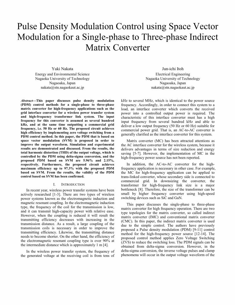
Fig. 3 shows the PDM signal generation block based on the SVM. The switching signals generated from the SVM is the input to the D flip-flop (D-FF), and +/- detection signal from the input voltage is used to detect the zero cross points of input voltage, this signal is an input to the CLK. The output of the D-FF, “Q” is synchronized at the edge of +/- signal, which is the zero cross point of input voltage. As a result, the switching signals generated by SVM are quantized
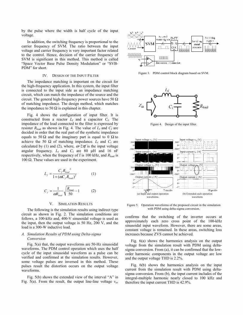
Figure 3. PDM control block diagram based on SVM.
Figure 4. Design of the input filter.
0-500
500
0
-1
1
0-500
500
0
-1
1
0-500
500
0
-1
1
0-500
500
0
-1
1
Input voltage vin
Input current iin
[V]
[V]
[A]
[A]
Output voltage vuv
Output current iu
s/divms/div(a) Input and output operation
waveforms.(b) Extended each operation
waveform.
A
Input voltage vin
Input current iin
[V]
[V]
[A]
[A]
Output voltage vuv
Output current iu
Figure 5. Operation waveforms of the proposed circuit in the simulation with PDM using delta-sigma conversion.
by the pulse where the width is half cycle of the input voltage.
In addition, the switching frequency is proportional to the carrier frequency of SVM. The ratio between the input voltage and carrier frequency is very important factor related to the control. Hence, decision of the carrier frequency of SVM is significant in this method. This method is called “Space Vector Base Pulse Density Modulation” or “SVB-PDM” for short.
IV. DESIGN OF THE INPUT FILTER The impedance matching is important on the circuit for
the high-frequency application. In this system, the input filter is connected to the input side as an impedance matching circuit, which can match the impedance of the source and the circuit. The general high-frequency power sources have 50 Ω of matching impedance. The design method, which matches the impedance to 50 Ω is explained in this chapter.
Fig. 4 shows the configuration of input filter. It is constructed from a reactor Lf and a capacitor Cf. The impedance of the load connected to the filter is expressed by resister Rload as shown in Fig. 4. The value of Lf and Cf are decided in order that the real part of the synthetic impedance equals to 50 Ω and the imaginary part is equal to 0 Ω to achieve the 50 Ω of matching impedance. Lf and Cf are calculated by (1) and (2), where, ω=2πf is the input voltage angular frequency. Lf and Cf are 80 μH and 16 nF respectively, when the frequency of f is 100 kHz, and Rload is 100 Ω. These values are used in the experiment.
2
2
)(1 loadf
loadff RC
RCL
ω+= (1)
150
1 −= load
loadf
RR
Cω
(2)
V. SIMILATION RESULTS The following is the simulation results using indirect type
circuit as shown in Fig. 2. The simulation conditions are follows, a 100-kHz and, 400-V sinusoidal voltage is used as the input, then the output voltage is 50 Hz, 200 V, and the load is a 300-W inductive load.
A. Simulation Results of PDM using Delta-sigma Conversion Fig. 5(a) that, the output waveforms are 50-Hz sinusoidal
waveforms. The PDM control operation which uses the half cycle of the input sinusoidal waveform as a pulse can be verified and confirmed at the simulation results. However, some voltage pulses are inversed in this method. These pulses result the distortion occurs on the output voltage waveforms.
Fig. 5(b) shows the extended view of the interval “A” in Fig. 5(a). From the result, the output line-line voltage vuv
confirms that the switching of the inverter occurs at approximately each zero cross point of the 100-kHz sinusoidal input waveform. However, there are some areas, constant voltage is remained. In these areas, switching loss increases because ZVS cannot be achieved.
Fig. 6(a) shows the harmonics analysis on the output voltage from the simulation result with PDM using delta-sigma conversion. From (a), it can be confirmed that the low-order harmonic components in the output voltage are low and the output voltage THD is 2.2%.
Fig. 6(b) shows the harmonics analysis on the input current from the simulation result with PDM using delta-sigma conversion. From (b), the input current includes of the integral-multiple harmonic nearly closed to 100 kHz and therefore the input current THD is 42.9%.
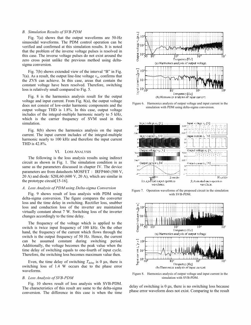
Figure 6. Harmonics analysis of output voltage and input current in the
simulation with PDM using delta-sigma conversion.
Figure 7. Operation waveforms of the proposed circuit in the simulation with SVB-PDM.
Figure 8. Harmonics analysis of output voltage and input current in the simulation with SVB-PDM.
B. Simulation Results of SVB-PDM Fig. 7(a) shows that the output waveforms are 50-Hz
sinusoidal waveforms. The PDM control operation can be verified and confirmed at this simulation results. It is noted that the problem of the inverse voltage pulses is resolved in this case. The inverse voltage pulses do not exist around the zero cross point unlike the previous method using delta-sigma conversion.
Fig. 7(b) shows extended view of the interval “B” in Fig. 7(a). As a result, the output line-line voltage vuv confirms that the ZVS can achieve. In this case, areas that contain the constant voltage have been resolved. Therefore, switching loss is relatively small compared to Fig. 5.
Fig. 8 is the harmonics analysis result for the output voltage and input current. From Fig. 8(a), the output voltage does not consist of low-order harmonic components and the output voltage THD is 1.8%. In this case, output voltage includes of the integral-multiple harmonic nearly to 5 kHz, which is the carrier frequency of SVM used in this simulation.
Fig. 8(b) shows the harmonics analysis on the input current. The input current includes of the integral-multiple harmonic nearly to 100 kHz and therefore the input current THD is 42.8%.
VI. LOSS ANALYSIS The following is the loss analysis results using indirect
circuit as shown in Fig. 1. The simulation condition is as same as the parameters discussed in chapter IV. The device parameters are from datasheets MOSFET: IRFP460 (500 V, 20 A) and diode: S20L60 (600 V, 20 A), which are similar in the prototype circuit[15-16].
A. Loss Analysis of PDM using Delta-sigma Conversion Fig. 9 shows result of loss analysis with PDM using
delta-sigma conversion. The figure compares the converter loss and the time delay in switching. Rectifier loss, snubber loss and conduction loss of the inverter are maintained virtually constant about 7 W. Switching loss of the inverter changes accordingly to the time delay.
The frequency of the voltage which is applied to the switch is twice input frequency of 100 kHz. On the other hand, the frequency of the current which flows through the switch is the output frequency of 50 Hz. Hence, the current can be assumed constant during switching period. Additionally, the voltage becomes the peak value when the time delay of switching equals to one-fourth of input cycle. Therefore, the switching loss becomes maximum value then.
Even, the time delay of switching Tdelay is 0 μs, there is switching loss of 1.4 W occurs due to the phase error waveforms.
B. Loss Analysis of SVB-PDM Fig. 10 shows result of loss analysis with SVB-PDM.
The characteristics of this result are same to the delta-sigma conversion. The difference in this case is when the time
delay of switching is 0 μs, there is no switching loss because phase error waveform does not exist. Comparing to the result
0
2
4
6
8
10
12
14
16
18
0 0.5 1 1.5 2 2.5 3 3.5 4 4.5 5
switching
conduction
Snubber loss
Rectifier loss
Figure 9. Converter losses vs delay time of switching with PDM using
delta-sigma conversion.
0
2
4
6
8
10
12
14
16
18
0 0.5 1 1.5 2 2.5 3 3.5 4 4.5 5
switching
conduction
Snubber loss
Rectifier loss
0.0
Switching loss of inverter
Conduction loss of inverter
Snubber loss
Rectifier loss
0.5 1.0 1.5 2.0 2.5 3.0 3.5 4.0 4.5 5.0
18
161412
10
86420
Time delay of switching Tdelay [ s] Figure 10. Converter losses vs delay time of switching with SVB-PDM.
TABLE I. EXPERIMENTAL PARAMETERS.
Parameter Value Input voltage 200 [V] Input voltage 100 [kHz]
Output line-to-line voltage 100 [V] Output frequency 50 [Hz]
Load Rload 100 [Ω] Lload 10 [mH]
Figure 11. Operation waveforms of the proposed circuit in the experiment
with PDM using delta-sigma conversion.
from Fig. 9, the loss is reduced by approximately 18%. Therefore, the size of snuber circuit can be smaller than that with the PDM using delta-sigma conversion.
VII. EXPERIMENTAL RESULTS In order to demonstrate the validity of the proposed
circuit, a prototype circuit has been built and tested. The single-phase to three-phase IMC was tested in the experiment with the two proposed PDM control methods. A high-frequency power source, where the matching impedance is 50 Ω is used as the input circuit initially to confirm the basic principle of the two proposed control methods. Table 1 shows the experimental conditions.
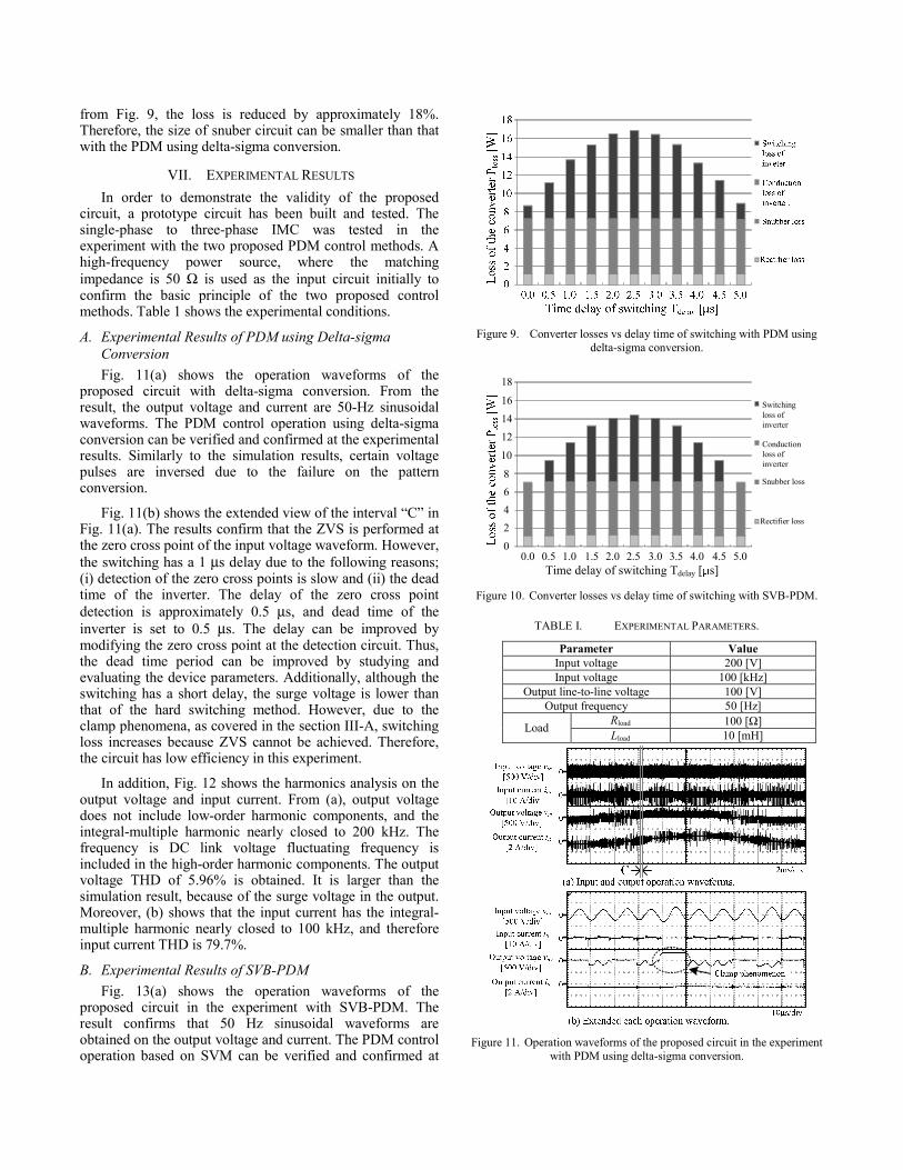
A. Experimental Results of PDM using Delta-sigma Conversion Fig. 11(a) shows the operation waveforms of the
proposed circuit with delta-sigma conversion. From the result, the output voltage and current are 50-Hz sinusoidal waveforms. The PDM control operation using delta-sigma conversion can be verified and confirmed at the experimental results. Similarly to the simulation results, certain voltage pulses are inversed due to the failure on the pattern conversion.
Fig. 11(b) shows the extended view of the interval “C” in Fig. 11(a). The results confirm that the ZVS is performed at the zero cross point of the input voltage waveform. However, the switching has a 1 μs delay due to the following reasons; (i) detection of the zero cross points is slow and (ii) the dead time of the inverter. The delay of the zero cross point detection is approximately 0.5 μs, and dead time of the inverter is set to 0.5 μs. The delay can be improved by modifying the zero cross point at the detection circuit. Thus, the dead time period can be improved by studying and evaluating the device parameters. Additionally, although the switching has a short delay, the surge voltage is lower than that of the hard switching method. However, due to the clamp phenomena, as covered in the section III-A, switching loss increases because ZVS cannot be achieved. Therefore, the circuit has low efficiency in this experiment.
In addition, Fig. 12 shows the harmonics analysis on the output voltage and input current. From (a), output voltage does not include low-order harmonic components, and the integral-multiple harmonic nearly closed to 200 kHz. The frequency is DC link voltage fluctuating frequency is included in the high-order harmonic components. The output voltage THD of 5.96% is obtained. It is larger than the simulation result, because of the surge voltage in the output. Moreover, (b) shows that the input current has the integral-multiple harmonic nearly closed to 100 kHz, and therefore input current THD is 79.7%.
B. Experimental Results of SVB-PDM Fig. 13(a) shows the operation waveforms of the
proposed circuit in the experiment with SVB-PDM. The result confirms that 50 Hz sinusoidal waveforms are obtained on the output voltage and current. The PDM control operation based on SVM can be verified and confirmed at
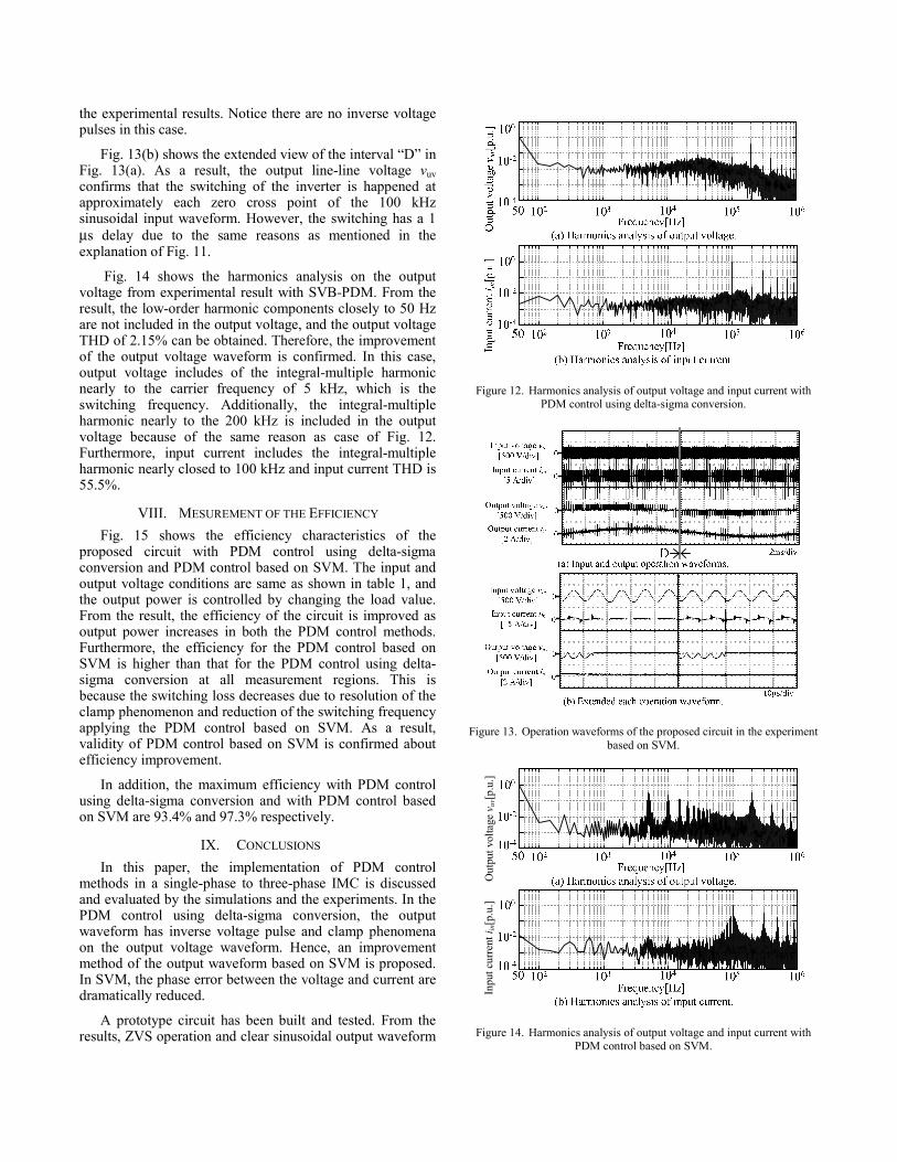
Figure 12. Harmonics analysis of output voltage and input current with PDM control using delta-sigma conversion.
Figure 13. Operation waveforms of the proposed circuit in the experiment based on SVM.
Out
put v
olta
ge v
uv[p
.u.]
Inpu
t cur
rent
i in[
p.u.
]
Figure 14. Harmonics analysis of output voltage and input current with PDM control based on SVM.
the experimental results. Notice there are no inverse voltage pulses in this case.
Fig. 13(b) shows the extended view of the interval “D” in Fig. 13(a). As a result, the output line-line voltage vuv confirms that the switching of the inverter is happened at approximately each zero cross point of the 100 kHz sinusoidal input waveform. However, the switching has a 1 μs delay due to the same reasons as mentioned in the explanation of Fig. 11.
Fig. 14 shows the harmonics analysis on the output voltage from experimental result with SVB-PDM. From the result, the low-order harmonic components closely to 50 Hz are not included in the output voltage, and the output voltage THD of 2.15% can be obtained. Therefore, the improvement of the output voltage waveform is confirmed. In this case, output voltage includes of the integral-multiple harmonic nearly to the carrier frequency of 5 kHz, which is the switching frequency. Additionally, the integral-multiple harmonic nearly to the 200 kHz is included in the output voltage because of the same reason as case of Fig. 12. Furthermore, input current includes the integral-multiple harmonic nearly closed to 100 kHz and input current THD is 55.5%.
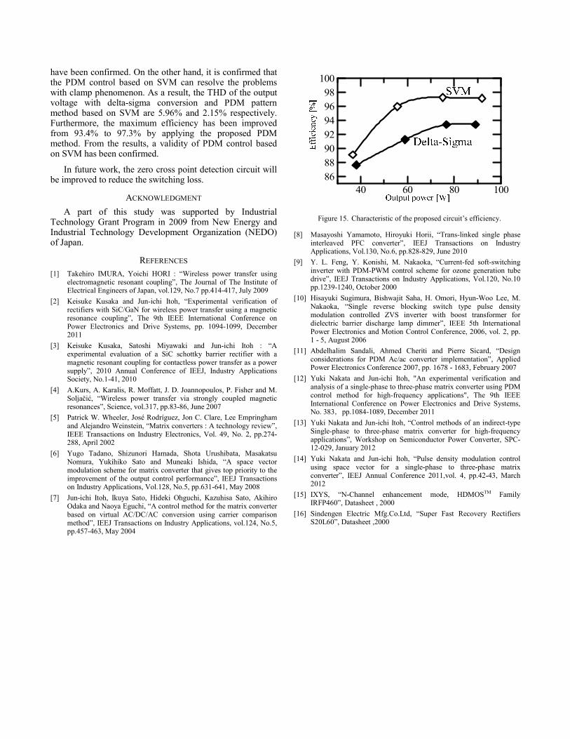
VIII. MESUREMENT OF THE EFFICIENCY Fig. 15 shows the efficiency characteristics of the
proposed circuit with PDM control using delta-sigma conversion and PDM control based on SVM. The input and output voltage conditions are same as shown in table 1, and the output power is controlled by changing the load value. From the result, the efficiency of the circuit is improved as output power increases in both the PDM control methods. Furthermore, the efficiency for the PDM control based on SVM is higher than that for the PDM control using delta-sigma conversion at all measurement regions. This is because the switching loss decreases due to resolution of the clamp phenomenon and reduction of the switching frequency applying the PDM control based on SVM. As a result, validity of PDM control based on SVM is confirmed about efficiency improvement.
In addition, the maximum efficiency with PDM control using delta-sigma conversion and with PDM control based on SVM are 93.4% and 97.3% respectively.
IX. CONCLUSIONS In this paper, the implementation of PDM control
methods in a single-phase to three-phase IMC is discussed and evaluated by the simulations and the experiments. In the PDM control using delta-sigma conversion, the output waveform has inverse voltage pulse and clamp phenomena on the output voltage waveform. Hence, an improvement method of the output waveform based on SVM is proposed. In SVM, the phase error between the voltage and current are dramatically reduced.
A prototype circuit has been built and tested. From the results, ZVS operation and clear sinusoidal output waveform
40 60 80 10086889092949698
100
Figure 15. Characteristic of the proposed circuit’s efficiency.
have been confirmed. On the other hand, it is confirmed that the PDM control based on SVM can resolve the problems with clamp phenomenon. As a result, the THD of the output voltage with delta-sigma conversion and PDM pattern method based on SVM are 5.96% and 2.15% respectively. Furthermore, the maximum efficiency has been improved from 93.4% to 97.3% by applying the proposed PDM method. From the results, a validity of PDM control based on SVM has been confirmed.
In future work, the zero cross point detection circuit will be improved to reduce the switching loss.
ACKNOWLEDGMENT A part of this study was supported by Industrial
Technology Grant Program in 2009 from New Energy and Industrial Technology Development Organization (NEDO) of Japan.
REFERENCES [1] Takehiro IMURA, Yoichi HORI : “Wireless power transfer using
electromagnetic resonant coupling”, The Journal of The Institute of Electrical Engineers of Japan, vol.129, No.7 pp.414-417, July 2009
[2] Keisuke Kusaka and Jun-ichi Itoh, “Experimental verification of rectifiers with SiC/GaN for wireless power transfer using a magnetic resonance coupling”, The 9th IEEE International Conference on Power Electronics and Drive Systems, pp. 1094-1099, December 2011
[3] Keisuke Kusaka, Satoshi Miyawaki and Jun-ichi Itoh : “A experimental evaluation of a SiC schottky barrier rectifier with a magnetic resonant coupling for contactless power transfer as a power supply”, 2010 Annual Conference of IEEJ, Industry Applications Society, No.1-41, 2010
[4] A.Kurs, A. Karalis, R. Moffatt, J. D. Joannopoulos, P. Fisher and M. Soljačić, “Wireless power transfer via strongly coupled magnetic resonances”, Science, vol.317, pp.83-86, June 2007
[5] Patrick W. Wheeler, José Rodríguez, Jon C. Clare, Lee Empringham and Alejandro Weinstein, “Matrix converters : A technology review”, IEEE Transactions on Industry Electronics, Vol. 49, No. 2, pp.274-288, April 2002
[6] Yugo Tadano, Shizunori Hamada, Shota Urushibata, Masakatsu Nomura, Yukihiko Sato and Muneaki Ishida, “A space vector modulation scheme for matrix converter that gives top priority to the improvement of the output control performance”, IEEJ Transactions on Industry Applications, Vol.128, No.5, pp.631-641, May 2008
[7] Jun-ichi Itoh, Ikuya Sato, Hideki Ohguchi, Kazuhisa Sato, Akihiro Odaka and Naoya Eguchi, “A control method for the matrix converter based on virtual AC/DC/AC conversion using carrier comparison method”, IEEJ Transactions on Industry Applications, vol.124, No.5, pp.457-463, May 2004
[8] Masayoshi Yamamoto, Hiroyuki Horii, “Trans-linked single phase interleaved PFC converter”, IEEJ Transactions on Industry Applications, Vol.130, No.6, pp.828-829, June 2010
[9] Y. L. Feng, Y. Konishi, M. Nakaoka, “Current-fed soft-switching inverter with PDM-PWM control scheme for ozone generation tube drive”, IEEJ Transactions on Industry Applications, Vol.120, No.10 pp.1239-1240, October 2000
[10] Hisayuki Sugimura, Bishwajit Saha, H. Omori, Hyun-Woo Lee, M. Nakaoka, “Single reverse blocking switch type pulse density modulation controlled ZVS inverter with boost transformer for dielectric barrier discharge lamp dimmer”, IEEE 5th International Power Electronics and Motion Control Conference, 2006, vol. 2, pp. 1 - 5, August 2006
[11] Abdelhalim Sandali, Ahmed Cheriti and Pierre Sicard, “Design considerations for PDM Ac/ac converter implementation”, Applied Power Electronics Conference 2007, pp. 1678 - 1683, February 2007
[12] Yuki Nakata and Jun-ichi Itoh, "An experimental verification and analysis of a single-phase to three-phase matrix converter using PDM control method for high-frequency applications", The 9th IEEE International Conference on Power Electronics and Drive Systems, No. 383,pp.1084-1089, December 2011
[13] Yuki Nakata and Jun-ichi Itoh, “Control methods of an indirect-type Single-phase to three-phase matrix converter for high-frequency applications”, Workshop on Semiconductor Power Converter, SPC-12-029, January 2012
[14] Yuki Nakata and Jun-ichi Itoh, “Pulse density modulation control using space vector for a single-phase to three-phase matrix converter”, IEEJ Annual Conference 2011,vol. 4, pp.42-43, March 2012
[15] IXYS, “N-Channel enhancement mode, HDMOSTM Family IRFP460”, Datasheet , 2000
[16] Sindengen Electric Mfg.Co.Ltd, “Super Fast Recovery Rectifiers S20L60”, Datasheet ,2000