PT SERIES SIP Package - Datel · The PT series offers 3 watt of isolated output power in an 8 pin...
15
July 7, 2017 A.02 PT SERIES SIP Package 3 Watt Isolated DC-DC Converter FEATURES Industry Standard SIP 8 Package 3 Watts Isolated Output 2:1 Input Range Regulated Outputs Up to 86 % Efficiency -40°C to +85 operating temperature range Remote On/Off logic control Continuous Short Circuit Protection Under Voltage protection Meets 2004/108/EC Safety designed to meet UL60950-1, EN60950-1, and IEC60950-1 PRODUCT OVERVIEW The PT series offers 3 watt of isolated output power in an 8 pin SIP standard package. These converters have a 2:1 wide input voltage range of 4.5 to 9, 9 to 18, 18 to 36 or 36 to 75 Volts. This series of converters provides precise regulated output voltage ranging from 3.3 to 15 volts. The output voltage can be single or dual depending on the model. Other output voltages are also available and please contact DATEL if your application requires such modification. This series features high efficiency up to 86%; 1500Volts of DC of isolation and can operate over the ambient temperature range of –40°C to +70°C without derating. These modules are fully protected against output short circuit and under overvoltage conditions. APPLICATIONS: Distributed Power Architectures Mobile telecommunication Industrial applications Battery operated equipment AVAILABLE OPTIONS Customizable Input/ Output voltages UL/CSA60950-1, TUV per IEC/ EN60950-1, 2 nd Edition Contact DATEL for other series in SIP Package 4:1 Input Ranges Cost saving, lower / higher power, other output voltages etc. BLOCK DIAGRAM Page 1 of 15
Transcript of PT SERIES SIP Package - Datel · The PT series offers 3 watt of isolated output power in an 8 pin...

July 7, 2017 A.02
PT SERIES SIP Package 3 Watt Isolated DC-DC Converter
FEATURES Industry Standard SIP 8 Package 3 Watts Isolated Output 2:1 Input Range Regulated Outputs Up to 86 % Efficiency -40°C to +85 operating temperature range Remote On/Off logic control Continuous Short Circuit Protection Under Voltage protection Meets 2004/108/EC Safety designed to meet UL60950-1,
EN60950-1, and IEC60950-1
PRODUCT OVERVIEW The PT series offers 3 watt of isolated output power in an 8 pin SIP standard package. These converters have a 2:1 wide input voltage range of 4.5 to 9, 9 to 18, 18 to 36 or 36 to 75 Volts. This series of converters provides precise regulated output voltage ranging from 3.3 to 15 volts. The output voltage can be single or dual depending on the model. Other output voltages are also available and please contact DATEL if your application requires such modification.
This series features high efficiency up to 86%; 1500Volts of DC of isolation and can operate over the ambient temperature range of –40°C to +70°C without derating. These modules are fully protected against output short circuit and under overvoltage conditions.
APPLICATIONS: Distributed Power Architectures Mobile telecommunication Industrial applications Battery operated equipment
AVAILABLE OPTIONS Customizable Input/ Output voltages UL/CSA60950-1, TUV per IEC/ EN60950-1, 2nd Edition
Contact DATEL for other series in SIP Package 4:1 Input Ranges Cost saving, lower / higher power, other output voltages etc.
BLOCK DIAGRAM
Page 1 of 15

July 7, 2017 A.02
PT SERIES SIP Package 3 Watt Isolated DC-DC Converter
MODEL DESIGNATIONS
MODEL NUMBER INPUT VOLTAGE OUTPUT VOLTAGE OUTPUT CURRENT MAX EFFICIENCY % LOAD REGULATION LINE REGULATION PT5S3.3-0.7 4.5-9V 3.3VDC 700 mA 73 ± 0.5 % 0.5% PT5S5-0.6 4.5-9V 5.0 VDC 600 mA 78 ± 0.5 % 0.5%
PT5S12-0.25 4.5-9V 12 VDC 250 mA 81 ± 0.5 % 0.5% PT5S15-0.2 4.5-9V 15 VDC 200 mA 81 ± 0.5 % 0.5% PT5D5-.3 4.5-9V ±5.0 VDC ±300 mA 78 ± 1 % 0.5%
PT5D12-0.12 4.5-9V ±12 VDC ±125 mA 81 ± 1 % 0.5% PT5D15-0.1 4.5-9V ±15 VDC ±100 mA 81 ± 1 % 0.5%
PT12S3.3-0.7 9-18V 3.3VDC 700 mA 76 ± 0.5 % 0.5% PT12S5-0.6 9-18V 5.0 VDC 600 mA 81 ± 0.5 % 0.5%
PT12S12-0.25 9-18V 12 VDC 250 mA 83 ± 0.5 % 0.5% PT12S15-0.2 9-18V 15 VDC 200 mA 84 ± 0.5 % 0.5% PT12D05-0.3 9-18V ±5.0 VDC ±300 mA 82 ± 1 % 0.5%
PT12D12-0.12 9-18V ±12 VDC ±125 mA 83 ± 1 % 0.5% PT12D15-0.1 9-18V ±15 VDC ±100 mA 84 ± 1 % 0.5% PT24S3.3-0.7 18-36V 3.3VDC 700 mA 77 ± 0.5 % 0.5% PT24S05-0.6 18-36V 5.0 VDC 600 mA 81 ± 0.5 % 0.5%
PT24S12-0.25 18-36V 12 VDC 250 mA 84 ± 0.5 % 0.5% PT24S15-0.2 18-36V 15 VDC 200 mA 85 ± 0.5 % 0.5% PT24D05-0.3 18-36V ±5.0 VDC ±300 mA 80 ± 1 % 0.5%
PT24D12-0.12 18-36V ±12 VDC ±125 mA 84 ± 1 % 0.5% PT24D15-0.1 18-36V ±15 VDC ±100 mA 85 ± 1 % 0.5% PT48S3.3-0.7 36-75V 3.3VDC 700 mA 77 ± 0.5 % 0.5% PT48S05-0.6 36-75V 5.0 VDC 600 mA 81 ± 0.5 % 0.5%
PT48S12-0.25 36-75V 12 VDC 250 mA 86 ± 0.5 % 0.5% PT48S15-0.2 36-75V 15 VDC 200 mA 86 ± 0.5 % 0.5% PT48D05-0.3 36-75V ±5.0 VDC ±300 mA 81 ± 1 % 0.5%
PT48D12-0.12 36-75V ±12 VDC ±125 mA 86 ± 1 % 0.5% PT48D15-0.1 36-75V ±15 VDC ±100 mA 86 ± 1 % 0.5%
ABSOLUTE MAXIMUM RATINGS PARAMETER CONDITIONS MODEL Min. Typical Max. Units
Input Voltage
Continuous DC
5Vin 12Vin 24Vin
4.7 9
18
9 18 36 Volts
48Vin 36 75
Transient 100ms, DC
5Vin 12Vin 24Vin
15 25 50 Volts
48Vin 100
Operating Ambient Temperature Derating, Above 70℃ All -40 +85 ℃
Case Temperature All +100 ℃
Storage Temperature All -55 +125 ℃
Input / Output Isolation Voltage 1 minute All 1500 Volts
Page 2 of 15

July 7, 2017 A.02
PT SERIES SIP Package 3 Watt Isolated DC-DC Converter
INPUT CHARACTERISTICS Note: All specifications are typical at nominal input, full load at 25℃ unless otherwise noted PARAMETER CONDITIONS MODEL Min. Typical Max. Units
Operating Input Voltage
5Vin 12Vin 24Vin
4.5 9
18
5 12 24
9 18 36 Volts
48Vin 36 48 75
Input Under Voltage Lockout
Turn-On Voltage Threshold
5Vin 12Vin 24Vin
3.3 6.8 13
4.0 7.0
14.7
4.2 7.3
15.5
Volts 48Vin 26 28.5 31
Turn-Off Voltage Threshold
5Vin 12Vin 24Vin
3 5.8 12
3.5 6
13
3.9 6.3
14.5
Volts
48Vin 24 30 33
Lockout Hysteresis Voltage
5Vin 12Vin 24Vin
0.3 5 1
Volts
48Vin 2
Maximum Input Current
100% Load, Vin =4.5V 5Vin 890
mA 100% Load, Vin = 9V 12Vin 440 100% Load, Vin =18V 24Vin 220 100% Load, Vin =36V 48Vin 110
No-Load Input Current Vin =Nominal input
PT5S3.3-0.7 PT5S5-0.6
PT5S12-0.25 PT5S15-0.2 PT5D5-0.3
PT5D12-0.12 PT5D15-0.1
PT12S3.3-0.7 PT12S5-0.6
PT12S12-0.25 PT12S15-0.2 PT12D5-0.3
PT12D12-0.12 PT12D15-0.1 PT24S3.3-0.7
60 60 60 60 60 60 60 30 30 30 30 30 30 30 18
mA
PT24S5-0.6 18 PT24S12-0.18 18 PT24S15-0.2 PT24D5-0.3
18 18
PT24D12-0.12 18 PT24D15-0.1 18 PT48S3.3-0.7 9 PT48S5-0.6 9
PT48S12-0.25 9 PT48S15-0.2 PT48D5-0.3
9 9
PT48D12-0.12 9 PT48D15-0.1 9
Inrush Current (I2t) As per ETS300 132-2 All 0.01 A2s
Off Converter Input Current Shutdown input idle current All 1 mA
Input Reflected-Ripple Current P-P thru 12µH inductor, 5Hz to 20MHz All 30 mA
Page 3 of 15

July 7, 2017 A.02
PT SERIES SIP Package 3 Watt Isolated DC-DC Converter
OUTPUT CHARACTERISTIC PARAMETER CONDITIONS MODEL Min. Typical Max. Units
Output Voltage Set Point Vin =Nominal Vin , Io = Io_max, Tc=25℃
Vo=3.3 3.2505 3.3 3.3495
Volts
Vo=5.0 4.925 5 5.075 Vo=12 11.82 12 12.18 Vo=15
Vo=±5.0 14.775 4.925
15 5
15.225 5.075
Vo=±12 11.82 12 12.18 Vo=±15 14.775 15 15.225
Output Voltage Regulation
Line Regulation Vin =High line to Low line Full Load Single Dual
±0.5 ±0.5
% %
Load Regulation Io = Full Load to min. Load Single Dual
±0.5 ±1
% %
Cross Regulation Load cross variation 10%/100% Dual ±5 % Temperature Coefficient TC=-40℃ to + 85℃ ±0.03 %/℃ Output Voltage balance Vin =Nominal Vin , Io = Io_max, Tc=25℃ Dual ±1 %
Output Voltage Ripple and Noise
Peak-to-Peak Full Load, 20 MHz Single
75
mV Dual 75
Operating Output Current Range
Vo=3.3V 0
700
mA
Vo=5V 0 600
Vo=12V 0 250 Vo=15V Vo=±5V
0 0
200 ±300
Vo=±12V 0 ±125 Vo=±15V 0 ±100
Output DC Current-Limit Inception Output Voltage=90% VO, nominal 120 %
Maximum Output Capacitance Full load, Resistance
Vo=3.3V Vo=5V Vo=12V Vo=15V Vo=±5V
Vo=±12V Vo=±15V
700 600 250 200 300 125 100
µF
DYNAMIC CHARACTERISTICS PARAMETER CONDITIONS MODEL Min. Typical Max. Units
Output Voltage Current Transient
Step Change in Output Current 75% to 100% of Io_max di/dt=0.1A/us
All ±6 %
Setting Time (within 1% Vo nominal) All 500 µs
Turn-On Delay and Rise Time
Turn-On Delay Time, From On/Off Control Von/off to 10%Vo_set All 1 ms
Turn-On Delay Time, From Input Vin _min to 10%Vo_set All 1 ms
Output Voltage Rise Time 10% Vo_set to 90% Vo_set All 2.5 ms
Page 4 of 15

July 7, 2017 A.02
PT SERIES SIP Package 3 Watt Isolated DC-DC Converter
FEATURE CHARACTERISTICS PARAMETER CONDITIONS Device Min. Typical Max. Units
Efficiency 100% Load
Vin =5 Volts, Io = Io_max, Tc=25℃
PT5S3.3-0.7
73
%
PT5S5-0.6 78 PT5S12-0.25 81 PT5S15-0.2 81 PT5D5-0.3 78
PT5D12-0.12 81 PT5D15-0.1 81
Vin =12 Volts, Io = Io_max, Tc=25℃
PT12S3.3-0.7 76 PT12S5-0.6 81 PT12S12-0.25 83 PT12S15-0.2 84 PT12D5-0.3 82 PT12D12-0.12 83 PT12D15-0.1 84
Vin =24 Vdc, Io = Io_max, Tc=25℃
PT24S3.3-0.7 77 PT24S5-0.6 81
PT24S12-0.25 84 PT24S15-0.2 PT24D5-0.3
85 80
PT24D12-0.12 84 PT24D15-0.1 85
Vin =48 Vdc, Io = Io_max, Tc=25℃
PT48S3.3-0.7 77 PT48S5-0.6 81
PT48S12-0.25 86 PT48S15-0.2 PT48D5-0.3
86 81
PT48D12-0.12 86 PT48D15-0.1 86
ISOLATION CHARACTERISTICS Input to Output 1 minutes All 1500 Volts Isolation Resistance All 1000 MΩ Isolation Capacitance All 500 pF Switching Frequency 100 KHz On/Off Control, Positive Remote On/Off logic
Module On Von/off at Ion/off=0.1uA All 0 0 1.2 or Open Circuit
Volts
Module Off Von/off Pin All 5.5 +15 Volts On/Off Control, Option Under Voltage Control All 0.3 1 mA Module On
Open, High impedance 0 0.8 or open
circuit
Volts
Module Off V Remote On/Off Pin 4 +15 Volts Off Converter Input Current Shutdown input idle current 1 mA
MTBF Io =100%of Io_max;Ta=25℃ per MIL-HDBK-217F
All 2.5 M hours
Weight All 4.8 grams
Page 5 of 15
July 7, 2017 A.02
PT SERIES SIP Package 3 Watt Isolated DC-DC Converter
Operating Temperature Range The PT series converters operate over the wide ambient temperature range from -40℃ to +85℃. Derating for this series starts above the temperature of +70℃. For normal operation, the case temperature should not go over +100℃.
Remote On/Off The remote ON/OFF input feature of the converter allows external circuitry to turn the converter ON or OFF. Active-high Remote ON/OFF is available as standard. The converter is turned on if the Remote ON/OFF pin is high impedance or open circuit. Converter with added Suffix "U" to the model number are on with voltage below 0.8 volts at Remote ON/OFF pin and are off when the voltage at Remote ON/OFF pin is from 4 to 15 Volts. All other standard models turn the converter off when the signal at Remote ON/OFF is from 5.5 to 15Vdc. The signal level of the on/off pin is defined with respect to ground. If not using the on/off pin, leave the pin open (module will be on).
Over Current Protection All models have internal over current and continuous short circuit protection. The unit operates normally once the fault condition is removed. At the point of current limit inception, the converter will go into hiccup mode protection.
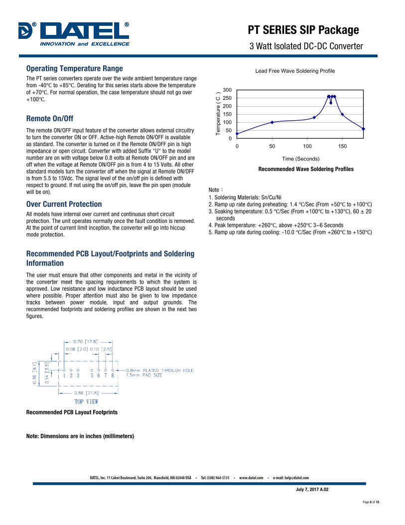
Recommended PCB Layout/Footprints and Soldering Information The user must ensure that other components and metal in the vicinity of the converter meet the spacing requirements to which the system is approved. Low resistance and low inductance PCB layout should be used where possible. Proper attention must also be given to low impedance tracks between power module, input and output grounds. The recommended footprints and soldering profiles are shown in the next two figures.
Recommended PCB Layout Footprints
Note: Dimensions are in inches (millimeters)
Recommended Wave Soldering Profiles Note: 1. Soldering Materials: Sn/Cu/Ni 2. Ramp up rate during preheating: 1.4 ℃/Sec (From +50℃ to +100℃) 3. Soaking temperature: 0.5 ℃/Sec (From +100℃ to +130℃), 60 ± 20
seconds 4. Peak temperature: +260℃, above +250℃ 3~6 Seconds 5. Ramp up rate during cooling: -10.0 ℃/Sec (From +260℃ to +150℃)
050
100150200250300
0 50 100 150
Tem
pera
ture
( C
)
Time (Seconds)
Lead Free Wave Soldering Profile
Page 6 of 15

July 7, 2017 A.02
PT SERIES SIP Package 3 Watt Isolated DC-DC Converter
Power De-Rating Curves for PT Series Note that operating ambient temperature range is -40℃ to + 85℃ with derating above 71℃. Also, the maximum case temperature under any operating condition should not exceed +100℃.
Page 7 of 15

July 7, 2017 A.02
PT SERIES SIP Package 3 Watt Isolated DC-DC Converter
Efficiency vs. Load Curves
PT5S3.3-0.7 PT5S5-0.6
PT5S12-0.25 PT5S15-0.2
PT5D5-0.3 PT5D12-0.12
PT5D15-0.1
Page 8 of 15

July 7, 2017 A.02
PT SERIES SIP Package 3 Watt Isolated DC-DC Converter
Efficiency vs. Load Curves
PT12S3.3-0.7 PT12S5-0.6
PT12S12-0.25 PT12S15-0.2
PT12D5-0.3 PT12D12-0.12
PT12D15-0.1
Page 9 of 15

July 7, 2017 A.02
PT SERIES SIP Package 3 Watt Isolated DC-DC Converter
PT24D15-0.1
PT24D12-0.12 PT24D5-0.3
PT24S15-0.2 PT24S12-0.25
PT24S5-0.6 PT24S3.3-0.7
Page 10 of 15

July 7, 2017 A.02
PT SERIES SIP Package 3 Watt Isolated DC-DC Converter
PT48D15-0.1
PT48D12-0.12
PT48S15-0.2 PT48S12-0.25
PT48S5-0.6 PT48S3.3-0.7
PT48D5-0.3
Page 11 of 15

July 7, 2017 A.02
PT SERIES SIP Package 3 Watt Isolated DC-DC Converter
Input Capacitance at the Power Module In order to avoid problems with loop stability, the converter must be connected to a low impedance AC source and a low inductance source. The input capacitors (Cin) should be placed close to the converter input pins to de-couple distribution inductance. The external input capacitors should have low ESR in order to quiet any ripple. Circuit as shown in the figure below represents typical measurement methods for reflected ripple current. The capacitor C1 and inductor L1 simulate the typical DC source impedance. The input reflected-ripple current is measured by a current probe oscilloscope with a simulated source Inductance (L1).
L1: 1uH C1: None Cin: 22uF ESR<0.7ohm @100KHz Input Reflected-Ripple Test Setup
Test Set-Up The basic test set-up to measure efficiency, load regulation, line regulation and other parameters is shown in the next figure. When testing the converter under any transient conditions, the user should ensure that the transient response of the source is sufficient to power the equipment under test. Below is the calculation of:
1- Efficiency 2- Load regulation 3- Line regulation
The value of efficiency is defined as:
%100×××
=ININ
OO
IVIVη
Where VO is output voltage, IO is output current, VIN is input voltage, IIN is input current.
The value of load regulation is defined as:
%100. ×−
=NL
NLFL
VVVregLoad
Where
VFL is the output voltage at full load VNL is the output voltage at 10% load
The value of line regulation is defined as:
%100. ×−
=LL
LLHL
VVVregLine
Where VHL is the output voltage of maximum input voltage at full load. VLL is the output voltage of minimum input voltage at full load.
PT Series Test Setup
Output Ripple and Noise Measurement The test set-up for noise and ripple measurements is shown in the figure below. A coaxial cable was used to prevent impedance mismatch reflections disturbing the noise readings at higher frequencies. Measurements are taken with the output appropriately loaded and all ripple/noise specifications are from D.C. to 20MHz Bandwidth.
+Vin
-Vin -Vo
+Vo
R-LoadC2Vin+
-
BNC
To ScopeC1
Note: C1: None C2: None
Output Voltage Ripple and Noise Measurement Set-Up
Output Capacitance The PT series converters provide unconditional stability with or without external capacitors. For good transient response, low ESR output capacitors should be located closer to the point of load.
Page 12 of 15

July 7, 2017 A.02
PT SERIES SIP Package 3 Watt Isolated DC-DC Converter
SAFETY and EMC Input Fusing and Safety Considerations The PT series of converters do not have an internal fuse. However, to achieve maximum safety and system protection, always use an input line fuse. We recommended a time delay fuse 2A for 24Vin, 1A for 12Vin, and 500mA for 24Vin and 48Vin models. The circuit in the figure below is recommended and it uses by a Transient Voltage Suppressor diode across the input terminal to protect the unit against surge or spike voltage and input reverse voltage.
Input Protection
EMC Considerations EMI Test standard: EN55022 Class A and Class B Conducted Emission Test Condition: Input Voltage: Nominal, Output Load: Full Load
Connection circuit for conducted EMI testing
EN55022 class A EN55022 class B EN55022 class A EN55022 class B Model No. C1 L1 Model No. C1 L1 Model No. C1 L1 Model No. C1 L1 PT5S3.3-0.7 10µF/16V 1206 2.2µH PT5S3.3-0.7 10µF/25V 1210 10µH PT24S3.3-0.7 4.7µF/50V 1812 12µH PT24S3.3-0.7 6.8µF/50V 1812 33µF
PT5S5-0.6 10µF/16V 1206 2.2µH PT5S5-0.6 10µF/25V 1210 10µH PT24S5-0.6 4.7µF/50V 1812 12µH PT24S5-0.6 6.8µF/50V 1812 33µF
PT512-0.25 10µF/16V 1206 2.2µH PT512-0.25 10µF/25V 1210 10µH PT2412-0.25 4.7µF/50V 1812 12µH PT2412-0.83 6.8µF/50V 1812 33µF
PT5S15-0.2 10µF/16V 1206 2.2µH PT5S15-0.2 10µF/25V 1210 10µH PT24S15-0.2 4.7µF/50V 1812 12µH PT24S15-0.2 6.8µF/50V 1812 33µF
PT5D5-0.3 10µF/16V 1206 2.2µH PT5D5-0.3 10µF/25V 1210 10µH PT24D5-0.3 4.7µF/50V 1812 12µH PT24D5-0.3 6.8µF/50V 1812 33µF
PT5D12-0.12 10µF/16V 1206 2.2µH PT5D12-0.12 10µF/25V 1210 10µH PT24D12-0.12 4.7µF/50V 1812 12µH PT24D12-0.12 6.8µF/50V 1812 33µF
PT5D15-0.1 10µF/16V 1206 2.2µH PT5D15-0.1 10µF/25V 1210 10µH PT24D15-0.1 4.7µF/50V 1812 12µH PT24D15-0.1 6.8µF/50V 1812 33µF
PT12S3.3-0.7 2.2µF/25V 1206 12µH PT12S3.3-0.7 2.2µF/25V 1210 33µH PT48S3.3-0.7 1µF/100V 1812 68µF PT48S3.3-0.7 2.2µF/100V 1812 150µF
PT12S5-0.6 2.2µF/25V 1206 12µH PT12S5-0.6 2.2µF/25V 1210 33µH PT48S5-0.6 1µF/100V 1812 68µF PT48S5-0.6 2.2µF/100V 1812 150µF
PT1212-0.25 2.2µF/25V 1206 12µH PT1212-0.25 2.2µF/25V 1210 33µH PT4812-0.25 1µF/100V 1812 68µF PT4812-0.83 2.2µF/100V 1812 150µF
PT12S15-0.2 2.2µF/25V 1206 12µH PT12S15-0.2 2.2µF/25V 1210 33µH PT48S15-0.2 1µF/100V 1812 68µF PT48S15-0.2 2.2µF/100V 1812 150µF
PT12D5-0.3 2.2µF/25V 1206 12µH PT12D5-0.3 2.2µF/25V 1210 33µH PT48D5-0.3 1µF/100V 1812 68µF PT48D5-0.3 2.2µF/100V 1812 150µF
PT12D12-0.12 2.2µF/25V 1206 12µH PT12D12-0.12 2.2µF/25V 1210 33µH PT48D12-0.12 1µF/100V 1812 68µF PT48D12-0.12 2.2µF/100V 1812 150µF
PT12D15-0.1 2.2µF/25V 1206 12µH PT12D15-0.1 2.2µF/25V 1210 33µH PT48D15-0.1 1µF/100V 1812 68µF PT48D15-0.1 2.2µF/100V 1812 150µF
Note: All of capacitors are ceramic capacitors
Page 13 of 15

July 7, 2017 A.02
PT SERIES SIP Package 3 Watt Isolated DC-DC Converter
EMI and conducted noise meet EN55022 Class A
Class A Test conducted for PT5S5-0.6 Class A Test conducted for PT12S12-2.5
Class A Test conducted for PT24D5-0.3 Class A Test conducted for PT48D12-0.12
EMI and conducted noise meet EN55022 Class B
Class B Test conducted for PT5S5-0.6 Class B Test conducted for PT12D5-0.3
Class B Test conducted for PT24S12-0.12 Class B Test conducted for PT48D15-0.1
Page 14 of 15

July 7, 2017 A.02
PT SERIES SIP Package 3 Watt Isolated DC-DC Converter
MECHANICAL SPECIFICATIONS
Note: All dimensions are in Inches (millimeters). Tolerance: x.xx ±0.02 in. (0.5mm), x.xxx ±0.010 in. (0.25 mm) unless otherwise noted
PIN CONNECTIONS
PIN CONNECTIONS PIN SINGLE OUTPUT DUAL OUTPUTS
1 - V Input - V Input
2 +V Input +V Input 3 On / Off On / Off 5 No Connection No Connection 6 +V Output +V Output 7 -V Output Common 8 No Connection -V output
PART NUMBER ORDERING INFORMATION
PT
Nominal Input voltage
24
Number of Outputs
S 5 0.6 U
(4.5-9) 5 Volts
(9-18) 12 Volts
(18-36) 24 Volts
(36-75) 48 Volts
S- Single
D- Dual
Note: For proper part ordering, enter option suffixes in order listed in table above
Family, Form Factor Package Voltage Output Volts Current Output (A) Options
None – No Under Voltage Protection
U- Under Voltage Protection
(See Remote On/Off description)
3.3 Volts – 3.3
5 Volts – 5
12 Volts – 12
15 Volts – 15
±5 Volts - 5
±12 Volts - 12
±15 Volts - 15
3.3 Volts – 0.7
5 Volts – 0.6
12 Volts – 0.25
15 Volts – 0.2
±5 Volts - 0.3
±12 Volts - 0.12
±15 Volts - 0.1
Page 15 of 15