
PSP 102 - Pennsylvania State University
112
Issued: 10/2006 PSP 102.1 The PSP model is a joint development of Arizona State University and NXP Semiconductors Research G.D.J. Smit, A.J. Scholten, and D.B.M. Klaassen (NXP Semiconductors) R. van Langevelde (Philips Research Europe) G. Gildenblat, X. Li, and W. Wu (Arizona State University) Unclassified Report c NXP Semiconductors 2006
Transcript of PSP 102 - Pennsylvania State University
Issued: 10/2006
PSP 102.1
The PSP model is a joint development of Arizona State University andNXP Semiconductors Research
G.D.J. Smit, A.J. Scholten, and D.B.M. Klaassen
(NXP Semiconductors)
R. van Langevelde (Philips Research Europe)
G. Gildenblat, X. Li, and W. Wu
(Arizona State University)
Unclassified Report
c© NXP Semiconductors 2006
October 2006 PSP 102.1 Unclassified Report
Concerns:
Period of Work: 2005-2006
Notebooks: None
PSP developers
• At NXP semiconductors Research (formerly Philips Research Europe)
– Geert D.J. Smit
– Andries J. Scholten
– Dirk B.M. Klaassen
• At Philips Research Europe
– Ronald van Langevelde
• At Arizona State University (formerly at The Pennsylvania State University)
– Gennady Gildenblat
– Hailing Wang (until 2005)
– Xin Li
– Weimin Wu
Authors’ address G.D.J. Smit [email protected]. Scholten [email protected]. Klaassen [email protected]. Gildenblat [email protected]
c© NXP SEMICONDUCTORS 2006All rights reserved. Reproduction or dissemination in whole or in part is prohibited without theprior written consent of the copyright holder.
ii c© NXP Semiconductors 2006
Unclassified Report PSP 102.1 October 2006
Title: PSP 102.1
Author(s): G.D.J. Smit, A.J. Scholten, and D.B.M. Klaassen (NXP Research)Ronald van Langevelde (Philips Research Europe)G. Gildenblat, X. Li, and W. Wu (Arizona State University)
Reviewer(s):
Technical Note: TN-
AdditionalNumbers:
Subcategory:
Project: Compact modeling
Customer: NXP Semiconductors
Keywords: PSP Model, compact modeling, MOSFET, CMOS, circuit simulation, integrated circuits
Abstract: The PSP model is a compact MOSFET model intended for digital, analogue, and RF-design, which is jointly developed by NXP Semiconductors (formerly part of Philips)and Arizona State University (formerly at The Pennsylvania State University). The rootsof PSP lie in both MOS Model 11 (developed by Philips Research) and SP (developedby Penn State University). PSP is a surface-potential based MOS Model, containingall relevant physical effects (mobility reduction, velocity saturation, DIBL, gate current,lateral doping gradient effects, STI stress, etc.) to model present-day and upcoming deep-submicron bulk CMOS technologies. A source/drain junction model, c.q. the JUNCAP2model, is an integrated part of PSP. This report contains a full description of the PSPmodel, including parameter sets, scaling rules, model equations, and a description of theparameter extraction procedure.In December 2005, the Compact Model Council (CMC) has elected PSP as the newindustrial standard model for compact MOSFET modeling.
c© NXP Semiconductors 2006 iii
October 2006 PSP 102.1 Unclassified Report
iv c© NXP Semiconductors 2006
Unclassified Report PSP 102.1 October 2006
History of model and documentation
History of the model
April 2005 Release of PSP 100.0 (which includes JUNCAP2 200.0) as part of SiMKit 2.1. A Verilog-Aimplementation of the PSP-model is made available as well. The PSP-NQS model is released as Verilog-Acode only.
August 2005 Release of PSP 100.1 (which includes JUNCAP2 200.1) as part of SiMKit 2.2. Similar tothe previous version, a Verilog-A implementation of the PSP-model is made available as well and the PSP-NQS model is released as Verilog-A code only. Focus of this release was mainly on the optimization of theevaluation speed of PSP. Moreover, the PSP implementation has been extended with operating point output(SiMKit-version only).
March 2006 Release of PSP 101.0 (which includes JUNCAP2 200.1) as part of SiMKit 2.3. PSP 101.0 isnot backward compatible with PSP 100.1. Similar to the previous version, a Verilog-A implementation of thePSP-model is made available as well and the PSP-NQS model is released as Verilog-A code only. Focus of thisrelease was on the implementation of requirements for CMC standardization, especially those which could notpreserve backward compatibility.
June 2006 Release of PSP 102.0 (which includes JUNCAP2 200.1) as part of SiMKit 2.3.2. PSP 102.0 isbackward compatible with PSP 101.0 in all practical cases, provided a simple transformation to the parameterset is applied (see description below). Similar to the previous version, a Verilog-A implementation of thePSP-model is made available as well and the PSP-NQS model is released as Verilog-A code only.
Global parameter sets for PSP 101.0 can be transformed to PSP 102.0 by replacing DPHIBL (in 102.0 para-meter set) by DPHIBO ·DPHIBL (from 101.0 parameter set). After this transformation, the simulation resultsof PSP 102.0 are identical to those of PSP 101.0 in all practical situations.
October 2006 Release of PSP 102.1 (which includes JUNCAP2 200.2) as part of SiMKit 2.4. PSP 102.1is backward compatible with PSP 102.0. SiMKit 2.4 includes a preliminary implementation of the PSP-NQSmodel. Similar to the previous version, a Verilog-A implementation of the PSP-model is available as well. Themain changes are:
• Added clipping boundaries for SWNQS
• Several minor changes and improvements in model implementation
• Solved bug in stress model
• Solved bug in JUNCAP2
• Included preliminary implementation of PSP-NQS in SiMKit. This implementation thereby circumventsthe problem of the Verilog-A code being too large to compile in Spectre. Moreover, it is computationallymore efficient as it uses less rows in the simulator matrix. On the other hand, this implementation hassome known limitations. For more details, please contact one of the authors. Further improvements areexpected in future releases.
History of the documentation
April 2005 First release of PSP (PSP 100.0) documentation.
August 2005 Documentation updated for PSP 100.1, errors corrected and new items added.
c© NXP Semiconductors 2006 v
October 2006 PSP 102.1 Unclassified Report
March 2006 Documentation adapted to PSP 101.0. Added more details on noise-model implementation anda full description of the NQS-model.
June 2006 Documentation adapted to PSP 102.0 and some errors corrected.
October 2006 Documentation adapted to PSP 102.1 and some errors corrected.
vi c© NXP Semiconductors 2006
Unclassified Report PSP 102.1 October 2006
Contents
1 Introduction 1
1.1 Origin and purpose . . . . . . . . . . . . . . . . . . . . . . . . . . . . . . . . . . . . . . . . 1
1.2 Structure of PSP . . . . . . . . . . . . . . . . . . . . . . . . . . . . . . . . . . . . . . . . . . 1
1.3 Availability . . . . . . . . . . . . . . . . . . . . . . . . . . . . . . . . . . . . . . . . . . . . 2
1.3.1 SiMKit . . . . . . . . . . . . . . . . . . . . . . . . . . . . . . . . . . . . . . . . . . 3
2 Constants and Parameters 4
2.1 Nomenclature . . . . . . . . . . . . . . . . . . . . . . . . . . . . . . . . . . . . . . . . . . . 4
2.2 Parameter clipping . . . . . . . . . . . . . . . . . . . . . . . . . . . . . . . . . . . . . . . . 4
2.3 Circuit simulator variables . . . . . . . . . . . . . . . . . . . . . . . . . . . . . . . . . . . . 4
2.4 Model constants . . . . . . . . . . . . . . . . . . . . . . . . . . . . . . . . . . . . . . . . . . 5
2.5 Model parameters . . . . . . . . . . . . . . . . . . . . . . . . . . . . . . . . . . . . . . . . . 5
2.5.1 Instance parameters at global level . . . . . . . . . . . . . . . . . . . . . . . . . . . . 6
2.5.2 Instance parameters at local level . . . . . . . . . . . . . . . . . . . . . . . . . . . . 7
2.5.3 Parameters for physical geometrical scaling rules (global model) . . . . . . . . . . . . 9
2.5.4 Parameters for binning model . . . . . . . . . . . . . . . . . . . . . . . . . . . . . . 15
2.5.5 Parameters for stress model . . . . . . . . . . . . . . . . . . . . . . . . . . . . . . . 25
2.5.6 Parameters for local model . . . . . . . . . . . . . . . . . . . . . . . . . . . . . . . . 27
2.5.7 Parameters for source-bulk and drain-bulk junction model . . . . . . . . . . . . . . . 30
3 Geometry and Stress dependence 33
3.1 Introduction . . . . . . . . . . . . . . . . . . . . . . . . . . . . . . . . . . . . . . . . . . . . 33
3.2 Geometrical scaling rules . . . . . . . . . . . . . . . . . . . . . . . . . . . . . . . . . . . . . 33
3.3 Binning equations . . . . . . . . . . . . . . . . . . . . . . . . . . . . . . . . . . . . . . . . . 40
3.4 Parameter modification due to stress effects . . . . . . . . . . . . . . . . . . . . . . . . . . . 47
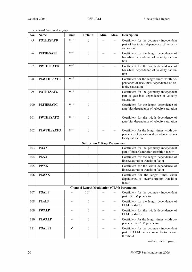
3.4.1 Layout effects for regular shapes . . . . . . . . . . . . . . . . . . . . . . . . . . . . . 47
3.4.2 Layout effects for irregular shapes . . . . . . . . . . . . . . . . . . . . . . . . . . . . 47
3.4.3 Calculation of parameter modifications . . . . . . . . . . . . . . . . . . . . . . . . . 47
4 PSP Model Equations 51
4.1 Internal Parameters (including Temperature Scaling) . . . . . . . . . . . . . . . . . . . . . . 51
4.2 Model Equations . . . . . . . . . . . . . . . . . . . . . . . . . . . . . . . . . . . . . . . . . 55
4.2.1 Conditioning of Terminal Voltages . . . . . . . . . . . . . . . . . . . . . . . . . . . . 55
c© NXP Semiconductors 2006 vii
October 2006 PSP 102.1 Unclassified Report
4.2.2 Bias-Dependent Body Factor . . . . . . . . . . . . . . . . . . . . . . . . . . . . . . . 55
4.2.3 Surface Potential at Source Side and Related Variables . . . . . . . . . . . . . . . . . 55
4.2.4 Drain Saturation Voltage . . . . . . . . . . . . . . . . . . . . . . . . . . . . . . . . . 57
4.2.5 Surface Potential at Drain Side and Related Variables . . . . . . . . . . . . . . . . . . 58
4.2.6 Mid-Point Surface Potential and Related Variables . . . . . . . . . . . . . . . . . . . 59
4.2.7 Polysilicon Depletion . . . . . . . . . . . . . . . . . . . . . . . . . . . . . . . . . . . 60
4.2.8 Potential Mid-Point Inversion Charge and Related Variables . . . . . . . . . . . . . . 61
4.2.9 Drain-Source Channel Current . . . . . . . . . . . . . . . . . . . . . . . . . . . . . . 61
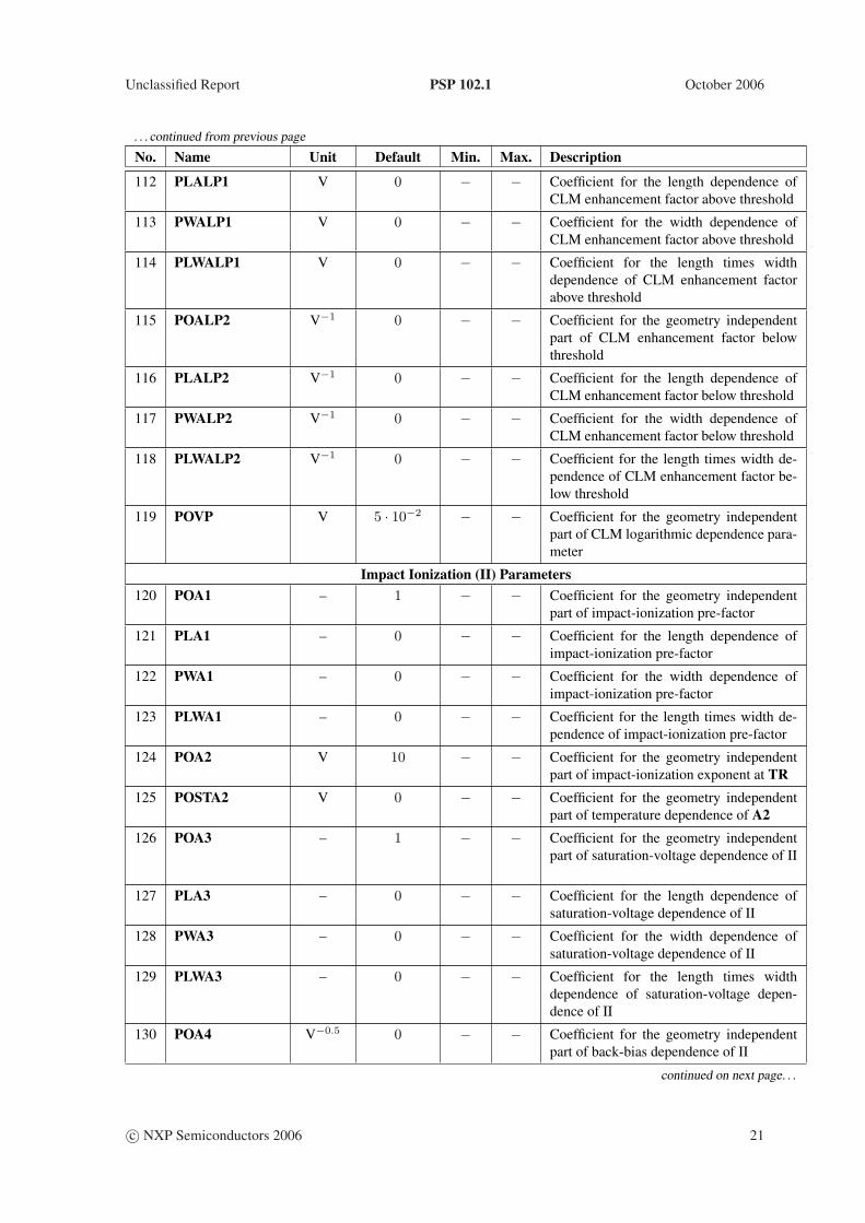
4.2.10 Auxiliary Variables for Calculation of Intrinsic Charges and Gate Current . . . . . . . 62
4.2.11 Impact Ionization or Weak-Avalanche . . . . . . . . . . . . . . . . . . . . . . . . . . 62
4.2.12 Surface Potential in Gate Overlap Regions . . . . . . . . . . . . . . . . . . . . . . . . 63
4.2.13 Gate Current . . . . . . . . . . . . . . . . . . . . . . . . . . . . . . . . . . . . . . . 64
4.2.14 Gate-Induced Drain/Source Leakage Current . . . . . . . . . . . . . . . . . . . . . . 65
4.2.15 Total Terminal Currents . . . . . . . . . . . . . . . . . . . . . . . . . . . . . . . . . 66
4.2.16 Quantum-Mechanical Corrections . . . . . . . . . . . . . . . . . . . . . . . . . . . . 67
4.2.17 Intrinsic Charge Model . . . . . . . . . . . . . . . . . . . . . . . . . . . . . . . . . . 67
4.2.18 Extrinsic Charge Model . . . . . . . . . . . . . . . . . . . . . . . . . . . . . . . . . 67
4.2.19 Total Terminal Charges . . . . . . . . . . . . . . . . . . . . . . . . . . . . . . . . . . 68
4.2.20 Noise Model . . . . . . . . . . . . . . . . . . . . . . . . . . . . . . . . . . . . . . . 69
5 Non-quasi-static RF model 71
5.1 Introduction . . . . . . . . . . . . . . . . . . . . . . . . . . . . . . . . . . . . . . . . . . . . 71
5.2 NQS-effects . . . . . . . . . . . . . . . . . . . . . . . . . . . . . . . . . . . . . . . . . . . . 71
5.3 Parasitics circuit . . . . . . . . . . . . . . . . . . . . . . . . . . . . . . . . . . . . . . . . . . 71
5.4 NQS and RF parameters . . . . . . . . . . . . . . . . . . . . . . . . . . . . . . . . . . . . . 72
5.4.1 Additional Parameters for global NQS model . . . . . . . . . . . . . . . . . . . . . . 73
5.4.2 Additional Parameters for local NQS model . . . . . . . . . . . . . . . . . . . . . . . 73
5.4.3 Geometrical Scaling Rules . . . . . . . . . . . . . . . . . . . . . . . . . . . . . . . . 73
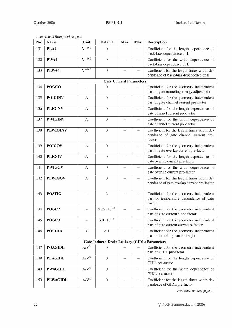
5.5 NQS Model Equations . . . . . . . . . . . . . . . . . . . . . . . . . . . . . . . . . . . . . . 74
5.5.1 Internal constants . . . . . . . . . . . . . . . . . . . . . . . . . . . . . . . . . . . . . 74
5.5.2 Position independent quantities . . . . . . . . . . . . . . . . . . . . . . . . . . . . . 75
5.5.3 Position dependent surface potential and charge . . . . . . . . . . . . . . . . . . . . . 75
5.5.4 Cubic spline interpolation . . . . . . . . . . . . . . . . . . . . . . . . . . . . . . . . 77
5.5.5 Continuity equation . . . . . . . . . . . . . . . . . . . . . . . . . . . . . . . . . . . . 77
5.5.6 Non-quasi-static terminal charges . . . . . . . . . . . . . . . . . . . . . . . . . . . . 78
6 Embedding 80
6.1 Model selection . . . . . . . . . . . . . . . . . . . . . . . . . . . . . . . . . . . . . . . . . . 80
6.2 Case of parameters . . . . . . . . . . . . . . . . . . . . . . . . . . . . . . . . . . . . . . . . 80
6.3 Embedding PSP in a Circuit Simulator . . . . . . . . . . . . . . . . . . . . . . . . . . . . . . 80
6.4 Integration of JUNCAP2 in PSP . . . . . . . . . . . . . . . . . . . . . . . . . . . . . . . . . 81
6.5 Verilog-A versus C . . . . . . . . . . . . . . . . . . . . . . . . . . . . . . . . . . . . . . . . 84
viii c© NXP Semiconductors 2006
Unclassified Report PSP 102.1 October 2006
6.5.1 Implementation of GMIN . . . . . . . . . . . . . . . . . . . . . . . . . . . . . . . . 84
6.5.2 Implementation of the noise-equations . . . . . . . . . . . . . . . . . . . . . . . . . . 84
7 Parameter extraction 87
7.1 Measurements . . . . . . . . . . . . . . . . . . . . . . . . . . . . . . . . . . . . . . . . . . . 87
7.2 Extraction of local parameters at room temperature . . . . . . . . . . . . . . . . . . . . . . . 88
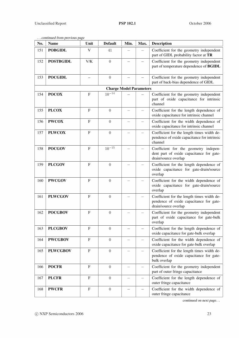
7.3 Extraction of Temperature Scaling Parameters . . . . . . . . . . . . . . . . . . . . . . . . . . 91
7.4 Extraction of Geometry Scaling Parameters . . . . . . . . . . . . . . . . . . . . . . . . . . . 93
7.5 Summary – Geometrical scaling . . . . . . . . . . . . . . . . . . . . . . . . . . . . . . . . . 95
7.6 Extraction of Binning Parameters . . . . . . . . . . . . . . . . . . . . . . . . . . . . . . . . . 95
8 DC Operating Point Output 97
A Auxiliary Equations 102
c© NXP Semiconductors 2006 ix

Unclassified Report PSP 102.1 October 2006
Section 1
Introduction
1.1 Origin and purpose
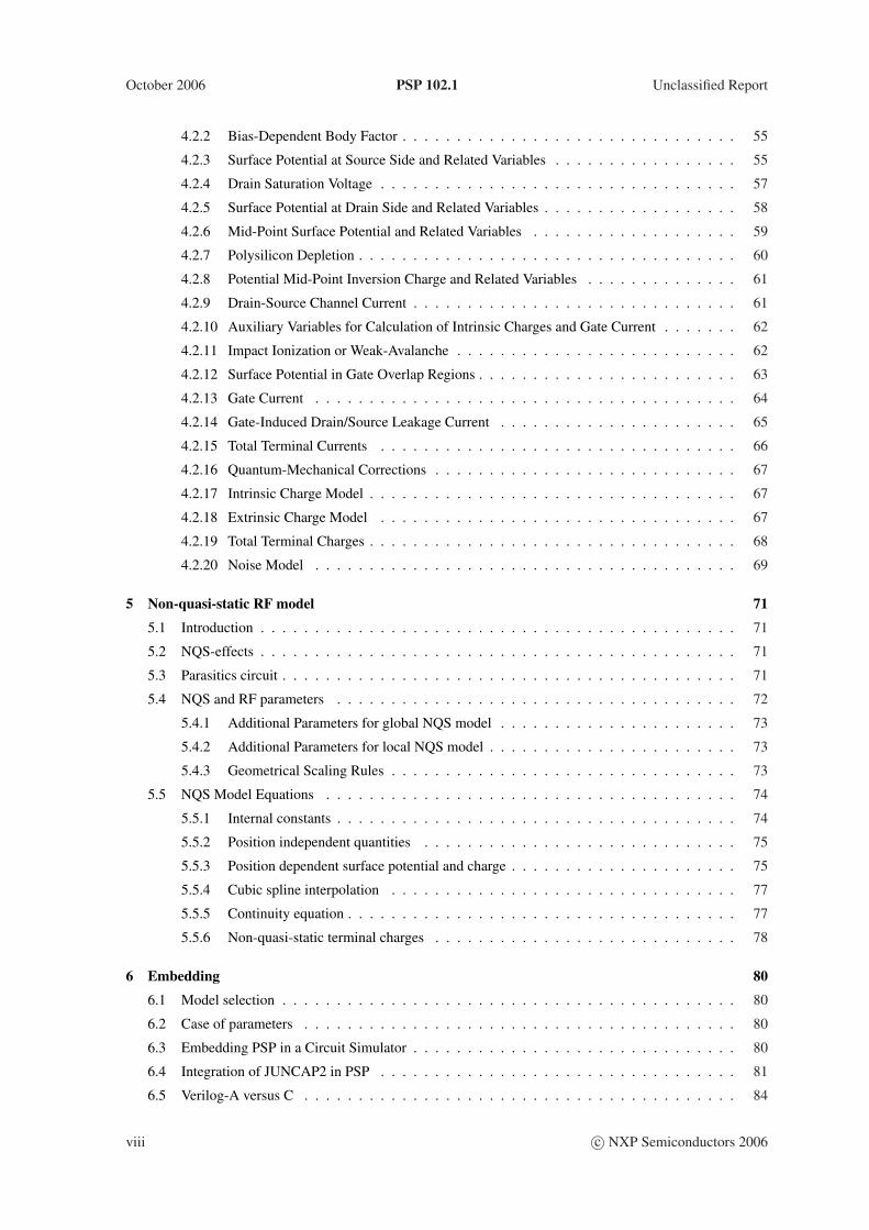
The PSP model is a compact MOSFET model intended for digital, analogue, and RF-design, which is jointlydeveloped by NXP Semiconductors Research (formerly part of Philips) and Arizona State University (formerlyat The Pennsylvania State University). The roots of PSP lie in both MOS Model 11 (developed by Philips)and SP (developed by Penn State University). PSP is a surface-potential based MOS Model, containing allrelevant physical effects (mobility reduction, velocity saturation, DIBL, gate current, lateral doping gradienteffects, STI stress, etc.) to model present-day and upcoming deep-submicron bulk CMOS technologies. Thesource/drain junction model, c.q. the JUNCAP2 model, is fully integrated in PSP.
PSP not only gives an accurate description of currents, charges, and their first order derivatives (i.e. transcon-ductance, conductance and capacitances), but also of the higher order derivatives, resulting in an accuratedescription of electrical distortion behavior. The latter is especially important for analog and RF circuit design.The model furthermore gives an accurate description of the noise behavior of MOSFETs. Finally, PSP has anoption for simulation of non-quasi-static (NQS) effects.
The source code of PSP and the most recent version of this documentation are available on the PSP model website pspmodel.asu.edu and the NXP Semiconductors web site: www.nxp.com/philips_models.
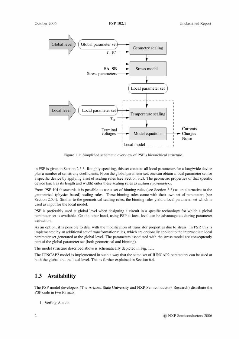
1.2 Structure of PSP
The PSP model has a hierarchical structure, similar to that of MOS Model 11 and SP. This means that there isa strict separation of the geometry scaling in the global model and the model equations in the local model.
As a consequence, PSP can be used at either one of two levels.
• Global level One uses a global parameter set, which describes a whole geometry range. Combinedwith instance parameters (such as L and W ), a local parameter set is internally generated and furtherprocessed at the local level in exactly the same way as a custom-made local parameter set.
• Local level One uses a custom-made local parameter set to simulate a transistor with a specific geometry.Temperature scaling is included at this level.
The set of parameters which occur in the equations for the various electrical quantities is called the localparameter set. In PSP, temperature scaling parameters are included in the local parameter set. An overview ofthe local parameters in PSP is given in Section 2.5.6. Each of these parameters can be determined by purelyelectrical measurements. As a consequence, a local parameter set gives a complete description of the electricalproperties of a device of one particular geometry.
Since most of these (local) parameters scale with geometry, all transistors of a particular process can be de-scribed by a (larger) set of parameters, called the global parameter set. An overview of the global parameters
c© NXP Semiconductors 2006 1
October 2006 PSP 102.1 Unclassified Report
Local parameter set
Temperature scalingLocal parameter set
Model equationsCurrentsChargesNoise
Terminalvoltages
TA
Local model
Stress modelStress parameters
SA, SB
Geometry scalingL, W
Global parameter setGlobal level
Local level
Figure 1.1: Simplified schematic overview of PSP’s hierarchical structure.
in PSP is given in Section 2.5.3. Roughly speaking, this set contains all local parameters for a long/wide deviceplus a number of sensitivity coefficients. From the global parameter set, one can obtain a local parameter set fora specific device by applying a set of scaling rules (see Section 3.2). The geometric properties of that specificdevice (such as its length and width) enter these scaling rules as instance parameters.
From PSP 101.0 onwards it is possible to use a set of binning rules (see Section 3.3) as an alternative to thegeometrical (physics based) scaling rules. These binning rules come with their own set of parameters (seeSection 2.5.4). Similar to the geometrical scaling rules, the binning rules yield a local parameter set which isused as input for the local model.
PSP is preferably used at global level when designing a circuit in a specific technology for which a globalparameter set is available. On the other hand, using PSP at local level can be advantageous during parameterextraction.
As an option, it is possible to deal with the modification of transistor properties due to stress. In PSP, this isimplemented by an additional set of transformation rules, which are optionally applied to the intermediate localparameter set generated at the global level. The parameters associated with the stress model are consequentlypart of the global parameter set (both geometrical and binning).
The model structure described above is schematically depicted in Fig. 1.1.
The JUNCAP2 model is implemented in such a way that the same set of JUNCAP2 parameters can be used atboth the global and the local level. This is further explained in Section 6.4.
1.3 Availability
The PSP model developers (The Arizona State University and NXP Semiconductors Research) distribute thePSP code in two formats:
1. Verilog-A code
2 c© NXP Semiconductors 2006
Unclassified Report PSP 102.1 October 2006
2. C-code (as part of SiMKit)
The C-version is automatically generated from the Verilog-A version by a software package called ADMS [1].This procedure guarantees the two implementations to contain identical equations. Nevertheless—due to somespecific limitations/capabilities of the two formats—there are a few minor differences, which are described inSection 6.5.
1.3.1 SiMKit
SiMKit is a simulator-independent compact transistor model library. Simulator-specific connections are handledthrough so-called adapters that provide the correct interfacing to the circuit simulator of choice. Currently,adapters to the following circuit simulators are provided:
1. Spectre (Cadence)
2. Pstar (Philips/NXP)
3. ADS (Agilent)
c© NXP Semiconductors 2006 3
October 2006 PSP 102.1 Unclassified Report
Section 2
Constants and Parameters
2.1 Nomenclature
The nomenclature of the quantities listed in the following sections has been chosen to express their purposeand their relation to other quantities and to preclude ambiguity and inconsistency. Throughout this document,all PSP parameter names are printed in boldface capitals. Parameters which refer to the long transistor limitand/or the reference temperature have a name containing an ‘O’, while the names of scaling parameters endwith the letter ‘L’ and/or ‘W’ for length or width scaling, respectively. Parameters for temperature scaling startwith ‘ST’, followed by the name of the parameter to which the temperature scaling applies. Parameters usedfor the binning model start with ‘PO’, ‘PL’, ‘PW’, or ‘PLW’, followed by the name of the local parameterthey refer to.
2.2 Parameter clipping
For most parameters, a maximum and/or minimum value is given in the tables below. In PSP, all parametersare limited (clipped) to this pre-specified range in order to prevent difficulties in the numerical evaluation ofthe model, such as division by zero.
N.B. After computation of the scaling rules (either physical or binning) and stress equations, the resulting localparameters are subjected to the clipping values as given in Section 2.5.6.
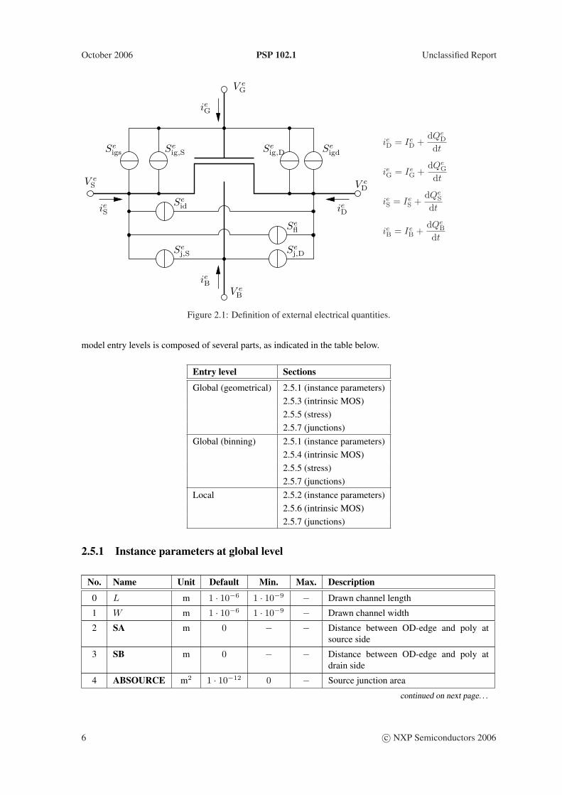
2.3 Circuit simulator variables
External electrical variables
The definitions of the external electrical variables are illustrated in Fig. 2.1. The relationship between theseexternal variables and the internal variables used in Chapter 4 is given in Fig. 6.1.
Symbol Unit Description
V eD V Potential applied to drain node
V eG V Potential applied to gate node
V eS V Potential applied to source node
V eB V Potential applied to bulk node
IeD A DC current into drain node
IeG A DC current into gate node
continued on next page. . .
4 c© NXP Semiconductors 2006
Unclassified Report PSP 102.1 October 2006
. . . continued from previous page
Symbol Unit Description
IeS A DC current into source node
IeB A DC current into bulk node
Sefl A2s Spectral density of flicker noise current in the channel
Seid A2s Spectral density of thermal noise current in the channel
Seig,S A2s Spectral density of induced gate noise at source side
Seig,D A2s Spectral density of induced gate noise at drain side
Seigs A2s Spectral density of gate current shot noise at source side
Seigd A2s Spectral density of gate current shot noise at drain side
Sej,S A2s Spectral density of source junction shot noise
Sej,D A2s Spectral density of drain junction shot noise
Seigid A2s Cross spectral density between Se
id and (SeigS or Se
igD)
Other circuit simulator variables
Next to the electrical variables described above, the quantities in the table below are also provided to the modelby the circuit simulator.
Symbol Unit Description
TAC Ambient circuit temperature
fop Hz Operation frequency
2.4 Model constants
In the following table the symbolic representation, the value and the description of the various physical con-stants used in the PSP model are given.
No. Symbol Unit Value Description
1 T0 K 273.15 Offset between Celsius and Kelvin tempera-ture scale
2 kB J/K 1.3806505 · 10−23 Boltzmann constant3 ~ J s 1.05457168 · 10−34 Reduced Planck constant4 q C 1.6021918 · 10−19 Elementary unit charge5 m0 kg 9.1093826 · 10−31 Electron rest mass6 εox F/m 3.453 · 10−11 Absolute permittivity of oxide7 εSi F/m 1.045 · 10−10 Absolute permittivity of silicon8 QMN V m
43 C−
23 5.951993 Constant of quantum-mechanical behavior of
electrons9 QMP V m
43 C−
23 7.448711 Constant of quantum-mechanical behavior of
holes
2.5 Model parameters
In this section all parameters of the PSP-model are described. The parameters for the intrinsic MOS model, thestress model and the junction model are given in separate tables. The complete parameter list for each of the
c© NXP Semiconductors 2006 5
October 2006 PSP 102.1 Unclassified Report
SeigdSe
igs Seig,S Se
ig,D
Seid
Sej,S Se
j,D
Sefl
V eG
V eD
V eB
V eS
ieG
ieD
ieB
ieS
ieD = IeD +
dQeD
dt
ieG = IeG +
dQeG
dt
ieS = IeS +
dQeS
dt
ieB = IeB +
dQeB
dt
Figure 2.1: Definition of external electrical quantities.
model entry levels is composed of several parts, as indicated in the table below.
Entry level Sections
Global (geometrical) 2.5.1 (instance parameters)2.5.3 (intrinsic MOS)2.5.5 (stress)2.5.7 (junctions)
Global (binning) 2.5.1 (instance parameters)2.5.4 (intrinsic MOS)2.5.5 (stress)2.5.7 (junctions)
Local 2.5.2 (instance parameters)2.5.6 (intrinsic MOS)2.5.7 (junctions)
2.5.1 Instance parameters at global level
No. Name Unit Default Min. Max. Description
0 L m 1 · 10−6 1 · 10−9 − Drawn channel length
1 W m 1 · 10−6 1 · 10−9 − Drawn channel width
2 SA m 0 − − Distance between OD-edge and poly atsource side
3 SB m 0 − − Distance between OD-edge and poly atdrain side
4 ABSOURCE m2 1 · 10−12 0 − Source junction area
continued on next page. . .
6 c© NXP Semiconductors 2006
Unclassified Report PSP 102.1 October 2006
. . . continued from previous page
No. Name Unit Default Min. Max. Description
5 LSSOURCE m 1 · 10−6 0 − STI-edge part of source junction perimeter
6 LGSOURCE m 1 · 10−6 0 − Gate-edge part of source junction perime-ter
7 ABDRAIN m2 1 · 10−12 0 − Drain junction area
8 LSDRAIN m 1 · 10−6 0 − STI-edge part of drain junction perimeter
9 LGDRAIN m 1 · 10−6 0 − Gate-edge part of drain junction perimeter
10 AS m2 1 · 10−12 0 − Source junction area (alternative spec.)
11 PS m 1 · 10−6 0 − Source STI-edge perimeter (alternativespec.)
12 AD m2 1 · 10−12 0 − Drain junction area (alternative spec.)
13 PD m 1 · 10−6 0 − Drain STI-edge perimeter (alternativespec.)
14 MULT – 1 0 − Number of devices in parallel
Note that if both SA and SB are set to 0, the stress-equations are not computed.
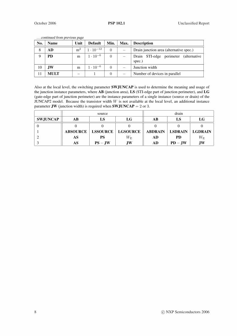
The switching parameter SWJUNCAP is used to determine the meaning and usage of the junction instanceparameters, where AB (junction area), LS (STI-edge part of junction perimeter), and LG (gate-edge part ofjunction perimeter) are the instance parameters of a single instance (source or drain) of the JUNCAP2 model.
source drainSWJUNCAP AB LS LG AB LS LG
0 0 0 0 0 0 01 ABSOURCE LSSOURCE LGSOURCE ABDRAIN LSDRAIN LGDRAIN2 AS PS WE AD PD WE
3 AS PS−WE WE AD PD−WE WE
2.5.2 Instance parameters at local level
As explained in Section 6.4, the instance parameters for the JUNCAP2 model are used at the local level as well.
No. Name Unit Default Min. Max. Description
0 ABSOURCE m2 1 · 10−12 0 − Source junction area
1 LSSOURCE m 1 · 10−6 0 − STI-edge part of source junction perimeter
2 LGSOURCE m 1 · 10−6 0 − Gate-edge part of source junction perime-ter
3 ABDRAIN m2 1 · 10−12 0 − Drain junction area
4 LSDRAIN m 1 · 10−6 0 − STI-edge part of drain junction perimeter
5 LGDRAIN m 1 · 10−6 0 − Gate-edge part of drain junction perimeter
6 AS m2 1 · 10−12 0 − Source junction area (alternative spec.)
7 PS m 1 · 10−6 0 − Source STI-edge perimeter (alternativespec.)
continued on next page. . .
c© NXP Semiconductors 2006 7
October 2006 PSP 102.1 Unclassified Report
. . . continued from previous page
No. Name Unit Default Min. Max. Description
8 AD m2 1 · 10−12 0 − Drain junction area (alternative spec.)
9 PD m 1 · 10−6 0 − Drain STI-edge perimeter (alternativespec.)
10 JW m 1 · 10−6 0 − Junction width
11 MULT – 1 0 − Number of devices in parallel
Also at the local level, the switching parameter SWJUNCAP is used to determine the meaning and usage ofthe junction instance parameters, where AB (junction area), LS (STI-edge part of junction perimeter), and LG(gate-edge part of junction perimeter) are the instance parameters of a single instance (source or drain) of theJUNCAP2 model. Because the transistor width W is not available at the local level, an additional instanceparameter JW (junction width) is required when SWJUNCAP = 2 or 3.
source drainSWJUNCAP AB LS LG AB LS LG
0 0 0 0 0 0 01 ABSOURCE LSSOURCE LGSOURCE ABDRAIN LSDRAIN LGDRAIN2 AS PS WE AD PD WE
3 AS PS− JW JW AD PD− JW JW
8 c© NXP Semiconductors 2006
Unclassified Report PSP 102.1 October 2006
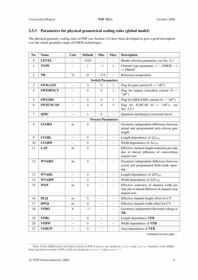
2.5.3 Parameters for physical geometrical scaling rules (global model)
The physical geometry scaling rules of PSP (see Section 3.2) have been developed to give a good descriptionover the whole geometry range of CMOS technologies.
No. Name Unit Default Min. Max. Description
0 LEVEL – 1020 − − Model selection parameter; see Sec. 6.1
1 TYPE – 1 −1 1 Channel type parameter; 1 ↔ NMOS, −1↔ PMOS1
2 TR C 21 −273 − Reference temperature
Switch Parameters3 SWIGATE – 0 0 1 Flag for gate current (0 ↔ “off”)
4 SWIMPACT – 0 0 1 Flag for impact ionization current (0 ↔“off”)
5 SWGIDL – 0 0 1 Flag for GIDL/GISL current (0 ↔ “off”)
6 SWJUNCAP – 0 0 3 Flag for JUNCAP (0 ↔ “off”); seeSec. 2.5.1
7 QMC – 1 0 − Quantum-mechanical correction factor
Process Parameters8 LVARO m 0 − − Geometry independent difference between
actual and programmed poly-silicon gatelength
9 LVARL – 0 − − Length dependence of ∆LPS
10 LVARW – 0 − − Width dependence of ∆LPS
11 LAP m 0 − − Effective channel length reduction per sidedue to lateral diffusion of source/draindopant ions
12 WVARO m 0 − − Geometry independent difference betweenactual and programmed field-oxide open-ing
13 WVARL – 0 − − Length dependence of ∆WOD
14 WVARW – 0 − − Width dependence of ∆WOD
15 WOT m 0 − − Effective reduction of channel width perside due to lateral diffusion of channel-stopdopant ions
16 DLQ m 0 − − Effective channel length offset for CV
17 DWQ m 0 − − Effective channel width offset for CV
18 VFBO V −1 − − Geometry-independent flat-band voltage atTR
19 VFBL – 0 − − Length dependence VFB20 VFBW – 0 − − Width dependence of VFB21 VFBLW – 0 − − Area dependence of VFB
continued on next page. . .
1Note: In the SiMKit-based and built-in version of PSP in Spectre one should use type=n and type=p. Similarly, in the SiMKit-based and built-in version of PSP in ADS one should use gender=1 and gender=-1.
c© NXP Semiconductors 2006 9
October 2006 PSP 102.1 Unclassified Report
. . . continued from previous page
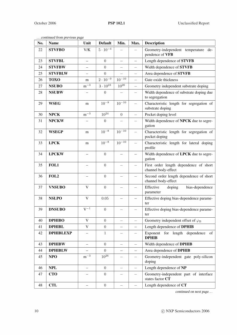
No. Name Unit Default Min. Max. Description
22 STVFBO V/K 5 · 10−4 − − Geometry-independent temperature de-pendence of VFB
23 STVFBL – 0 − − Length dependence of STVFB24 STVFBW – 0 − − Width dependence of STVFB25 STVFBLW – 0 − − Area dependence of STVFB26 TOXO m 2 · 10−9 10−10 − Gate oxide thickness
27 NSUBO m−3 3 · 1023 1020 − Geometry independent substrate doping
28 NSUBW – 0 − − Width dependence of substrate doping dueto segregation
29 WSEG m 10−8 10−10 − Characteristic length for segregation ofsubstrate doping
30 NPCK m−3 1024 0 − Pocket doping level
31 NPCKW – 0 − − Width dependence of NPCK due to segre-gation
32 WSEGP m 10−8 10−10 − Characteristic length for segregation ofpocket doping
33 LPCK m 10−8 10−10 − Characteristic length for lateral dopingprofile
34 LPCKW – 0 − − Width dependence of LPCK due to segre-gation
35 FOL1 – 0 − − First order length dependence of shortchannel body-effect
36 FOL2 – 0 − − Second order length dependence of shortchannel body-effect
37 VNSUBO V 0 − − Effective doping bias-dependenceparameter
38 NSLPO V 0.05 − − Effective doping bias-dependence parame-ter
39 DNSUBO V−1 0 − − Effective doping bias-dependence parame-ter
40 DPHIBO V 0 − − Geometry independent offset of ϕB
41 DPHIBL V 0 − − Length dependence of DPHIB42 DPHIBLEXP – 1 − − Exponent for length dependence of
DPHIB43 DPHIBW – 0 − − Width dependence of DPHIB44 DPHIBLW – 0 − − Area dependence of DPHIB45 NPO m−3 1026 − − Geometry-independent gate poly-silicon
doping
46 NPL – 0 − − Length dependence of NP47 CTO – 0 − − Geometry-independent part of interface
states factor CT48 CTL – 0 − − Length dependence of CT
continued on next page. . .
10 c© NXP Semiconductors 2006
Unclassified Report PSP 102.1 October 2006
. . . continued from previous page
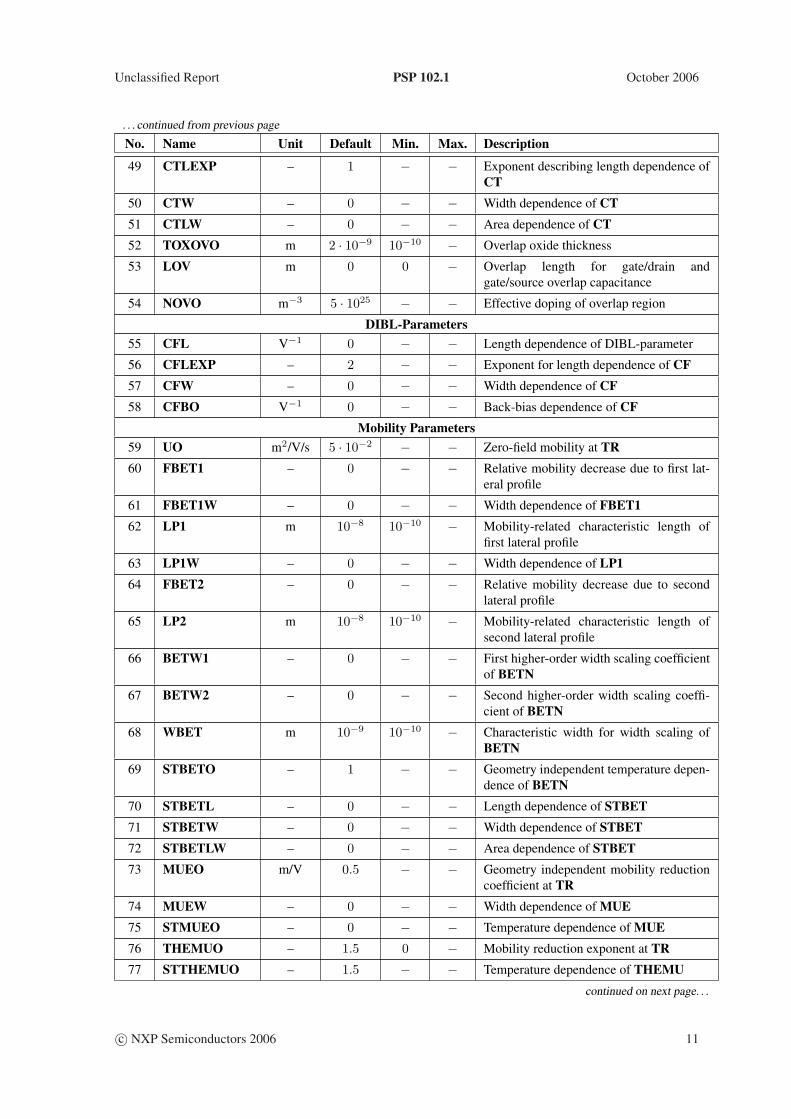
No. Name Unit Default Min. Max. Description
49 CTLEXP – 1 − − Exponent describing length dependence ofCT
50 CTW – 0 − − Width dependence of CT51 CTLW – 0 − − Area dependence of CT52 TOXOVO m 2 · 10−9 10−10 − Overlap oxide thickness
53 LOV m 0 0 − Overlap length for gate/drain andgate/source overlap capacitance
54 NOVO m−3 5 · 1025 − − Effective doping of overlap region
DIBL-Parameters55 CFL V−1 0 − − Length dependence of DIBL-parameter
56 CFLEXP – 2 − − Exponent for length dependence of CF57 CFW – 0 − − Width dependence of CF58 CFBO V−1 0 − − Back-bias dependence of CF
Mobility Parameters59 UO m2/V/s 5 · 10−2 − − Zero-field mobility at TR60 FBET1 – 0 − − Relative mobility decrease due to first lat-
eral profile
61 FBET1W – 0 − − Width dependence of FBET162 LP1 m 10−8 10−10 − Mobility-related characteristic length of
first lateral profile
63 LP1W – 0 − − Width dependence of LP164 FBET2 – 0 − − Relative mobility decrease due to second
lateral profile
65 LP2 m 10−8 10−10 − Mobility-related characteristic length ofsecond lateral profile
66 BETW1 – 0 − − First higher-order width scaling coefficientof BETN
67 BETW2 – 0 − − Second higher-order width scaling coeffi-cient of BETN
68 WBET m 10−9 10−10 − Characteristic width for width scaling ofBETN
69 STBETO – 1 − − Geometry independent temperature depen-dence of BETN
70 STBETL – 0 − − Length dependence of STBET71 STBETW – 0 − − Width dependence of STBET72 STBETLW – 0 − − Area dependence of STBET73 MUEO m/V 0.5 − − Geometry independent mobility reduction
coefficient at TR74 MUEW – 0 − − Width dependence of MUE75 STMUEO – 0 − − Temperature dependence of MUE76 THEMUO – 1.5 0 − Mobility reduction exponent at TR77 STTHEMUO – 1.5 − − Temperature dependence of THEMU
continued on next page. . .
c© NXP Semiconductors 2006 11
October 2006 PSP 102.1 Unclassified Report
. . . continued from previous page
No. Name Unit Default Min. Max. Description
78 CSO – 0 − − Geometry independent Coulomb scatteringparameter at TR
79 CSL – 0 − − Length dependence of CS80 CSLEXP – 0 − − Exponent for length dependence of CS81 CSW – 0 − − Width dependence of CS82 CSLW – 0 − − Area dependence of CS83 STCSO – 0 − − Temperature dependence of CS84 XCORO V−1 0 − − Geometry independent non-universality
parameter
85 XCORL – 0 − − Length dependence of XCOR86 XCORW – 0 − − Width dependence of XCOR87 XCORLW – 0 − − Area dependence of XCOR88 STXCORO – 0 − − Temperature dependence of XCOR89 FETAO – 1 − − Effective field parameter
Series Resistance Parameters90 RSW1 Ω 2500 − − Source/drain series resistance for channel
width WEN at TR91 RSW2 – 0 − − Higher-order width scaling of source/drain
series resistance
92 STRSO – 1 − − Temperature dependence of RS93 RSBO V−1 0 − − Back-bias dependence of RS94 RSGO V−1 0 − − Gate-bias dependence of RS
Velocity Saturation Parameters95 THESATO V−1 0 − − Geometry independent velocity saturation
parameter at TR96 THESATL V−1 0.05 − − Length dependence of THESAT97 THESATLEXP – 1 − − Exponent for length dependence of THE-
SAT98 THESATW – 0 − − Width dependence of THESAT99 THESATLW – 0 − − Area dependence THESAT
100 STTHESATO – 1 − − Geometry independent temperature depen-dence of THESAT
101 STTHESATL – 0 − − Length dependence of STTHESAT102 STTHESATW – 0 − − Width dependence of STTHESAT103 STTHESATLW – 0 − − Area dependence of STTHESAT104 THESATBO V−1 0 − − Back-bias dependence of THESAT105 THESATGO V−1 0 − − Gate-bias dependence of THESAT
Saturation Voltage Parameters106 AXO – 18 − − Geometry independent linear/saturation
transition factor
107 AXL – 0.4 0 − Length dependence of AXcontinued on next page. . .
12 c© NXP Semiconductors 2006
Unclassified Report PSP 102.1 October 2006
. . . continued from previous page
No. Name Unit Default Min. Max. Description
Channel Length Modulation (CLM) Parameters108 ALPL – 5 · 10−4 − − Length dependence of CLM pre-factor
ALP109 ALPLEXP – 1 − − Exponent for length dependence of ALP110 ALPW – 0 − − Width dependence of ALP111 ALP1L1 V 0 − − Length dependence of CLM enhancement
factor above threshold
112 ALP1LEXP – 0.5 − − Exponent describing the length depen-dence of ALP1
113 ALP1L2 – 0 0 − Second order length dependence of ALP1114 ALP1W – 0 − − Width dependence of ALP1115 ALP2L1 V 0 − − Length dependence of CLM enhancement
factor below threshold
116 ALP2LEXP – 0.5 − − Exponent describing the length depen-dence ALP2
117 ALP2L2 – 0 0 − Second order length dependence of ALP2118 ALP2W – 0 − − Width dependence of ALP2119 VPO V 0.05 − − CLM logarithmic dependence parameter
Impact Ionization (II) Parameters120 A1O – 1 − − Geometry independent part of impact-
ionization pre-factor A1121 A1L – 0 − − Length dependence of A1122 A1W – 0 − − Width dependence of A1123 A2O V 10 − − Impact-ionization exponent at TR124 STA2O V 0 − − Temperature dependence of A2125 A3O – 1.0 − − Geometry independent saturation-voltage
dependence of II
126 A3L – 0 − − Length dependence of A3127 A3W – 0 − − Width dependence of A3128 A4O V−
12 0 − − Geometry independent back-bias depen-
dence of II
129 A4L – 0 − − Length dependence of A4130 A4W – 0 − − Width dependence of A4
Gate Current Parameters131 GCOO – 0 − − Gate tunneling energy adjustment
132 IGINVLW A 0 − − Gate channel current pre-factor for a chan-nel area of WEN · LEN
133 IGOVW A 0 − − Gate overlap current pre-factor for a chan-nel width of WEN · LEN
134 STIGO – 2 − − Temperature dependence of gate current
135 GC2O – 0.375 − − Gate current slope factor
136 GC3O – 0.063 − − Gate current curvature factor
continued on next page. . .
c© NXP Semiconductors 2006 13
October 2006 PSP 102.1 Unclassified Report
. . . continued from previous page
No. Name Unit Default Min. Max. Description
137 CHIBO V 3.1 − − Tunneling barrier height
Gate-Induced Drain Leakage (GIDL) Parameters138 AGIDLW A/V3 0 − − Width dependence of GIDL pre-factor
139 BGIDLO V 41 − − GIDL probability factor at TR140 STBGIDLO V/K 0 − − Temperature dependence of BGIDL141 CGIDLO – 0 − − Back-bias dependence of GIDL
Charge Model Parameters142 CGBOVL F 0 − − Oxide capacitance for gate–bulk overlap
for an area of WEN · LEN
143 CFRW F 0 − − Outer fringe capacitance for a channelwidth of WEN
Noise Model Parameters144 FNTO – 1.0 − − Thermal noise coefficient
145 NFALW V−1/m4 8 · 1022 − − First coefficient of flicker noise for a chan-nel area of WEN · LEN
146 NFBLW V−1/m2 3 · 107 − − Second coefficient of flicker noise for achannel area of WEN · LEN
147 NFCLW V−1 0 − − Third coefficient of flicker noise for a chan-nel area of WEN · LEN
Other Parameters148 DTA K 0 − − Temperature offset w.r.t. ambient circuit
temperature
14 c© NXP Semiconductors 2006
Unclassified Report PSP 102.1 October 2006
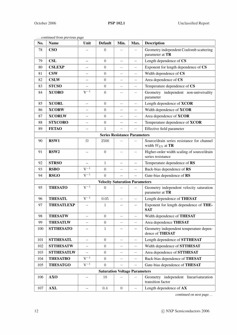
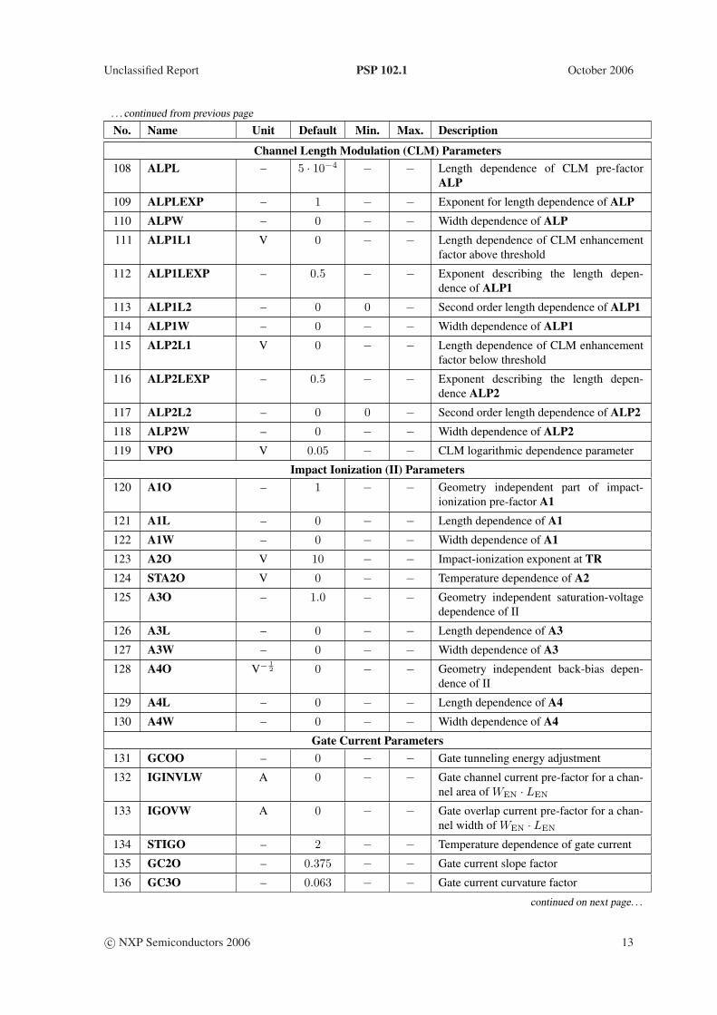
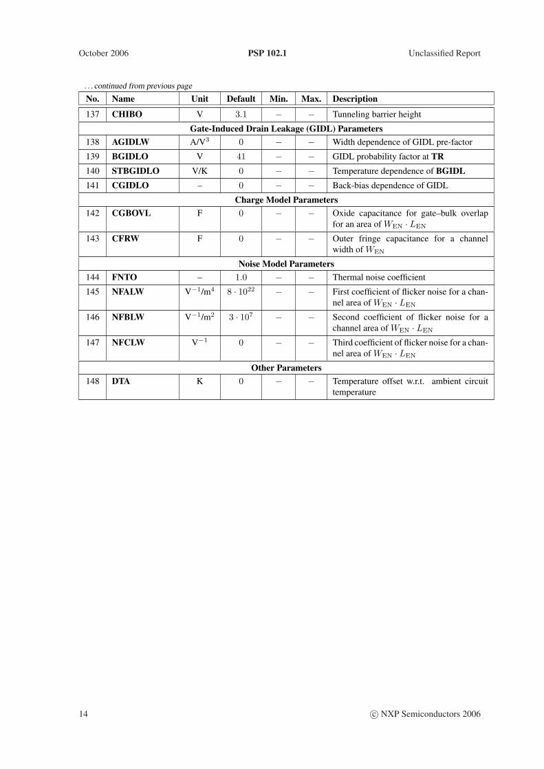
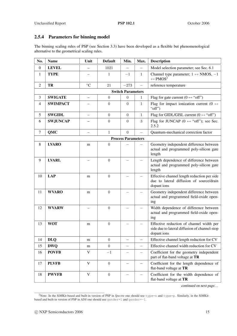
2.5.4 Parameters for binning model
The binning scaling rules of PSP (see Section 3.3) have been developed as a flexible but phenomenologicalalternative to the geometrical scaling rules.
No. Name Unit Default Min. Max. Description
0 LEVEL – 1021 − − Model selection parameter; see Sec. 6.1
1 TYPE – 1 −1 1 Channel type parameter; 1 ↔ NMOS, −1↔ PMOS2
2 TR C 21 −273 − reference temperature
Switch Parameters3 SWIGATE – 0 0 1 Flag for gate current (0 ↔ “off”)
4 SWIMPACT – 0 0 1 Flag for impact ionization current (0 ↔“off”)
5 SWGIDL – 0 0 1 Flag for GIDL/GISL current (0 ↔ “off”)
6 SWJUNCAP – 0 0 3 Flag for JUNCAP (0 ↔ “off”); see Sec.2.5.2
7 QMC – 1 0 − Quantum-mechanical correction factor
Process Parameters8 LVARO m 0 − − Geometry independent difference between
actual and programmed poly-silicon gatelength
9 LVARL – 0 − − Length dependence of difference betweenactual and programmed poly-silicon gatelength
10 LAP m 0 − − Effective channel length reduction per sidedue to lateral diffusion of source/draindopant ions
11 WVARO m 0 − − Geometry independent difference betweenactual and programmed field-oxide open-ing
12 WVARW – 0 − − Width dependence of difference betweenactual and programmed field-oxide open-ing
13 WOT m 0 − − Effective reduction of channel width perside due to lateral diffusion of channel-stopdopant ions
14 DLQ m 0 − − Effective channel length reduction for CV
15 DWQ m 0 − − Effective channel width reduction for CV
16 POVFB V −1 − − Coefficient for the geometry independentpart of flat-band voltage at TR
17 PLVFB V 0 − − Coefficient for the length dependence offlat-band voltage at TR
18 PWVFB V 0 − − Coefficient for the width dependence offlat-band voltage at TR
continued on next page. . .
2Note: In the SiMKit-based and built-in version of PSP in Spectre one should use type=n and type=p. Similarly, in the SiMKit-based and built-in version of PSP in ADS one should use gender=1 and gender=-1.
c© NXP Semiconductors 2006 15
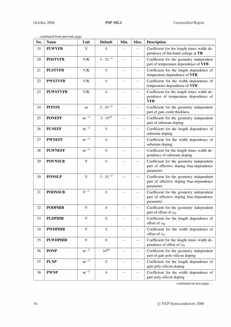
October 2006 PSP 102.1 Unclassified Report
. . . continued from previous page
No. Name Unit Default Min. Max. Description
19 PLWVFB V 0 − − Coefficient for the length times width de-pendence of flat-band voltage at TR
20 POSTVFB V/K 5 · 10−4 − − Coefficient for the geometry independentpart of temperature dependence of VFB
21 PLSTVFB V/K 0 − − Coefficient for the length dependence oftemperature dependence of VFB
22 PWSTVFB V/K 0 − − Coefficient for the width dependence oftemperature dependence of VFB
23 PLWSTVFB V/K 0 − − Coefficient for the length times width de-pendence of temperature dependence ofVFB
24 POTOX m 2 · 10−9 − − Coefficient for the geometry independentpart of gate oxide thickness
25 PONEFF m−3 5 · 1023 − − Coefficient for the geometry independentpart of substrate doping
26 PLNEFF m−3 0 − − Coefficient for the length dependence ofsubstrate doping
27 PWNEFF m−3 0 − − Coefficient for the width dependence ofsubstrate doping
28 PLWNEFF m−3 0 − − Coefficient for the length times width de-pendence of substrate doping
29 POVNSUB V 0 − − Coefficient for the geometry independentpart of effective doping bias-dependenceparameter
30 PONSLP V 5 · 10−2 − − Coefficient for the geometry independentpart of effective doping bias-dependenceparameter
31 PODNSUB V−1 0 − − Coefficient for the geometry independentpart of effective doping bias-dependenceparameter
32 PODPHIB V 0 − − Coefficient for the geometry independentpart of offset of φB
33 PLDPHIB V 0 − − Coefficient for the length dependence ofoffset of φB
34 PWDPHIB V 0 − − Coefficient for the width dependence ofoffset of φB
35 PLWDPHIB V 0 − − Coefficient for the length times width de-pendence of offset of φB
36 PONP m−3 1026 − − Coefficient for the geometry independentpart of gate poly-silicon doping
37 PLNP m−3 0 − − Coefficient for the length dependence ofgate poly-silicon doping
38 PWNP m−3 0 − − Coefficient for the width dependence ofgate poly-silicon doping
continued on next page. . .
16 c© NXP Semiconductors 2006
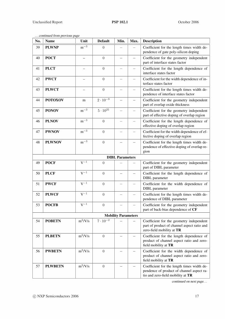
Unclassified Report PSP 102.1 October 2006
. . . continued from previous page
No. Name Unit Default Min. Max. Description
39 PLWNP m−3 0 − − Coefficient for the length times width de-pendence of gate poly-silicon doping
40 POCT – 0 − − Coefficient for the geometry independentpart of interface states factor
41 PLCT – 0 − − Coefficient for the length dependence ofinterface states factor
42 PWCT – 0 − − Coefficient for the width dependence of in-terface states factor
43 PLWCT – 0 − − Coefficient for the length times width de-pendence of interface states factor
44 POTOXOV m 2 · 10−9 − − Coefficient for the geometry independentpart of overlap oxide thickness
45 PONOV m−3 5 · 1025 − − Coefficient for the geometry independentpart of effective doping of overlap region
46 PLNOV m−3 0 − − Coefficient for the length dependence ofeffective doping of overlap region
47 PWNOV m−3 0 − − Coefficient for the width dependence of ef-fective doping of overlap region
48 PLWNOV m−3 0 − − Coefficient for the length times width de-pendence of effective doping of overlap re-gion
DIBL Parameters49 POCF V−1 0 − − Coefficient for the geometry independent
part of DIBL parameter
50 PLCF V−1 0 − − Coefficient for the length dependence ofDIBL parameter
51 PWCF V−1 0 − − Coefficient for the width dependence ofDIBL parameter
52 PLWCF V−1 0 − − Coefficient for the length times width de-pendence of DIBL parameter
53 POCFB V−1 0 − − Coefficient for the geometry independentpart of back-bias dependence of CF
Mobility Parameters54 POBETN m2/V/s 7 · 10−2 − − Coefficient for the geometry independent
part of product of channel aspect ratio andzero-field mobility at TR
55 PLBETN m2/V/s 0 − − Coefficient for the length dependence ofproduct of channel aspect ratio and zero-field mobility at TR
56 PWBETN m2/V/s 0 − − Coefficient for the width dependence ofproduct of channel aspect ratio and zero-field mobility at TR
57 PLWBETN m2/V/s 0 − − Coefficient for the length times width de-pendence of product of channel aspect ra-tio and zero-field mobility at TR
continued on next page. . .
c© NXP Semiconductors 2006 17
October 2006 PSP 102.1 Unclassified Report
. . . continued from previous page
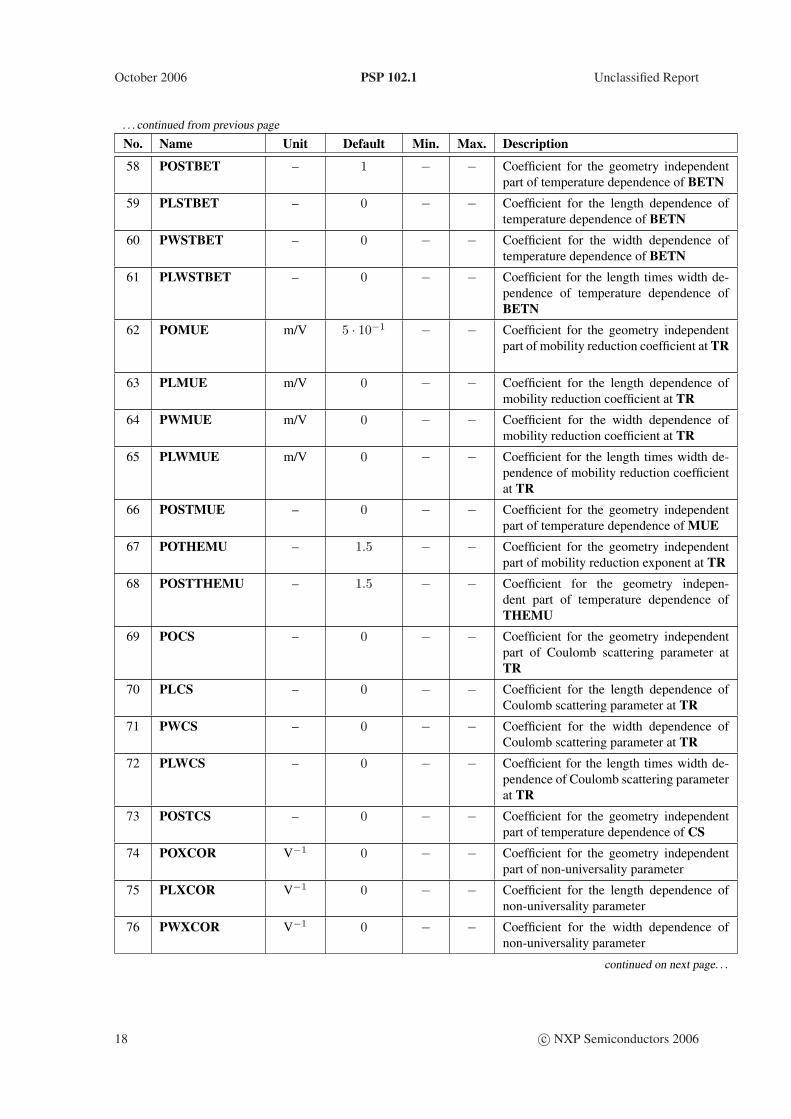
No. Name Unit Default Min. Max. Description
58 POSTBET – 1 − − Coefficient for the geometry independentpart of temperature dependence of BETN
59 PLSTBET – 0 − − Coefficient for the length dependence oftemperature dependence of BETN
60 PWSTBET – 0 − − Coefficient for the width dependence oftemperature dependence of BETN
61 PLWSTBET – 0 − − Coefficient for the length times width de-pendence of temperature dependence ofBETN
62 POMUE m/V 5 · 10−1 − − Coefficient for the geometry independentpart of mobility reduction coefficient at TR
63 PLMUE m/V 0 − − Coefficient for the length dependence ofmobility reduction coefficient at TR
64 PWMUE m/V 0 − − Coefficient for the width dependence ofmobility reduction coefficient at TR
65 PLWMUE m/V 0 − − Coefficient for the length times width de-pendence of mobility reduction coefficientat TR
66 POSTMUE – 0 − − Coefficient for the geometry independentpart of temperature dependence of MUE
67 POTHEMU – 1.5 − − Coefficient for the geometry independentpart of mobility reduction exponent at TR
68 POSTTHEMU – 1.5 − − Coefficient for the geometry indepen-dent part of temperature dependence ofTHEMU
69 POCS – 0 − − Coefficient for the geometry independentpart of Coulomb scattering parameter atTR
70 PLCS – 0 − − Coefficient for the length dependence ofCoulomb scattering parameter at TR
71 PWCS – 0 − − Coefficient for the width dependence ofCoulomb scattering parameter at TR
72 PLWCS – 0 − − Coefficient for the length times width de-pendence of Coulomb scattering parameterat TR
73 POSTCS – 0 − − Coefficient for the geometry independentpart of temperature dependence of CS
74 POXCOR V−1 0 − − Coefficient for the geometry independentpart of non-universality parameter
75 PLXCOR V−1 0 − − Coefficient for the length dependence ofnon-universality parameter
76 PWXCOR V−1 0 − − Coefficient for the width dependence ofnon-universality parameter
continued on next page. . .
18 c© NXP Semiconductors 2006
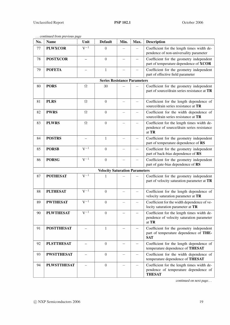
Unclassified Report PSP 102.1 October 2006
. . . continued from previous page
No. Name Unit Default Min. Max. Description
77 PLWXCOR V−1 0 − − Coefficient for the length times width de-pendence of non-universality parameter
78 POSTXCOR – 0 − − Coefficient for the geometry independentpart of temperature dependence of XCOR
79 POFETA – 1 − − Coefficient for the geometry independentpart of effective field parameter
Series Resistance Parameters80 PORS Ω 30 − − Coefficient for the geometry independent
part of source/drain series resistance at TR
81 PLRS Ω 0 − − Coefficient for the length dependence ofsource/drain series resistance at TR
82 PWRS Ω 0 − − Coefficient for the width dependence ofsource/drain series resistance at TR
83 PLWRS Ω 0 − − Coefficient for the length times width de-pendence of source/drain series resistanceat TR
84 POSTRS – 1 − − Coefficient for the geometry independentpart of temperature dependence of RS
85 PORSB V−1 0 − − Coefficient for the geometry independentpart of back-bias dependence of RS
86 PORSG V−1 0 − − Coefficient for the geometry independentpart of gate-bias dependence of RS
Velocity Saturation Parameters87 POTHESAT V−1 1 − − Coefficient for the geometry independent
part of velocity saturation parameter at TR
88 PLTHESAT V−1 0 − − Coefficient for the length dependence ofvelocity saturation parameter at TR
89 PWTHESAT V−1 0 − − Coefficient for the width dependence of ve-locity saturation parameter at TR
90 PLWTHESAT V−1 0 − − Coefficient for the length times width de-pendence of velocity saturation parameterat TR
91 POSTTHESAT – 1 − − Coefficient for the geometry independentpart of temperature dependence of THE-SAT
92 PLSTTHESAT – 0 − − Coefficient for the length dependence oftemperature dependence of THESAT
93 PWSTTHESAT – 0 − − Coefficient for the width dependence oftemperature dependence of THESAT
94 PLWSTTHESAT – 0 − − Coefficient for the length times width de-pendence of temperature dependence ofTHESAT
continued on next page. . .
c© NXP Semiconductors 2006 19
October 2006 PSP 102.1 Unclassified Report
. . . continued from previous page
No. Name Unit Default Min. Max. Description
95 POTHESATB V−1 0 − − Coefficient for the geometry independentpart of back-bias dependence of velocitysaturation
96 PLTHESATB V−1 0 − − Coefficient for the length dependence ofback-bias dependence of velocity satura-tion
97 PWTHESATB V−1 0 − − Coefficient for the width dependence ofback-bias dependence of velocity satura-tion
98 PLWTHESATB V−1 0 − − Coefficient for the length times width de-pendence of back-bias dependence of ve-locity saturation
99 POTHESATG V−1 0 − − Coefficient for the geometry independentpart of gate-bias dependence of velocitysaturation
100 PLTHESATG V−1 0 − − Coefficient for the length dependence ofgate-bias dependence of velocity saturation
101 PWTHESATG V−1 0 − − Coefficient for the width dependence ofgate-bias dependence of velocity saturation
102 PLWTHESATG V−1 0 − − Coefficient for the length times width de-pendence of gate-bias dependence of ve-locity saturation
Saturation Voltage Parameters103 POAX – 3 − − Coefficient for the geometry independent
part of linear/saturation transition factor
104 PLAX – 0 − − Coefficient for the length dependence oflinear/saturation transition factor
105 PWAX – 0 − − Coefficient for the width dependence oflinear/saturation transition factor
106 PLWAX – 0 − − Coefficient for the length times widthdependence of linear/saturation transitionfactor
Channel Length Modulation (CLM) Parameters107 POALP – 10−2 − − Coefficient for the geometry independent
part of CLM pre-factor
108 PLALP – 0 − − Coefficient for the length dependence ofCLM pre-factor
109 PWALP – 0 − − Coefficient for the width dependence ofCLM pre-factor
110 PLWALP – 0 − − Coefficient for the length times width de-pendence of CLM pre-factor
111 POALP1 V 0 − − Coefficient for the geometry independentpart of CLM enhancement factor abovethreshold
continued on next page. . .
20 c© NXP Semiconductors 2006
Unclassified Report PSP 102.1 October 2006
. . . continued from previous page
No. Name Unit Default Min. Max. Description
112 PLALP1 V 0 − − Coefficient for the length dependence ofCLM enhancement factor above threshold
113 PWALP1 V 0 − − Coefficient for the width dependence ofCLM enhancement factor above threshold
114 PLWALP1 V 0 − − Coefficient for the length times widthdependence of CLM enhancement factorabove threshold
115 POALP2 V−1 0 − − Coefficient for the geometry independentpart of CLM enhancement factor belowthreshold
116 PLALP2 V−1 0 − − Coefficient for the length dependence ofCLM enhancement factor below threshold
117 PWALP2 V−1 0 − − Coefficient for the width dependence ofCLM enhancement factor below threshold
118 PLWALP2 V−1 0 − − Coefficient for the length times width de-pendence of CLM enhancement factor be-low threshold
119 POVP V 5 · 10−2 − − Coefficient for the geometry independentpart of CLM logarithmic dependence para-meter
Impact Ionization (II) Parameters120 POA1 – 1 − − Coefficient for the geometry independent
part of impact-ionization pre-factor
121 PLA1 – 0 − − Coefficient for the length dependence ofimpact-ionization pre-factor
122 PWA1 – 0 − − Coefficient for the width dependence ofimpact-ionization pre-factor
123 PLWA1 – 0 − − Coefficient for the length times width de-pendence of impact-ionization pre-factor
124 POA2 V 10 − − Coefficient for the geometry independentpart of impact-ionization exponent at TR
125 POSTA2 V 0 − − Coefficient for the geometry independentpart of temperature dependence of A2
126 POA3 – 1 − − Coefficient for the geometry independentpart of saturation-voltage dependence of II
127 PLA3 – 0 − − Coefficient for the length dependence ofsaturation-voltage dependence of II
128 PWA3 – 0 − − Coefficient for the width dependence ofsaturation-voltage dependence of II
129 PLWA3 – 0 − − Coefficient for the length times widthdependence of saturation-voltage depen-dence of II
130 POA4 V−0.5 0 − − Coefficient for the geometry independentpart of back-bias dependence of II
continued on next page. . .
c© NXP Semiconductors 2006 21
October 2006 PSP 102.1 Unclassified Report
. . . continued from previous page
No. Name Unit Default Min. Max. Description
131 PLA4 V−0.5 0 − − Coefficient for the length dependence ofback-bias dependence of II
132 PWA4 V−0.5 0 − − Coefficient for the width dependence ofback-bias dependence of II
133 PLWA4 V−0.5 0 − − Coefficient for the length times width de-pendence of back-bias dependence of II
Gate Current Parameters134 POGCO – 0 − − Coefficient for the geometry independent
part of gate tunneling energy adjustment
135 POIGINV A 0 − − Coefficient for the geometry independentpart of gate channel current pre-factor
136 PLIGINV A 0 − − Coefficient for the length dependence ofgate channel current pre-factor
137 PWIGINV A 0 − − Coefficient for the width dependence ofgate channel current pre-factor
138 PLWIGINV A 0 − − Coefficient for the length times width de-pendence of gate channel current pre-factor
139 POIGOV A 0 − − Coefficient for the geometry independentpart of gate overlap current pre-factor
140 PLIGOV A 0 − − Coefficient for the length dependence ofgate overlap current pre-factor
141 PWIGOV A 0 − − Coefficient for the width dependence ofgate overlap current pre-factor
142 PLWIGOV A 0 − − Coefficient for the length times width de-pendence of gate overlap current pre-factor
143 POSTIG – 2 − − Coefficient for the geometry independentpart of temperature dependence of gatecurrent
144 POGC2 – 3.75 · 10−1 − − Coefficient for the geometry independentpart of gate current slope factor
145 POGC3 – 6.3 · 10−2 − − Coefficient for the geometry independentpart of gate current curvature factor
146 POCHIB V 3.1 − − Coefficient for the geometry independentpart of tunneling barrier height
Gate-Induced Drain Leakage (GIDL) Parameters147 POAGIDL A/V3 0 − − Coefficient for the geometry independent
part of GIDL pre-factor
148 PLAGIDL A/V3 0 − − Coefficient for the length dependence ofGIDL pre-factor
149 PWAGIDL A/V3 0 − − Coefficient for the width dependence ofGIDL pre-factor
150 PLWAGIDL A/V3 0 − − Coefficient for the length times width de-pendence of GIDL pre-factor
continued on next page. . .
22 c© NXP Semiconductors 2006
Unclassified Report PSP 102.1 October 2006
. . . continued from previous page
No. Name Unit Default Min. Max. Description
151 POBGIDL V 41 − − Coefficient for the geometry independentpart of GIDL probability factor at TR
152 POSTBGIDL V/K 0 − − Coefficient for the geometry independentpart of temperature dependence of BGIDL
153 POCGIDL – 0 − − Coefficient for the geometry independentpart of back-bias dependence of GIDL
Charge Model Parameters154 POCOX F 10−14 − − Coefficient for the geometry independent
part of oxide capacitance for intrinsicchannel
155 PLCOX F 0 − − Coefficient for the length dependence ofoxide capacitance for intrinsic channel
156 PWCOX F 0 − − Coefficient for the width dependence ofoxide capacitance for intrinsic channel
157 PLWCOX F 0 − − Coefficient for the length times width de-pendence of oxide capacitance for intrinsicchannel
158 POCGOV F 10−15 − − Coefficient for the geometry indepen-dent part of oxide capacitance for gate-drain/source overlap
159 PLCGOV F 0 − − Coefficient for the length dependence ofoxide capacitance for gate-drain/sourceoverlap
160 PWCGOV F 0 − − Coefficient for the width dependence ofoxide capacitance for gate-drain/sourceoverlap
161 PLWCGOV F 0 − − Coefficient for the length times width de-pendence of oxide capacitance for gate-drain/source overlap
162 POCGBOV F 0 − − Coefficient for the geometry independentpart of oxide capacitance for gate-bulkoverlap
163 PLCGBOV F 0 − − Coefficient for the length dependence ofoxide capacitance for gate-bulk overlap
164 PWCGBOV F 0 − − Coefficient for the width dependence ofoxide capacitance for gate-bulk overlap
165 PLWCGBOV F 0 − − Coefficient for the length times width de-pendence of oxide capacitance for gate-bulk overlap
166 POCFR F 0 − − Coefficient for the geometry independentpart of outer fringe capacitance
167 PLCFR F 0 − − Coefficient for the length dependence ofouter fringe capacitance
168 PWCFR F 0 − − Coefficient for the width dependence ofouter fringe capacitance
continued on next page. . .
c© NXP Semiconductors 2006 23
October 2006 PSP 102.1 Unclassified Report
. . . continued from previous page
No. Name Unit Default Min. Max. Description
169 PLWCFR F 0 − − Coefficient for the length times width de-pendence of outer fringe capacitance
Noise Model Parameters170 POFNT – 1 − − Coefficient for the geometry independent
part of thermal noise coefficient
171 PONFA V−1/m4 8 · 1022 − − Coefficient for the geometry independentpart of first coefficient of flicker noise
172 PLNFA V−1/m4 0 − − Coefficient for the length dependence offirst coefficient of flicker noise
173 PWNFA V−1/m4 0 − − Coefficient for the width dependence offirst coefficient of flicker noise
174 PLWNFA V−1/m4 0 − − Coefficient for the length times width de-pendence of first coefficient of flicker noise
175 PONFB V−1/m2 3 · 107 − − Coefficient for the geometry independentpart of second coefficient of flicker noise
176 PLNFB V−1/m2 0 − − Coefficient for the length dependence ofsecond coefficient of flicker noise
177 PWNFB V−1/m2 0 − − Coefficient for the width dependence ofsecond coefficient of flicker noise
178 PLWNFB V−1/m2 0 − − Coefficient for the length times width de-pendence of second coefficient of flickernoise
179 PONFC V−1 0 − − Coefficient for the geometry independentpart of third coefficient of flicker noise
180 PLNFC V−1 0 − − Coefficient for the length dependence ofthird coefficient of flicker noise
181 PWNFC V−1 0 − − Coefficient for the width dependence ofthird coefficient of flicker noise
182 PLWNFC V−1 0 − − Coefficient for the length times width de-pendence of third coefficient of flickernoise
Other Parameters183 DTA K 0 − − temperature offset w.r.t. ambient circuit
temperature
24 c© NXP Semiconductors 2006
Unclassified Report PSP 102.1 October 2006
2.5.5 Parameters for stress model
The stress model of BSIM4.4.0 has been adopted in PSP with as little modifications as possible. Parameternames have been copied, but they have been subjected to PSP conventions by replacing every zero by an‘O’. Moreover, the parameters STK2 and LODK2 are not available in PSP. Except for these changes, stressparameters determined for BSIM can be directly applied in PSP.
The parameters in this section are part of PSP’s global parameter set (both geometrical and binning).
No. Name Unit Default Min. Max. Description
0 SAREF m 10−6 10−9 − Reference distance betweenOD edge to Poly from oneside
1 SBREF m 10−6 10−9 − Reference distance betweenOD edge to Poly from otherside
2 WLOD m 0 − − Width parameter
3 KUO m 0 − − Mobility degrada-tion/enhancement coef-ficient
4 KVSAT m 0 −1 1 Saturation velocity degrada-tion/enhancement parameter
5 TKUO – 0 − − Temperature coefficient ofKUO
6 LKUO mLLODKUO 0 − − Length dependence of KUO
7 WKUO mWLODKUO 0 − − Width dependence of KUO8 PKUO mLLODKUO+WLODKUO 0 − − Cross-term dependence of
KUO9 LLODKUO – 0 0 − Length parameter for mobil-
ity stress effect
10 WLODKUO – 0 0 − Width parameter for mobil-ity stress effect
11 KVTHO Vm 0 − − Threshold shift parameter
12 LKVTHO mLLODVTH 0 − − Length dependence ofKVTHO
13 WKVTHO mWLODVTH 0 − − Width dependence ofKVTHO
14 PKVTHO mLLODVTH+WLODVTH 0 − − Cross-term dependence ofKVTHO
15 LLODVTH – 0 0 − Length parameter for thres-hold voltage stress effect
16 WLODVTH – 0 0 − Width parameter for thres-hold voltage stress effect
17 STETAO m 0 − − ETAO shift factor related tothreshold voltage change
continued on next page. . .
c© NXP Semiconductors 2006 25
October 2006 PSP 102.1 Unclassified Report
. . . continued from previous page
No. Name Unit Default Min. Max. Description
18 LODETAO – 1 0 − ETAO shift modificationfactor
26 c© NXP Semiconductors 2006
Unclassified Report PSP 102.1 October 2006
2.5.6 Parameters for local model
The set of local parameters valid for an individual transistor with a specific channel width and length are givenin the table below. Since the local parameter set is valid for one device with a specific geometry, it does notcontain the channel length and width as instance parameters.
No. Name Unit Default Min. Max. Description
0 LEVEL – 102 − − Model selection parameter; see Sec. 6.1
1 TYPE – 1 −1 1 Channel type parameter; 1 ↔ NMOS, −1↔ PMOS3
2 TR C 21 −273 − Reference temperature
Switch Parameters3 SWIGATE – 0 0 1 Flag for gate current (0 ↔ “off”)
4 SWIMPACT – 0 0 1 Flag for impact ionization current (0 ↔“off”)
5 SWGIDL – 0 0 1 Flag for GIDL/GISL current (0 ↔ “off”)
6 SWJUNCAP – 0 0 3 Flag for JUNCAP (0 ↔ “off”); seeSec. 2.5.2
7 QMC – 1 0 − Quantum-mechanical correction factor
Process Parameters8 VFB V −1 − − Flat-band voltage at TR9 STVFB V/K 5 · 10−4 − − Temperature dependence of VFB
10 TOX m 2 · 10−9 10−10 − Gate oxide thickness
11 NEFF m−3 5 · 1023 1020 1026 Substrate doping
12 VNSUB V 0 − − Effective doping bias-dependence parame-ter
13 NSLP V 0.05 10−3 − Effective doping bias-dependence parame-ter
14 DNSUB V−1 0 0 1 Effective doping bias-dependence parame-ter
15 DPHIB V 0 − − Offset of ϕB
16 NP m−3 1026 0 − Gate poly-silicon doping
17 CT – 0 0 − Interface states factor
18 TOXOV m 2 · 10−9 10−10 − Overlap oxide thickness
19 NOV m−3 5 · 1025 1020 1027 Effective doping of overlap region
DIBL Parameters20 CF V−1 0 0 − DIBL parameter
21 CFB V−1 0 0 1 Back-bias dependence of CFMobility Parameters
22 BETN m2/V/s 7 · 10−2 0 − Product of channel aspect ratio and zero-field mobility at TR
23 STBET – 1 − − Temperature dependence of BETN24 MUE m/V 0.5 0 − Mobility reduction coefficient at TR
continued on next page. . .
3Note: In the SiMKit-based and built-in version of PSP in Spectre one should use type=n and type=p. Similarly, in the SiMKit-based and built-in version of PSP in ADS one should use gender=1 and gender=-1.
c© NXP Semiconductors 2006 27
October 2006 PSP 102.1 Unclassified Report
. . . continued from previous page
No. Name Unit Default Min. Max. Description
25 STMUE – 0 − − Temperature dependence of MUE26 THEMU – 1.5 0 − Mobility reduction exponent at TR27 STTHEMU – 1.5 − − Temperature dependence of THEMU28 CS – 0 0 − Coulomb scattering parameter at TR29 STCS – 0 − − Temperature dependence of CS30 XCOR V−1 0 0 − Non-universality parameter
31 STXCOR – 0 − − Temperature dependence of XCOR32 FETA – 1 0 − Effective field parameter
Series Resistance Parameters33 RS Ω 30 0 − Source/drain series resistance at TR34 STRS – 1 − − Temperature dependence of RS35 RSB V−1 0 −0.5 1 Back-bias dependence of RS36 RSG V−1 0 −0.5 − Gate-bias dependence of RS
Velocity Saturation Parameters37 THESAT V−1 1 0 − Velocity saturation parameter at TR38 STTHESAT – 1 − − Temperature dependence of THESAT39 THESATB V−1 0 −0.5 1 Back-bias dependence of velocity satura-
tion
40 THESATG V−1 0 −0.5 − Gate-bias dependence of velocity satura-tion
Saturation Voltage Parameter41 AX - 3 2 − Linear/saturation transition factor
Channel Length Modulation (CLM) Parameters42 ALP – 0.01 0 − CLM pre-factor
43 ALP1 V 0 0 − CLM enhancement factor above threshold
44 ALP2 V−1 0 0 − CLM enhancement factor below threshold
45 VP V 0.05 10−10 − CLM logarithmic dependence parameter
Impact Ionization (II) Parameters46 A1 – 1 0 − Impact-ionization pre-factor
47 A2 V 10 0 − Impact-ionization exponent at TR48 STA2 V 0 − − Temperature dependence of A249 A3 – 1 0 − Saturation-voltage dependence of II
50 A4 V−12 0 0 − Back-bias dependence of II
Gate Current Parameters51 GCO – 0 −10 10 Gate tunnelling energy adjustment
52 IGINV A 0 0 − Gate channel current pre-factor
53 IGOV A 0 0 − Gate overlap current pre-factor
54 STIG – 2 − − Temperature dependence of gate current
55 GC2 – 0.375 0 10 Gate current slope factor
56 GC3 – 0.063 −2 2 Gate current curvature factor
continued on next page. . .
28 c© NXP Semiconductors 2006
Unclassified Report PSP 102.1 October 2006
. . . continued from previous page
No. Name Unit Default Min. Max. Description
57 CHIB V 3.1 1 − Tunnelling barrier height
Gate-Induced Drain Leakage (GIDL) Parameters58 AGIDL A/V3 0 0 − GIDL pre-factor
59 BGIDL V 41 0 − GIDL probability factor at TR60 STBGIDL V/K 0 − − Temperature dependence of BGIDL61 CGIDL – 0 − − Back-bias dependence of GIDL
Charge Model Parameters62 COX F 10−14 0 − Oxide capacitance for intrinsic channel
63 CGOV F 10−15 0 − Oxide capacitance for gate–drain/sourceoverlap
64 CGBOV F 0 0 − Oxide capacitance for gate–bulk overlap
65 CFR F 0 0 − Outer fringe capacitance
Noise Model Parameters66 FNT – 1.0 0 − Thermal noise coefficient
67 NFA V−1/m4 8 · 1022 0 − First coefficient of flicker noise
68 NFB V−1/m2 3 · 107 0 − Second coefficient of flicker noise
69 NFC V−1 0 0 − Third coefficient of flicker noise
Other Parameters70 DTA K 0 − − Temperature offset w.r.t. ambient circuit
temperature
c© NXP Semiconductors 2006 29
October 2006 PSP 102.1 Unclassified Report
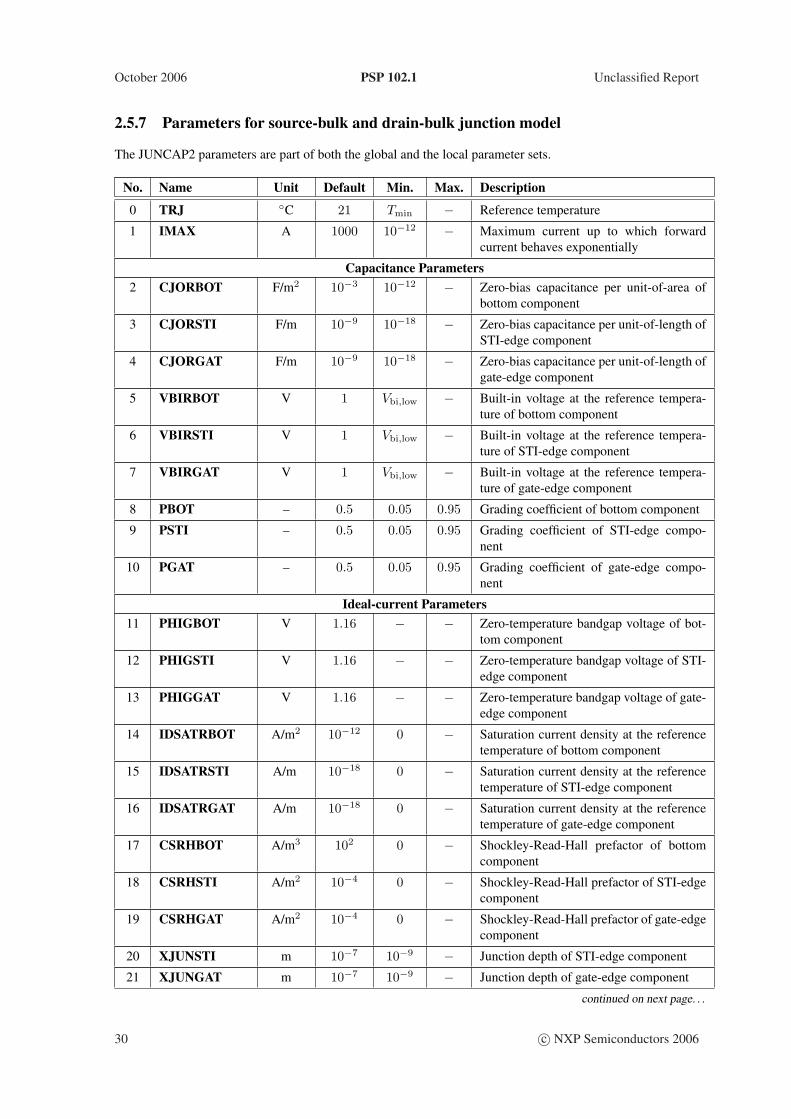
2.5.7 Parameters for source-bulk and drain-bulk junction model
The JUNCAP2 parameters are part of both the global and the local parameter sets.
No. Name Unit Default Min. Max. Description
0 TRJ C 21 Tmin − Reference temperature
1 IMAX A 1000 10−12 − Maximum current up to which forwardcurrent behaves exponentially
Capacitance Parameters2 CJORBOT F/m2 10−3 10−12 − Zero-bias capacitance per unit-of-area of
bottom component
3 CJORSTI F/m 10−9 10−18 − Zero-bias capacitance per unit-of-length ofSTI-edge component
4 CJORGAT F/m 10−9 10−18 − Zero-bias capacitance per unit-of-length ofgate-edge component
5 VBIRBOT V 1 Vbi,low − Built-in voltage at the reference tempera-ture of bottom component
6 VBIRSTI V 1 Vbi,low − Built-in voltage at the reference tempera-ture of STI-edge component
7 VBIRGAT V 1 Vbi,low − Built-in voltage at the reference tempera-ture of gate-edge component
8 PBOT – 0.5 0.05 0.95 Grading coefficient of bottom component
9 PSTI – 0.5 0.05 0.95 Grading coefficient of STI-edge compo-nent
10 PGAT – 0.5 0.05 0.95 Grading coefficient of gate-edge compo-nent
Ideal-current Parameters11 PHIGBOT V 1.16 − − Zero-temperature bandgap voltage of bot-
tom component
12 PHIGSTI V 1.16 − − Zero-temperature bandgap voltage of STI-edge component
13 PHIGGAT V 1.16 − − Zero-temperature bandgap voltage of gate-edge component
14 IDSATRBOT A/m2 10−12 0 − Saturation current density at the referencetemperature of bottom component
15 IDSATRSTI A/m 10−18 0 − Saturation current density at the referencetemperature of STI-edge component
16 IDSATRGAT A/m 10−18 0 − Saturation current density at the referencetemperature of gate-edge component
17 CSRHBOT A/m3 102 0 − Shockley-Read-Hall prefactor of bottomcomponent
18 CSRHSTI A/m2 10−4 0 − Shockley-Read-Hall prefactor of STI-edgecomponent
19 CSRHGAT A/m2 10−4 0 − Shockley-Read-Hall prefactor of gate-edgecomponent
20 XJUNSTI m 10−7 10−9 − Junction depth of STI-edge component
21 XJUNGAT m 10−7 10−9 − Junction depth of gate-edge component
continued on next page. . .
30 c© NXP Semiconductors 2006
Unclassified Report PSP 102.1 October 2006
. . . continued from previous page
No. Name Unit Default Min. Max. Description
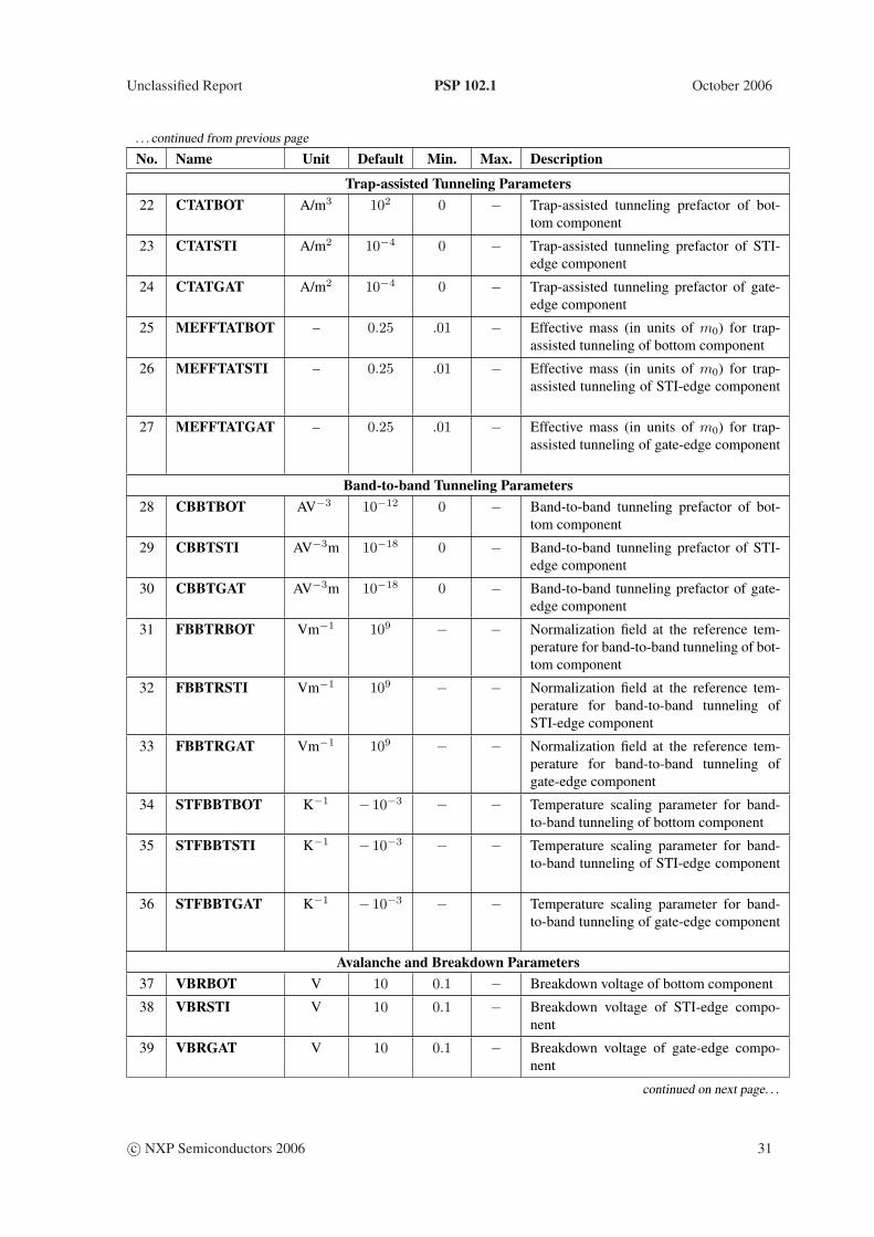
Trap-assisted Tunneling Parameters22 CTATBOT A/m3 102 0 − Trap-assisted tunneling prefactor of bot-
tom component
23 CTATSTI A/m2 10−4 0 − Trap-assisted tunneling prefactor of STI-edge component
24 CTATGAT A/m2 10−4 0 − Trap-assisted tunneling prefactor of gate-edge component
25 MEFFTATBOT – 0.25 .01 − Effective mass (in units of m0) for trap-assisted tunneling of bottom component
26 MEFFTATSTI – 0.25 .01 − Effective mass (in units of m0) for trap-assisted tunneling of STI-edge component
27 MEFFTATGAT – 0.25 .01 − Effective mass (in units of m0) for trap-assisted tunneling of gate-edge component
Band-to-band Tunneling Parameters28 CBBTBOT AV−3 10−12 0 − Band-to-band tunneling prefactor of bot-
tom component
29 CBBTSTI AV−3m 10−18 0 − Band-to-band tunneling prefactor of STI-edge component
30 CBBTGAT AV−3m 10−18 0 − Band-to-band tunneling prefactor of gate-edge component
31 FBBTRBOT Vm−1 109 − − Normalization field at the reference tem-perature for band-to-band tunneling of bot-tom component
32 FBBTRSTI Vm−1 109 − − Normalization field at the reference tem-perature for band-to-band tunneling ofSTI-edge component
33 FBBTRGAT Vm−1 109 − − Normalization field at the reference tem-perature for band-to-band tunneling ofgate-edge component
34 STFBBTBOT K−1 − 10−3 − − Temperature scaling parameter for band-to-band tunneling of bottom component
35 STFBBTSTI K−1 − 10−3 − − Temperature scaling parameter for band-to-band tunneling of STI-edge component
36 STFBBTGAT K−1 − 10−3 − − Temperature scaling parameter for band-to-band tunneling of gate-edge component
Avalanche and Breakdown Parameters37 VBRBOT V 10 0.1 − Breakdown voltage of bottom component
38 VBRSTI V 10 0.1 − Breakdown voltage of STI-edge compo-nent
39 VBRGAT V 10 0.1 − Breakdown voltage of gate-edge compo-nent
continued on next page. . .
c© NXP Semiconductors 2006 31
October 2006 PSP 102.1 Unclassified Report
. . . continued from previous page
No. Name Unit Default Min. Max. Description
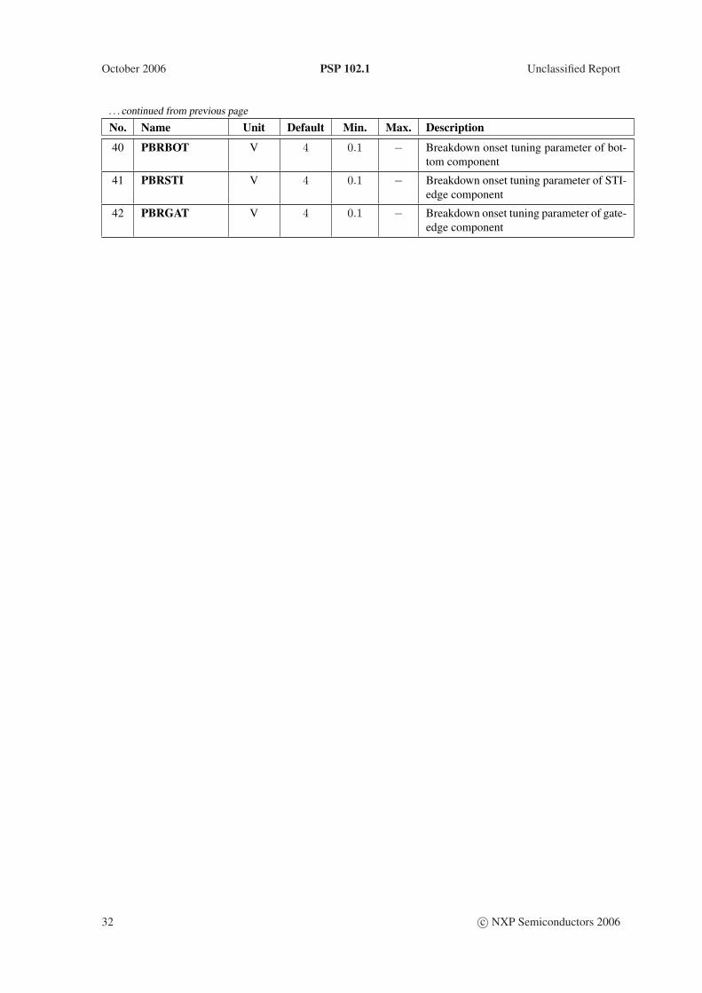
40 PBRBOT V 4 0.1 − Breakdown onset tuning parameter of bot-tom component
41 PBRSTI V 4 0.1 − Breakdown onset tuning parameter of STI-edge component
42 PBRGAT V 4 0.1 − Breakdown onset tuning parameter of gate-edge component
32 c© NXP Semiconductors 2006
Unclassified Report PSP 102.1 October 2006
Section 3
Geometry and Stress dependence
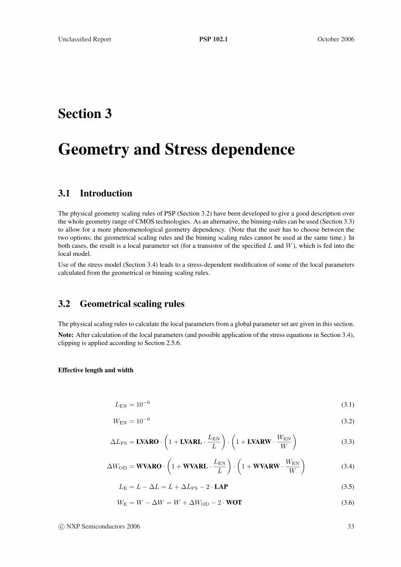
3.1 Introduction
The physical geometry scaling rules of PSP (Section 3.2) have been developed to give a good description overthe whole geometry range of CMOS technologies. As an alternative, the binning-rules can be used (Section 3.3)to allow for a more phenomenological geometry dependency. (Note that the user has to choose between thetwo options; the geometrical scaling rules and the binning scaling rules cannot be used at the same time.) Inboth cases, the result is a local parameter set (for a transistor of the specified L and W ), which is fed into thelocal model.
Use of the stress model (Section 3.4) leads to a stress-dependent modification of some of the local parameterscalculated from the geometrical or binning scaling rules.
3.2 Geometrical scaling rules
The physical scaling rules to calculate the local parameters from a global parameter set are given in this section.
Note: After calculation of the local parameters (and possible application of the stress equations in Section 3.4),clipping is applied according to Section 2.5.6.
Effective length and width
LEN = 10−6 (3.1)
WEN = 10−6 (3.2)
∆LPS = LVARO ·(
1 + LVARL · LEN
L
)·(
1 + LVARW · WEN
W
)(3.3)
∆WOD = WVARO ·(
1 + WVARL · LEN
L
)·(
1 + WVARW · WEN
W
)(3.4)
LE = L−∆L = L + ∆LPS − 2 · LAP (3.5)
WE = W −∆W = W + ∆WOD − 2 ·WOT (3.6)
c© NXP Semiconductors 2006 33
October 2006 PSP 102.1 Unclassified Report
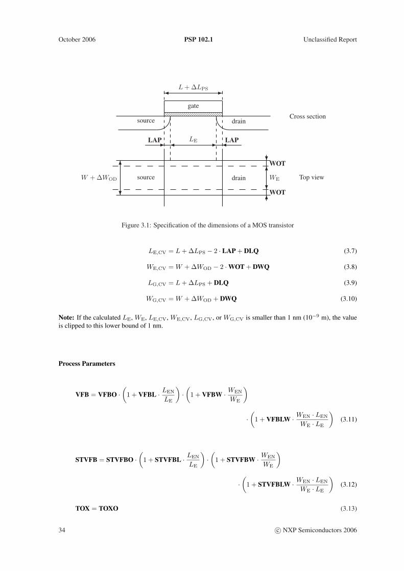
Cross section
gatep p p p p p p p p p p p p p p p p p p p p p p p p p p p p pp p p p p p p p p p p p p p p p p p p p p p p p p p p p pp p p p p p p p p p p p p p p p p p p p p p p p p p p p p p
!source
"drain
Top viewsource drain
-¾ L + ∆LPS
-¾ LE
6
?
W + ∆WOD
6
?WE
6WOT
?WOT
- ¾LAP LAP
Figure 3.1: Specification of the dimensions of a MOS transistor
LE,CV = L + ∆LPS − 2 · LAP + DLQ (3.7)
WE,CV = W + ∆WOD − 2 ·WOT + DWQ (3.8)
LG,CV = L + ∆LPS + DLQ (3.9)
WG,CV = W + ∆WOD + DWQ (3.10)
Note: If the calculated LE, WE, LE,CV, WE,CV, LG,CV, or WG,CV is smaller than 1 nm (10−9 m), the valueis clipped to this lower bound of 1 nm.
Process Parameters
VFB = VFBO ·(
1 + VFBL · LEN
LE
)·(
1 + VFBW · WEN
WE
)
·(
1 + VFBLW · WEN · LEN
WE · LE
)(3.11)
STVFB = STVFBO ·(
1 + STVFBL · LEN
LE
)·(
1 + STVFBW · WEN
WE
)
·(
1 + STVFBLW · WEN · LEN
WE · LE
)(3.12)
TOX = TOXO (3.13)
34 c© NXP Semiconductors 2006
Unclassified Report PSP 102.1 October 2006
Nsub0,eff = NSUBO ·MAX([
1 + NSUBW · WEN
WE· ln
(1 +
WE
WSEG
)], 10−3
)(3.14)
Npck,eff = NPCK ·MAX([
1 + NPCKW · WEN
WE· ln
(1 +
WE
WSEGP
)], 10−3
)(3.15)
Lpck,eff = LPCK ·MAX([
1 + LPCKW · WEN
WE· ln
(1 +
WE
WSEGP
)], 10−3
)(3.16)
a = 7.5 · 1010 (3.17)
b =√
Nsub0,eff + 0.5 ·Npck,eff −√
Nsub0,eff (3.18)
Nsub =
Nsub0,eff + Npck,eff ·[2− LE
Lpck,eff
]for LE < Lpck,eff
Nsub0,eff + Npck,eff · Lpck,eff
LEfor Lpck,eff ≤ LE ≤ 2 · Lpck,eff
[√
Nsub0,eff +
a · ln(
1 + 2 · Lpck,eff
LE·[exp
(b
a
)− 1
])]2
for LE > 2 · Lpck,eff
(3.19)
NEFF = Nsub ·(
1− FOL1 · LEN
LE− FOL2 ·
[LEN
LE
]2)
(3.20)
VNSUB = VNSUBO (3.21)
NSLP = NSLPO (3.22)
DNSUB = DNSUBO (3.23)
DPHIB =
(DPHIBO + DPHIBL ·
[LEN
LE
]DPHIBLEXP)
·(
1 + DPHIBW · WEN
WE
)·(
1 + DPHIBLW · WEN · LEN
WE · LE
)(3.24)
NP = NPO ·MAX(
10−6, 1 + NPL · LEN
LE
)(3.25)
CT =
(CTO + CTL ·
[LEN
LE
]CTLEXP)·(
1 + CTW · WEN
WE
)
·(
1 + CTLW · WEN · LEN
WE · LE
)(3.26)
TOXOV = TOXOVO (3.27)
NOV = NOVO (3.28)
c© NXP Semiconductors 2006 35
October 2006 PSP 102.1 Unclassified Report
DIBL Parameters
CF = CFL ·[LEN
LE
]CFLEXP
·(
1 + CFW · WEN
WE
)(3.29)
CFB = CFBO (3.30)
Mobility Parameters
Fβ1,eff = FBET1 ·(
1 + FBET1W · WEN
WE
)(3.31)
LP1,eff = LP1 ·MAX([
1 + LP1W · WEN
WE
], 10−3
)(3.32)
GP,E = 1 + Fβ1,eff · LP1,eff
LE·[1− exp
(− LE
LP1,eff
)](3.33)
+ FBET2 · LP2LE
·[1− exp
(− LE
LP2
)]
GW,E = 1 + BETW1 · WEN
WE+ BETW2 · WEN
WE· ln
(1 +
WE
WBET
)(3.34)
BETN =UOGP,E
· WE
LE·GW,E (3.35)
STBET = STBETO ·(
1 + STBETL · LEN
LE
)·(
1 + STBETW · WEN
WE
)
·(
1 + STBETLW · WEN · LEN
WE · LE
)
MUE = MUEO ·[1 + MUEW · WEN
WE
](3.36)
STMUE = STMUEO (3.37)
THEMU = THEMUO (3.38)
STTHEMU = STTHEMUO (3.39)
CS =
(CSO + CSL ·
[LEN
LE
]CSLEXP)·(
1 + CSW · WEN
WE
)
·(
1 + CSLW · WEN · LEN
WE · LE
)(3.40)
STCS = STCSO (3.41)
36 c© NXP Semiconductors 2006
Unclassified Report PSP 102.1 October 2006
XCOR = XCORO ·(
1 + XCORL · LEN
LE
)·(
1 + XCORW · WEN
WE
)
·(
1 + XCORLW · WEN · LEN
WE · LE
)(3.42)
STXCOR = STXCORO (3.43)
FETA = FETAO (3.44)
Series Resistance Parameters
RS = RSW1 · WEN
WE·[1 + RSW2 · WEN
WE
](3.45)
STRS = STRSO (3.46)
RSB = RSBO (3.47)
RSG = RSGO (3.48)
Velocity Saturation Parameters
THESAT =
(THESATO + THESATL · GW,E
GP,E·[LEN
LE
]THESATLEXP)
·(
1 + THESATW · WEN
WE
)·(
1 + THESATLW · WEN · LEN
WE · LE
)(3.49)
STTHESAT = STTHESATO ·(
1 + STTHESATL · LEN
LE
)
·(
1 + STTHESATW · WEN
WE
)·(
1 + STTHESATLW · WEN · LEN
WE · LE
)(3.50)
THESATB = THESATBO (3.51)
THESATG = THESATGO (3.52)
Saturation Voltage Parameter
AX =AXO
1 + AXL · LEN
LE
(3.53)
c© NXP Semiconductors 2006 37
October 2006 PSP 102.1 Unclassified Report
Channel Length Modulation (CLM) Parameters
ALP = ALPL ·[LEN
LE
]ALPLEXP
·(
1 + ALPW · WEN
WE
)(3.54)
ALP1 =ALP1L1 ·
[LEN
LE
]ALP1LEXP
1 + ALP1L2 ·[LEN
LE
]ALP1LEXP+1·(
1 + ALP1W · WEN
WE
)(3.55)
ALP2 =ALP2L1 ·
[LEN
LE
]ALP2LEXP
1 + ALP2L2 ·[LEN
LE
]ALP2LEXP+1·(
1 + ALP2W · WEN
WE
)(3.56)
VP = VPO (3.57)
Impact Ionization (II) Parameters
A1 = A1O ·(
1 + A1L · LEN
LE
)·(
1 + A1W · WEN
WE
)(3.58)
A2 = A2O (3.59)
STA2 = STA2O (3.60)
A3 = A3O ·(
1 + A3L · LEN
LE
)·(
1 + A3W · WEN
WE
)(3.61)
A4 = A4O ·(
1 + A4L · LEN
LE
)·(
1 + A4W · WEN
WE
)(3.62)
Gate Current Parameters
GCO = GCOO (3.63)
IGINV = IGINVLW · WE · LE
WEN · LEN(3.64)
IGOV = IGOVW · WE · LOVWEN · LEN
(3.65)
STIG = STIGO (3.66)
GC2 = GC2O (3.67)
GC3 = GC3O (3.68)
CHIB = CHIBO (3.69)
38 c© NXP Semiconductors 2006
Unclassified Report PSP 102.1 October 2006
Gate-Induced Drain Leakage (GIDL) Parameters
AGIDL = AGIDLW · WE · LOVWEN · LEN
(3.70)
BGIDL = BGIDLO (3.71)
STBGIDL = STBGIDLO (3.72)
CGIDL = CGIDLO (3.73)
Charge Model Parameters
COX = εox · WE,CV · LE,CV
TOX(3.74)
CGOV = εox · WE,CV · LOVTOXOV
(3.75)
CGBOV = CGBOVL · LG,CV
LEN(3.76)
CFR = CFRW · WG,CV
WEN(3.77)
Noise Model Parameters
NFA = NFALW · WEN · LEN
WE · LE(3.78)
NFB = NFBLW · WEN · LEN
WE · LE(3.79)
NFC = NFCLW · WEN · LEN
WE · LE(3.80)
c© NXP Semiconductors 2006 39
October 2006 PSP 102.1 Unclassified Report
3.3 Binning equations
The binning equations are provided as a (phenomenological) alternative to the physical scaling equations forcomputing local parameters. The physical geometrical scaling rules have been developed to give a good de-scription over the whole geometry range of CMOS technologies. For processes under development, however,it is sometimes useful to have more flexible scaling relations. In that case on could opt for a binning strategy,where the accuracy with geometry is mostly determined by the number of bins used. The physical scaling rulesof Section 3.2 are generally not suitable for binning strategies, since they may result in discontinuities in localparameter values at the bin boundaries. Consequently, special binning geometrical scaling relations have beendeveloped, which guarantee continuity of the resulting local model parameters at the bin boundaries.
Only four different types of binning scaling rules are used, which are based on first order developments of thegeometrical scaling rules in terms of LE, 1/LE, WE, and 1/WE (examples below are for a fictitious parameterYYY):
1. Type I
YYY = POYYY + PLYYY · LEN
LE+ PWYYY · WEN
WE+ PLWYYY · LEN ·WEN
LE ·WE(3.81)
2. Type II
YYY = POYYY + PLYYY · LE
LEN+ PWYYY · WE
WEN+ PLWYYY · LE ·WE
LEN ·WEN(3.82)
3. Type III
YYY = POYYY + PLYYY · LEN
LE+ PWYYY · WE
WEN+ PLWYYY · WE · LEN
WEN · LE(3.83)
4. Type IV (no binning)
YYY = POYYY (3.84)
In Table 3.1 a survey of the binning type used for each local parameter is given. In some cases where thegeometrical scaling rule is constant, the binning rule is chosen to be more flexible.
When using the binning rules above, the binning parameters for one bin can be directly calculated from thelocal parameter sets of the four corner devices of the bin (see Sec. 7.6). This results in a separate parameter setfor each bin. The binning scheme ensures that the local parameters are exactly reproduced at the bin cornersand that no humps occur in the local parameter values across bin boundaries.
Note: After calculation of the local parameters from the binning rules (and possible application of the stressequations in Section 3.4), clipping is applied according to Section 2.5.6.
40 c© NXP Semiconductors 2006
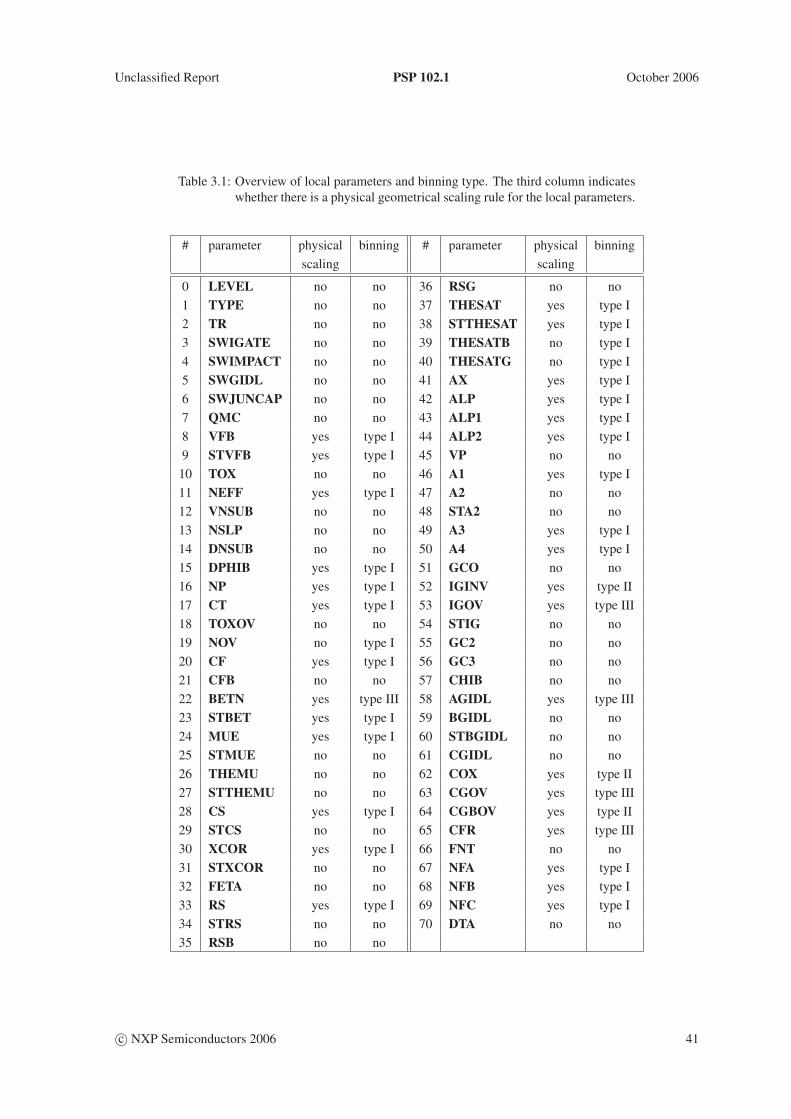
Unclassified Report PSP 102.1 October 2006
Table 3.1: Overview of local parameters and binning type. The third column indicateswhether there is a physical geometrical scaling rule for the local parameters.
# parameter physical binning # parameter physical binningscaling scaling
0 LEVEL no no 36 RSG no no1 TYPE no no 37 THESAT yes type I2 TR no no 38 STTHESAT yes type I3 SWIGATE no no 39 THESATB no type I4 SWIMPACT no no 40 THESATG no type I5 SWGIDL no no 41 AX yes type I6 SWJUNCAP no no 42 ALP yes type I7 QMC no no 43 ALP1 yes type I8 VFB yes type I 44 ALP2 yes type I9 STVFB yes type I 45 VP no no10 TOX no no 46 A1 yes type I11 NEFF yes type I 47 A2 no no12 VNSUB no no 48 STA2 no no13 NSLP no no 49 A3 yes type I14 DNSUB no no 50 A4 yes type I15 DPHIB yes type I 51 GCO no no16 NP yes type I 52 IGINV yes type II17 CT yes type I 53 IGOV yes type III18 TOXOV no no 54 STIG no no19 NOV no type I 55 GC2 no no20 CF yes type I 56 GC3 no no21 CFB no no 57 CHIB no no22 BETN yes type III 58 AGIDL yes type III23 STBET yes type I 59 BGIDL no no24 MUE yes type I 60 STBGIDL no no25 STMUE no no 61 CGIDL no no26 THEMU no no 62 COX yes type II27 STTHEMU no no 63 CGOV yes type III28 CS yes type I 64 CGBOV yes type II29 STCS no no 65 CFR yes type III30 XCOR yes type I 66 FNT no no31 STXCOR no no 67 NFA yes type I32 FETA no no 68 NFB yes type I33 RS yes type I 69 NFC yes type I34 STRS no no 70 DTA no no35 RSB no no
c© NXP Semiconductors 2006 41
October 2006 PSP 102.1 Unclassified Report
Effective length and width
LEN = 10−6 (3.85)
WEN = 10−6 (3.86)
∆LPS = LVARO ·(
1 + LVARL · LEN
L
)(3.87)
∆WOD = WVARO ·(
1 + WVARW · WEN
W
)(3.88)
LE = L−∆L = L + ∆LPS − 2 · LAP (3.89)
WE = W −∆W = W + ∆WOD − 2 ·WOT (3.90)
LE,CV = L + ∆LPS − 2 · LAP + DLQ (3.91)
WE,CV = W + ∆WOD − 2 ·WOT + DWQ (3.92)
LG,CV = L + ∆LPS + DLQ (3.93)
WG,CV = W + ∆WOD + DWQ (3.94)
Note: If the calculated LE, WE, LE,CV, WE,CV, LG,CV, or WG,CV is smaller than 1 nm (10−9 m), the valueis clipped to this lower bound of 1 nm.
Process Parameters
VFB = POVFB + PLVFB · LEN
LE+ PWVFB · WEN
WE+ PLWVFB · LEN ·WEN
LE ·WE(3.95)
STVFB = POSTVFB + PLSTVFB · LEN
LE+ PWSTVFB · WEN
WE+ PLWSTVFB · LEN ·WEN
LE ·WE(3.96)
TOX = POTOX (3.97)
NEFF = PONEFF + PLNEFF · LEN
LE+ PWNEFF · WEN
WE+ PLWNEFF · LEN ·WEN
LE ·WE(3.98)
VNSUB = POVNSUB (3.99)
NSLP = PONSLP (3.100)
DNSUB = PODNSUB (3.101)
DPHIB = PODPHIB + PLDPHIB · LEN
LE+ PWDPHIB · WEN
WE+ PLWDPHIB · LEN ·WEN
LE ·WE(3.102)
NP = PONP + PLNP · LEN
LE+ PWNP · WEN
WE+ PLWNP · LEN ·WEN
LE ·WE(3.103)
CT = POCT + PLCT · LEN
LE+ PWCT · WEN
WE+ PLWCT · LEN ·WEN
LE ·WE(3.104)
42 c© NXP Semiconductors 2006
Unclassified Report PSP 102.1 October 2006
TOXOV = POTOXOV (3.105)
NOV = PONOV + PLNOV · LEN
LE+ PWNOV · WEN
WE+ PLWNOV · LEN ·WEN
LE ·WE(3.106)
DIBL Parameters
CF = POCF + PLCF · LEN
LE+ PWCF · WEN
WE+ PLWCF · LEN ·WEN
LE ·WE(3.107)
CFB = POCFB (3.108)
Mobility Parameters
BETN = POBETN + PLBETN · LEN
LE+ PWBETN · WE
WEN+ PLWBETN · WE · LEN
WEN · LE(3.109)
STBET = POSTBET + PLSTBET · LEN
LE+ PWSTBET · WEN
WE+ PLWSTBET · LEN ·WEN
LE ·WE(3.110)
MUE = POMUE + PLMUE · LEN
LE+ PWMUE · WEN
WE+ PLWMUE · LEN ·WEN
LE ·WE(3.111)
STMUE = POSTMUE (3.112)
THEMU = POTHEMU (3.113)
STTHEMU = POSTTHEMU (3.114)
CS = POCS + PLCS · LEN
LE+ PWCS · WEN
WE+ PLWCS · LEN ·WEN
LE ·WE(3.115)
STCS = POSTCS (3.116)
XCOR = POXCOR + PLXCOR · LEN
LE+ PWXCOR · WEN
WE+ PLWXCOR · LEN ·WEN
LE ·WE(3.117)
STXCOR = POSTXCOR (3.118)
FETA = POFETA (3.119)
Series Resistance Parameters
RS = PORS + PLRS · LEN
LE+ PWRS · WEN
WE+ PLWRS · LEN ·WEN
LE ·WE(3.120)
STRS = POSTRS (3.121)
RSB = PORSB (3.122)
RSG = PORSG (3.123)
c© NXP Semiconductors 2006 43
October 2006 PSP 102.1 Unclassified Report
Velocity Saturation Parameters
THESAT = POTHESAT + PLTHESAT · LEN
LE
+ PWTHESAT · WEN
WE+ PLWTHESAT · LEN ·WEN
LE ·WE(3.124)
STTHESAT = POSTTHESAT + PLSTTHESAT · LEN
LE
+ PWSTTHESAT · WEN
WE+ PLWSTTHESAT · LEN ·WEN
LE ·WE(3.125)
THESATB = POTHESATB + PLTHESATB · LEN
LE
+ PWTHESATB · WEN
WE+ PLWTHESATB · LEN ·WEN
LE ·WE(3.126)
THESATG = POTHESATG + PLTHESATG · LEN
LE
+ PWTHESATG · WEN
WE+ PLWTHESATG · LEN ·WEN
LE ·WE(3.127)
Saturation Voltage Parameters
AX = POAX + PLAX · LEN
LE+ PWAX · WEN
WE+ PLWAX · LEN ·WEN
LE ·WE(3.128)
Channel Length Modulation (CLM) Parameters
ALP = POALP + PLALP · LEN
LE+ PWALP · WEN
WE+ PLWALP · LEN ·WEN
LE ·WE(3.129)
ALP1 = POALP1 + PLALP1 · LEN
LE+ PWALP1 · WEN
WE+ PLWALP1 · LEN ·WEN
LE ·WE(3.130)
ALP2 = POALP2 + PLALP2 · LEN
LE+ PWALP2 · WEN
WE+ PLWALP2 · LEN ·WEN
LE ·WE(3.131)
VP = POVP (3.132)
Impact Ionization (II) Parameters
A1 = POA1 + PLA1 · LEN
LE+ PWA1 · WEN
WE+ PLWA1 · LEN ·WEN
LE ·WE(3.133)
A2 = POA2 (3.134)
STA2 = POSTA2 (3.135)
44 c© NXP Semiconductors 2006
Unclassified Report PSP 102.1 October 2006
A3 = POA3 + PLA3 · LEN
LE+ PWA3 · WEN
WE+ PLWA3 · LEN ·WEN
LE ·WE(3.136)
A4 = POA4 + PLA4 · LEN
LE+ PWA4 · WEN
WE+ PLWA4 · LEN ·WEN
LE ·WE(3.137)
Gate Current Parameters
GCO = POGCO (3.138)
IGINV = POIGINV + PLIGINV · LE
LEN
+ PWIGINV · WE
WEN+ PLWIGINV · LE ·WE
LEN ·WEN(3.139)
IGOV = POIGOV + PLIGOV · LEN
LE+ PWIGOV · WE
WEN+ PLWIGOV · WE · LEN
WEN · LE(3.140)
STIG = POSTIG (3.141)
GC2 = POGC2 (3.142)
GC3 = POGC3 (3.143)
CHIB = POCHIB (3.144)
Gate-Induced Drain Leakage (GIDL) Parameters
AGIDL = POAGIDL + PLAGIDL · LEN
LE
+ PWAGIDL · WE
WEN+ PLWAGIDL · WE · LEN
WEN · LE(3.145)
BGIDL = POBGIDL (3.146)
STBGIDL = POSTBGIDL (3.147)
CGIDL = POCGIDL (3.148)
Charge Model Parameters
COX = POCOX + PLCOX · LE,CV
LEN+ PWCOX · WE,CV
WEN+ PLWCOX · LE,CV ·WE,CV
LEN ·WEN(3.149)
CGOV = POCGOV + PLCGOV · LEN
LE,CV
+ PWCGOV · WE,CV
WEN+ PLWCGOV · WE,CV · LEN
WEN · LE,CV(3.150)
c© NXP Semiconductors 2006 45
October 2006 PSP 102.1 Unclassified Report
CGBOV = POCGBOV + PLCGBOV · LG,CV
LEN
+ PWCGBOV · WG,CV
WEN+ PLWCGBOV · LG,CV ·WG,CV
LEN ·WEN(3.151)
CFR = POCFR + PLCFR · LEN
LG,CV+ PWCFR · WG,CV
WEN+ PLWCFR · WG,CV · LEN
WEN · LG,CV(3.152)
Noise Model Parameters
FNT = POFNT (3.153)
NFA = PONFA + PLNFA · LEN
LE+ PWNFA · WEN
WE+ PLWNFA · LEN ·WEN
LE ·WE(3.154)
NFB = PONFB + PLNFB · LEN
LE+ PWNFB · WEN
WE+ PLWNFB · LEN ·WEN
LE ·WE(3.155)
NFC = PONFC + PLNFC · LEN
LE+ PWNFC · WEN
WE+ PLWNFC · LEN ·WEN
LE ·WE(3.156)
46 c© NXP Semiconductors 2006
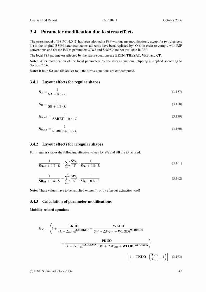
Unclassified Report PSP 102.1 October 2006
3.4 Parameter modification due to stress effects
The stress model of BSIM4.4.0 [2] has been adopted in PSP without any modifications, except for two changes:(1) in the original BSIM parameter names all zeros have been replaced by “O”s, in order to comply with PSPconventions and (2) the BSIM parameters STK2 and LODK2 are not available in PSP.
The local PSP parameters affected by the stress equations are BETN, THESAT, VFB, and CF.
Note: After modification of the local parameters by the stress equations, clipping is applied according toSection 2.5.6.
Note: If both SA and SB are set to 0, the stress-equations are not computed.
3.4.1 Layout effects for regular shapes
RA =1
SA + 0.5 · L (3.157)
RB =1
SB + 0.5 · L (3.158)
RA,ref =1
SAREF + 0.5 · L (3.159)
RB,ref =1
SBREF + 0.5 · L (3.160)
3.4.2 Layout effects for irregular shapes
For irregular shapes the following effective values for SA and SB are to be used.
1SAeff + 0.5 · L =
n∑
i=1
SWi
W· 1
SAi + 0.5 · L (3.161)
1SBeff + 0.5 · L =
n∑
i=1
SWi
W· 1
SBi + 0.5 · L (3.162)
Note: These values have to be supplied manually or by a layout extraction tool!
3.4.3 Calculation of parameter modifications
Mobility-related equations
Ku0 =
(1 +
LKUO(L + ∆LPS)LLODKUO +
WKUO(W + ∆WOD + WLOD)WLODKUO
+PKUO
(L + ∆LPS)LLODKUO · (W + ∆WOD + WLOD)WLODKUO
)
·[1 + TKUO ·
(TKD
TKR− 1
)](3.163)
c© NXP Semiconductors 2006 47
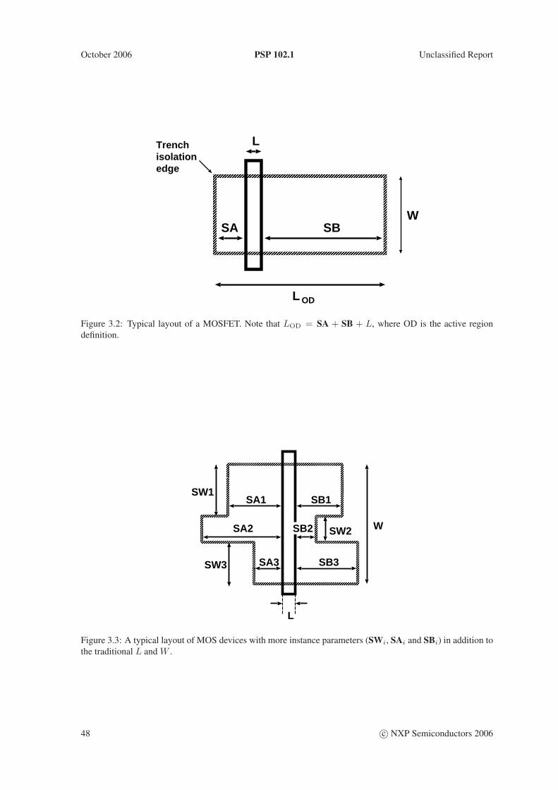
October 2006 PSP 102.1 Unclassified Report
Trench isolation edge
L
SA SBW
L OD
Figure 3.2: Typical layout of a MOSFET. Note that LOD = SA + SB + L, where OD is the active regiondefinition.
W
L
SW1SA1 SB1
SA2
SW3 SA3
SW2
SB3
SB2
Figure 3.3: A typical layout of MOS devices with more instance parameters (SWi, SAi and SBi) in addition tothe traditional L and W .
48 c© NXP Semiconductors 2006
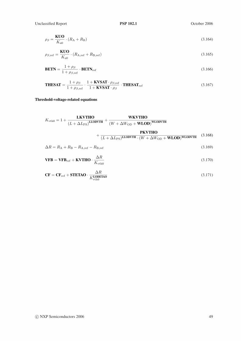
Unclassified Report PSP 102.1 October 2006
ρβ =KUOKu0
· (RA + RB) (3.164)
ρβ,ref =KUOKu0
· (RA,ref + RB,ref) (3.165)
BETN =1 + ρβ
1 + ρβ,ref· BETNref (3.166)
THESAT =1 + ρβ
1 + ρβ,ref· 1 + KVSAT · ρβ,ref
1 + KVSAT · ρβ· THESATref (3.167)
Threshold-voltage-related equations
Kvth0 = 1 +LKVTHO
(L + ∆LPS)LLODVTH +WKVTHO
(W + ∆WOD + WLOD)WLODVTH
+PKVTHO
(L + ∆LPS)LLODVTH · (W + ∆WOD + WLOD)WLODVTH (3.168)
∆R = RA + RB −RA,ref −RB,ref (3.169)
VFB = VFBref + KVTHO · ∆R
Kvth0(3.170)
CF = CFref + STETAO · ∆R
KLODETAOvth0
(3.171)
c© NXP Semiconductors 2006 49

October 2006 PSP 102.1 Unclassified Report
50 c© NXP Semiconductors 2006
Unclassified Report PSP 102.1 October 2006
Section 4
PSP Model Equations
4.1 Internal Parameters (including Temperature Scaling)
In this section, bias-independent internal parameters will be calculated, including temperature scaling. Theseparameters are computed from local parameters. Local parameters are (as usual) denoted by capital charactersin bold font, whereas the internal parameters are denoted by symbols in bold font.
Transistor temperature
TKR = T0 + TR (4.1)
TKD = T0 + TA + DTA (4.2)
∆T = TKD − TKR (4.3)
φT =kB · TKD
q(4.4)
Local process parameters
φ*T = φT ·
(1 + CT · TKR
TKD
)(4.5)
V FB = VFB + STVFB ·∆T (4.6)
Eg/q = 1.179− 9.025 · 10−5 · TKD − 3.05 · 10−7 · TKD2 (4.7)
rT =(1.045 + 4.5 · 10−4 · TKD
) · (0.523 + 1.4 · 10−3 · TKD − 1.48 · 10−6 · TKD2)
(4.8)
ni = 2.5 · 1025 · rT3/4 · (TKD/300)3/2 · exp
(− Eg/q
2 · φT
)(4.9)
φclB = MAX(DPHIB + 2 · φT · ln [NEFF/ni] , 0.05) (4.10)
Cox = εox/TOX (4.11)
γ0 =√
2 · q · εSi · NEFF/Cox (4.12)
Gcl0 = γ0/
√φT (4.13)
c© NXP Semiconductors 2006 51
October 2006 PSP 102.1 Unclassified Report
Polysilicon depletion parameter
kP =
if NP = 0
kP = 0
if NP > 0
NP1 = MAX(NP, 8 · 107/TOX2)
NP2 = MAX(NP1, 3 · 1025)
kP = 2 · φT · C2ox/(q · εSi ·NP2)
(4.14)
Quantum-mechanical correction parameters
qlim = 10 · φT (4.15)
qq =
0.4 ·QMC ·QMN · C2/3ox for NMOS
0.4 ·QMC ·QMP · C2/3ox for PMOS
(4.16)
qb0 = γ0 ·√
φclB (4.17)
φB = φclB + 0.75 · qq · q2/3
b0 (4.18)
G0 = Gcl0 ·
(1 + qq · q−1/3
b0
)(4.19)
VSB-clipping parameters
φX = 0.95 · φB (4.20)
aφ = 2.5 · 10−3 · φ2B (4.21)
bφ = 2.5 · 10−3 · φ2B (4.22)
φ?X = 0.5 ·
√bφ (4.23)
φ*X = MINA (φX − φ?
X, 0, aφ ) (4.24)
Local process parameters in gate overlap regions
γov =√
2 · q · εSi · NOV · TOXOV/εox (4.25)
Gov = γov/√
φT (4.26)
ξov = 1 + Gov/√
2 (4.27)
xmrgov = 10−5 · ξov (4.28)
52 c© NXP Semiconductors 2006
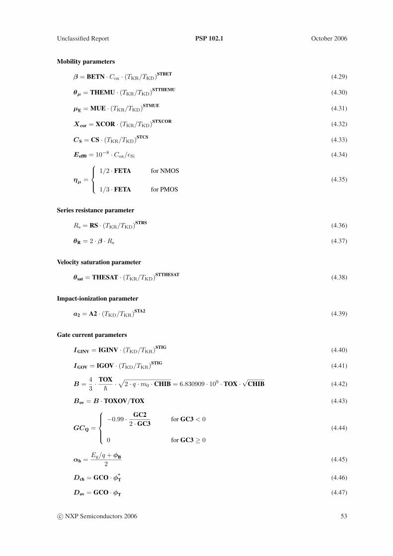
Unclassified Report PSP 102.1 October 2006
Mobility parameters
β = BETN · Cox · (TKR/TKD)STBET (4.29)
θµ = THEMU · (TKR/TKD)STTHEMU (4.30)
µE = MUE · (TKR/TKD)STMUE (4.31)
Xcor = XCOR · (TKR/TKD)STXCOR (4.32)
CS = CS · (TKR/TKD)STCS (4.33)
Eeff0 = 10−8 · Cox/εSi (4.34)
ηµ =
1/2 · FETA for NMOS
1/3 · FETA for PMOS
(4.35)
Series resistance parameter
Rs = RS · (TKR/TKD)STRS (4.36)
θR = 2 · β ·Rs (4.37)
Velocity saturation parameter
θsat = THESAT · (TKR/TKD)STTHESAT (4.38)
Impact-ionization parameter
a2 = A2 · (TKD/TKR)STA2 (4.39)
Gate current parameters
IGINV = IGINV · (TKD/TKR)STIG (4.40)
IGOV = IGOV · (TKD/TKR)STIG (4.41)
B =43· TOX~
·√
2 · q ·m0 · CHIB = 6.830909 · 109 · TOX ·√
CHIB (4.42)
Bov = B · TOXOV/TOX (4.43)
GCQ =
−0.99 · GC22 ·GC3
for GC3 < 0
0 for GC3 ≥ 0
(4.44)
αb =Eg/q + φB
2(4.45)
Dch = GCO · φ*T (4.46)
Dov = GCO · φT (4.47)
c© NXP Semiconductors 2006 53
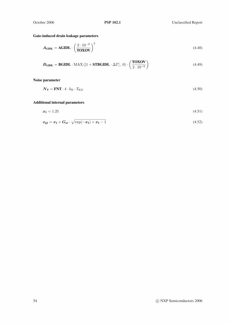
October 2006 PSP 102.1 Unclassified Report
Gate-induced drain leakage parameters
AGIDL = AGIDL ·(
2 · 10−9
TOXOV
)2
(4.48)
BGIDL = BGIDL ·MAX([1 + STBGIDL ·∆T ] , 0) ·(
TOXOV2 · 10−9
)(4.49)
Noise parameter
NT = FNT · 4 · kB · TKD (4.50)
Additional internal parameters
x1 = 1.25 (4.51)
xg1 = x1 + Gov ·√
exp(−x1) + x1 − 1 (4.52)
54 c© NXP Semiconductors 2006
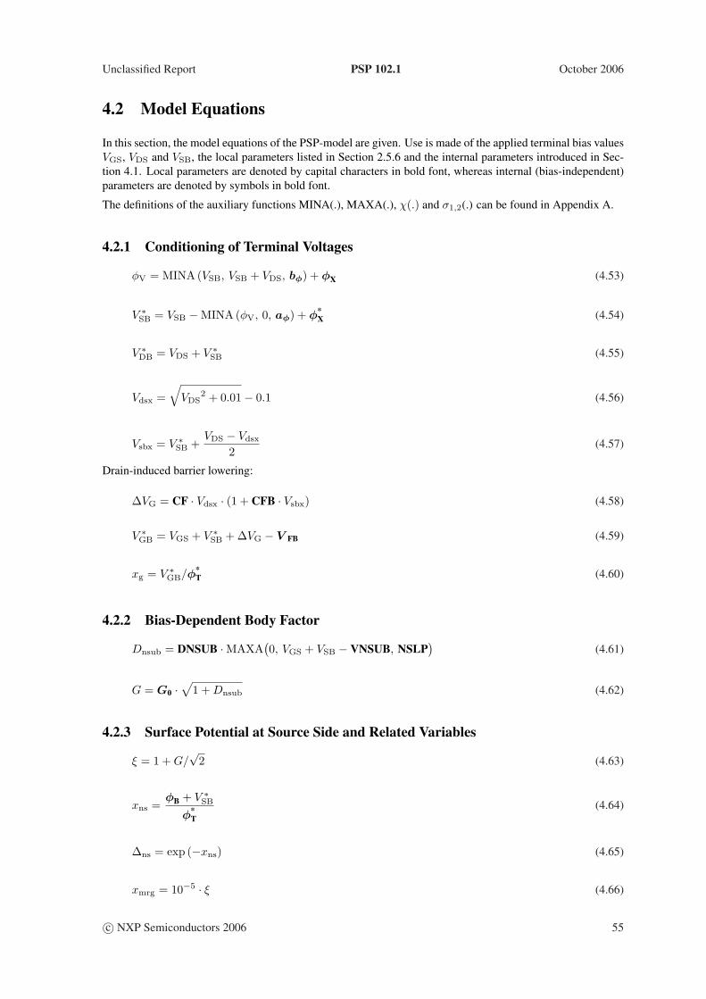
Unclassified Report PSP 102.1 October 2006
4.2 Model Equations
In this section, the model equations of the PSP-model are given. Use is made of the applied terminal bias valuesVGS, VDS and VSB, the local parameters listed in Section 2.5.6 and the internal parameters introduced in Sec-tion 4.1. Local parameters are denoted by capital characters in bold font, whereas internal (bias-independent)parameters are denoted by symbols in bold font.
The definitions of the auxiliary functions MINA(.), MAXA(.), χ(.) and σ1,2(.) can be found in Appendix A.
4.2.1 Conditioning of Terminal Voltages
φV = MINA (VSB, VSB + VDS, bφ) + φX (4.53)
V ∗SB = VSB −MINA(φV, 0, aφ) + φ*
X (4.54)
V ∗DB = VDS + V ∗
SB (4.55)
Vdsx =√
VDS2 + 0.01− 0.1 (4.56)
Vsbx = V ∗SB +
VDS − Vdsx
2(4.57)
Drain-induced barrier lowering:
∆VG = CF · Vdsx · (1 + CFB · Vsbx) (4.58)
V ∗GB = VGS + V ∗
SB + ∆VG − V FB (4.59)
xg = V ∗GB/φ*
T (4.60)
4.2.2 Bias-Dependent Body Factor
Dnsub = DNSUB ·MAXA(0, VGS + VSB − VNSUB, NSLP
)(4.61)
G = G0 ·√
1 + Dnsub (4.62)
4.2.3 Surface Potential at Source Side and Related Variables
ξ = 1 + G/√
2 (4.63)
xns =φB + V ∗
SB
φ*T
(4.64)
∆ns = exp (−xns) (4.65)
xmrg = 10−5 · ξ (4.66)
c© NXP Semiconductors 2006 55
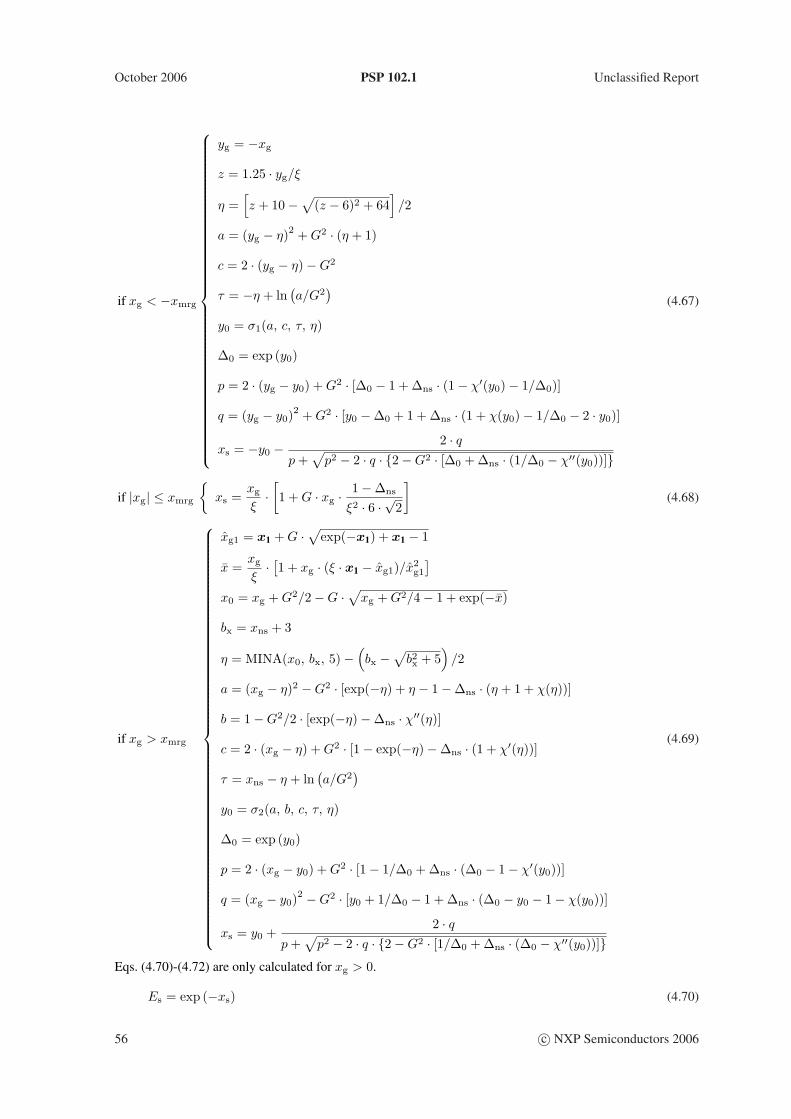
October 2006 PSP 102.1 Unclassified Report
if xg < −xmrg
yg = −xg
z = 1.25 · yg/ξ
η =[z + 10−
√(z − 6)2 + 64
]/2
a = (yg − η)2 + G2 · (η + 1)
c = 2 · (yg − η)−G2
τ = −η + ln(a/G2
)
y0 = σ1(a, c, τ, η)
∆0 = exp (y0)
p = 2 · (yg − y0) + G2 · [∆0 − 1 + ∆ns · (1− χ′(y0)− 1/∆0)]
q = (yg − y0)2 + G2 · [y0 −∆0 + 1 + ∆ns · (1 + χ(y0)− 1/∆0 − 2 · y0)]
xs = −y0 − 2 · qp +
√p2 − 2 · q · 2−G2 · [∆0 + ∆ns · (1/∆0 − χ′′(y0))]
(4.67)
if |xg| ≤ xmrg
xs =
xg
ξ·[1 + G · xg · 1−∆ns
ξ2 · 6 · √2
](4.68)
if xg > xmrg
xg1 = x1 + G ·√
exp(−x1) + x1 − 1
x =xg
ξ· [1 + xg · (ξ · x1 − xg1)/x2
g1
]
x0 = xg + G2/2−G ·√xg + G2/4− 1 + exp(−x)
bx = xns + 3
η = MINA(x0, bx, 5)−(bx −
√b2x + 5
)/2
a = (xg − η)2 −G2 · [exp(−η) + η − 1−∆ns · (η + 1 + χ(η))]
b = 1−G2/2 · [exp(−η)−∆ns · χ′′(η)]
c = 2 · (xg − η) + G2 · [1− exp(−η)−∆ns · (1 + χ′(η))]
τ = xns − η + ln(a/G2
)
y0 = σ2(a, b, c, τ, η)
∆0 = exp (y0)
p = 2 · (xg − y0) + G2 · [1− 1/∆0 + ∆ns · (∆0 − 1− χ′(y0))]
q = (xg − y0)2 −G2 · [y0 + 1/∆0 − 1 + ∆ns · (∆0 − y0 − 1− χ(y0))]
xs = y0 +2 · q
p +√
p2 − 2 · q · 2−G2 · [1/∆0 + ∆ns · (∆0 − χ′′(y0))]
(4.69)
Eqs. (4.70)-(4.72) are only calculated for xg > 0.
Es = exp (−xs) (4.70)
56 c© NXP Semiconductors 2006
Unclassified Report PSP 102.1 October 2006
Ds = [1/Es − xs − 1− χ(xs)] ·∆ns (4.71)
Ps = xs − 1 + Es (4.72)
xgs =
xg − xs for xg ≤ 0
G · √Ds + Ps for xg > 0(4.73)
ψss = φ*T · xs (4.74)
4.2.4 Drain Saturation Voltage
Eqs. (4.75)-(4.95) are only calculated for xg > 0.
qis =G2 · φ*
T ·Ds
xgs + G · √Ps
(4.75)
αs = 1 +G · (1− Es)
2 · √Ps
(4.76)
qbs = φ*T ·G ·
√Ps (4.77)
ρb =
1 + RSB · Vsbx for RSB ≥ 0
11− RSB · Vsbx
for RSB < 0(4.78)
ρg,s =
11 + RSG · qis
for RSG ≥ 0
1− RSG · qis for RSG < 0
(4.79)
ρs = θR · ρb · ρg,s · qis (4.80)
µx =1 + Xcor · Vsbx
1 + 0.2 ·Xcor · Vsbx(4.81)
Eeff,s = Eeff0 ·(qbs + ηµ · qis
)(4.82)
Gmob,s =1 + (µE · Eeff,s)
θµ + CS ·(
qbs
qis + qbs
)2
+ ρs
µx(4.83)
ξtb =
1 + THESATB · Vsbx for THESATB ≥ 0
11− THESATB · Vsbx
for THESATB < 0(4.84)
wsat,s =100 · qis · ξtb
100 + qis · ξtb(4.85)
c© NXP Semiconductors 2006 57
October 2006 PSP 102.1 Unclassified Report
θ∗sat,s =
θsat
Gmob,s· (1 + THESATG · wsat,s) for THESATG ≥ 0
θsat
Gmob,s· 11− THESATG · wsat,s
for THESATG < 0
(4.86)
φ∞ = qis/αs + φ*T (4.87)
ysat =
θ∗sat,s · φ∞/√
2 for NMOS
θ∗sat,s · φ∞/√
2√1 + θ∗sat,s · φ∞/
√2
for PMOS(4.88)
za =2
1 +√
1 + 4 · ysat(4.89)
φ0 = φ∞ · za ·[1 + 0.86 · za · ysat · 1− z2
a · ysat
1 + 4 · z3a · y2
sat
](4.90)
asat = xgs + G2/2 (4.91)
φ2 =φ*
T · 0.98 ·G2 ·Ds
asat +√
a2sat − 0.98 ·G2 ·Ds
(4.92)
φsat =2 · φ0 · φ2
φ0 + φ2 +√
(φ0 + φ2)2 − 3.96 · φ0 · φ2
(4.93)
Vdsat = φsat − φ*T · ln
1 +
φsat ·(φsat − 2 · asat · φ*
T
)
G2 ·Ds · φ*T2
(4.94)
Vdse =VDS[
1 + (VDS/Vdsat)AX
]1/AX (4.95)
4.2.5 Surface Potential at Drain Side and Related Variables
Eqs. (4.96)-(4.105) are only calculated for xg > 0.
xnd =φB + V ∗
SB + Vdse
φ*T
(4.96)
kds = exp(−Vdse/φ*
T
)(4.97)
∆nd = ∆ns · kds (4.98)
if xg ≤ xmrg
xd =
xg
ξ·[1 + G · xg · 1−∆nd
ξ2 · 6 · √2
](4.99)
58 c© NXP Semiconductors 2006
Unclassified Report PSP 102.1 October 2006
if xg > xmrg
bx = xnd + 3.0
η = MINA(x0, bx, 5)−(bx −
√b2x + 5
)/2
a = (xg − η)2 −G2 · [exp(−η) + η − 1−∆nd · (η + 1 + χ(η))]
b = 1−G2/2 · [exp(−η)−∆nd · χ′′(η)]
c = 2 · (xg − η) + G2 · [1− exp(−η)−∆nd · (1 + χ′(η))]
τ = xnd − η + ln(a/G2
)
y0 = σ2(a, b, c, τ, η)
∆0 = exp (y0)
p = 2 · (xg − y0) + G2 · [1− 1/∆0 + ∆nd · (∆0 − 1− χ′(y0))]
q = (xg − y0)2 −G2 · [y0 + 1/∆0 − 1 + ∆nd · (∆0 − y0 − 1− χ(y0))]
xd = y0 +2 · q
p +√
p2 − 2 · q · 2−G2 · [1/∆0 + ∆nd · (∆0 − χ′′(y0))]
(4.100)
xds = xd − xs (4.101)
if xds < 10−10
p = 2 · xgs + G2 · [1− Es + ∆nd · (1/Es − 1− χ′(xs))]
q = G2 · (1− kds) ·Ds
ξ = 1−G2/2 · [Es + ∆nd (1/Es − χ′′(xs))]
xds =2 · q
p +√
p2 − 4 · ξ · qxd = xs + xds
(4.102)
Ed = exp (−xd) (4.103)
Dd = (1/Ed − xd − 1− χ(xd)) ·∆nd (4.104)
∆ψ = φ*T · xds (4.105)
ψsd = φ*T · xd (4.106)
4.2.6 Mid-Point Surface Potential and Related Variables
if xg > 0
xm = (xs + xd) /2
Em =√
Es · Ed
D = (Ds + Dd) /2
Dm = D + x2ds/8 · (Em − 2/G2
)
Pm = xm − 1 + Em
xgm = G · √Dm + Pm
(4.107)
c© NXP Semiconductors 2006 59
October 2006 PSP 102.1 Unclassified Report
if xg ≤ 0
xm = xs
xgm = xg − xs
(4.108)
4.2.7 Polysilicon Depletion
Eqs. (4.109)-(4.123) are only calculated for kP > 0 and xg > 0 (otherwise ηp = 1):
x(0)m = xm, x
(0)ds = xds, D(0)
m = Dm, E(0)m = Em, (4.109)
d0 = 1− E(0)m + 2 · xgm/G2 (4.110)
ηp = 1/√
1 + kP · xgm (4.111)
xpm = kP ·[ηp · xgm
1 + ηp
]2
· D(0)m
D(0)m + Pm
(4.112)
p = 2 · (xgm − xpm) + G2 ·(1− E(0)
m + D(0)m
)(4.113)
q = xpm · (xpm − 2 · xgm) (4.114)
ξp = 1−G2/2 ·(E(0)
m + D(0)m
)(4.115)
up =p · q
p2 − ξp · q (4.116)
xm = x(0)m + up (4.117)
Em = E(0)m · exp (−up) (4.118)
Dm = D(0)m · exp (up) (4.119)
Pm = xm − 1 + Em (4.120)
xgm = G ·√
Dm + Pm (4.121)
xds = x(0)ds ·
exp (up) · [D + d0
]
1− Em + 2 · xgm · ηp/G2 + exp (up) · D (4.122)
∆ψ = φ*T · xds (4.123)
60 c© NXP Semiconductors 2006
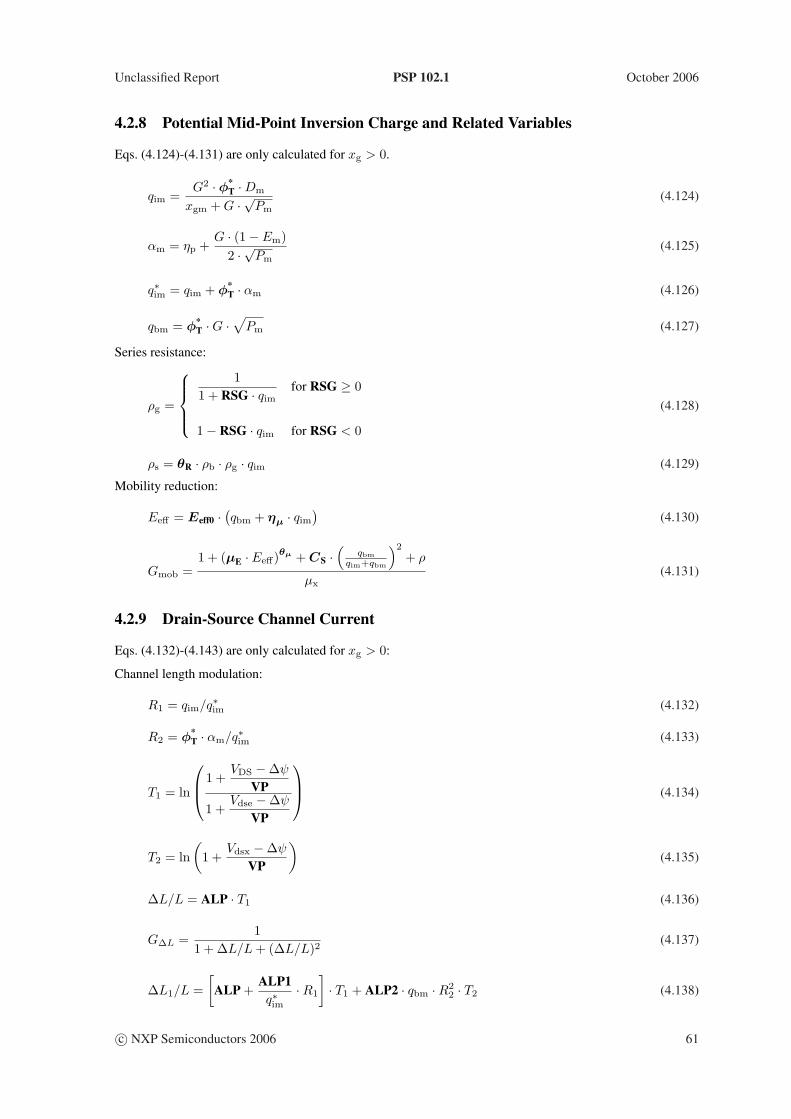
Unclassified Report PSP 102.1 October 2006
4.2.8 Potential Mid-Point Inversion Charge and Related Variables
Eqs. (4.124)-(4.131) are only calculated for xg > 0.
qim =G2 · φ*
T ·Dm
xgm + G · √Pm
(4.124)
αm = ηp +G · (1− Em)
2 · √Pm
(4.125)
q∗im = qim + φ*T · αm (4.126)
qbm = φ*T ·G ·
√Pm (4.127)
Series resistance:
ρg =
11 + RSG · qim
for RSG ≥ 0
1− RSG · qim for RSG < 0
(4.128)
ρs = θR · ρb · ρg · qim (4.129)
Mobility reduction:
Eeff = Eeff0 ·(qbm + ηµ · qim
)(4.130)
Gmob =1 + (µE · Eeff)θµ + CS ·
(qbm
qim+qbm
)2
+ ρ
µx(4.131)
4.2.9 Drain-Source Channel Current
Eqs. (4.132)-(4.143) are only calculated for xg > 0:
Channel length modulation:
R1 = qim/q∗im (4.132)
R2 = φ*T · αm/q∗im (4.133)
T1 = ln
1 +VDS −∆ψ
VP
1 +Vdse −∆ψ
VP
(4.134)
T2 = ln(
1 +Vdsx −∆ψ
VP
)(4.135)
∆L/L = ALP · T1 (4.136)
G∆L =1
1 + ∆L/L + (∆L/L)2(4.137)
∆L1/L =[
ALP +ALP1q∗im
·R1
]· T1 + ALP2 · qbm ·R2
2 · T2 (4.138)
c© NXP Semiconductors 2006 61
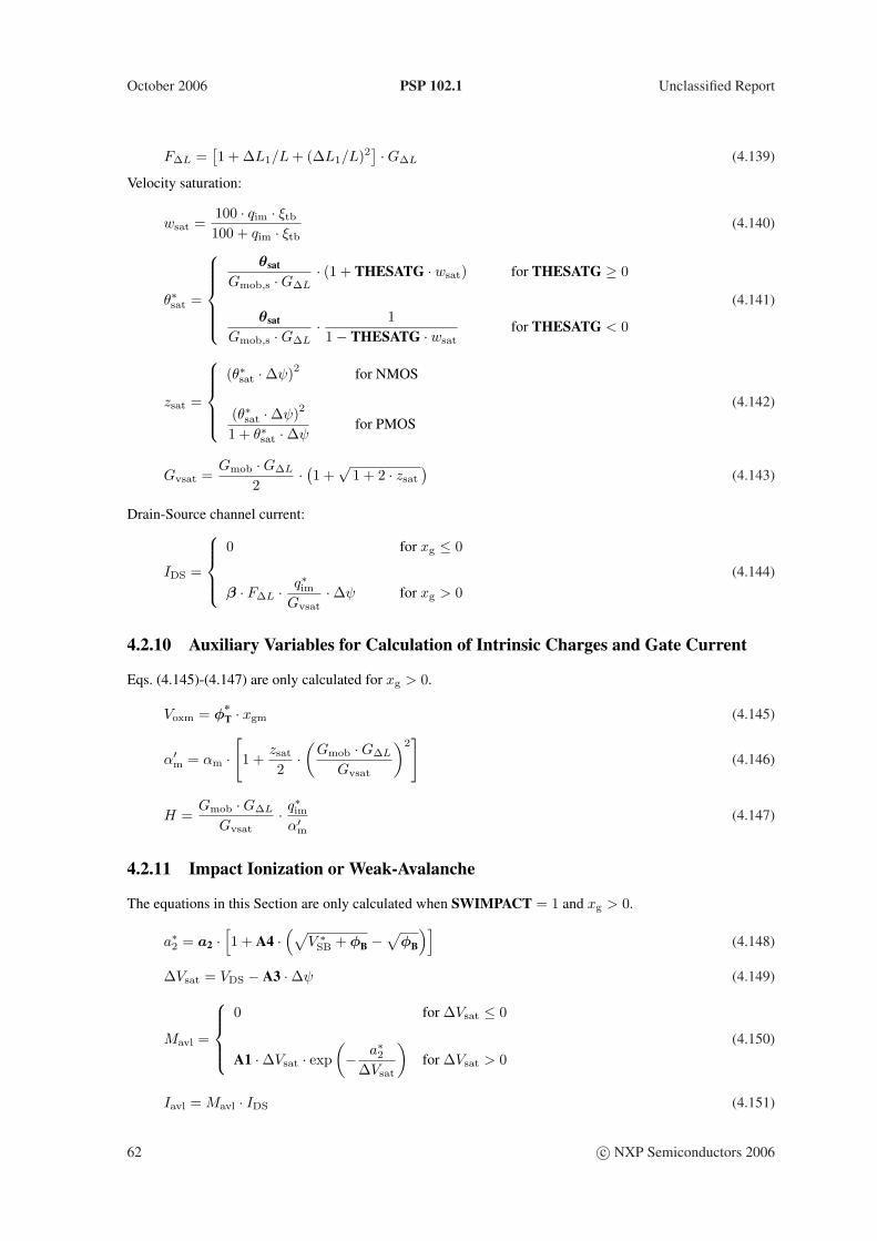
October 2006 PSP 102.1 Unclassified Report
F∆L =[1 + ∆L1/L + (∆L1/L)2
] ·G∆L (4.139)
Velocity saturation:
wsat =100 · qim · ξtb
100 + qim · ξtb(4.140)
θ∗sat =
θsat
Gmob,s ·G∆L· (1 + THESATG · wsat) for THESATG ≥ 0
θsat
Gmob,s ·G∆L· 11− THESATG · wsat
for THESATG < 0
(4.141)
zsat =
(θ∗sat ·∆ψ)2 for NMOS
(θ∗sat ·∆ψ)2
1 + θ∗sat ·∆ψfor PMOS
(4.142)
Gvsat =Gmob ·G∆L
2· (1 +
√1 + 2 · zsat
)(4.143)
Drain-Source channel current:
IDS =
0 for xg ≤ 0
β · F∆L · q∗imGvsat
·∆ψ for xg > 0(4.144)
4.2.10 Auxiliary Variables for Calculation of Intrinsic Charges and Gate Current
Eqs. (4.145)-(4.147) are only calculated for xg > 0.
Voxm = φ*T · xgm (4.145)
α′m = αm ·[1 +
zsat
2·(
Gmob ·G∆L
Gvsat
)2]
(4.146)
H =Gmob ·G∆L
Gvsat· q∗imα′m
(4.147)
4.2.11 Impact Ionization or Weak-Avalanche
The equations in this Section are only calculated when SWIMPACT = 1 and xg > 0.
a∗2 = a2 ·[1 + A4 ·
(√V ∗
SB + φB −√
φB
)](4.148)
∆Vsat = VDS − A3 ·∆ψ (4.149)
Mavl =
0 for ∆Vsat ≤ 0
A1 ·∆Vsat · exp(− a∗2
∆Vsat
)for ∆Vsat > 0
(4.150)
Iavl = Mavl · IDS (4.151)
62 c© NXP Semiconductors 2006
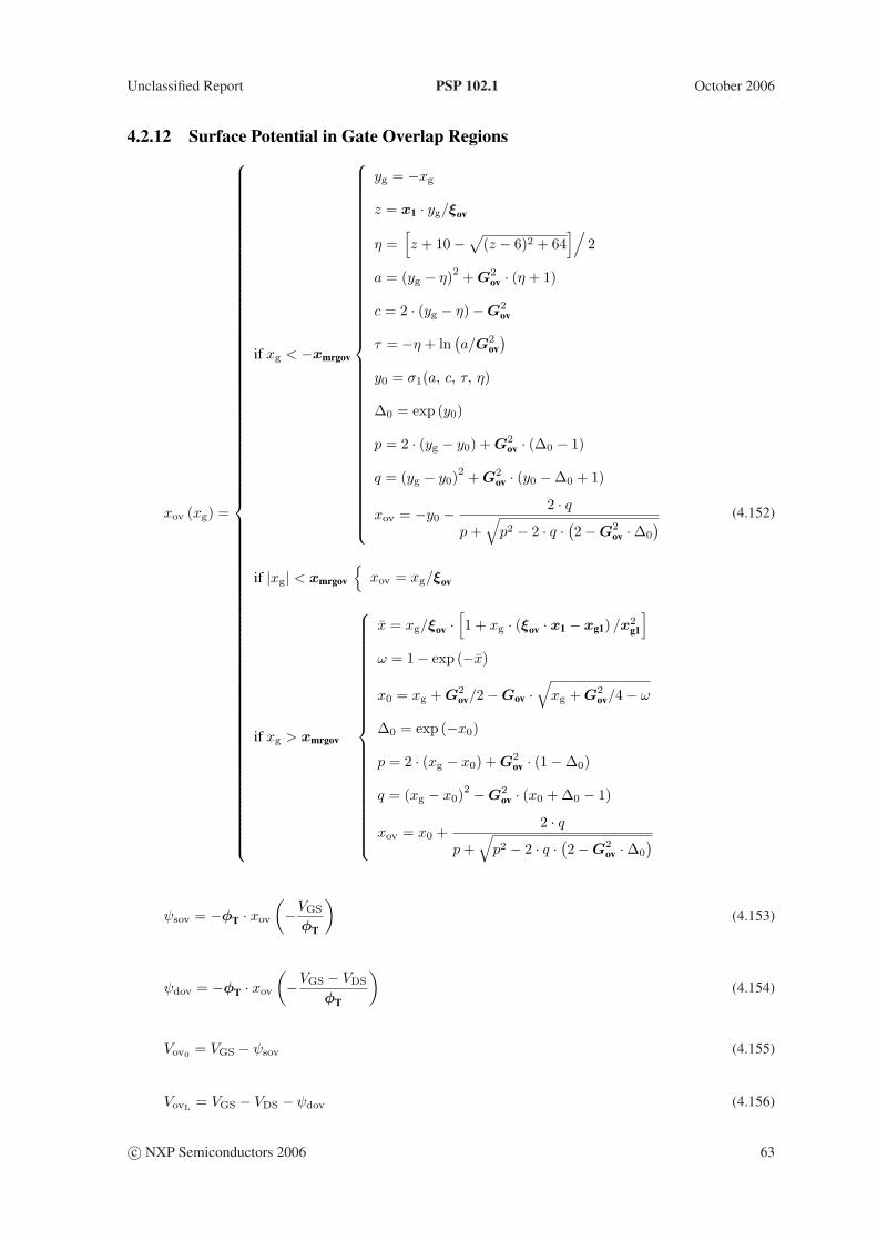
Unclassified Report PSP 102.1 October 2006
4.2.12 Surface Potential in Gate Overlap Regions
xov (xg) =
if xg < −xmrgov
yg = −xg
z = x1 · yg/ξov
η =[z + 10−
√(z − 6)2 + 64
]/2
a = (yg − η)2 + G2ov · (η + 1)
c = 2 · (yg − η)−G2ov
τ = −η + ln(a/G2
ov)
y0 = σ1(a, c, τ, η)
∆0 = exp (y0)
p = 2 · (yg − y0) + G2ov · (∆0 − 1)
q = (yg − y0)2 + G2
ov · (y0 −∆0 + 1)
xov = −y0 − 2 · qp +
√p2 − 2 · q · (2−G2
ov ·∆0
)
if |xg| < xmrgov
xov = xg/ξov
if xg > xmrgov
x = xg/ξov ·[1 + xg · (ξov · x1 − xg1) /x2
g1
]
ω = 1− exp (−x)
x0 = xg + G2ov/2−Gov ·
√xg + G2
ov/4− ω
∆0 = exp (−x0)
p = 2 · (xg − x0) + G2ov · (1−∆0)
q = (xg − x0)2 −G2
ov · (x0 + ∆0 − 1)
xov = x0 +2 · q
p +√
p2 − 2 · q · (2−G2ov ·∆0
)
(4.152)
ψsov = −φT · xov
(−VGS
φT
)(4.153)
ψdov = −φT · xov
(−VGS − VDS
φT
)(4.154)
Vov0 = VGS − ψsov (4.155)
VovL = VGS − VDS − ψdov (4.156)
c© NXP Semiconductors 2006 63
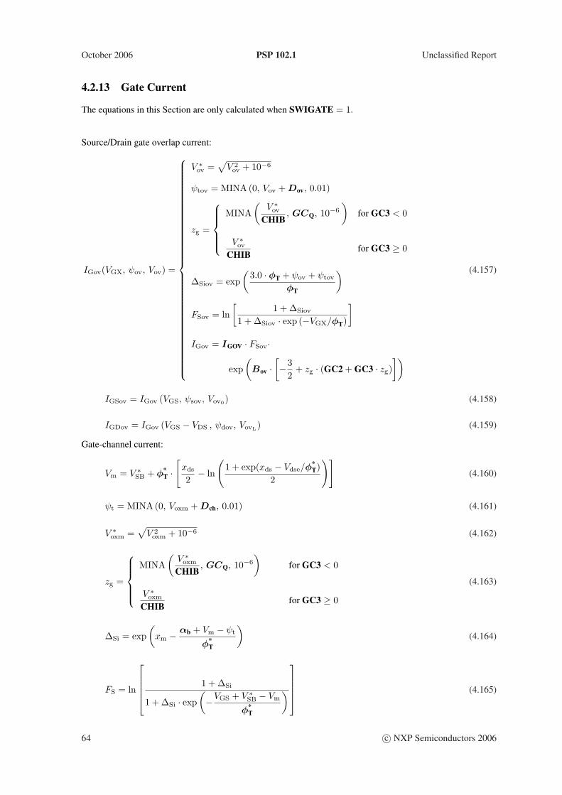
October 2006 PSP 102.1 Unclassified Report
4.2.13 Gate Current
The equations in this Section are only calculated when SWIGATE = 1.
Source/Drain gate overlap current:
IGov(VGX, ψov, Vov) =
V ∗ov =
√V 2
ov + 10−6
ψtov = MINA (0, Vov + Dov, 0.01)
zg =
MINA(
V ∗ov
CHIB, GCQ, 10−6
)for GC3 < 0
V ∗ov
CHIBfor GC3 ≥ 0
∆Siov = exp(
3.0 · φT + ψov + ψtov
φT
)
FSov = ln[
1 + ∆Siov
1 + ∆Siov · exp (−VGX/φT)
]
IGov = IGOV · FSov·
exp(
Bov ·[−3
2+ zg · (GC2 + GC3 · zg)
])
(4.157)
IGSov = IGov (VGS, ψsov, Vov0) (4.158)
IGDov = IGov (VGS − VDS , ψdov, VovL) (4.159)
Gate-channel current:
Vm = V ∗SB + φ*
T ·[
xds
2− ln
(1 + exp(xds − Vdse/φ*
T)2
)](4.160)
ψt = MINA (0, Voxm + Dch, 0.01) (4.161)
V ∗oxm =
√V 2
oxm + 10−6 (4.162)
zg =
MINA(
V ∗oxm
CHIB, GCQ, 10−6
)for GC3 < 0
V ∗oxm
CHIBfor GC3 ≥ 0
(4.163)
∆Si = exp(
xm − αb + Vm − ψt
φ*T
)(4.164)
FS = ln
1 + ∆Si
1 + ∆Si · exp(−VGS + V ∗
SB − Vm
φ*T
)
(4.165)
64 c© NXP Semiconductors 2006
Unclassified Report PSP 102.1 October 2006
IGCO = IGINV · FS · exp (B · [−3/2 + zg · (GC2 + GC3 · zg)]) (4.166)
if xg > 0
u0 = CHIB/ [B · (GC2 + 2 ·GC3 · zg)]
x = ∆ψ/ (2 · u0)
b = u0/H
Bg = b · (1− b) /2
Ag = 1/2− 3 ·Bg
pgc = (1− b) · sinh(x)x
+ b · cosh(x)
pgd =pgc
2−Bg · sinh(x)−Ag · sinh(x)
x·[coth(x)− 1
x
]
(4.167)
if xg ≤ 0
pgc = 1
pgd = 1/2(4.168)
Sg =12·1 +
xg√x2
g + 10−6
(4.169)
IGC = IGCO · pgc · Sg (4.170)
IGCD = IGCO · pgd · Sg (4.171)
IGCS = IGC − IGCD (4.172)
IGB = IGCO · pgc · (1− Sg) (4.173)
4.2.14 Gate-Induced Drain/Source Leakage Current
The equations in this section are only calculated when SWGIDL = 1.
Igixl(Vov, V ) =
Vtov =√
V 2ov + CGIDL2 · V 2 + 10−6
t = V · Vtov · Vov
Igixl =
−AGIDL · t · exp(−BGIDL
Vtov
)for Vov < 0
0 for Vov ≥ 0
(4.174)
Igisl = Igixl(Vov0 , VSB) (4.175)
Igidl = Igixl(VovL , VDS + VSB) (4.176)
c© NXP Semiconductors 2006 65
October 2006 PSP 102.1 Unclassified Report
4.2.15 Total Terminal Currents
ID = IDS + Iavl − IGDov − IGCD + Igidl (4.177)
IS = −IDS − IGSov − IGCS + Igisl (4.178)
IG = IGC + IGB + IGDov + IGSov (4.179)
IB = −Iavl − IGB − Igidl − Igisl (4.180)
66 c© NXP Semiconductors 2006
Unclassified Report PSP 102.1 October 2006
4.2.16 Quantum-Mechanical Corrections
qeff =
Voxm for xg ≤ 0
qbm + ηµ · qim for xg > 0(4.181)
CqmOX =
COX for qq = 0
COX1 + qq/(qeff
2 + qlim2)1/6
for qq > 0(4.182)
4.2.17 Intrinsic Charge Model
if xg > 0
Fj = ∆ψ/ (2 ·H)
q∆L = (1−G∆L) · (qim − αm ·∆ψ/2)
q∗∆L = q∆L · (1 + G∆L)
Q(i)G = Cqm
OX ·[Voxm +
ηp ·∆ψ
2·(
G∆L
3· Fj + G∆L − 1
)]
Q(i)I = −Cqm
OX ·[G∆L ·
(qim +
αm ·∆ψ
6· Fj
)+ q∆L
]
Q(i)D = −Cqm
OX
2·[G2
∆L ·(
qim +αm ·∆ψ
6·[
F 2j
5+ Fj − 1
])+ q∗∆L
]
(4.183)
if xg ≤ 0
Q(i)G = Cqm
OX · Voxm
Q(i)I = 0
Q(i)D = 0
(4.184)
Q(i)S = Q
(i)I −Q
(i)D (4.185)
Q(i)B = −Q
(i)I −Q
(i)G (4.186)
4.2.18 Extrinsic Charge Model
The charges of the source and drain overlap regions:
Qsov = CGOV · (VGS − ψsov) (4.187)
Qdov = CGOV · (VGS − VDS − ψdov) (4.188)
The charge of the bulk overlap region
Qbov = CGBOV · (VGS − VSB) (4.189)
Outer fringe charge:
Qofs = CFR · VGS (4.190)
Qofd = CFR · (VGS − VDS) (4.191)
c© NXP Semiconductors 2006 67
October 2006 PSP 102.1 Unclassified Report
4.2.19 Total Terminal Charges
QG = Q(i)G + Qsov + Qdov + Qofs + Qofd + Qbov (4.192)
QS = Q(i)S −Qsov −Qofs (4.193)
QD = Q(i)D −Qdov −Qofd (4.194)
QB = Q(i)B −Qbov (4.195)
68 c© NXP Semiconductors 2006
Unclassified Report PSP 102.1 October 2006
4.2.20 Noise Model
Eqs. (4.196)-(4.212) are only calculated for xg > 0. In these equations fop represents the operation frequencyof the transistor and j =
√−1.
N∗ =Cox
q· αm · φT (4.196)
N∗m =
Cox
q· q∗im (4.197)
∆N =Cox
q· αm ·∆ψ (4.198)
Sfl =q · φ2
T · β · IDS
fop · Cox ·Gvsat ·N∗ ·[(NFA− NFB ·N∗ + NFC ·N∗ 2) · ln
(N∗
m + ∆N/2N∗
m −∆N/2
)
+(
NFB + NFC · [N∗m − 2 ·N∗]
)·∆N
](4.199)
H0 =q∗imαm
(4.200)
t1 =qim
q∗im(4.201)
t2 =(
∆ψ
12 ·H0
)2
(4.202)
R =H0
H− 1 (4.203)
lc = 1− 12 · t2 ·R (4.204)
gideal =β · q∗imGvsat
· F∆L (4.205)
CGeff =(
Gvsat
Gmob ·G∆L
)2
· CqmOX · ηp (4.206)
mid =gideal
l2c· [t1 + 12 · t2 − 24 · (1 + t1) · t2 ·R] (4.207)
Sid = NT ·mid (4.208)
mig =1
l2c · gideal·[
t112− t2 ·
(t1 +
15− 12 · t2
)− 8
5· t2 · (t1 + 1− 12 · t2) ·R
](4.209)
Sig = NT · (2 · π · fop · CGeff)2 ·mig
1 + (2 · π · fop · CGeff ·mig)2(4.210)
c© NXP Semiconductors 2006 69
October 2006 PSP 102.1 Unclassified Report
migid =√
t2l2c
·[1− 12 · t2 −
(t1 +
965· t2 − 12 · t1 · t2
)·R
](4.211)
Sigid = NT · 2 · π · j · fop · CGeff ·migid
1 + 2 · π · j · fop · CGeff ·mig(4.212)
Gate current shot noise:
Sigs = 2 · q · (IGCS + IGSov) (4.213)
Sigd = 2 · q · (IGCD + IGDov) (4.214)
Avalanche current shot noise:
Savl = 2 · q · (1 + Mavl) · Iavl (4.215)
70 c© NXP Semiconductors 2006
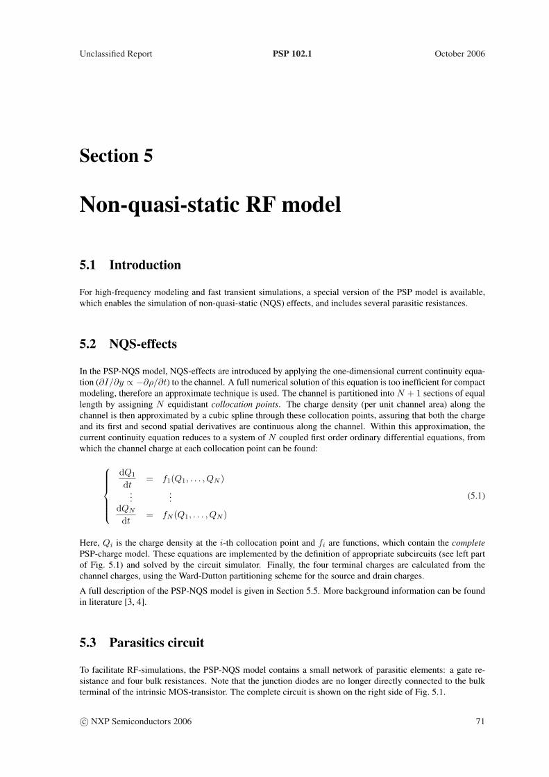
Unclassified Report PSP 102.1 October 2006
Section 5
Non-quasi-static RF model
5.1 Introduction
For high-frequency modeling and fast transient simulations, a special version of the PSP model is available,which enables the simulation of non-quasi-static (NQS) effects, and includes several parasitic resistances.
5.2 NQS-effects
In the PSP-NQS model, NQS-effects are introduced by applying the one-dimensional current continuity equa-tion (∂I/∂y ∝ −∂ρ/∂t) to the channel. A full numerical solution of this equation is too inefficient for compactmodeling, therefore an approximate technique is used. The channel is partitioned into N + 1 sections of equallength by assigning N equidistant collocation points. The charge density (per unit channel area) along thechannel is then approximated by a cubic spline through these collocation points, assuring that both the chargeand its first and second spatial derivatives are continuous along the channel. Within this approximation, thecurrent continuity equation reduces to a system of N coupled first order ordinary differential equations, fromwhich the channel charge at each collocation point can be found:
dQ1
dt= f1(Q1, . . . , QN )
......
dQN
dt= fN (Q1, . . . , QN )
(5.1)
Here, Qi is the charge density at the i-th collocation point and fi are functions, which contain the completePSP-charge model. These equations are implemented by the definition of appropriate subcircuits (see left partof Fig. 5.1) and solved by the circuit simulator. Finally, the four terminal charges are calculated from thechannel charges, using the Ward-Dutton partitioning scheme for the source and drain charges.
A full description of the PSP-NQS model is given in Section 5.5. More background information can be foundin literature [3, 4].
5.3 Parasitics circuit
To facilitate RF-simulations, the PSP-NQS model contains a small network of parasitic elements: a gate re-sistance and four bulk resistances. Note that the junction diodes are no longer directly connected to the bulkterminal of the intrinsic MOS-transistor. The complete circuit is shown on the right side of Fig. 5.1.
c© NXP Semiconductors 2006 71
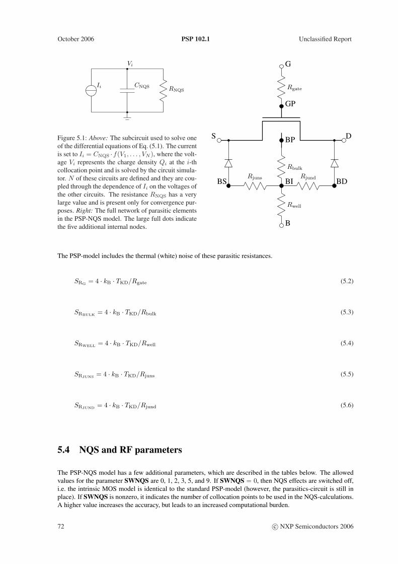
October 2006 PSP 102.1 Unclassified Report
RNQS
Vi
Ii CNQS
Figure 5.1: Above: The subcircuit used to solve oneof the differential equations of Eq. (5.1). The currentis set to Ii = CNQS ·f(V1, . . . , VN ), where the volt-age Vi represents the charge density Qi at the i-thcollocation point and is solved by the circuit simula-tor. N of these circuits are defined and they are cou-pled through the dependence of Ii on the voltages ofthe other circuits. The resistance RNQS has a verylarge value and is present only for convergence pur-poses. Right: The full network of parasitic elementsin the PSP-NQS model. The large full dots indicatethe five additional internal nodes.
G
DS
BD
Rgate
Rwell
RjundRjuns
Rbulk
BP
GP
BS
B
BI
The PSP-model includes the thermal (white) noise of these parasitic resistances.
SRG = 4 · kB · TKD/Rgate (5.2)
SRBULK = 4 · kB · TKD/Rbulk (5.3)
SRWELL = 4 · kB · TKD/Rwell (5.4)
SRJUNS = 4 · kB · TKD/Rjuns (5.5)
SRJUND = 4 · kB · TKD/Rjund (5.6)
5.4 NQS and RF parameters
The PSP-NQS model has a few additional parameters, which are described in the tables below. The allowedvalues for the parameter SWNQS are 0, 1, 2, 3, 5, and 9. If SWNQS = 0, then NQS effects are switched off,i.e. the intrinsic MOS model is identical to the standard PSP-model (however, the parasitics-circuit is still inplace). If SWNQS is nonzero, it indicates the number of collocation points to be used in the NQS-calculations.A higher value increases the accuracy, but leads to an increased computational burden.
72 c© NXP Semiconductors 2006
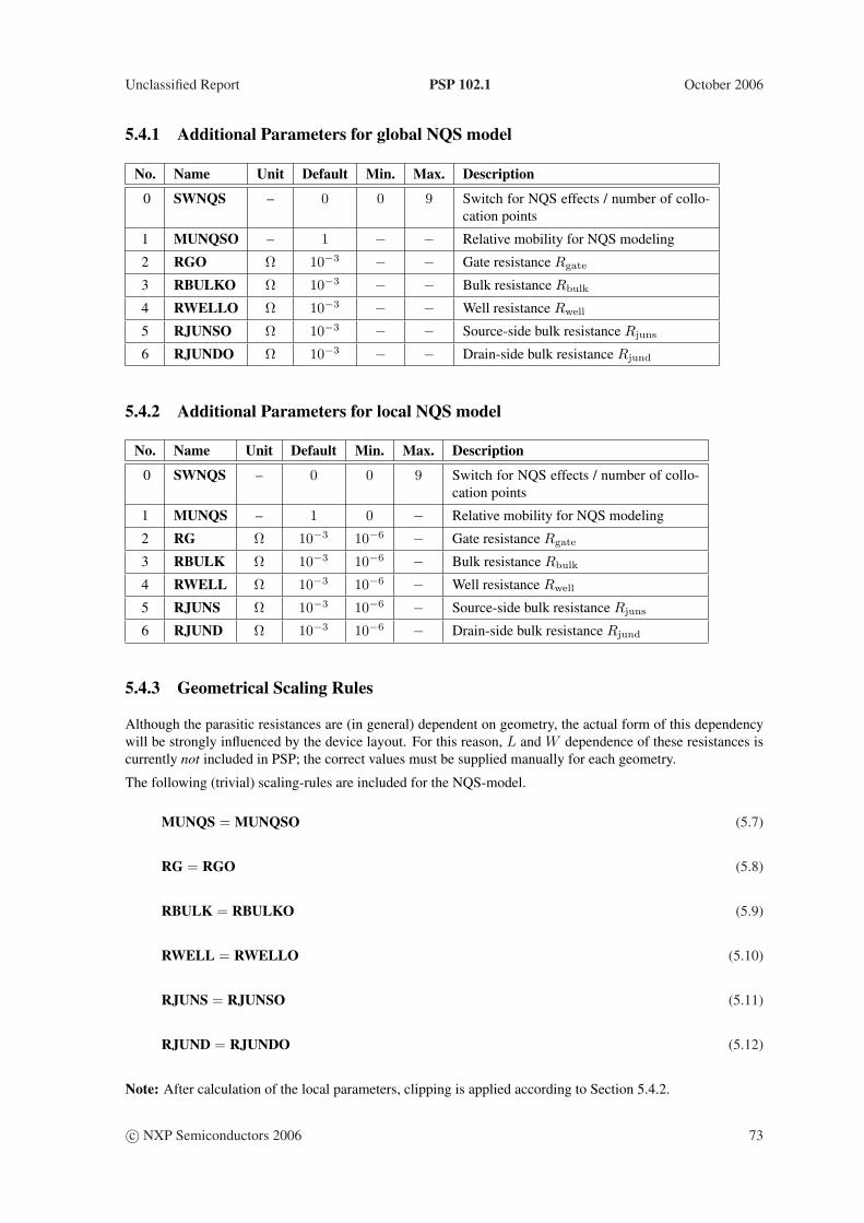
Unclassified Report PSP 102.1 October 2006
5.4.1 Additional Parameters for global NQS model
No. Name Unit Default Min. Max. Description
0 SWNQS – 0 0 9 Switch for NQS effects / number of collo-cation points
1 MUNQSO – 1 − − Relative mobility for NQS modeling
2 RGO Ω 10−3 − − Gate resistance Rgate
3 RBULKO Ω 10−3 − − Bulk resistance Rbulk
4 RWELLO Ω 10−3 − − Well resistance Rwell
5 RJUNSO Ω 10−3 − − Source-side bulk resistance Rjuns
6 RJUNDO Ω 10−3 − − Drain-side bulk resistance Rjund
5.4.2 Additional Parameters for local NQS model
No. Name Unit Default Min. Max. Description
0 SWNQS – 0 0 9 Switch for NQS effects / number of collo-cation points
1 MUNQS – 1 0 − Relative mobility for NQS modeling
2 RG Ω 10−3 10−6 − Gate resistance Rgate
3 RBULK Ω 10−3 10−6 − Bulk resistance Rbulk
4 RWELL Ω 10−3 10−6 − Well resistance Rwell
5 RJUNS Ω 10−3 10−6 − Source-side bulk resistance Rjuns
6 RJUND Ω 10−3 10−6 − Drain-side bulk resistance Rjund
5.4.3 Geometrical Scaling Rules
Although the parasitic resistances are (in general) dependent on geometry, the actual form of this dependencywill be strongly influenced by the device layout. For this reason, L and W dependence of these resistances iscurrently not included in PSP; the correct values must be supplied manually for each geometry.
The following (trivial) scaling-rules are included for the NQS-model.
MUNQS = MUNQSO (5.7)
RG = RGO (5.8)
RBULK = RBULKO (5.9)
RWELL = RWELLO (5.10)
RJUNS = RJUNSO (5.11)
RJUND = RJUNDO (5.12)
Note: After calculation of the local parameters, clipping is applied according to Section 5.4.2.
c© NXP Semiconductors 2006 73
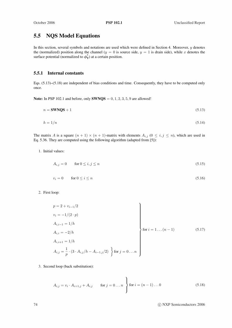
October 2006 PSP 102.1 Unclassified Report
5.5 NQS Model Equations
In this section, several symbols and notations are used which were defined in Section 4. Moreover, y denotesthe (normalized) position along the channel (y = 0 is source side, y = 1 is drain side), while x denotes thesurface potential (normalized to φ*
T) at a certain position.
5.5.1 Internal constants
Eqs. (5.13)–(5.18) are independent of bias conditions and time. Consequently, they have to be computed onlyonce.
Note: In PSP 102.1 and before, only SWNQS = 0, 1, 2, 3, 5, 9 are allowed!
n = SWNQS + 1 (5.13)
h = 1/n (5.14)
The matrix A is a square (n + 1) × (n + 1)-matrix with elements Ai,j (0 ≤ i, j ≤ n), which are used inEq. 5.36. They are computed using the following algorithm (adapted from [5]):
1. Initial values:
Ai,j = 0 for 0 ≤ i, j ≤ n (5.15)
vi = 0 for 0 ≤ i ≤ n (5.16)
2. First loop:
p = 2 + vi−1/2
vi = −1/(2 · p)
Ai,i−1 = 1/h
Ai,i = −2/h
Ai,i+1 = 1/h
Ai,j =1p· (3 ·Ai,j/h−Ai−1,j/2)
for j = 0 . . . n
for i = 1 . . . (n− 1) (5.17)
3. Second loop (back substitution):
Ai,j = vi ·Ai+1,j + Ai,j for j = 0 . . . n
for i = (n− 1) . . . 0 (5.18)
74 c© NXP Semiconductors 2006
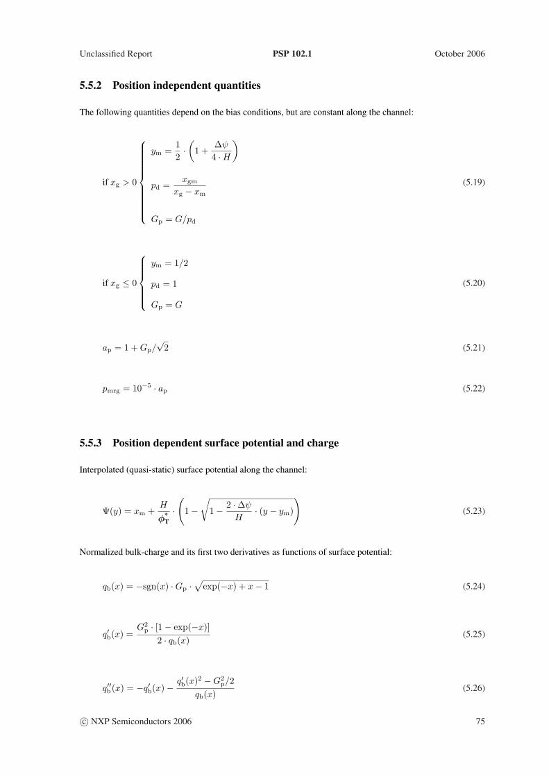
Unclassified Report PSP 102.1 October 2006
5.5.2 Position independent quantities
The following quantities depend on the bias conditions, but are constant along the channel:
if xg > 0
ym =12·(
1 +∆ψ
4 ·H)
pd =xgm
xg − xm
Gp = G/pd
(5.19)
if xg ≤ 0
ym = 1/2
pd = 1
Gp = G
(5.20)
ap = 1 + Gp/√
2 (5.21)
pmrg = 10−5 · ap (5.22)
5.5.3 Position dependent surface potential and charge
Interpolated (quasi-static) surface potential along the channel:
Ψ(y) = xm +H
φ*T·(
1−√
1− 2 ·∆ψ
H· (y − ym)
)(5.23)
Normalized bulk-charge and its first two derivatives as functions of surface potential:
qb(x) = −sgn(x) ·Gp ·√
exp(−x) + x− 1 (5.24)
q′b(x) =G2
p · [1− exp(−x)]2 · qb(x)
(5.25)
q′′b(x) = −q′b(x)− q′b(x)2 −G2p/2
qb(x)(5.26)
c© NXP Semiconductors 2006 75
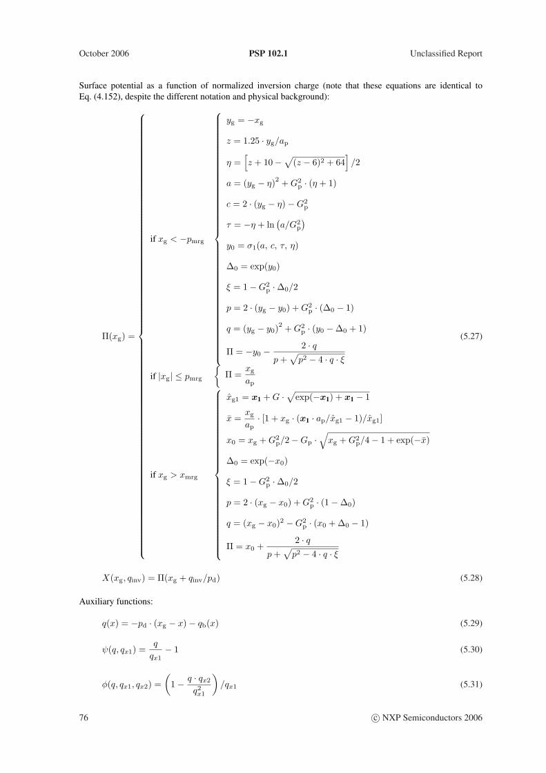
October 2006 PSP 102.1 Unclassified Report
Surface potential as a function of normalized inversion charge (note that these equations are identical toEq. (4.152), despite the different notation and physical background):
Π(xg) =
if xg < −pmrg
yg = −xg
z = 1.25 · yg/ap
η =[z + 10−
√(z − 6)2 + 64
]/2
a = (yg − η)2 + G2p · (η + 1)
c = 2 · (yg − η)−G2p
τ = −η + ln(a/G2
p
)
y0 = σ1(a, c, τ, η)
∆0 = exp(y0)
ξ = 1−G2p ·∆0/2
p = 2 · (yg − y0) + G2p · (∆0 − 1)
q = (yg − y0)2 + G2
p · (y0 −∆0 + 1)
Π = −y0 − 2 · qp +
√p2 − 4 · q · ξ
if |xg| ≤ pmrg
Π =
xg
ap
if xg > xmrg
xg1 = x1 + G ·√
exp(−x1) + x1 − 1
x =xg
ap· [1 + xg · (x1 · ap/xg1 − 1)/xg1]
x0 = xg + G2p/2−Gp ·
√xg + G2
p/4− 1 + exp(−x)
∆0 = exp(−x0)
ξ = 1−G2p ·∆0/2
p = 2 · (xg − x0) + G2p · (1−∆0)
q = (xg − x0)2 −G2p · (x0 + ∆0 − 1)
Π = x0 +2 · q
p +√
p2 − 4 · q · ξ
(5.27)
X(xg, qinv) = Π(xg + qinv/pd) (5.28)
Auxiliary functions:
q(x) = −pd · (xg − x)− qb(x) (5.29)
ψ(q, qx1) =q
qx1− 1 (5.30)
φ(q, qx1, qx2) =(
1− q · qx2
q2x1
)/qx1 (5.31)
76 c© NXP Semiconductors 2006
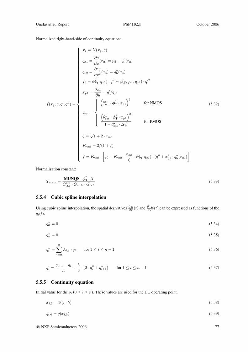
Unclassified Report PSP 102.1 October 2006
Normalized right-hand-side of continuity equation:
f(xg, q, q′, q′′) =
xz = X(xg, q)
qx1 =∂q
∂x(xz) = pd − q′b(xz)
qx2 =∂2q
∂x2(xz) = q′′b(xz)
f0 = ψ(q, qx1) · q′′ + φ(q, qx1, qx2) · q′2
xy1 =∂xz
∂y= q′/qx1
zsat =
(θ∗sat · φ*
T · xy1
)2
for NMOS
(θ∗sat · φ*
T · xy1
)2
1 + θ∗sat ·∆ψfor PMOS
ζ =√
1 + 2 · zsat
Fvsat = 2/(1 + ζ)
f = Fvsat ·[f0 − Fvsat · zsat
ζ· ψ(q, qx1) · (q′′ + x2
y1 · q′′b(xz))]
(5.32)
Normalization constant:
Tnorm =MUNQS · φ*
T · βCqm
OX ·Gmob ·G∆L(5.33)
5.5.4 Cubic spline interpolation
Using cubic spline interpolation, the spatial derivatives ∂qi
∂y (t) and ∂2qi
∂y2 (t) can be expressed as functions of theqi(t).
q′′0 = 0 (5.34)
q′′n = 0 (5.35)
q′′i =n∑
j=0
Ai,j · qi for 1 ≤ i ≤ n− 1 (5.36)
q′i =qi+1 − qi
h− h
6· (2 · q′′i + q′′i+1) for 1 ≤ i ≤ n− 1 (5.37)
5.5.5 Continuity equation
Initial value for the qi (0 ≤ i ≤ n). These values are used for the DC operating point.
xi,0 = Ψ(i · h) (5.38)
qi,0 = q(xi,0) (5.39)
c© NXP Semiconductors 2006 77
October 2006 PSP 102.1 Unclassified Report
Note: x0,0 = xs and xn,0 = xd. Moreover, these values coincide with those in the quasi-static part of PSP.
The core of the NQS-model is the solution of q(y, t) from the charge continuity equation along the channel.By approximating the y-dependence by a cubic spline through a number of collocation points, the problem isreduced to solving the qi(t) from the following set of coupled differential equations.
∂qi
∂t(t) + Tnorm · f
(xg, qi(t),
∂qi
∂y(t),
∂2qi
∂y2(t)
)= 0
qi(0) = qi,0
for 1 ≤ i ≤ n− 1 (5.40)
Note that the boundary points q0(t) = q(xs) = qis and qn(t) = q(xd) = qid remain fixed to their quasi-staticvalues; they are not solved from the equation above.
The set of differential equations defined above is solved by the circuit simulator via the subcircuits shown inthe left part of Fig. 5.1.
5.5.6 Non-quasi-static terminal charges
Once the qi are known, the NQS terminal charges can be computed:
S0 =n−1∑
i=1
qi (5.41)
S2 =n−1∑
i=1
q′′i (5.42)
qNQSI =
∫ 1
0
q(y) dy = h · S0 +h
2· (u0 + un)− h3
12· S2 (5.43)
U0 =n−1∑
i=1
i · qi (5.44)
U2 =n−1∑
i=1
i · q′′i (5.45)
qNQSD =
∫ 1
0
y · q(y) dy = h2 · U0 +h2
6· [q0 + (3n− 1)un]− h4
12· U2 (5.46)
qNQSS = qNQS
I − qNQSD (5.47)
Currently, only SWNQS = 0, 1, 2, 3, 5, 9 are allowed. For odd values of SWNQS the gate charge is integratedalong the channel using “Simpson’s rule”. If SWNQS = 2, “Simpson’s 3/8-rule” is used.
• If SWNQS is odd (that is, n is even):
qNQSG = pd ·
[xg − h
3·(
X(xg, q0) + 4 ·n/2∑
i=1
X(xg, q2i−1)+
2 ·n/2−1∑
i=1
X(xg, q2i) + X(xg, qn))]
(5.48)
78 c© NXP Semiconductors 2006
Unclassified Report PSP 102.1 October 2006
• If SWNQS = 2 (that is, n = 3):
qNQSG = pd ·
[xg − 3 · h
8· (X(xg, q0) + 3 ·X(xg, q1) + 3 ·X(xg, q2) + X(xg, q3))
](5.49)
Convert back to conventional units:
QNQSS = Cqm
OX · φ*T · qNQS
S (5.50)
QNQSD = Cqm
OX · φ*T · qNQS
D (5.51)
QNQSG = Cqm
OX · φ*T · qNQS
G (5.52)
QNQSB = −(QNQS
S + QNQSD + QNQS
G ) (5.53)
c© NXP Semiconductors 2006 79
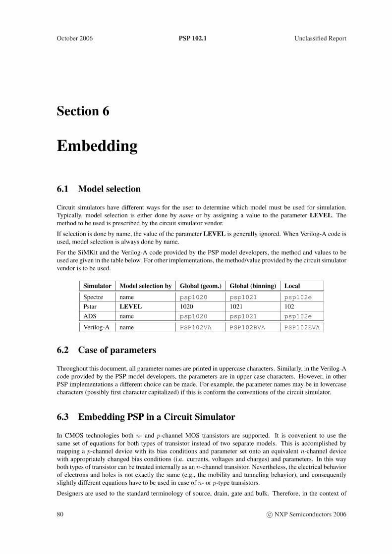
October 2006 PSP 102.1 Unclassified Report
Section 6
Embedding
6.1 Model selection
Circuit simulators have different ways for the user to determine which model must be used for simulation.Typically, model selection is either done by name or by assigning a value to the parameter LEVEL. Themethod to be used is prescribed by the circuit simulator vendor.
If selection is done by name, the value of the parameter LEVEL is generally ignored. When Verilog-A code isused, model selection is always done by name.
For the SiMKit and the Verilog-A code provided by the PSP model developers, the method and values to beused are given in the table below. For other implementations, the method/value provided by the circuit simulatorvendor is to be used.
Simulator Model selection by Global (geom.) Global (binning) Local
Spectre name psp1020 psp1021 psp102e
Pstar LEVEL 1020 1021 102ADS name psp1020 psp1021 psp102e
Verilog-A name PSP102VA PSP102BVA PSP102EVA
6.2 Case of parameters
Throughout this document, all parameter names are printed in uppercase characters. Similarly, in the Verilog-Acode provided by the PSP model developers, the parameters are in upper case characters. However, in otherPSP implementations a different choice can be made. For example, the parameter names may be in lowercasecharacters (possibly first character capitalized) if this is conform the conventions of the circuit simulator.
6.3 Embedding PSP in a Circuit Simulator
In CMOS technologies both n- and p-channel MOS transistors are supported. It is convenient to use thesame set of equations for both types of transistor instead of two separate models. This is accomplished bymapping a p-channel device with its bias conditions and parameter set onto an equivalent n-channel devicewith appropriately changed bias conditions (i.e. currents, voltages and charges) and parameters. In this wayboth types of transistor can be treated internally as an n-channel transistor. Nevertheless, the electrical behaviorof electrons and holes is not exactly the same (e.g., the mobility and tunneling behavior), and consequentlyslightly different equations have to be used in case of n- or p-type transistors.
Designers are used to the standard terminology of source, drain, gate and bulk. Therefore, in the context of
80 c© NXP Semiconductors 2006
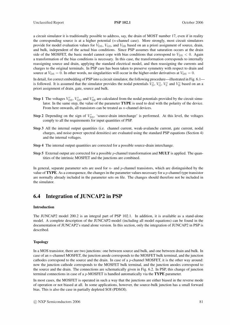
Unclassified Report PSP 102.1 October 2006
a circuit simulator it is traditionally possible to address, say, the drain of MOST number 17, even if in realitythe corresponding source is at a higher potential (n-channel case). More strongly, most circuit simulatorsprovide for model evaluation values for VDS, VGS, and VSB based on an a priori assignment of source, drain,and bulk, independent of the actual bias conditions. Since PSP assumes that saturation occurs at the drainside of the MOSFET, the basic model cannot cope with bias conditions that correspond to VDS < 0. Againa transformation of the bias conditions is necessary. In this case, the transformation corresponds to internallyreassigning source and drain, applying the standard electrical model, and then reassigning the currents andcharges to the original terminals. In PSP care has been taken to preserve symmetry with respect to drain andsource at VDS = 0. In other words, no singularities will occur in the higher-order derivatives at VDS = 0.
In detail, for correct embedding of PSP into a circuit simulator, the following procedure—illustrated in Fig. 6.1—is followed. It is assumed that the simulator provides the nodal potentials V e
D, V eG, V e
S and V eB based on an a
priori assignment of drain, gate, source and bulk.
Step 1 The voltages V ′DS, V ′
GS, and V ′SB are calculated from the nodal potentials provided by the circuit simu-
lator. In the same step, the value of the parameter TYPE is used to deal with the polarity of the device.From here onwards, all transistors can be treated as n-channel devices.
Step 2 Depending on the sign of V ′DS, ‘source-drain interchange’ is performed. At this level, the voltages
comply to all the requirements for input quantities of PSP.
Step 3 All the internal output quantities (i.e. channel current, weak-avalanche current, gate current, nodalcharges, and noise-power spectral densities) are evaluated using the standard PSP equations (Section 4)and the internal voltages.
Step 4 The internal output quantities are corrected for a possible source-drain interchange.
Step 5 External output are corrected for a possible p-channel transformation and MULT is applied. The quan-tities of the intrinsic MOSFET and the junctions are combined.
In general, separate parameter sets are used for n- and p-channel transistors, which are distinguished by thevalue of TYPE. As a consequence, the changes in the parameter values necessary for a p-channel type transistorare normally already included in the parameter sets on file. The changes should therefore not be included inthe simulator.
6.4 Integration of JUNCAP2 in PSP
Introduction
The JUNCAP2 model 200.2 is an integral part of PSP 102.1. In addition, it is available as a stand-alonemodel. A complete description of the JUNCAP2-model (including all model equations) can be found in thedocumentation of JUNCAP2’s stand alone version. In this section, only the integration of JUNCAP2 in PSP isdescribed.
Topology
In a MOS transistor, there are two junctions: one between source and bulk, and one between drain and bulk. Incase of an n-channel MOSFET, the junction anode corresponds to the MOSFET bulk terminal, and the junctioncathodes correspond to the source and the drain. In case of a p-channel MOSFET, it is the other way around:now the junction cathode corresponds to the MOSFET bulk terminal, and the junction anodes correspond tothe source and the drain. The connections are schematically given in Fig. 6.2. In PSP, this change of junctionterminal connections in case of a p-MOSFET is handled automatically via the TYPE parameter.
In most cases, the MOSFET is operated in such a way that the junctions are either biased in the reverse modeof operation or not biased at all. In some applications, however, the source-bulk junction has a small forwardbias. This is also the case in partially depleted SOI (PDSOI).
c© NXP Semiconductors 2006 81
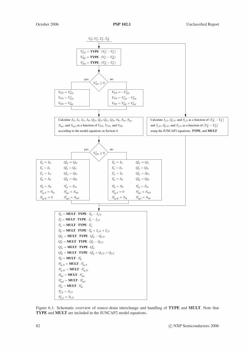
October 2006 PSP 102.1 Unclassified Report
V eD, V e
G, V eS , V e
B
V ′GS = TYPE · (V e
G − V eS )
V ′SB = TYPE · (V e
S − V eB)
V ′DS = TYPE · (V e
D − V eS )
yes noV ′
DS ≥ 0
VDS = V ′DS
VGS = V ′GS
VSB = V ′SB
VDS = −V ′DS
VGS = V ′GS − V ′
DS
VSB = V ′SB + V ′
DS
according to the model equations in Section 4.
Sigs, and Sigd as a function of VDS, VGS, and VSB
Calculate ID, IS, IG, IB, QD, QS, QG, QB, Sfl, Sid, Sig,
V ′DS ≥ 0
yes no
I ′D = ID
I ′S = IS
I ′B = IB
Q′D = QD
Q′S = QS
Q′G = QG
Q′B = QB
I ′D = IS
I ′S = ID
I ′B = IB
Q′D = QS
Q′S = QD
Q′G = QG
Q′B = QB
S′fl = Sfl
S′ig,S = Sig
S′id = Sid
S′igs = Sigs
S′ig,D = 0 S′igd = Sigd
S′fl = Sfl S′id = Sid
S′igs = Sigd
S′ig,D = Sig S′igd = Sigs
I ′G = IG I ′G = IG
QeD = MULT · TYPE ·Q′
D −Qj,D
QeB = MULT · TYPE ·Q′
B + Qj,D + Qj,S
QeG = MULT · TYPE ·Q′G
QeS = MULT · TYPE ·Q′
S −Qj,S
IeB = MULT · TYPE · I ′B + Ij,D + Ij,S
IeG = MULT · TYPE · I ′G
IeS = MULT · TYPE · I ′S − Ij,S
Sefl = MULT · S′fl
Seig,S = MULT · S′ig,S
Seig,D = MULT · S′ig,D
Seigs = MULT · S′igs
Seigd = MULT · S′igd
Seid = MULT · S′id
Sej,S = Sj,S
Sej,D = Sj,D
IeD = MULT · TYPE · I ′D − Ij,D
using the JUNCAP2 equations, TYPE, and MULT
and Ij,D, Qj,D, and Sj,D as a function of (V eB − V e
D)
Calculate Ij,S, Qj,S, and Sj,S as a function of (V eB − V e
S )
S′ig,S = 0
Figure 6.1: Schematic overview of source-drain interchange and handling of TYPE and MULT. Note thatTYPE and MULT are included in the JUNCAP2 model equations.
82 c© NXP Semiconductors 2006
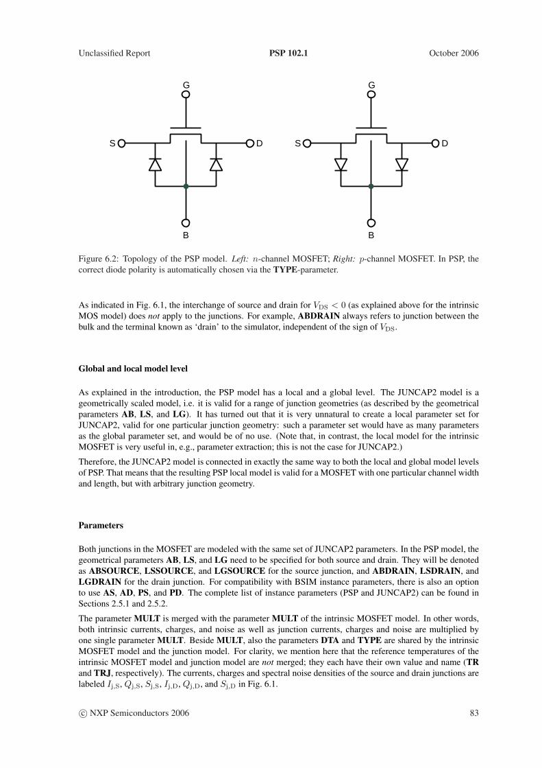
Unclassified Report PSP 102.1 October 2006
G
S D
B
G
S D
B
Figure 6.2: Topology of the PSP model. Left: n-channel MOSFET; Right: p-channel MOSFET. In PSP, thecorrect diode polarity is automatically chosen via the TYPE-parameter.
As indicated in Fig. 6.1, the interchange of source and drain for VDS < 0 (as explained above for the intrinsicMOS model) does not apply to the junctions. For example, ABDRAIN always refers to junction between thebulk and the terminal known as ‘drain’ to the simulator, independent of the sign of VDS.
Global and local model level
As explained in the introduction, the PSP model has a local and a global level. The JUNCAP2 model is ageometrically scaled model, i.e. it is valid for a range of junction geometries (as described by the geometricalparameters AB, LS, and LG). It has turned out that it is very unnatural to create a local parameter set forJUNCAP2, valid for one particular junction geometry: such a parameter set would have as many parametersas the global parameter set, and would be of no use. (Note that, in contrast, the local model for the intrinsicMOSFET is very useful in, e.g., parameter extraction; this is not the case for JUNCAP2.)
Therefore, the JUNCAP2 model is connected in exactly the same way to both the local and global model levelsof PSP. That means that the resulting PSP local model is valid for a MOSFET with one particular channel widthand length, but with arbitrary junction geometry.
Parameters
Both junctions in the MOSFET are modeled with the same set of JUNCAP2 parameters. In the PSP model, thegeometrical parameters AB, LS, and LG need to be specified for both source and drain. They will be denotedas ABSOURCE, LSSOURCE, and LGSOURCE for the source junction, and ABDRAIN, LSDRAIN, andLGDRAIN for the drain junction. For compatibility with BSIM instance parameters, there is also an optionto use AS, AD, PS, and PD. The complete list of instance parameters (PSP and JUNCAP2) can be found inSections 2.5.1 and 2.5.2.
The parameter MULT is merged with the parameter MULT of the intrinsic MOSFET model. In other words,both intrinsic currents, charges, and noise as well as junction currents, charges and noise are multiplied byone single parameter MULT. Beside MULT, also the parameters DTA and TYPE are shared by the intrinsicMOSFET model and the junction model. For clarity, we mention here that the reference temperatures of theintrinsic MOSFET model and junction model are not merged; they each have their own value and name (TRand TRJ, respectively). The currents, charges and spectral noise densities of the source and drain junctions arelabeled Ij,S, Qj,S, Sj,S, Ij,D, Qj,D, and Sj,D in Fig. 6.1.
c© NXP Semiconductors 2006 83
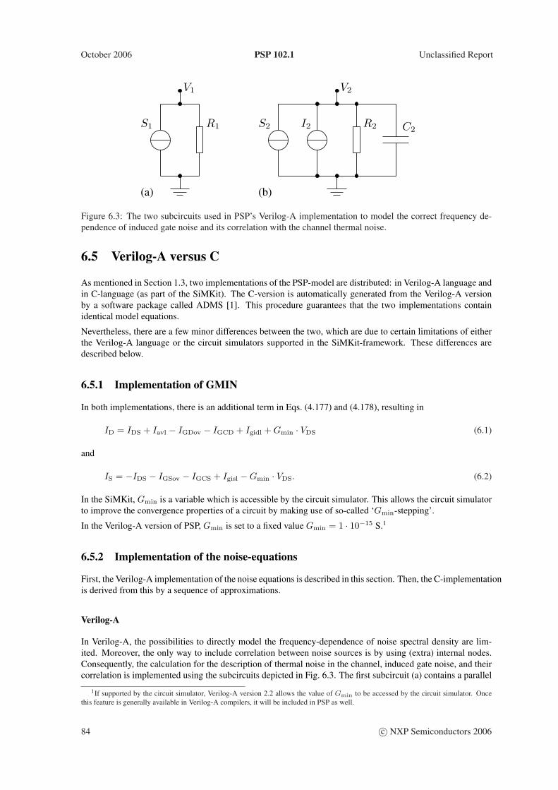
October 2006 PSP 102.1 Unclassified Report
R1 R2
(b)(a)
V1 V2
C2S2 I2S1
Figure 6.3: The two subcircuits used in PSP’s Verilog-A implementation to model the correct frequency de-pendence of induced gate noise and its correlation with the channel thermal noise.
6.5 Verilog-A versus C
As mentioned in Section 1.3, two implementations of the PSP-model are distributed: in Verilog-A language andin C-language (as part of the SiMKit). The C-version is automatically generated from the Verilog-A versionby a software package called ADMS [1]. This procedure guarantees that the two implementations containidentical model equations.
Nevertheless, there are a few minor differences between the two, which are due to certain limitations of eitherthe Verilog-A language or the circuit simulators supported in the SiMKit-framework. These differences aredescribed below.
6.5.1 Implementation of GMIN
In both implementations, there is an additional term in Eqs. (4.177) and (4.178), resulting in
ID = IDS + Iavl − IGDov − IGCD + Igidl + Gmin · VDS (6.1)
and
IS = −IDS − IGSov − IGCS + Igisl −Gmin · VDS. (6.2)
In the SiMKit, Gmin is a variable which is accessible by the circuit simulator. This allows the circuit simulatorto improve the convergence properties of a circuit by making use of so-called ‘Gmin-stepping’.
In the Verilog-A version of PSP, Gmin is set to a fixed value Gmin = 1 · 10−15 S.1
6.5.2 Implementation of the noise-equations
First, the Verilog-A implementation of the noise equations is described in this section. Then, the C-implementationis derived from this by a sequence of approximations.
Verilog-A
In Verilog-A, the possibilities to directly model the frequency-dependence of noise spectral density are lim-ited. Moreover, the only way to include correlation between noise sources is by using (extra) internal nodes.Consequently, the calculation for the description of thermal noise in the channel, induced gate noise, and theircorrelation is implemented using the subcircuits depicted in Fig. 6.3. The first subcircuit (a) contains a parallel
1If supported by the circuit simulator, Verilog-A version 2.2 allows the value of Gmin to be accessed by the circuit simulator. Oncethis feature is generally available in Verilog-A compilers, it will be included in PSP as well.
84 c© NXP Semiconductors 2006
Unclassified Report PSP 102.1 October 2006
connection of a white noise current source S1 and a resistor R1. The voltage over the elements is denotedby V1. The second subcircuit (b) contains a parallel connection of a voltage-controlled current source I2, awhite-noise current source S2, a resistor R2, and a capacitor C2. The nodal voltage is V2. The parameters ofthese components are given in the table below.
Name Component Quantity Value
R1 Resistor Resistance 1 ΩR2 Resistor Resistance 1 ΩS1 White noise source Noise current spectral density Cigid
S2 White noise source Noise current spectral density S0ig · (1− Cigid)
C2 Capacitor Capacitance mig · CGeff
I2 Voltage-controlled current source Current −√
S0ig · V1
The values of mig and CGeff are given by Eqs. (4.206) and (4.209), respectively. Furthermore,
S0ig =
NT
mig(6.3)
and
Cigid =migid√
mig ·mid, (6.4)
where mid and migid are given by Eqs. (4.207) and (4.211).
Subcircuit (a) contains a single white noise source, from which the correlated parts of the channel noise andinduced gate noise are derived. Now, the thermal noise in the channel is modeled by two contributions:
1. An uncorrelated white noise source with current spectral density Sid · (1− Cigid).
2. A white noise source with spectral power density Sid · Cigid which is fully correlated with S1.
Subcircuit (b) contains a current noise source S2 and a voltage controlled current source I2, the current ofwhich is controlled by V1. The result is that I2 acts as white noise source which is fully correlated with S1 (andthus with the second component of the channel noise above). Summarizing, the induced gate noise is modeledby two contributions:
1. An uncorrelated white noise source with current spectral density S0ig · (1− Cigid).
2. A white noise source with current spectral density S0ig · Cigid, which is fully correlated with S1.
These two noise sources in subcircuit (b) are in series with a parallel combination of a resistor and a capacitor.The noise in the current through C2 has the correct frequency dependence and is used to describe the inducedgate noise in the MOSFET.
The total noise current spectral density of the two noise sources S2 and I2 is equal to S0ig · (1− Cigid) + S0
ig ·Cigid = S0
ig. Therefore, the total noise spectral density of the current through the capacitor C2 is given by
Sig =∣∣∣∣
j · ω · C2 ·R2
1 + j · ω · C2 ·R2
∣∣∣∣2
· S0ig, (6.5)
(where ω = 2 · π · fop and j =√−1) which is indeed exactly equivalent to Eq. (4.210).
Similarly, the cross-correlation noise spectrum of (i) the current through C2 induced by noise source I2 and (ii)the correlated part of the channel noise is given by
Sigid =(
j · ω · C2 ·R2
1 + j · ω · C2 ·R2·√
S0ig · Cigid
)·(√
Sid · Cigid
), (6.6)
c© NXP Semiconductors 2006 85
October 2006 PSP 102.1 Unclassified Report
which is, in turn, equivalent to Eq. (4.212).
This shows that the implementation of PSP’s noise model in Verilog-A naturally yields the desired correlationsand frequency dependence. However, it is at the cost of two additional internal nodes.
Note once more that the equations in Section 4.2.20 exactly reflect the results of the Verilog-A implementationdescribed above.
SiMKit C-code
Contrary to the limitation of Verilog-A language, most circuit simulators are able to directly deal with cor-related and frequency dependent noise—without the use of additional internal nodes. In order to minimizethe simulation time of the model, C-implementations should therefore avoid the use of such internal nodeswhenever possible.
In the frequency dependence of Sig and Sigid one can roughly distinguish two regions: a frequency dependentpart at low frequencies and a constant part at high frequencies. The transition between the two regions occursat
fcross =1
2 · π · CGeff ·mig. (6.7)
Eqs. (4.210) and (4.212) ensure a smooth transition between the two regions.
As mentioned before, circuit simulators are typically able to deal with correlated noise without using additionalinternal nodes. However, to achieve this, two approximations are made:
1. The frequency dependence is split in a frequency dependent (power law; ∝ f2op for Sig and ∝ fop for
Sigid) and a frequency independent part.
2. Only the imaginary part of Sigid is considered.
Applying these approximations, it is found from Eq. (4.210) that
Sig =
NT
mig·(
fop
fcross
)2
for fop ≤ fcross
NT
migfor fop > fcross
(6.8)
Similarly, the imaginary part of Eq. (4.212) is approximated as
Im(Sigid) =
NT
mig·migid · fop
fcrossfor fop ≤ fcross
NT
mig·migid for fop > fcross
(6.9)
while Re(Sigid) is set to zero for all frequencies.
In the SiMKit-implementation of PSP, the values above are passed to the circuit simulator to be used in noisecalculations.
86 c© NXP Semiconductors 2006
Unclassified Report PSP 102.1 October 2006
Section 7
Parameter extraction
The parameter extraction strategy for PSP consists of four main steps:
1. Measurements
2. Extraction of local parameters at room temperature
3. Extraction of temperature scaling parameters
4. Extraction of geometry scaling (global) parameters
The above steps will be briefly described in the following sections. Note that the description of the extractionprocedure is not ‘complete’ in the sense that only the most important parameters are discussed and in cases athand it may be advantageous (or even necessary) to use an adapted procedure.
Throughout this section, bias and current conditions are given for an n-channel transistor only; for a p-channeltransistor, all voltages and currents should be multiplied by −1.
As explained in the introduction, the hierarchical setup of PSP (local and global level) allows for the two-step parameter extraction procedure described in this section; this is the recommended method of operation.Nevertheless, it is possible to skip the first steps and start extracting global parameters directly. This procedureis not described here, but the directions below may still be useful.
7.1 Measurements
The parameter extraction routine consists of six different DC-measurements (two of which are optional) andtwo capacitance measurements.1 Measurement V and VI are only used for extraction of gate-current, avalanche,and GIDL/GISL parameters.
• Measurement I (“idvg”): ID vs. VGS
VGS = 0 . . . Vsup (with steps of maximum 50 mV).VDS = 25 or 50 mVVBS = 0 . . .− Vsup (3 or more values)
• Measurement II (“idvgh”): ID vs. VGS
VGS = 0 . . . Vsup (with steps of maximum 50 mV).VDS = Vsup
VBS = 0 . . .− Vsup (3 or more values)
1The bias conditions to be used for the measurements are dependent on the supply voltage of the process. Of course it is advisable torestrict the range of voltages to this supply voltage Vsup. Otherwise physical effects atypical for normal transistor operation—and thereforeless well described by PSP—may dominate the characteristics.
c© NXP Semiconductors 2006 87
October 2006 PSP 102.1 Unclassified Report
• Measurement III (“idvd”): ID vs. VDS
VGS = 0 . . . Vsup (3 or more values)VDS = 0 . . . Vsup (with steps of maximum 50 mV).VBS = 0 V
• Measurement IV (“idvdh”, optional):ID vs. VDS
VGS = 0 . . . Vsup (3 or more values)VDS = 0 . . . Vsup (with steps of maximum 50 mV).VBS = −Vsup
• Measurement V (“igvg”): IG and IB vs. VGS
VGS = −Vsup . . . Vsup (with steps of maximum 50 mV).VDS = 0 . . . Vsup (3 or more values)VBS = 0 V
• Measurement VI (“igvgh”, optional): IG and IB vs. VGS
VGS = −Vsup . . . Vsup (with steps of maximum 50 mV).VDS = 0 . . . Vsup (3 or more values)VBS = −Vsup
• Measurement VII (“cggvg”): CGG vs. VGS
VGS = −Vsup . . . Vsup (with steps of maximum 50 mV).VDS = 0 VVBS = 0 V
• Measurement VIII (“ccgvg”): CCG vs. VGS
VGS = −Vsup . . . Vsup (with steps of maximum 50 mV).VDS = 0 VVBS = 0 V
For the extraction procedure, the transconductance gm (for Measurement I and II) and the output conduc-tance gDS (for Measurement III and IV) are obtained by numerical differentiation of the measured I-V -curves.Furthermore, Imin is the smallest current which can reliably measured by the system (noise limit) and IT isdefined as 10% of the largest measured value of |ID| in Measurement I. The latter will be used to make a roughdistinction between the subthreshold and superthreshold region.
The channel-to-gate capacitance CCG in Measurement VIII is the summation of the drain-to-gate capaci-tance CDG and the source-to-gate capacitance CSG (i.e., source and drain are short-circuited); it is neededto extract overlap capacitance parameters.
The local parameter extraction measurements I through VI have to be performed at room temperature for everydevice. In addition, capacitance measurements VII and VIII need to be performed for at least a long/wide anda short/wide (i.e., L = Lmin) transistor (at room temperature). Furthermore, for the extraction of temperaturescaling parameters measurements I, III, and V have to be performed at different temperatures (at least two extra,typically −40 C and 125 C) for at least a long wide and a short wide transistor.
7.2 Extraction of local parameters at room temperature
General remarks
The simultaneous determination of all local parameters for a specific device is not advisable, because the valueof some parameters can be wrong due to correlation and suboptimization. Therefore it is more practical to
88 c© NXP Semiconductors 2006
Unclassified Report PSP 102.1 October 2006
split the parameters into several small groups, where each parameter group can be determined using specificmeasurements. In this section, such a procedure will be outlined.
The extraction of local parameters is performed for every device. In order to ensure that the temperature scalingrelations do not affect the behavior at room temperature, the reference temperature TR should be set equal toroom temperature.
Before starting the parameter extraction procedure, one should make sure that SWIGATE, SWIMPACT,SWGIDL, SWJUNCAP, and TYPE are set to the desired value. Moreover, QMC should be set to 1, in orderto include quantum mechanical corrections in the simulations.
It is not the case that all local parameters are extracted for every device. Several parameters are only extractedfor one or a few devices, while they are kept fixed for all other devices. Moreover, a number of parameterscan generally be kept fixed at their default values and need only occasionally be used for fine-tuning in theoptimization procedure. Details are given later in this section.
As a special case, it is generally not necessary to extract values for AX. In stead, they can be calculated fromEq. (3.53), using AXO ∼ 18 and AXL ∼ 0.25. It may be necessary to tune the latter value such that the valueof AX is between 2 and 3 for the shortest channel in the technology under study.
It is recommended to start the extraction procedure with the long(est) wide(st) device, then the shortest devicewith the same width, followed by all remaining devices of the same width in order of decreasing length. Thenthe next widest-channel devices are extracted, where the various lengths are handled in the same order. In thisway, one works ones way down to the narrowest channel devices.
AC-parameters
Some parameters (such as TOX and NP) that do affect the DC-behavior of a MOSFET can only be extractedaccurately from C-V -measurements.2 This should be done before the actual parameter extraction from DC-measurements is started. In Tables 7.1 and 7.2 the extraction procedure for the AC-parameters is given.
Table 7.1: AC-parameter extraction procedure for a long channel MOSFET.
Step Optimized parameters Fitted on Abs./Rel. Conditions
1 VFB,NEFF, DPHIB, NP, COX VII: CGG Relative –2 Repeat Step 1
Table 7.2: AC-parameter extraction procedure for a short channel MOSFET. The val-ues of VFB and NP are taken from the long-channel case.
Step Optimized parameters Fitted on Abs./Rel. Conditions
1 NEFF, DPHIB, COX VII: CGG Relative –2 CGOV, NOV VIII: CCG Relative VGS < 03 Repeat Steps 1 and 2
Starting from the default parameter set and setting TOX to a reasonable value (as known from technology),VFB, NEFF, DPHIB, COX, and NP can be extracted from CGG in Measurement VII for a long, wide device.
Next, NOV and CGOV can be extracted from CCG in Measurement VIII for a short, wide device (see alsoTable 7.1), where VFB and NP are taken from the long channel case. In general, one can assume TOXOV =TOX.
The value of TOX can be determined from COX = εox · L · W/TOX. If the device is sufficiently long andwide, drawn length and width can be used in this formula. Even better, if Measurement VII is available for a
2Although parameter NOV can be determined from overlap gate current, it is nonetheless more accurately determined from Measure-ment VIII.
c© NXP Semiconductors 2006 89
October 2006 PSP 102.1 Unclassified Report
Table 7.3: Initial values for local parameter extraction for a long-channel device. Forparameters which are not listed in this table, the default value (as given inSection 2.5.6) can be used as initial value.
Parameter Initial value
BETN 0.03 ·W/L
RS 0THESAT 0.1AX 12A1 0
few short/wide devices of different lengths, one can extract TOX and ∆L from a series of extracted values ofCOX vs. Ldraw.
Some remarks:
• If C-V -measurements are not available, one could revert to values known from the fabrication process.Note that TOX and TOXOV are physical oxide thicknesses; poly-depletion and quantum-mechanicaleffects are taken care of by the model. If the gate dielectric is not pure SiO2, one should manuallycompensate for the deviating dielectric constant.
• In general, VFB and NP can be assumed independent of channel length and width (so, the long/wide-channel values can be used for all other devices as well). Only if no satisfactory fits are obtained,one could allow for a length dependence (for NP) or length and width dependence (for VFB). Then,one should proceed by extracting VFB and/or NP from capacitance measurements for various channelgeometries, fit Eq. (3.11) / Eq. (3.25) to the result and use interpolated values in the DC parameterextraction procedure.
• The value of parameter TOX profoundly influences both the DC- and AC-behavior of the PSP-model andthus the values of many other parameters. It is therefore very important that this parameter is determined(as described above) and fixed before the rest of the extraction procedure is started.
If desired (e.g., for RF-characterization), parameters for several parasitic capacitances (gate-bulk overlap, fringecapacitance, etc.) can be extracted as well (CGBOV and CFR). However, this requires additional capacitancemeasurements.
The obtained values of VFB, TOX, TOXOV, NP, and NOV can now be used in the DC-parameter extractionprocedure. The above values of NEFF and DPHIB can be disregarded; they will be determined more accuratelyfrom the DC-measurements.
DC-parameters
Before the optimization is started a reasonably good starting value has to be determined, both for the parametersto be extracted and for the parameters which remain constant. For most parameters to be extracted for a longchannel device, the default values from Section 2.5.6 can be taken as initial values. Exceptions are given inTable 7.3. Starting from these values, the optimization procedure following the scheme below is performed.This method yields a proper set of parameters after the repetition indicated as the final step in the scheme.Experiments with transistors of several processes show that repeating those steps more than once is generallynot necessary.
For an accurate extraction of parameter values, the parameter set for a long-channel transistor has to be deter-mined first. In the long-channel case most of the mobility related parameters (i.e. MUE and THEMU) andthe gate tunneling parameters (GCO, GC2, and GC3) are determined and subsequently fixed for the shorter-channel devices.
90 c© NXP Semiconductors 2006
Unclassified Report PSP 102.1 October 2006
Table 7.4: DC-parameter extraction procedure for a long-channel MOSFET. The pa-rameters VFB, TOX, TOXOV, NP, and NOV must be taken from C-V -measurements. The optimization is either performed on the absolute or rel-ative deviation between model and measurements, as shown in the table.
Step Optimized parameters Fitted on Abs./Rel. Conditions
1 NEFF, BETN, MUE, THEMUa I: ID Absolute –2 NEFF, DPHIB, CT I: ID Relative Imin < ID < IT
3 MUE, THEMUa, CS, XCOR, BETN I: ID, gm Absolute –4 THESAT III: ID Absolute –5 ALP, ALP1, ALP2, VPa, (AX) III: gDS Relative –6 THESAT II: ID Absolute –7 IGINV, GC2a, GC3a V: IG Relative IG > Imin
8 IGOV, (GCOa) V: IG Relative VGS < 0 V, IG < −Imin
9 A1, A2a, A3 V: IB Relative VGS > 0 V, IB < −Imin
10 A4 VI: IB Relative VGS > 0 V, IB < −Imin
11 AGIDL, BGIDLa V: IB Relative VGS < 0 V, IB < −Imin
12 CGIDLa VI: IB Relative VGS < 0 V, IB < −Imin
13 Repeat Steps 2 – 12
aOnly extracted for the widest long channel device and fixed for all other geometries.
In Table 7.4 the complete DC extraction procedure for long-channel transistors is given. The magnitude ofthe simulated ID and the overall shape of the simulated ID-VGS-curve is roughly set in Step 1. Next theparameters NEFF, DPHIB, and CT—which are important for the subthreshold behavior—are optimized inStep 2, neglecting short-channel effects such as drain-induced barrier-lowering (DIBL). After that, the mobilityparameters are optimized in Step 3, neglecting the influence of series-resistance. In Step 4 a preliminary valueof the velocity saturation parameter is obtained, and subsequently the conductance parameters ALP, ALP1,ALP2, and VP are determined in Step 5. A more accurate value of THESAT can now be obtained using Step6. The gate current parameters are determined in Steps 7 and 8, where it should be noted that GCO shouldonly be extracted if the influence of gate-to-bulk tunneling is visible in the measurements. This is usually thecase if Vsup & |VFB|. This is followed by the weak-avalanche parameters in Step 9 and (optionally) 10, andfinally, the gate-induced leakage current parameters are optimized in Step 11 and (optionally) 12.
For short-channel devices, the extracted values of the next-longer device can be used as initial values. Thisincludes the carrier mobility parameters and the gate tunneling probability factors of the long-channel device,which are subsequently kept fixed. Next, the extraction procedure as given in Table 7.5 is executed, whichapplies to all devices that are not ‘long’.
Note that—once the value of THESATG and THESATB have been determined from the shortest widest chan-nel device—steps 4, 5, and 6 of the long-channel extraction procedure (Table 7.4) must be repeated to obtainupdated values for THESAT, ALP, ALP1, and ALP2.
7.3 Extraction of Temperature Scaling Parameters
For a specific device, the temperature scaling parameters can be extracted after determination of the localparameters at room temperature. In order to do so, measurements I, II and IV need to be performed at varioustemperature values (at least two values different from room temperature, typically−40 C and 125 C), at leastfor a long wide device and a short wide device. If the reference temperature TR has been chosen equal to roomtemperature (as recommended in Section 7.2), the modeled behavior at room temperature is insensitive to thevalue of the temperature scaling parameters. As a first-order estimate of the temperature scaling parametervalues, the default values as given in Section 2.5.6 can be used. Again the parameter extraction scheme is
c© NXP Semiconductors 2006 91
October 2006 PSP 102.1 Unclassified Report
Table 7.5: DC-parameter extraction procedure for a short-channel MOSFET. Parame-ters MUE, THEMU, VP, GCO, GC2, GC3, A2, A4, BGIDL, and CGIDLare taken from the corresponding long-channel case. The optimization iseither performed on the absolute or relative deviation between model andmeasurements, as indicated in the table.
Step Optimized parameters Fitted on Abs./Rel. Conditions
1 NEFF, DPHIB, BETN, RSa I: ID Absolute –2 NEFF, DPHIB, CT I: ID Relative Imin < ID < IT
3 BETN, RSa, XCOR I: ID, gm Absolute –4 THESAT III: ID Absolute –5 ALP, ALP1, ALP2, CF, (AX) III: gDS Relative –6 CFBb IV: gDS Relative –7 THESAT, THESATGb, THESATBb II: ID, gm Absolute –8 IGINV, IGOV V: IG Relative |IG| > Imin
9 A1, A3 V: IB Relative VGS > 0 V, IB < −Imin
10 AGIDL V: IB Relative VGS < 0 V, IB < −Imin
11 Repeat Steps 2 – 10
aOnly extracted for the shortest channel of each width and fixed for all other geometries.bOnly extracted for the shortest widest device and fixed for all other geometries.
Table 7.6: Temperature scaling parameter extraction procedure for a long wide chan-nel MOSFET. This scheme only makes sense if measurements have beenperformed at one or (preferably) more temperatures which differ from roomtemperature.
Step Optimized parameters Fitted on Abs./Rel. Conditions
1 STVFBa I: ID Relative ID < IT
2 STBETNa, STMUE, STTHEMU, I: ID Absolute –STCS, STXCOR
3 STTHESATa II: ID Absolute –4 STIG V: IG Relative |IG| > Imin
5 STA2 V: IB Relative VGS > 0 V, IB < −Imin
6 STBGIDL V: IB Relative VGS < 0 V, IB < −Imin
aAlso extracted for one or more long narrow devices.
slightly different for the long-channel and for the short-channel case.
For an accurate extraction, the temperature scaling parameters for a long-wide-channel device have to be de-termined first. In the long-wide-channel case the carrier mobility parameters can be determined, and they aresubsequently fixed for all other devices. In Table 7.6 the appropriate extraction procedure is given. In Step1 the subthreshold temperature dependence is optimized, followed by the optimization of mobility reductionparameters in Step 2. Next the temperature dependence of velocity saturation is optimized in Step 3. In thesubsequent steps, parameters for the temperature dependence of the gate current, the impact ionization currentand gate-induced drain leakage are determined. The determined values of the mobility reduction temperaturescaling parameters (i.e., STMUE, STTHEMU, STCS, and STXCOR) are copied to all other devices and keptfixed during the remainder of the temperature-scaling parameter extraction procedure. Step 1 and 2 could thenbe performed on one or more long narrow devices as well (for STVFB, STBETN, and STTHESAT only).
Next the extraction procedure as given in Table 7.7 is carried out for several short devices of different widths.
92 c© NXP Semiconductors 2006
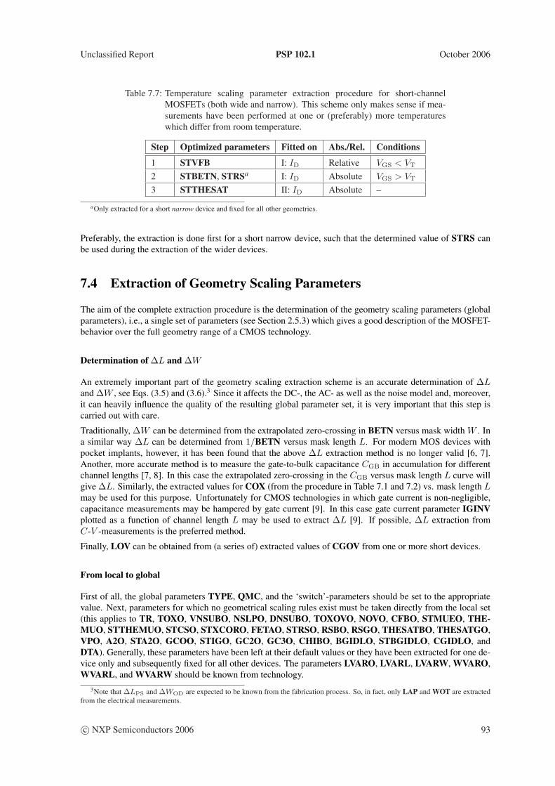
Unclassified Report PSP 102.1 October 2006
Table 7.7: Temperature scaling parameter extraction procedure for short-channelMOSFETs (both wide and narrow). This scheme only makes sense if mea-surements have been performed at one or (preferably) more temperatureswhich differ from room temperature.
Step Optimized parameters Fitted on Abs./Rel. Conditions
1 STVFB I: ID Relative VGS < VT
2 STBETN, STRSa I: ID Absolute VGS > VT
3 STTHESAT II: ID Absolute –
aOnly extracted for a short narrow device and fixed for all other geometries.
Preferably, the extraction is done first for a short narrow device, such that the determined value of STRS canbe used during the extraction of the wider devices.
7.4 Extraction of Geometry Scaling Parameters
The aim of the complete extraction procedure is the determination of the geometry scaling parameters (globalparameters), i.e., a single set of parameters (see Section 2.5.3) which gives a good description of the MOSFET-behavior over the full geometry range of a CMOS technology.
Determination of ∆L and ∆W
An extremely important part of the geometry scaling extraction scheme is an accurate determination of ∆Land ∆W , see Eqs. (3.5) and (3.6).3 Since it affects the DC-, the AC- as well as the noise model and, moreover,it can heavily influence the quality of the resulting global parameter set, it is very important that this step iscarried out with care.
Traditionally, ∆W can be determined from the extrapolated zero-crossing in BETN versus mask width W . Ina similar way ∆L can be determined from 1/BETN versus mask length L. For modern MOS devices withpocket implants, however, it has been found that the above ∆L extraction method is no longer valid [6, 7].Another, more accurate method is to measure the gate-to-bulk capacitance CGB in accumulation for differentchannel lengths [7, 8]. In this case the extrapolated zero-crossing in the CGB versus mask length L curve willgive ∆L. Similarly, the extracted values for COX (from the procedure in Table 7.1 and 7.2) vs. mask length Lmay be used for this purpose. Unfortunately for CMOS technologies in which gate current is non-negligible,capacitance measurements may be hampered by gate current [9]. In this case gate current parameter IGINVplotted as a function of channel length L may be used to extract ∆L [9]. If possible, ∆L extraction fromC-V -measurements is the preferred method.
Finally, LOV can be obtained from (a series of) extracted values of CGOV from one or more short devices.
From local to global
First of all, the global parameters TYPE, QMC, and the ‘switch’-parameters should be set to the appropriatevalue. Next, parameters for which no geometrical scaling rules exist must be taken directly from the local set(this applies to TR, TOXO, VNSUBO, NSLPO, DNSUBO, TOXOVO, NOVO, CFBO, STMUEO, THE-MUO, STTHEMUO, STCSO, STXCORO, FETAO, STRSO, RSBO, RSGO, THESATBO, THESATGO,VPO, A2O, STA2O, GCOO, STIGO, GC2O, GC3O, CHIBO, BGIDLO, STBGIDLO, CGIDLO, andDTA). Generally, these parameters have been left at their default values or they have been extracted for one de-vice only and subsequently fixed for all other devices. The parameters LVARO, LVARL, LVARW, WVARO,WVARL, and WVARW should be known from technology.
3Note that ∆LPS and ∆WOD are expected to be known from the fabrication process. So, in fact, only LAP and WOT are extractedfrom the electrical measurements.
c© NXP Semiconductors 2006 93
October 2006 PSP 102.1 Unclassified Report
Once the values of ∆L and ∆W are firmly established (as described above), LAP and WOT can be set and theactual extraction procedure of the geometry scaling parameters can be started. It consists of several independentsub-steps (which can be carried out in random order), one for each geometry dependent local parameter.
To illustrate such a sub-step, the local parameter CT is taken as an example. The relevant geometry scalingequation from Section 3.2 is Eq. (3.26), from which it can be seen that CTO, CTL, CTLEXP, and CTW arethe global parameters which determine the value of CT as a function of L and W . First, the extracted CT ofeach device in a length-series of measured (preferably wide) devices are considered as a function of L. In thiscontext CTO, CTL, and CTLEXP are optimized such that the fit of Eq. (3.26) to the extracted CT-values isas good as possible, while keeping CTW fixed at 0. Then CTW is determined by considering the extractedCT-values from a length-series of measured narrow devices. Finally, the four global parameters may be fine-tuned by optimizing all four parameters to all extracted CT-values simultaneously. The default values given inSection 2.5.3 are good initial values for the optimization procedure.
All other parameters can be extracted in a similar manner. The local parameters BETN and NEFF have quitecomplicated scaling rules, particularly due to the non-uniform doping profiles employed in modern CMOStechnologies. Therefore, a few additional guidelines are in place.
• The optimization procedure for BETN is facilitated if not BETN, but BETNsqdef= BETN · LE/WE is
considered.
• Starting from the default values, first UO, FBET1, LP1, FBET2, and LP2 should be determined from alength-series of wide devices. Then BETW1, BETW2, and WBET should be determined from a width-series of long devices. Finally, FBET1W and LP1W can be found by considering some short narrowdevices.
• Starting from the default values, first extract FOL1, FOL2, NSUBO, NPCK, and LPCK from a length-series of wide devices. Here, NSUBO determines the long-channel value of NEFF. Moreover, NPCKand LPCK determine the increase of NEFF for shorter channels (short channel effect), while FOL1 andFOL2 are used to describe the decrease of NEFF for very short channels (reverse short channel effect).
• Then NSUBW and WSEG can be determined form a width-series of long devices. Finally, NPCKW,LPCKW and WEGP are determined from a width-series of short devices.
• Especially for BETN and NEFF it is advisable—after completing the procedure described above—to finetune the global parameters found by considering all extracted values of BETN (or NEFF) simultaneously.
Note that in many cases it may not be necessary to use the full flexibility of PSP’s parameter scaling, e.g.,for many technologies NP and VFB may be considered as independent of geometry. If such a geometry-independence is anticipated, the corresponding local parameter should be fixed during local parameter extrac-tion. Only if the resulting global parameter set is not satisfactory, the parameter should be allowed to varyduring a subsequent optimization round.
Fine tuning
Once the complete set of global parameters is found, the global model should give an accurate description ofthe measured I-V -curves and capacitance measurements. Either for fine tuning or to facilitate the extractionof global parameters for which the geometry scaling of the corresponding extracted local parameters is notwell-behaved, there are two more things that can be done.
• Local parameters for which the fitting of global parameters was completed satisfactorily could be re-placed by the values calculated from the geometrical scaling rules and fixed. Then one could redo (partsof) the local parameter extraction procedure for the remaining local parameters, making them less sensi-tive for cross-correlations.
• Small groups of global parameters may be fitted directly to the measurements of a well-chosen series ofdevices, using the global model.
94 c© NXP Semiconductors 2006
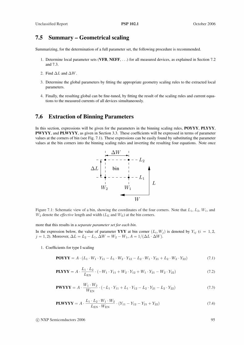
Unclassified Report PSP 102.1 October 2006
7.5 Summary – Geometrical scaling
Summarizing, for the determination of a full parameter set, the following procedure is recommended.
1. Determine local parameter sets (VFB, NEFF, . . .) for all measured devices, as explained in Section 7.2and 7.3.
2. Find ∆L and ∆W .
3. Determine the global parameters by fitting the appropriate geometry scaling rules to the extracted localparameters.
4. Finally, the resulting global can be fine-tuned, by fitting the result of the scaling rules and current equa-tions to the measured currents of all devices simultaneously.
7.6 Extraction of Binning Parameters
In this section, expressions will be given for the parameters in the binning scaling rules, POYYY, PLYYY,PWYYY, and PLWYYY, as given in Section 3.3. These coefficients will be expressed in terms of parametervalues at the corners of bin (see Fig. 7.1). These expressions can be easily found by substituting the parametervalues at the bin corners into the binning scaling rules and inverting the resulting four equations. Note once
bin
W1W2
∆W
∆L
L1
L2
L
W
Figure 7.1: Schematic view of a bin, showing the coordinates of the four corners. Note that L1, L2, W1, andW2 denote the effective length and width (LE and WE) at the bin corners.
more that this results in a separate parameter set for each bin.
In the expression below, the value of parameter YYY at bin corner (Li,Wj) is denoted by Yij (i = 1, 2,j = 1, 2). Moreover, ∆L = L2 − L1, ∆W = W2 −W1, A = 1/(∆L ·∆W ).
1. Coefficients for type I scaling
POYYY = A · (L1 ·W1 · Y11 − L1 ·W2 · Y12 − L2 ·W1 · Y21 + L2 ·W2 · Y22) (7.1)
PLYYY = A · L1 · L2
LEN· (−W1 · Y11 + W2 · Y12 + W1 · Y21 −W2 · Y22) (7.2)
PWYYY = A · W1 ·W2
WEN· (−L1 · Y11 + L1 · Y12 − L2 · Y21 − L2 · Y22) (7.3)
PLWYYY = A · L1 · L2 ·W1 ·W2
LEN ·WEN· (Y11 − Y12 − Y21 + Y22) (7.4)
c© NXP Semiconductors 2006 95
October 2006 PSP 102.1 Unclassified Report
2. Coefficients for type II scaling
POYYY = A · (L2 ·W2 · Y11 − L2 ·W1 · Y12 − L1 ·W2 · Y21 + L1 ·W1 · Y22) (7.5)
PLYYY = A · LEN · (−W2 · Y11 + W1 · Y12 + W2 · Y21 −W1 · Y22) (7.6)
PWYYY = A ·WEN · (−L2 · Y11 + L2 · Y12 − L1 · Y21 − L1 · Y22) (7.7)
PLWYYY = A · LEN ·WEN · (Y11 − Y12 − Y21 + Y22) (7.8)
3. Coefficients for type III scaling
POYYY = A · (−L1 ·W2 · Y11 + L1 ·W1 · Y12 + L2 ·W2 · Y21 − L2 ·W1 · Y22) (7.9)
PLYYY = A · L1 · L2
LEN· (W2 · Y11 −W1 · Y12 −W2 · Y21 + W1 · Y22) (7.10)
PWYYY = A ·WEN · (L1 · Y11 − L1 · Y12 − L2 · Y21 + L2 · Y22) (7.11)
PLWYYY = A · L1 · L2 ·WEN
LEN· (−Y11 + Y12 + Y21 − Y22) (7.12)
Note: For L1, L2, W1, and W2 in the formulas above one must take the effective length and width (LE andWE) as defined in Section 3.2.
96 c© NXP Semiconductors 2006
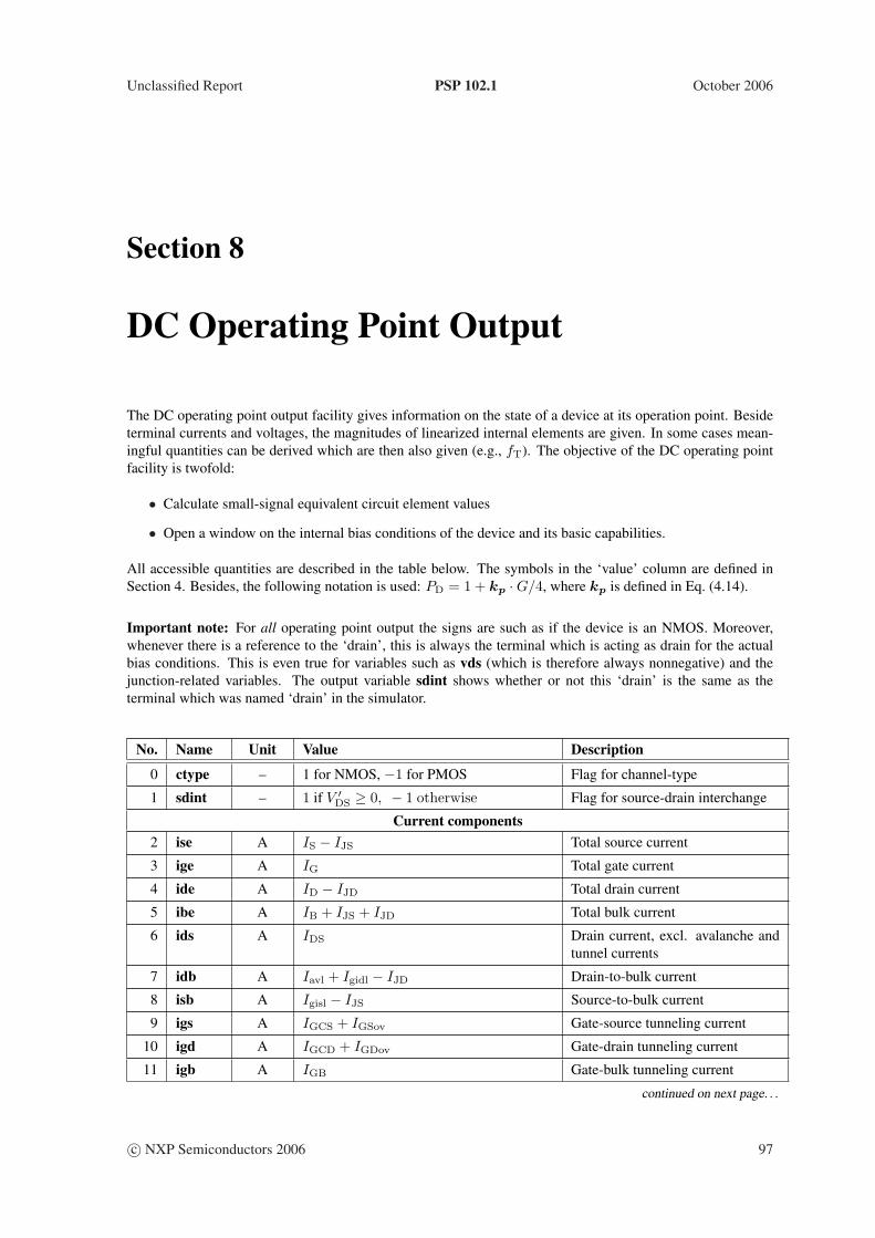
Unclassified Report PSP 102.1 October 2006
Section 8
DC Operating Point Output
The DC operating point output facility gives information on the state of a device at its operation point. Besideterminal currents and voltages, the magnitudes of linearized internal elements are given. In some cases mean-ingful quantities can be derived which are then also given (e.g., fT). The objective of the DC operating pointfacility is twofold:
• Calculate small-signal equivalent circuit element values
• Open a window on the internal bias conditions of the device and its basic capabilities.
All accessible quantities are described in the table below. The symbols in the ‘value’ column are defined inSection 4. Besides, the following notation is used: PD = 1 + kp ·G/4, where kp is defined in Eq. (4.14).
Important note: For all operating point output the signs are such as if the device is an NMOS. Moreover,whenever there is a reference to the ‘drain’, this is always the terminal which is acting as drain for the actualbias conditions. This is even true for variables such as vds (which is therefore always nonnegative) and thejunction-related variables. The output variable sdint shows whether or not this ‘drain’ is the same as theterminal which was named ‘drain’ in the simulator.
No. Name Unit Value Description
0 ctype – 1 for NMOS, −1 for PMOS Flag for channel-type
1 sdint – 1 if V ′DS ≥ 0, − 1 otherwise Flag for source-drain interchange
Current components2 ise A IS − IJS Total source current
3 ige A IG Total gate current
4 ide A ID − IJD Total drain current
5 ibe A IB + IJS + IJD Total bulk current
6 ids A IDS Drain current, excl. avalanche andtunnel currents
7 idb A Iavl + Igidl − IJD Drain-to-bulk current
8 isb A Igisl − IJS Source-to-bulk current
9 igs A IGCS + IGSov Gate-source tunneling current
10 igd A IGCD + IGDov Gate-drain tunneling current
11 igb A IGB Gate-bulk tunneling current
continued on next page. . .
c© NXP Semiconductors 2006 97
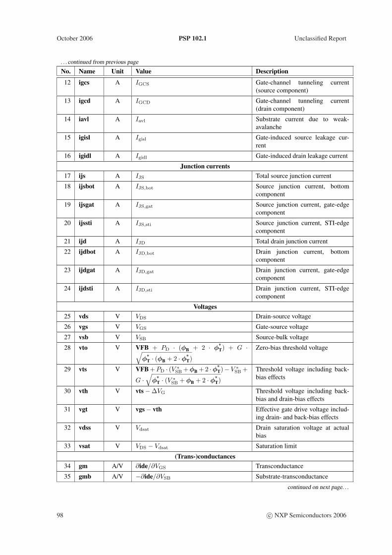
October 2006 PSP 102.1 Unclassified Report
. . . continued from previous page
No. Name Unit Value Description
12 igcs A IGCS Gate-channel tunneling current(source component)
13 igcd A IGCD Gate-channel tunneling current(drain component)
14 iavl A Iavl Substrate current due to weak-avalanche
15 igisl A Igisl Gate-induced source leakage cur-rent
16 igidl A Igidl Gate-induced drain leakage current
Junction currents17 ijs A IJS Total source junction current
18 ijsbot A IJS,bot Source junction current, bottomcomponent
19 ijsgat A IJS,gat Source junction current, gate-edgecomponent
20 ijssti A IJS,sti Source junction current, STI-edgecomponent
21 ijd A IJD Total drain junction current
22 ijdbot A IJD,bot Drain junction current, bottomcomponent
23 ijdgat A IJD,gat Drain junction current, gate-edgecomponent
24 ijdsti A IJD,sti Drain junction current, STI-edgecomponent
Voltages25 vds V VDS Drain-source voltage
26 vgs V VGS Gate-source voltage
27 vsb V VSB Source-bulk voltage
28 vto V VFB + PD · (φB + 2 · φ*T) + G ·√
φ*T · (φB + 2 · φ*
T)
Zero-bias threshold voltage
29 vts V VFB + PD · (V ∗SB + φB + 2 ·φ*
T)− V ∗SB +
G ·√
φ*T · (V ∗
SB + φB + 2 · φ*T)
Threshold voltage including back-bias effects
30 vth V vts−∆VG Threshold voltage including back-bias and drain-bias effects
31 vgt V vgs− vth Effective gate drive voltage includ-ing drain- and back-bias effects
32 vdss V Vdsat Drain saturation voltage at actualbias
33 vsat V VDS − Vdsat Saturation limit
(Trans-)conductances34 gm A/V ∂ide/∂VGS Transconductance
35 gmb A/V −∂ide/∂VSB Substrate-transconductance
continued on next page. . .
98 c© NXP Semiconductors 2006
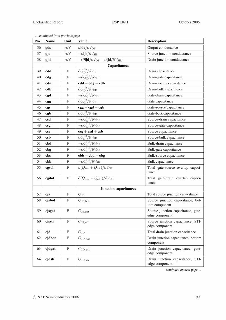
Unclassified Report PSP 102.1 October 2006
. . . continued from previous page
No. Name Unit Value Description
36 gds A/V ∂ide/∂VDS Output conductance
37 gjs A/V −∂ijs/∂VSB Source junction conductance
38 gjd A/V −(∂ijd/∂VDS + ∂ijd/∂VSB) Drain junction conductance
Capacitances39 cdd F ∂Q
(i)D /∂VDS Drain capacitance
40 cdg F −∂Q(i)D /∂VGS Drain-gate capacitance
41 cds F cdd− cdg− cdb Drain-source capacitance
42 cdb F ∂Q(i)D /∂VSB Drain-bulk capacitance
43 cgd F −∂Q(i)G /∂VDS Gate-drain capacitance
44 cgg F ∂Q(i)G /∂VGS Gate capacitance
45 cgs F cgg− cgd− cgb Gate-source capacitance
46 cgb F ∂Q(i)G /∂VSB Gate-bulk capacitance
47 csd F −∂Q(i)S /∂VDS Source-drain capacitance
48 csg F −∂Q(i)S /∂VGS Source-gate capacitance
49 css F csg + csd + csb Source capacitance
50 csb F ∂Q(i)S /∂VSB Source-bulk capacitance
51 cbd F −∂Q(i)B /∂VDS Bulk-drain capacitance
52 cbg F −∂Q(i)B /∂VGS Bulk-gate capacitance
53 cbs F cbb− cbd− cbg Bulk-source capacitance
54 cbb F −∂Q(i)B /∂VSB Bulk capacitance
55 cgsol F ∂(Qsov + Qofs)/∂VGS Total gate-source overlap capaci-tance
56 cgdol F ∂(Qdov + Qofd)/∂VDS Total gate-drain overlap capaci-tance
Junction capacitances57 cjs F CJS Total source junction capacitance
58 cjsbot F CJS,bot Source junction capacitance, bot-tom component
59 cjsgat F CJS,gat Source junction capacitance, gate-edge component
60 cjssti F CJS,sti Source junction capacitance, STI-edge component
61 cjd F CJD Total drain junction capacitance
62 cjdbot F CJD,bot Drain junction capacitance, bottomcomponent
63 cjdgat F CJD,gat Drain junction capacitance, gate-edge component
64 cjdsti F CJD,sti Drain junction capacitance, STI-edge component
continued on next page. . .
c© NXP Semiconductors 2006 99
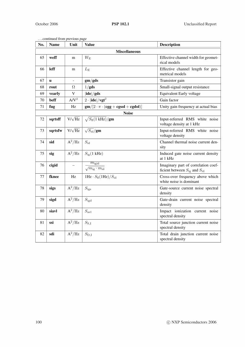
October 2006 PSP 102.1 Unclassified Report
. . . continued from previous page
No. Name Unit Value Description
Miscellaneous65 weff m WE Effective channel width for geomet-
rical models
66 leff m LE Effective channel length for geo-metrical models
67 u - gm/gds Transistor gain
68 rout Ω 1/gds Small-signal output resistance
69 vearly V |ide|/gds Equivalent Early voltage
70 beff A/V2 2 · |ide|/vgt2 Gain factor
71 fug Hz gm/[2 · π · (cgg + cgsol + cgdol)] Unity gain frequency at actual bias
Noise72 sqrtsff V/
√Hz
√Sfl(1 kHz)/gm Input-referred RMS white noise
voltage density at 1 kHz
73 sqrtsfw V/√
Hz√
Sid/gm Input-referred RMS white noisevoltage density
74 sid A2/Hz Sid Channel thermal noise current den-sity
75 sig A2/Hz Sig(1 kHz) Induced gate noise current densityat 1 kHz
76 cigid –migid√
mig ·midImaginary part of correlation coef-ficient between Sig and Sid
77 fknee Hz 1Hz · Sfl(1Hz)/Sid Cross-over frequency above whichwhite noise is dominant
78 sigs A2/Hz Sigs Gate-source current noise spectraldensity
79 sigd A2/Hz Sigd Gate-drain current noise spectraldensity
80 siavl A2/Hz Savl Impact ionization current noisespectral density
81 ssi A2/Hz SS,I Total source junction current noisespectral density
82 sdi A2/Hz SD,I Total drain junction current noisespectral density
100 c© NXP Semiconductors 2006
Unclassified Report PSP 102.1 October 2006
References
[1] L. Lemaitre, C. C. McAndrew, and S. Hamm ,“ADMS – Automatic Device Model Synthesize”, Proc. IEEECICC, 2002. See also http://mot-adms.sourceforge.net/
[2] X. Xi et al., BSIM4.4.0 MOSFET Model, User’s Manual, 2004, available for download at http://www-device.eecs.berkeley.edu/~bsim3/BSIM4/BSIM440/
[3] H. Wang, T.-L. Chen, and G. Gildenblat, “Quasi-static and Nonquasi-static Compact MOSFET ModelsBased on Symmetric Linearization of the Bulk and Inversion Charges,” IEEE trans. Electron Dev. 50(11),pp. 2262-2272, 2003.
[4] H. Wang et al., “Unified Non-Quasi-Static MOSFET Model for Large-Signal and Small-Signal Simula-tions,” CICC 2005.
[5] W. H. Press et al., “Numerical recipes in C”, 2nd edition, Cambridge University Press (1993), available fordownload at http://www.library.cornell.edu/nr/bookcpdf.html
[6] M. Minondo, G. Gouget, and A. Juge, “New Length Scaling of Current Gain Factor and CharacterizationMethod for Pocket Implanted MOSFET’s,” Proc. ICMTS 2001, pp. 263-267, 2001.
[7] A.J. Scholten, R. Duffy, R. van Langevelde, and D.B.M. Klaassen, “Compact Modelling of Pocket-Implanted MOSFETs,” Proc. ESSDERC 2001, pp. 311-314, 2001.
[8] T.S. Hsieh, Y.W. Chang, W.J. Tsai, and T.C. Lu, “A New Leff Extraction Approach for Devices with PocketImplants,” Proc. ICMTS 2001, pp. 15-18, 2001.
[9] R. van Langevelde et al., “Gate Current: modelling, ∆L Extraction and Impact on RF Performance,” IEDM2001 Tech. Digest, pp. 289-292, 2001.
c© NXP Semiconductors 2006 101
October 2006 PSP 102.1 Unclassified Report
Appendix A
Auxiliary Equations
In this Appendix, some auxiliary functions which are used in the model equations are defined.
The MINA-smoothing function:
MINA (x, y, a) =12·[x + y −
√(x− y)2 + a
](A.1)
The MAXA-smoothing function:
MAXA (x, y, a) =12·[x + y +
√(x− y)2 + a
](A.2)
The functions χ(y), its derivatives, σ1, and σ2, which are used in the explicit approximation of surface potential:
χ(y) =y2
2 + y2(A.3)
χ′(y) =4y
(2 + y2)2(A.4)
χ′′(y) =8− 12y2
(2 + y2)3(A.5)
ν = a + c (A.6)
µ1 =v2
τ+
c2
2− a (A.7)
σ1 (a, c, τ, η) =a · ν
µ1 + (c2/3− a) · c · ν/µ1+ η (A.8)
µ2 =v2
τ+
c2
2− a · b (A.9)
σ2 (a, b, c, τ, η) =a · ν
µ2 + (c2/3− a · b) · c · ν/µ2+ η (A.10)
102 c© NXP Semiconductors 2006