OCK 2017 - RICH LTD...Oceanside, CA 92056 Telephone: 760-722-2300 Toll Free: 800-325-5538


PSI-ER-5538-03
The views and conclusions contained in this document are
those of the authors and should not be interpreted as
representing the official policies, either expressed or
implied, of the Defense Advanced Research Projects Agency
or the U.S. Government.
1) d
I. it
LI

PSI-ER-5538-03
TABLE OF CONTENTS
Section Title Page
EXECUTIVE SUMMARY ....... ....................... v
1 INTRODUCTION ..... .... ........................ 1-1
2 PROM DESCRIPTION ..... .. ...................... .. 2-1
3 OPTICAL TEST LAYOUT ....... ..................... 3-1
4 EXPERIMENTAL DATA ...... ...................... . 4-1
4.1 Optical Quality of the PROM ................... 4-14.2 The Acousto-Optical Modulator Illumination and the Fourier
Transform Plane Intensities .... ................. 4-34.3 Frequency Response with a Single Tone Excision Notch . ... 4-94.4 Single Frequency Input Versus Output Power .......... 4-134.5 Excision with Wideband Noise Plus Narrowband Interference .. 4-154.6 Excision with No Blue Write Light.... ... .... ... 4-174.7 Correlation with a Jamming Signal and Optical Excision . 4-204.8 Excision of Narrowband Interference from a Pulsed Signal 4-22
5 PROM CONCLUSIONS ........ ....................... 5-1
6 PHOTODICHROIC DESCRIPTION .... .................. ... 6-1
6.1 Introduction ..... ... .. ........................ 6-16.2 Optical Attenuation ................................ 6-36.2.1 Measurements With Uniform Illumination .. ........... .. 6-46.2.2 Measurements With Diffracted Signal Illumination ... ...... 6-8
7 SPREAD SPECTRUM MEASUREMENTS .... ................ ... 7-1
7.1 Test Equipment ..... ... ....................... 7-17.2 Experimental Data ...... ...................... . 7-3
8 PHOTODICHROIC CONCLUSIONS .... .................. ... 8-1
9 PHOTOCHROMIC GLASSES ... ........................ 9-1
10 OPTICAL CLIPPER CONCLUSIONS .... ................. .. 10-1
lii
'I i .. ...... ..

PSI-ER-5538-03
LIST OF ILLUSTRATIONS
Figure Title Page
2-1 PROM Construction ...... .. ...................... 2-2
2-2 Plot of IROut = IR si2 Z exp(-IR/I) ... ............ .. 2-7
3-1 Optical Layout for the PROM Experiments .... ........... 3-2
4-1 RF Pulse Input and Output .... .................. ... 4-2
4-2 Acousto-Optic Aperture Illumination ... ............. . 4-4
4-3 Test Configuration for Measuring the AO System FrequencyResponse with a Single Frequency Excision Notch ... ....... 4-10
4-4 Frequency Response with a Single Tone Excision Notch . . .. 4-11
4-5 Frequency Excision Using an Optically Opaque Wire in thePROM Acousto-Optic System .... .................. ... 4-12
4-6 Experimental Data for PROM Clipping Characteristics with aSingle Frequency Input and a Blue Write Time at At = 0.3 Sec 4-14
4-7 Excision with Wideband Noise Plus a Single Frequency forthe Input ....... .......................... . 4-16
4-8 Detected Output Magnitude Versus Time for a Single FrequencyInput with No Blue Write Light in PROM Cycle ... ........ 4-19
4-9 Probability of Detection for 127-Bit Digital Correlator as aFunction of J/S with Input SNR = -4 dB .. ........... .. 4-21
4-10 Excision of Narrowband Interference from a Pulsed Signal . 4-23
5-1 Envisioned Real-Time Device for Optical Excision ... ...... 5-3
6-1 Photodichroic Crystal at the Transform Plane of anOptical Spectrum Analyzer .... .................. ... 6-2
6-2 Attenuation Test Setup for Uniform Illumination ... ....... 6-5
6-3 Photodichroic Crystal -- Insertion Loss Vs. Exposure Timefor 13 mW/cm 2 Incident Optical Power ..... ............ 6-6
6-4 Photodichroic Crystal -- Insertion Loss Vs. Exposure Timefor 130 mW/cm2 Incident Optical Power ... ............ .. 6-7
6-5 Coherent Signal Processor with Optical Clipper atTransform Plane ...... ....................... .. 6-9
7-1 Electronic Setup for Broadband Test ... ............. ... 7-2
8-1 Optical Scattering by the Photodichroic Crystal ......... .. 8-3
9-1 Photochromic Glass Test Setup ...... ................ 9-2
9-2 Attenuation as a Function of Time for Photochromic Glass 9-3
iv

PSI-ER-5538-03
EXECUTIVE SUMMARY
The ability to significantly reduce the vulnerability of broadband
receivers to narrowband jammer interference has been successfully demonstrated in
the laboratory. The interference signal levels were attenuated by the self-adaptive
frequency selective limiting properties of an optical processor invented by PROBE
SYSTEMS, INC. This report describes the evaluation of optical clipper materials that,
when placed in the optically-generated spectrum of a broadband RF signal, would
selectively attenuate narrowband signals. The three optical clippers that were
evaluated were: (1) a PROM developed by Itek Corporation and supplied by Naval
Research Laboratory, (2) a selection of photodichroic crystals developed and
supplied by Naval Research Laboratory, and (3) a photochromic glass purchased
from Corning.
The most successful results were obtained with an optical memory
developed by Itek and named the PROM. This device, when exposed to narrowband
signals, affects the polarization of the transmitted light and at the same time
passes those portions of broadband signals not covered by narrowband signals.
By coherently detecting the transmitted light, the optical processor continuously
reconstructs the broadband signals without the interference that could have
degraded or even prevented further signal processing or display.
Experimental results included a test where a simulated spread spectrum
radar return with a 20-MHz bandwidth was buried in noise by 4 dB. The detection
probability of this signal after passing through a digital matched filter was
90% when the threshold was adjusted for less than a 10-6 false alarm rate.
When a narrowband jamming signal was introduced at increasingly higher power
levels, the detection probability would fall -- for example, at a jammer-to-
signal ratio of 9 dB, the probability of detection was only 1%. When the optical
signal excisor was inserted just before the digital matched filter, the probability
of detection rose to almost 80%. Even at a jammer-to-signal ratio of 24 dB, the
probability of detection was 50% when the excisor was used as part of the radar
processor system. Spectrum analysis showed that the excisor reduced the jammer
level by as much as 27 dB, almost down to the receiver noise level.
v

PSI-ER-5538-03
The analytical and experimental results described in this report
provide clear evidence of the potential benefits that could be realized by placing
an optical signal excisor in receivers used in broadband radar, communication,
and intercept systems. Future investments in the optical clipper should be
concentrated on the development of a PROM-like optical device that can continu-
ously respond to the signal environment, that can be fabricated to have higher
resolution, and that can be operated with considerably less support equipment.
Device development work combined with PROBE's system-level analytical and
experimental investigations would greatly expedite the transfer of signal excision
technology to users now facing an increasingly complex electronic signal environment.
Ivb.,

PSI-ER-5538-03
SECTION 1
INTRODUCTION
This special technical report describes the results of a task
conducted by PROBE SYSTEMS as part of a DARPA/NAVELEX Joint Program for Optical
Excision. The purpose of this task was to experimentally evaluate the feasibility
of using optical addressed spatial light modulators to adaptively excise
narrowband signals from spread spectrum signals. This work resulted in the
successful demonstration of an optical excisor with an Itek PROM used in the
front end of a simulated spread spectrum radar operated in the presence of a
narrowband jammer. The attenuation effects of the PROM against the jammer
reduced the jammer level and improved the probability of detection from 1% to
80% and permitted 50% detection probability even when the jammer was 24 dB
stronger than the signal.
Optical excision is a signal processing technique for eliminating
narrowband RF interference signals and has many potential applications in the
areas of broadband communications, radar, and intercept systems. This technique
uses an acousto-optical Bragg cell and a continuous laser to spatially form the
signal spectrum of an electrical input. By blocking strong narrowband interference
signals in the optically-generated signal spectrum and by coherently detecting
the remainder of the spectrum, an interference-free electronic broadband signal
is obtained as the output of the processor. The successful development of
optical excisor technology will permit the exploration of a whole family of
optical coherent processors that, in real-time, will allow access to the
spectrum of a broadband signal.
Considering all of the candidate clippers for use in the coherent
processor, the PROM offers many advantages. However, this device has been
developed to serve as an optical memory, e.g., an electronic transparency.
What is really needed in the excisor is a self-adaptive transparency that
continuously responds to the incident signal spectrum. This mode of operation
should also greatly simplify the support electronics and permit the development
of a rack-mounted excisor.
V 1-1
t

PSI-ER-5538-03
SECTION 2
PROM DESCRIPTION
The Itek PROM is an optical device which is intended to be used
as a two-dimensional, optical image storage medium. In normal use, the PROM
is electronically cycled between an optical record and an optical readout
stage so that the PROM acts like a real-time optical transparency. During the
record stage, the PROM is "exposed" to an optical intensity image consisting
of blue light such that this image is spatially stored in the PROM. During
the readout stage, the PROM is illuminated with a red optical beam such that
the stored image spatially modulates the optical transmittance of the red beam.
Thus the net red image obtained is the product of the incident red beam times
a stored image modulation function.
The physical construction of the PROM is shown in Figure 2-1. Th-e key
element of the PROM is an electro-optic, photoconductive crystal of Bi12SiO 20 .
For the Itek PROM, this crystal is 800 urm thick and 1 inch in diameter. The
crystal is sandwiched between insulating layers of parylene and transparent
electrodes such that the PROM acts as a simple capacitor when no optical
illumination is present. If the PROM is erased of all previous images and
a voltage is placed across the transparent electrodes, an electric field will
appear across the Bi12Sio 20 crystal. Then if one illuminates a particular
position of the PROM with a blue optical beam, the photoconductivity of the
crystal causes electronic charges to be locally generated at that position.
Due to the electric field across the crystal, these charges migrate to parylene-
crystal interface so that the voltage drop across the crystal is decreased
while the voltage drop across the parylene layers is increased. With enough
optical illumination, the voltage across the crystal is reduced to zero. Since
the charge migration is spatially dependent on the optical illumination of the
blue beam, one can spatially control the voltage drop across the crystal of
Bi12Sio 20 with the blue beam.
2-1
L

PSI-ER-5538-03
PARYLENEINSULATOR
TRANSPARENTlo ELECTRODES
B12~ i 20
CRYSTAL
ELCRD0 LCRD
FIUE21 POMCNTUTO
02-

PSI-ER-5538-03
2. Continued
The photoconductivity of the crystal is most sensitive to optical
illumination in the blue portion of the optical spectrum. For a given optical
exposure of E, the voltage across the crystal will decay exponentially by the
factor exp(-E/Eo) due to the photoconductivity. The quantity E0 is the I/e decay
exposure and is a function of optical wavelength. For an optical wavelength0
of 4880 A corresponding the blue line of an argon laser, E0 = 40 ergs/cm 2. For0
an optical wavelength of 6328 A corresponding to the red line at a helium-neon
laser, E0 104ergs/cm2. Thus for equal intensity illumination of the Bi12Si0 20
crystal with these optical wavelengths,the blue illumination will cause the
voltage across the crystal to decay 250 times as fast as the red illumination. 4In the readout mode, the electro-optic properties of the Bi12SiO 20
crystal are utilized to modulate the polarization of a red optical readout beam.
This polarization modulation is then converted to an optical intensity modulation
using a polarizer. For the particular PROM utilized, the transmission mode for
polarization modulation was most optically efficient. In this mode, an incident
red optical beam with linear polarization is transmitted through the PROM. With
no voltage across the crystal, the transmitted red beam will undergo a constant0polarization rotation of roughly 18 due to the optical activity of the crystal.
Thus the exit red beam with no voltage across the crystal is linearly polarized.
With a voltage across the crystal and the crystal properly oriented, the electro-
optical effect will act to change the exit polarization. To convert this
polarization change to an optical intensity modulation, one typically orients
the exit polarizer such that with no voltage across the crystal, the polarizer
blocks the exit light. Then with a voltage V across the crystal, the effective
optical intensity modulation T is given by:
T = Tosin2(V()
For the PROM utilized, VH 3900 volts and is termed the half-wave voltage.
2-3
_ . -- -- --- -

PSI-ER-5538-03
2. Continued
With the foregoing information, one can now consider the complete
PROM record/readout cycle. The first step of the record stage is to erase
all the previous stored image patterns in the PROM using a spatially uniform
flash of blue light obtained from a flashlamp. This blue light flash makes
the Bi 12Sio20 crystal uniformly photoconductive so that a uniform spatial
charge distribution across the device is developed. The second part of therecord stage is to place a voltage V0 across the PROM and illuminate the PROM
with the desired blue light image for a time duration tt. With a blue light
image intensity distribution given by I(x,y), this record procedure will
produce a spatial voltage distribution across the Bi12SiO 20 crystal given by:
V(x,y) : V0 exp [IB(X,y) At/EoB] (2)
In this expression, EOB is the 1/e decay exposure for the blue image write beam.
This completes the record stage. The optical readout stage is performed by
illuminating the PROM with a red optical beam whose optical intensity distribution
can be described by IR(xy). The net effective red beam intensity IRout transmitted
through the PROM-exit-polarizer combination is then given by:
IRout : IR(xy) T(x,y) (3)
Since T(x,y) can be obtained by combining Equations 1 and 2, the expanded version
of Equation 3 takes the form:
IRu IR '~ in 2 I Vo y)At 4:Rout R(x'y) s 1nL exp [.-IB(X~y) At/EoB - (4)
2-4
PSI-ER-5538-03
2. Continued
Typically the voltage V0 is set approximately equal to VH to allow a maximum
on-off contrast ratio. One can see from equation 4 that if the blue write
beam has a high intensity at a particular position ()0,yo), then the red beam
will be highly attenuated at that position.
Actually, Equation 4 is an approximation in that it does not
include the effect of the red read beam'causing photoconductivity in the crystal
and writing an image of itself. Thus as time progresses, the exit red beam
IRout(xy) is gradually attenuated. This attenuation is most rapid at the
portions of input red beam that are most intense. To account for this effect,
Equation 4 can be modified to:
V1'Rout : IR(X'Y) sin2 exp (-) (5A)
a I B(xy) At/EOB + IR(X,y)(t-to)/EOR (5B)
,t to
In Equation 5B, the quantity At represents the exposure time of the blue beam
as before while the quantity t-tO represents the exposure time of the red beam
which starts at the beginning of the read stage at time to. The quantity EOR
represents the i/e decay exposure level for the red beam. Since EOR 250 EOB,
the red beam exposure creating self-attenuation of the red readout beam is usually
not significant unless the red exposure IR(t-to) is approximately 250 times
greater than the blue exposure IB At.
iB
2-5
\

PSI-ER-5538-03
2. Continued
For PROBE's application of employing the PROM as an optical
clipper, the blue write beam has an optical intensity distribution which isapproximately (if one ignores the red reference beam intensity) proportional
to the red readout beam intensity:
IB(xy) = K IR(xly) (6)
In this equation, K is a constant of proportionality. Plugging Equation 6 into
Equations 5A and B, one has for the red readout beam intensity IRout in the
optical clipper mode:
IRout(X,y) = IR(xy) sin 2 2VH exp (-IR(X,y)/i) (7A)
I A KAt t-tot t (7B)-EOB EOR
One can plot IRout versus IR as is done in Figure 2-2 with logarithmic coordinate
scales and with V0 = VH. One can see that for a fixed 1, IRout is linearlyrelated to IR for IR somewhat less than I, while for IR somewhat greater than I,IRu decreases very rapidly. The maximum value of IRout/I is 0.347 and occursIRout Ru
at IR/I = .65. Thus it is convenient to label I as the optical clipping threshold.
Note that for longer exposure times on either the blue or red beams, the clipping
threshold I decreases.
The preceding discussion of the PROM has ignored a number of possiblealternatives for modes of operation. For example, one has the option of adding
a spatially uniform baseline subtraction voltage to the spatial voltage distribution
described in Equation 2. Also, one can consider other orientations of the exit
2-6

PSI-ER-5538-03
11
0.347
10-3 _
(' -10 *
.0
0co
10-3 10-2 10-1 1 10IR/1
FIGURE 2-2 PLOT OF IRout I R sin 2[ exp(-IR/I)
2-7
PSI-ER-5538-03
2. Continued
polarizer. These options can produce some interesting effects for the optical
clipper application, but have the problem of not having a large attenuation
for very high exposures with the write light. For this reason, these options
were avoided. Also, it should be apparent from the previous discussion that it
is not necessary to use any write illumination on the PROM to utilize it as an
optical clipper since the read beam acts to expose the PROM and causes self
clippling. This mode of operation where the PROM is cycled with no write
light will produce a clipping threshold I which decreases with time from the
start of the read stage at t =to
E t t t (8 )
t-t0
The value of E is a function of the read light optical wavelength as before,
but for this mode, the read light is not necessarily red. Plugging Equation
8 into Equation 7A, one has for the exit readout beam optical intensity Iout
as a function of the input read beam intensity In with no write light:
I XY = ~I (xy) sin21j!- exp -In(x ,y)(t-t0)/E0o(9
The basic properties of Equation 9 are similar to those of Equation 7A except
that there is always a time delay from the start of the read cycle before I
becomes small enough to create optical clipping. Once should note that the
exponential time delay rate in Equation 9 is proportional to the input read
beam intensity fin. Thus strong optical signals are attenuated more rapidly
than weak optical signals for the mode of operation where no write illumination
is used.
2-8

PSI-ER-5538-03
SECTION 3
OPTICAL TEST LAYOUT
The optical test layout for obtaining data in the PROM experiments
is shown in Figure 3-1. This layout utilizes two separate lasers to produce the
red (Hughes 5 mW HeNe laser at 6328 A) and blue (Spectra-Physica 2 mW Argon laser
at 4880 A) light. One can think of the optical layout as consisting of separate
red and blue optical systems which share some optical components. The red
system consists of a PROBE SYSTEMS' coherent-detection, acousto-optic system
using a Mach-Zehnder interferometer. The red system generates a signal beam in
one path of the interferometer by passing the red light through beam expansion/
collimation optics, an acousto-optic modulator, and a Fourier transform lens.
A red reference beam is generated in the other path of the inter-
ferometer and combined with the red signal beam via a beam splitter. The combined
red signal and reference beams are then passed through the Itek PROM, which is
located in the Fourier transform plane of the acousto-optic modulator. This
combined red beam acts as the optical readout beam for the PROM and is guaranteed
to be linearly polarized by the use of a polarizer before the PROM. After passing
through the PROM, the red readout beam is passed through a crossed polarizer and
focused onto a photodetector to produce the coherent RF output.
All of the red light passing through the PROM is incident on thephotodetector surface so that any phase perturbations produced by the PROM have
no effect on the signal output. If one removed the PROM and the crossed polar-
izer, the red systemwouldbe the same as a conventional coherent-detection,
acousto-optic system with image plane detection.
As in most other experiments, the photodetector used was the
Varian VPM 152-D, which has a bandwidth of 2 GHz. The acousto-optic modulator
used was the Anderson Laboratories BD-125, which has a bandwidth of 25 MHz
centered at 40 MHz and a time-bandwidth product of 125 for rectangular window
Illumination. For the PROM experiments, the illumination was closer to Gaussian.
The details of the acousto-optic cell illumination and the Fourier transform spot
size are further discussed in the experimental data section.
3-1

PSI - ER- 5538-02
VI-
Ljj
uLi
04 -1
0:0
C>~
V)JL 00nc
0 C)
C) Li)
cc . L
Li.0 cc -J
< >
0i LL.r-
LIC 0) of)
-JJSalj
CD, ce m3-2CD C3
m co C C

PSI-ER-5538-03
3. Continued
The blue optical system is used to obtain an image of the RF input
signal spectrum which can then be used to write on the PROM during the write
stage of the PROM cycle. To do this, the blue beam from the argon laser bounces
off the beam splitter and passes through the beam-expansion/collimation optics,
the acousto-optic modulator, and the Fourier transform lens in a manner similar
to the red signal beam. The blue signal beam then bounces off the second beam
splitter and passes through an optical path which acts to magnify and image the
blue Fourier transform plane onto the reverse side of the PROM. This magnification
is necessary to match the blue spatial Fourier transform to the red signal beam
Fourier transform because the size of the spatial Fourier transform is proportional
to wavelength. Thus the blue Fouriertransform must be magnified by the factor
6328/4880 = 1.30.
In order to have the blue Fourier transform match spatially with
the red Fourier transform, very fine positioning to within ±25 micrometers
for the blue beam is required. This positioning was obtained by micrometer
screw adjustments which controlled the tilt of the blue beam mirrors. One
should note thatthe blue optical system is separated from the red by use of"redpass" and bluepass" apertures. This is possible because the red and blue
beams are not exactly collinear and are tilted with respect to each other in
a direction out of the page in Figure 3-1. The tilt between the red and blue
beams is such that they coincide when passing through the acousto-optic
modulator but are separate at significant distances from the acousto-optic
modulator.
One should also note in Figure 2-2 that the blue reference beam is
blocked so that only the blue signal beam is used for writing on the PROM.
Finally, one should note that electronically-controlled shutters are used to
alternately select the blue and red lasers for the record and readout stages
of the PROM cycle.
*3-3
Lai°

PSI-ER-5538-03
SECTION 4
EXPERIMENTAL DATA
A considerable number of experimental measurements were performed to
examine the capabilities of the PROM as an optical clipper. One should keep in
mind when examining this data that the PROM is a storage device so that all data
written on the PROM remains stored until the next erase/record stage of the
PROM cycle. Thus tht Itek PROM is not a true real-time device in the sense
that it must be continually cycled through the erase/record and read cycles.
4.1 OPTICAL QUALITY OF THE PROM
One of the first characteristics of the PROM which was examined before
procedding with the optical clipping experiments was its optical quality. By
passing the red reference beam through the PROM with no polarizers and then
magnifying and examining the exit red beam, one could see the beam distortion
caused by the PROM. While the incident red reference beam was a smooth looking
line at roughly 1 millimeter in width and 20 millimeters in length, the exit red
beam was jagged and had a number of gaps in it corresponding to dirt specs on the
PROM. After considerable positioning, a location on the PROM was found which had
a mild amount of distortion. This location was used for subsequent experiments.
Unfortunately, the exposed PROM surfaces could not be cleaned because they were
comprised of the unprotected and soluble transparent electrodes.
To examine the effects of the PROM's optical distortion on the
coherent-detection output, the output of the optical system was extamined for an
RF pulse input. The input RF pulse is shown in Figure 4-1A and consists of approx-
imately nine cycles of a 40-MHz sine wave with a 14.5 volt peak-to-peak amplitude.
This signal level represents roughly a 40% diffraction efficiency for the acousto-
optic modulator. The coherently detected output pulse with the PROM physically
removed from the optical system of Figure 3-1 is shown in Figure 4-1B. Notice
that even without the PROM there is significant distortion in the form of after
* -4-1
( 1

PSI-ER-5538-03
4.1 Continued
pulse ringing. This ringing is believed to be due to an optical reflection
created by a non-antireflection coated cylindrical lens for the beam expanding
optics. This optical reflection is further examined in Section 4.2, which
discusses the acousto-optic modulator illumination. The PROM was then inserted
into the optical system of Figure 2-2 with no voltage across the PROM and the
exit polarizer not crossed. In this mode, the PROM should have no spatial
modulation and not affect the coherent detection output. The coherently detected
output pulse with the PROM in this mode is shown in Figure 4-IC. Comparing
Figures 4-1B and 4-1C, one sees that the PROM does not significantly affect the
coherently detected output despite its mild beam distortion. There is, however,
a small amount of distortion created which is evident from the difference in
after pulse ringing between Figures 4-1B and 4-IC.
One final optical characteristic of the PROM involves its optical
attenuation in the transmission mode. With no exit polarizer, the PROM attenuates
the transmitted beam intensity to approximately 50% of the input beam intensity.
This high amount of attenuation is believed to be caused by the optical index
of refraction mismatches between the adjacent layers of the PROM.
4.2 THE ACOUSTO-OPTIC MODULATOR ILLUMINATION AND THE FOURIER TRANSFORMPLANE INTENSITIES
To avoid the sidelobes in the spatial Fourier transform plane which
are associated with uniform spatial illumination of the acousto-optic modulator,
the illumination of the acousto-optic modulator aperture was made nearly Gaussianin the direction of the sound propagation. The illumination immediately after
the acousto-optic modulator aperture was experimentally measured using a narrowrazor blade slit attached to the front of an NRC photodetector head which was
in turn mounted on a linear translation stage. This measured illumination intensity
is plotted in Figure 4-2. The total width of the acousto-optic modulator aperture
is 20.6 millimeters so that one can see from Figure 4-2 that nearly the entire
4-3

PSI-ER-5538-03
RELATIVE INTENSITY
1.0In*
co
S10 -5 0 5 .lo
o /Nto iI
DITAC (o.)
l4-4
/I
I
/s.
I----------------------10 -50 5 1
DITNE(m
FIUE42AOSOOTCAETR LU/NTO
4-

PSI-ER-5538-03
4.2 Continued
signal beam was contained within this aperture. Actual data was taken only
for x 0 due to the limits of the translation stage movement. The data
shown as a dotted line for x < 0 is actually a reflection of the data for
positive values of x. This is a reasonable approximation due to the symmetry
of the signal beam illumination. Note that there is some "ripple" in the
illumination intensity near the edges of the acousto-optic modulator aperture.
This ripple appears to be created by a double reflection of the optical signal
beam off the surfaces of the non-antireflection coated cylindrical lens used
for the signal beam expansion. This reflection cannot be eliminated by tilting
the lens, so that the only cure appears to be to use anti-reflection coated
cylindrical lenses for the optical beam expansion. This approach will be tested
at a future date on another contract, but is not reported here. As previously
mentioned, this double reflection is the suggested cause of the after pulse
ringing of Figures 4-1B and 4-IC.
By examining Figure 4-2 one can calculate the effective time--bandwidth
product of the acousto-optic modulator for the acousto-optic window illumination
uscd. The half-power intensity width of the illumination is seen to be approximately
7.5 millimters while the I/e2 intensity width is approximately 13 millimeters.
To calculate the effective time-bandwidth product, one should use optical
amplitude because the diffracted signal beam amplitude is proportional to the
input electrical signal amplitude. Since the time-bandwidth product of the
acousto-optic modulator with full aperture, uniform illumination is 125 and the
full aperture width is 20.6 millimeters, the3dB amplitude time-bandwidth product
is given by (7.5/20.6) x 125 46 while the 1/e amplitude time-bandwidth product
is given by (13/20.6) x 125 79.
It is useful to estimate the optical intensity distribution on the
PROM surface. The PROM is located in the spatial Fourier transform plane at the
acousto-optic modulator so that a single frequency input signal to the modulator
will create an optical signal beam amplitude distribution on the PROM which is
4-5

PSI-ER-5538-03
4.2 Continued
the spatial Fourier transform of the acousto-optic modulator optical amplitude
illumination. From this one can calculate the intensity distribution ISR(xy)
at the red signal beam at the PROM surface. Assuming that the illumination of
Figure 4-2 is approximately Gaussian with a l/e amplitude width of 13 millimeters,0
and taking into account the optical wavelength (6328 A) and the focal length
of the Fourier transform lens (48"), one has for the red signal beam intensity:
_ _y__ 2 _/ x-xoI R(x'y) (OZ) KR .(1)2 e(x-x02 (10)
In this equation DE represents the first order diffraction efficiency, KR is a
constant of proportionality, and distances x and y are in centimeters. The
variable x is proportional to frequency and represents the center location of
the diffracted signal beam spot. The 1/e optical intensity width in the y
direction at 0.2 centimeters is obtained from a rough visual estimate while
the l/e intensity width in the x direction at .0054 centimeters is calculatud*
from a spatial Fourier transform of the measured illumination of Figure 4-2.
To obtain the constant Kr; the total first order diffraction optical powerhitting the PROM was measured as being 57.,1- at a diffraction efficiency of
12%. Integrating equation 10 over x and y and equating the result to 57W, one
can solve for KR and obtain:
22
ISR(x,Y) (10011)(5) Watts (1cm
J*. Randolf and J. Morrison, "Rayleigh-Equivalent Resolution of Acousto-opticDeflection Cells," Applied Optics, Vol. 10, No. 6, p. 1453, 1971.
4-6

PSI-ER-5538-03
4.2 Continued
Similar measurements were performed for the blue optical signal beam to obtain
a first order diffraction signal beam intensity distribution ISB(x,y) of the
PROM surface for a single frequency input signal of:
IsBX (Y DE (.1O)e(0) e(00027 Wattsi C%) ecm 2 (12)cm
Note that the spatial distribution of the blue beam matches that of the red
beam as intended. Also, the blue beam is 5.6 times less intense than the
red beam.
Finally, the intensity of the red reference beam IRR(x,y) at the
PROM surface was also measured in a manner similar to the above estimates. The
result is:
IRR(X,y) (1.5 x 10⁴) e- Watts (13)cm2
As before, the l/e intensity width at 0.14 centimeters in the y direction was
obtained by a visual estimate.
Using Equation 13, the maximum exposure per square centimeter for the-4 2
red reference beam for a 5-second period is given by 7.5 X 10 joules/cm-3 2Using the l/e voltage decay exposure of 10 joules/cm for the PROM at 6328 A
(as quoted by Itek), this predicts a maximum voltage decay at e - ' 7 5= .47 due to
the reference beam after 5 seconds of exposure. In actual experimentation with
4-7

PSI-ER-5538-03
4.2 Continued
the blue write beam blocked and a low-level, broadband signal input which
produced an optical signal beam intensity much weaker than the red reference
beam intensity, the detected signal decayed to approximately 60% of its
original amplitude after 5 seconds from the start of the read stage. This decay
is due to the red reference beam and is in moderatelyclose agreement with thedecay to sin2[F(.47)]x 100,= 45% which is predicted by the above calculation.
L2The moderate difference between the experimental result and the predictedresult can be at least partly attributed to the fact that the prediction was
for the maximum amount of voltage decay at the center of the gaussian in Equation
13 as opposed to an "average" decay over the entire reference beam width which
occurs in the experimental measurement.
For time periods much less than 5 seconds, the red reference beam
causes negligible voltage decay across the PROM so that the voltage decay is
dominated by the red and the blue signal beams. One can formulate the peak
voltage decay across the PROM for a single frequency input with a blue exposure
time of (t-t0) seconds using the fact that the 1/e decay exposures for red
and blue are 10 and 4 x 10 joules/cm respectively. The peak exposure
occurs at y = 0 and x = x0 so that from Equations 11 and 12 one can derive:
____ ) t (.56) (t -t)
Peak Voltage Decay =e _ ](4Xlo6 i0- j (14)
-(DE 25,00OAt + 56 I.t)
t << 5 seconds
4-8

PSI-ER-5538-03
4.2 Continued
Thus with the blue write beam blocked, a single frequency diffraction efficiency
of 0.18% should create a l/e peak voltage decay after (t-to) = 1 second due to
the red signal beam. Similarly, with a single frequency diffraction efficiency
of 0.004%, the blue beam should create a 1/e peak voltage decay after a blue
exposure time At = 1 second.
4.3 FREQUENCY RESPONSE WITH A SINGLE TONE EXCISION NOTCH
One experiment which was performed to examine the PROM for its
capabilities as an excisor of narrowband interference was to use a single frequency
tone for the input signal during the write signal stage of the PROM cycle and
then use a network analyzer to measure the acousto-optic system's RF frequency
response during the read stage. The test configuration for this set of measurements
is shcwn in Figure 4-3. During the write stage, the acousto-optic system's RF input
is switched to a single frequency input at 40 MHz which generated an acousto-optic
modulator input level of 8 volts peak to peak or a 12.1% first order diffraction
efficiency. This single tone during the write stage will cause the blue write
beam to expose a spot on the PROM and create a frequency excision notch at
40 MHz. During the read stage, the acousto-optic system's RF input was switched
to an HP 8505A network analyzer which displayed the system frequency response on
a CRT. The signal level of the frequency chirp used by the network analyzer was
at a low level to prevent any decay of the PROM voltage caused by the red read
signal beam. A series of photographs of the system frequency response during the
read stage were taken for several blue write time durations At. These photographs
are shown in Figures 4-4A through D, where At = 0.05, 0.15, 0.3, and 0.6 seconds
for A, B, C, D, respectively. Larger values at At did not create any significant
change in the excision notch depth so that At = 0.3 seconds appeared to be a long
enough time duration to achieve a maximum excision depth (approximately 30 dB).
For comparison purposes, an optically-opaque wire was placed in the Fourier trans-
form plane to act as an excision notch. The frequency response with this wire
excision is shown in Figure 4-5. Note that even with a perfectly opaque, moderately
thick wire, it was not possible to obtain an excision depth greater than 42 dB.
4-9

PSI-ER-5538-03
SINGLE FREQUENCYSIGNAL GENERATOR
40 MHz
t - - W R I T E F I P TA C O E N -DETECTION SYSTEM RFOT T
WITH PROM
REA
OD
HP 8505A________ ___
NETWORK ANALYZER
FIGURE 4-3TEST CONFIGURATION FOR MEASURING THE AO SYSTEM
FREQUENCY RESPONSE WITH A SINGLE FREQUENCY EXCISION NOTCH
4-10


PSI-ER-5538-03
4.3 Continued
Also, the excision notch is lopsided. In theory, with smooth Gaussian illumina-
tion at the acousto-optic modulator, the excision notch for Figure 4-5 should
be much deeper and more symmetrical. The cause of the degraded notch shape is
believed to be the mild ripple in the illumination at the acousto-optic modulator,
as previously explained in Section 4.2. Thus, it does not appear that the PROM is
the fundamental limit for the excision depth for the photographs in Figure 4-4.
Rather, an undesirable optical reflection from a non-antireflection coated
cylindrical lens appears to create an uneven acousto-optic modulator illumination
and thereby limit the excision depth.
One should also note in examining the excision notches at Figure 4-4
that the notch width is relatively wide in relation to the total bandwidth. It
appears that one could have approximately 10-15 individual excision notches
across the 25-MHz bandwidth, while the 3-dB time-bandwidth product previously
calculated in Section 4.2 is 46. Part of the reason for the wide excision
notches in Figure 4-4 is believed to be the finite spatial resolution at the PROM.
According to the "PROM Evaluation Test Report" distributed by Itek, the PROM
modulation transfer function or MTF drops to roughly 50, at 10 lines/millimeter,
while the signal beam l/e intensity width for the Gaussian spot in the Fourier
transform plane is approximately 0.045 millimeters. Thus, the Gaussian spot
size could not be accurately resolved by the PROM. This theory is supported by
examining Figure 4-5, which shows steeper excision notch edges using a wire
than the PROM excision notches of Figure 4-4.
4.4 SINGLE FREQUENCY INPUT VERSUS OUTPUT POVIER
To further examine the narrowband signal rejection characteristics
at the PROM acousto-optic system, data was taken on the input signal power versus
output power using a single frequency signal. A blue write time of At = 0.3 seconds
was used for this data, while the single frequency input and output power levels
were read from a spectrum analyzer display. This data is plotted in Figure 4-6,
where the solid line represents the single frequency detected output, while the
dotted line represents the single frequency acousto-optic diffraction efficiency
4 -13

PSI-ER-5538-03
40- -100
-uL-
0
ta.I--C
= 20- C) ~1.0wuLi
to
wu 10-0. wDETECTED OUTPUTw
'-4 ED UIJU
0- /-0.01-10 0 lb 26 3
SINGLE FREQUENCY INPUT POWERTO AO MODULATOR (dBm)
I FIGURE 4-6
EXPERIMENTAL DATA FOR PROM CLIPPING CHARACTERISTICS WITH* A SINGLE FREQUENCY INPUT AND A BLUE WRITE TIME AT At =0.3 SEC
4-14

PSI-ER-5538-03
4.4 Continued
into the first order. The difference between these lines represents the single
frequency attenuation created by the PROM, which is seen to attain a value of
27 dB at an input signal power of 31 dBm.
If one compares Figure 4-6 with the mathematical prediction of Figure 2-2,
one sees that actual single frequency output power does not decrease as rapidly as
the predicted decrease for high signal levels. This can be partly explained by the
fact that the plot of Figure 2-2 represents a peak attenuation as opposed to a
spatially averaged attenuation of the diffracted signal beam on the PROM surface.
Also, the spurious optical reflection previously described in Sections 4.2 and
4.3 is a probable cause for the limited single frequency excision depth. However,
both the mathematical predictions and experimental results show that the PROM as
an optical clipper will create a maximum output level such that stronger input
signals can actually be weaker in output power than a weaker input signal. This
is a desirable property for many narrowband rejection applications.
4.5 EXCISION WITH _IDEBAND NOISE PLUS NARROWBAND INTERFERENCE
To exemplify the ability of the PROM-based acousto-optic system to
excise narrowband interference yet pass broadband signals, a signal consisting
of broadband noise plus a single frequency tone was used as the input to the
acousto-optic system. The PROM was then cycled between the write and read stages
with a blue write time at At = 0.3 seconds. The coherently detected output at
the acousto-optic system during the read stage was then displayed on a spectrum
analyzer and compared to the input spectrum. Photographs of the input signal
spectrum are displayed in Figures 4-7A, C, and E, while the corresponding
coherently detected outputs are shown in Figures 4-7B, D, and F, respectively.
For all of the photographs, the spectrum analyzer was set for a 300-kHz bandwidth
and the input single frequency power to noise power remained constant. ror
Figures 4-7A, C, and E, the input single frequency power is 11, 21, and 31 dBm,
respectively, while the noise power is approximately 0, 10, and 20 dBm, respectively,
for a 20-11ilz bandwidth. Thus, the single frequency power to noise power ratio for
4-15


PSI-ER-5538-03
4.5 Continued
a 20-MHz bandwidth is approximately 11 dB for the input signal. For the output at
Figure 4-7B, the noise level is only 3 dB above the photodetector shot noise
level so that the actual noise level due to the input signal noise should be 3 dB
less than indicated. Thus, the output single frequency power to noise power
ratio for Figure 4-7B assuming a noiseless photodetector and 20-MHz bandwidth
is approximately 3 dB, or 8 dB less than the input ratio. For Figure 4-7D, the
output single frequency power to noise power ratio for 20-MHz bandwidth is
reduced to -10 dB, while for Figure 4-7F, the ratio is reduced to -12 dB. Thus,
a 23-dB decrease in the single frequency power to wideband noise power ratio can
be achieved with the PROM-based acousto-optic system.
It is interesting to note that a 10-dB increase in the wideband noise
power at the input did not result in a 10-dB increase in the noise power at the
output. After subtracting 3 dB from the noise level at Figure 4-7B to account
for the photodetector noise, the output wideband noise power from Figure 4-7B to
Figure 4-7D increased only 8 dB. Similarly, the output wideband noise power from
Figure 4-7D to 4-7F increased by only 3 dB. Apparently the noise power level at
the input of Figure 4-7C and 4-7E is sufficient to cause some attenuation of the
noise as well as the single frequency tone. This explains why only a 23-dB
improvement in the single frequency power to noise power ratio is obtained, as
opposed to the 27-dB rejection of narrowband interference obtained in Section 4.4.
4.6 EXCISION WITH NO BLUE WRITE LIGHT
As previously discussed in Section 2, it is riot necessary to utilize
any blue light for the PROM write stage for optical clipping since the red readout
beam will act to write an image of itself and thereby cause self-attenuation of
the red readout beam. This self-attenuation, as expressed in Equation 9, occurs
more rapidly for the intense portions at the red readout beam so that strong
narrowband interference will be attenuated more rapidly.
The major difference between writing with the blue beam versus the
red readout beam is that the red readout beam will erase itself much slower. To
4-17V _.

PSI-ER-5538-03
4.6 Continued
test this mode of operation the blue write beam was blocked and the PROM was
cycled through its write and read stages as before. An input consisting of a
single frequency at 40 MHz was used, and the detected output of the optical system
was displayed on a scope with a slow sweep to observe the output magnitude versus
time. Photographs of this detected output magnitude versus time are shown in
Figures 4-8A and 4-8B. For Figure 4-8A, the first order diffraction efficiency
was 12% and resulted in a 1/e decay time at approxiiately 0.3 seconds. For
Figure 4-8B, the first order diffraction efficiency was 3% and resulted in a I/e
decay time of 1.3 seconds.
Since the red read beam intensity is inversely proportional to the
decay time as predicted by Equation 9, the decay time for the single tone at 3%
diffraction efficiency should be four times the decay time for the single tone at
12% diffraction efficiency. This compares well with the ratio 1.3/0.3 4.33
obtained from Figures 4-8A and 4-8B. However, the magnitude decay versus time
does appear to follow the same form as Equation 9 would predicLt with uniform
illumination. Equation 9 predicts that the output level would be constant for
a sort period of time at the beginning of the read cycle with V0 = VH and uniform
illumination. No such constant level can be found in Figures 4-8A or 4-8B. This
can be explained, at least partially, by the Gaussian distribution as opposed to
a uniform distribution so that the peak at the Gaussian will decay much more
rapidly than its tails.
Equation 14 in Section 4.2 predicts a 1/,"j voltage decay time for the
center of the Gaussian signal beam at a 12% diffraction efficiency of 0.0074 seconds..2 2If the approximation sin x = x is used, the l/ve voltage decay time equals the I/e
optical intensity decay time and Equation 14 predicts an optical intensity i/e
decay time of 0.0074 seconds, which is approximately 40 times faster than the
0.3-second value obtained from Figure 4-8A. Thus, the peak at the Gaussian should
decay much faster than the average decay data in Figure 4-8 suggests.
The extreme discrepancy (a factor of 40) between the calculated peak
decay rate and the average decay rate could be due to one or more effects. If the
4-18


PSI-ER-5538-03
4.6 Continued
calculation of the Fourier transform plane intensity distribution is assumed to be
correct, then the task is to calculate the transmittance as a function of time
for each x andyin the two-dimensional Gaussian-shaped illumination pattern. Not
only is this calculation a non-trivial effort, but the accuracy of the theoretical
model is degraded by any factors which could reduce the resolution of the incident
and transmitted light. For example, a slight misfocusing of the Gaussian spot
would cause a corresponding decrease in optical intensity. There may also be
spreading effects in the PROM iteslf since the PROM modulation transfer function,
of MTF, decreases to roughly 50% at 10 lines per millimeter, while the signal
beam l/e spot width is calculated to be 0.054 millimeters.
4.7 CORRELATION WITH A JAMMING SIGNAL AND OPTICAL EXCISION
To demonstrate that the PRO,.M-based acousto-optic system can perform
excision of narrowband interference from a wideband signal, a digital code
generator and correlator was tested with the system. As in previous experiments,
the PROM was cycled between the record and readout stages with a blue write time
of At = 0.3 seconds. The input signal consisted of wideband noise plus a single
frequency jamming signal at 42 MHz plus a 40-MHz carrier bi-phase modulated at a
10-MHz rate by a repeating 127-bit digital code. For more details on the digital
code and digital correlator see PROBE's report on the microchannel plate photo-
multiplier (Report PSI-ER-5538-02). This input was filtered to a 23-MHz bandwidth
centered at 40 MHz before entering the acousto-optic system. The signal power
of the digital code was set to be 4 dB below the power of the wideband noise
so that the input SNR was -4 dB.
The combined input signal was passed through the PROM -based acousto-
optic system, downconverted, and correlated with a digital matched filter. The
probability of detection was then measured as a function of the input jamming to
signal ratio (J/S). This probability of detection is plotted in Figure 4-9, where
the solid line represents the data for the PROM-based acousto-optic system, and
the dotted line represents the probability of detection with the PROM-based acousto-
optic system replaced by a coaxial cable. The difference between the two curves
can be attributed to the narrowband excision performed by the PROM system.
4-20

PSI-ER-5538-03
0.8
0.5
CD tO .2
co mSNR. -n4dB
10 0.
0.08
S2 0.05-
WITHOUT AD SYSTEM
0.02-
JIS (dB)
FIGURE 4-9
PROBABILITY OF DETECTION FOR 127-BIT DIGITAL CORRELATORAS A FUNCTION OF J/S WITH INPUT SNR =-4 dB
4-21

PSI-ER-5538-03
4.7 Continued
It can be seen that the PROM system reduces the effects of a jammer
by 20 dB even with a negative input SNR. J/S ratios higher than 24 dB could not
be measured due to the power limits of the acousto-optic modulator.
4.8 EXCISION OF NARROWBAND INTERFERENCE FROM A PULSED SIGNAL
One final experiment was performed to demonstrate the ability of
the PROM-based acousto-optic system to pass wideband signals yet excise narrow-
band interference. For this experiment, a single frequency interference signal
was added to an RF pulse signal to create a combined input signal.
As in previous experiments, the PROM was cycled between the record
and readout stages with a blue write time of At = 0.3 seconds. The RF pulse
consisted of approximately nine cycles at a 40-MHz sine wave with a 1% duty cycle.
The single frequency interference signal was at 46 MHz. The combined input
signal is shown in the time domain in Figure 4-10A via a scope, and in the
frequency domain in Figure 4-10B via a spectrum analyzer. After going through
the PROM-based acousto-optic system the narrcwband interference was excised,
while the pulsed signal was passed. This excised output is shown in Figure 4-10C
on a scope, and in 4-10D on a spectrum analyzer. Comparing Figures 4-10B and
4-10D, one can see that the narrowband interference was excised by about 27 dB
relative to the pulsed signal.
4-22
I.
a.o


PSI-ER-5538-03
SECTION 5
PROM CONCLUSIONS
The results of the work reported here have demonstrated the feasibility
of using a PROM in a coherent optical signal processor to automatically excise
narrowband interference from a broadband signal. The processor formed the spectrum
of the signal as a spatial distribution of light such that a broadband signal
covers a relatively large region and a narrowband signal comes to focus to a small
spot. The transmission through polarizers and the PROM was considerably less for
the narrowband signal, and hence the strength of a narrowband jammer was reduced.
For a spread spectrum signal, the PROM AO system provided at least 20 dB of anti-
jam resistance via excision and permitted subsequent correlation of the spread
spectrum signal. The potential antijam resistance may be much greater if the
optical system is optimized to avoid optical reflections and the spatial resolu-
tion limits of the PROM.
There are two basic difficulties with incorporating the currentversion of the PROM in a real-time excision processor. The first difficulty
stems from the fact that the PROM is designed as an optical image storage device
instead of a real-time optical modulation device. This requires that one go
through a write stage and a read stage, so that only the jamming signals present
during the write stage will be excised during the read stage. This makes the
PROM AO system highly vulnerable to jammers which are switched on and off.
Alternatively, one could consider a PROM system based on the self-
attenuation effect at the read beam with a single laser. If the PROM were
physically translated in the Fourier transform plane so that a new area of the
PROM is continually exposed, the read signal beam could act to adaptively cancel
the strong portions of the signal beam. However, even with a 2-mW blue laser for
the read beam, the adaption time to excise a strong narrowband interference signal
would be on the order of 0.1 seconds, which would be too slow for many applications.
Also, the PROM would have to be repositioned periodically to the beginning of its
translation position so that this mode of operation would not result in a true
real-time system.
5-1

PSI-ER-5538-03
5. Continued
The second basic problem with incorporating the current version
of the PROM in a real-time excisor is that it requires a significant amount of
support electronics and optical components for its functioning. Even with a
one-laser translating PROM system, the PROM control electronics, the required
motor control electronics, and a blue argon laser would require considerable
space, weight, and electrical power.
Despite the drawbacks of the current PROM as an optical clipper in
a compact real-time processor, the many successes of the PROM in the laboratory
environment suggest that a simple, real-time device similar in construction to
the PROM may be feasible. The envisioned device is illustrated in Figure 5-1.
The operation of this device would be the same as the PROM except that instead
of capacitively storing the change image generated by the write light to spatially
modulate the voltage distribution across the crystal, the spatial voltage distribu-
tion would be modified in real-time by resistively dividing the electrode voltage
between the photoconductive crystal and the semi-resistive, transparent material.
The more intense the incident light, the less the voltage across the crystal wouldbe. Such a device could be designed to require virtually no support electronics
other than a high voltage, very low current power supply. If the crystal were
chosen to be photoconductive with red or infrared radiation, very compact HeNe
or diode lasers could be used as the single laser source so that the final system
would be very small, compact, and low in power consumption. Also, the adaption
speed of such a device could be potentially very fast, depending on the photo-
conductivity of the crystal and the dielectric constants of the semi-resistive
material and the crystal.
5-2

PSI -ER-5538-03
SEMI-RESISTIVETRANSPARENT MATERIAL
TRANSPARENToo ELECTRODES
0'001clo
ELECTRODE I ELECTRODE 2
FIGURE 5-1
ENVISIONED REAL-TIME DEVICE FOR OPTICAL EXCISION
5-3

PSI-ER-5538-03
SECTION 6
PHOTODICHROIC DESCRIPTION
6.1 INTRODUCTION
The work described in this section concentrated on the evaluation
of photodichroic crystals as an optical clipper in an excisor. The basic approach
is to place a crystal in the spectral plane of an optical spectrum analyzer and
operate the crystal such that broadband signals would cause a low optical power
density on the crystal and the crystal would remain polarized according to
polarization of the optical bias light source. By arranging the input, output,
and bias polarizers, it would then be possible to allow broadband signals to be
rotated by the crystal and nearly a quarter of the input light to be passed to
the detector.
A narrowband signal would be much higher in optical power density,
and therefore override the influence of the bias light. The crystal would then
be unable to rotate the polarization of the signal light, and herce the signal
would be blocked before it reached the photodetector.
Figure 6-1 illustrates the operation of the photodichroic crystal as
an optical clipper at the transform plane of a coherent optical processor. The
input signal beam is diffracted by a Bragg cell and has an optical power distribu-
tion corresponding to the input RF power spectrum. A polarizer at the input
to the clipper minimizes components of the input beam other than ones at the
desired polarization.
The crystal, located at the spectrum focal plane, is illuminated by
two optical sources: the input signal beam and the optical bias light source.
The bias source is polarized along the axis of the crystal. Bias illumination
tends to polarize the crystal along its own axis. The signal beam which has a
polarization bisecting the crystal axis tends to randomize the defects in the
crystal, causing the polarization to be changed by an amount proportional to the
intensity.
6-1

7. PSI-ER-5538-03
IiJi
V) <c
IL-
00
V) (n LLLU- 0
0~ L±J
C) )
(/ LU Ll O
C) FL) <"O M
C) -i I-
V eV.
00
0 Lco C)
o V .30C
06-

PSI-ER-5538-03
6.1 Continued
Now the optical power spectrum on the output polarizer has a polari-
zation which is related to the spatial power distribution of the input spectrum
and this polarizer (or analyzer) attenuates the signal beam based on its
polarization. Weak signals in the spectrum are transmitted, while those at
higher power densities are attenuated, which is illustrated in the input and
output intensity plots shown in Figure 6-1.
Prior work* in Government laboratories with similar crystals has
indicated that the crystals developed for the PROBE experiments would have the
performance desired for a coherent optical excisor. The photodichroic crystals
tested were KCl:LiCl and were supplied by the Naval Research Laboratory. After
the crystals were cut and polished they were sandwiched between thin optical
glass flats and sealed since they are hydroscopic. Before shipment to PROBE
they were exposed to ionizing radiation by NRL to form the F centerst. Each
were then activated (the process of forming FA centers from the F centers) at
PROBE by exposing the crystal with blue-green light. After activation the crystal
was cooled to approximately 2000 K with a closed-cycle cyrogenic cooler. This
temperature was maintained throughout the testing since the crystals quickly
degrade at room temperature.
6.2 OPTICAL ATTENUATION
The first experiments performed on the photodichroic crystals were
to evaluate the attenuation properties of this candidate optical clipper. In
these experiments, attenuation as a function of time was measured with uniform
illumination on the crystal. These tests were performed at the optical power
*Collins, W.C. and Marrone, M.J., "Photodichroic Materials as Adaptive SpatialFilters in Real-Time Optical Spectral Analysis," AppZied Lhbai Lcsturi, Vol. 28,No. 5, p. 260 (1 March 1976).
#F centers and FA centers are the defects in the crystal lattice that result in thedichcoism property. The physics of the material is explained in "Optical RecordingCharacteristics of KF:LiF Photodichroic Crystals," by Collins, Marrone, andGingerich, NRL Report 8168.
6-3

PSI-ER-5538-03
6.2 Continued
densities expected for both spread and interfering signals at the transform plane
of a coherent detection excisor. In another test, the crystal was placed at the
transform plane of a processor configured for detection of the power spectrum.
In this test, the power spectrum was coherently detected after imaging through
the crystal.
6.2.1 Measurements With Uniform Illumination
The test setup for measurement of optical attenuation as a function
of time for uniform illumination is shown in Figure 6-2. A vertically polarized
helium-neon laser with an output wavelength of 632.8 nm illuminated an area of
the crystal defined by 1-mm diameter aperture placed in the write beam path.
Optical power through the input polarizer, crystal, and output polarizer was
montiored with a Varian VPM152 PMT and recorded on a Honeywell oscillograph.
An argon ion laser operating at a wavelength of 514.5 nm and polarized at a 45o
angle was used to initially polarize the photodichroic crystal -nd was switched
off immediately prior to exposure with the write beam. The power density of the
argon laser beam was 1 mW/cm 2 and the exposure time was long enough to allow the
crystal transmission characteristic to attain a steady state value. Crystal
temperature was maintained at 1900 K throughout the experiment. Laser power and
polarizer attenuation were measured prior to each test run.
Typical attenuation data taken in tests with uniform illumination
is plotted as a function of time in Figures 6-3 and 6-4. Figure 6-3 is for an
incident optical density of 13 mW/cm2 and shows an initial insertion loss of
18.4 dB. The optical power drops to P o/e 2 (i.e., by 86%) in approximately2.5 seconds. At 20 seconds the attenuation is 33.8 dB, which is within 1 dB of
the 33-dB attenuation measured for crossed polarizers and represents a total
change in transmission as a function of time of 15.4 dB. Figure 6-4 shows results2obtained at the higher optical power density of 130 mW/cm 2. Increasing the power
density by a factor of 10 has decreased the time required for the crystal to reach
the P0/e2 value to about 0.4 seconds. As was the case for the data in Figure 6-3,
the asymptotic attenuation value was within 1 dB of the 37 dB measured for crossed
polarizers prior to taking data.6-4

PSI -ER-5538-03[
r--
0- L.
C>:
2=
C)
LiL.
LLI
V)
LJ
LLU
Of F-
LU LUF-F--
LLJ
F--OD F-
LiLU
I LiJ
I--

PSI -ER-5538-03
-)Ln)
-4-
C)
:c.
E
CD~
U-
C)
0--J CD
-4-
LjO
C)
V)
Ix
0 U)
'4D
CD Cl)
o~ clim c
--

PSI -ER-5538-03
o
u
ko
I-
Lii
V)
4.0 cL3
lidl
6--

PSI-ER-5538-03
6.2.2 Measurements With Diffracted Signal Illumination
In a coherent optical signal processor the illumination of the optical
clipper is actually a two-dimensional Gaussian pattern (Section 4.2) and a series
of measurements were made to directly determine the transmission of the photo-
dichroic crystals when illuminated by the signal diffracted by a Bragg cell.
The experimental setup (Figure 6-5) included some additional elements to accom-
modate the polarization properties of the crystals. Because the photodichroic
crystal is placed between crossed polarizers, the light passed by the crystal is
rotated by 900. In coherent detection the polarization of the signal beam must
match the polarization of the reference beam and therefore a quarter-wave plate
and a polarizer were placed in the reference beam path to rotate the reference
polarization to that of the light passing through the crystal.
In these measurements, the output of the photodetector was measured
with a spectrum analyzer, an oscilloscope, and a multimeter, for both the RF and
DC signal content. With a narrowband RF input signal (typically a CW tone at
about 70 MHz), the difference between the initial loss and the final loss of the
crystal was about 23 dB as measured by the spectrum analyzer on the 7041Hz output
component. The direct current measurements confirmed that the crystal could
provide a reasonably high contrast of more than 12 d. However, the maximum
output signal-to-noise ratio at 70 MHz in a 30-kHz noise bandwidth was only30.5 dB, which was about 20 dB below the maximum that was possible before the
crystal was installed.
To determine the causes for this high insertion loss, the crystal
was removed and an inexpensive sheet polarizer was inserted in its place. When
the polarizer was rotated to simulate the crystal at maximum transmission, the
output signal-to-noise ratio was 37.5 dB, and when the polarizer was rotated 450
to simulate the crystal at minimum transmission the signal level fell by 30 dB.
The limit to the maximum signal-to-noise ratio with either the crystal or the
polarizer was the saturation current of the photodetector and therefore it can
be concluded that the signal going through the crystal suffers a 7-dB loss of
coherence for a narrowband signal. The crystal was mounted on an X-Y translation
6-8

PSI-ER-5538-03
crr0uC)
CL
cl:
aa:aC.
c~<)
2--
CD~
Or C3
C)-
CL) Li
C) aD
<:i a L3
LAI
Cr C) nI'
ar uu I'7) L -)
LLLi
LUC) Go L(/)
1- L . L I)
U)U
oC
Li. -----

K I PSI-ER-5538-03
6.2.2 Continued
stage and for each measurement the crystal was moved around until the maximum
signal was obtained. In some regions of the crystals the signal loss was
higher, sometimes as much as 10 dB more.
The other conclusion drawn from these measurements is that it would
not be possible to use noise as a broadband input because at the output the
injected noise would not exceed the output noise. With a noise-to-noise ratio
of only 0 dB, the accuracy of the measurements would not be adequate to see the
effect of the excisor on narrowband signals.
A noise-to-noise ratio of unity can be predicted by noting that the
maximum signal-to-noise ratio for a narrowband signal was 30.5 dB in a 30-kHz
noise bandwidth. If the noise bandwidth is expanded to the 40-MHz bandwidth of
the optical excisor breadboard, the signal-to-noise ratio would drop by 40 x 106
30 x 103, or 31 dB. This would give a -0.5-dB signal-to-noise ratio for a
narrowband signal and 40 11Hz of noise, or likewise a noise-to-noise ratio of
-0.5 dB in any analysis bandwidth. Without the 20-dB loss in the crystal the
noise-to-noise ratio would be 19.5 db and easily measured, but when the crystal
was inserted into the processor the noise-to-noise ratio was negative.
The results of these narrowband signal measurements seemed encouraging
because if ways could be found to reduce the insertion loss of the crystal then
it should be possible to develop an optical excisor that could provide at least
23 dB of attenuation against a narrowband jammer. However, as explained in the
following section, the insertion loss for a broadband signal was even higher.
With the spread spectrum equipment at PROBE SYSTEMS it was possible to evaluate
the photodichroic crystals in a coherent and broadband signal processor.
6-10

PSI-ER-5538-03
SECTION 7
SPREAD SPECTRUM MEASUREMENTS
Described in this section is a series ofmeasurements using a spread
spectrum signal generator as a signal source and a digital matched filter as a
signal analyzer. This equipment at PROBE provided two significant benefits to
the evaluation of the photodichroic crystals. First, the spread spectrum hard-
ware provided a direct means to evaluate the coherence of a broadband signal
that had passed through the photodichroic crystal. Second, the processing gain
of the digital matched filter permitted accurate output signal-to-noise measure-
ments even when the input signal level was below the noise.
7.1 TEST Eq _PMENT
The spread spectrum hardware was developed on an earlier program at
PROBE to evaluate interceptor techniques. The heart of this equipment is a
200-Mlz digital matched filter that was automatically loaded with the reference
waveform that matched the spreading code used by the test signal generator.
For the photodichroic evaluation the output of the test signal generator was
centered at 70 MHz and chip rates could be varied from as low as 5 MHz up to
a maximum of 50 MHz. Most of the measurements were made using a 20-MHz chip
rate giving a null-to-null bandwidth of 40 MHz, thereby matching the 50- to 90-MHz
passband of the optical excisor.
A block diagram of the spread spectrum electronics is shown inFigure 7-1. At the input, a signal from the spread spectrum test signal qenerator
was summed with the output of a VHF oscillator which could be used to simulate an
interfering narrowband signal. The sum of these signals was input to the excisor's
electronic package. After filtering and amplification, the spread signal and
interference provided the drive input to the Bragg cell in the optical processor.
Signals having been detected in the optical processor were amplified
and filtered, then downconverted to baseband in the excisor's electronics package.
7-1

PSI-ER-5538-03
fm
C-) <
w CDLU co
C)
n~c -
_ _ LO T
m C)I-IC
UC- LiiI) -icLLLZ
I-
CL>
0vi I
CD
14
L~~ 1 7-2

PSI-ER-5538-03
7.1 Continued
This downconverted output provided the input to the digital matched filter.
Detection probabilities and false alarm rate are then measured at the filter output
and are used to determine SNR at the output of the matched filter.
To estimate the excisor output signal-to-noise ratio, the processing
gain of the matched filter must be subtracted from the filter's output signal-to-
noise ratio. An analog matched filter with a time-bandwidth of 127 would give
21 dB of processing gain, but the 1-bit amplitude resolution of the digital
matched filter would give a processing gain of no better than 19 dB. Laboratory
measurements showed that the actual processing gain was 17 dB because of 2 dB
implementation losses. When the test signal was sent through the optical
excisor with the crystal removed before entering the matched filter, the processing
gain was still 17 dB, indicating that the optical processor did not degrade the
coherence of the spread signal or the signal-to-noise ratio. For example, if the
detection-of-probability and false-alarm measurements indicate that the matched
filter output signal-to-noise ratio was 10 dB, then by subtracting 17 dB it can be
estimated that the excisor output signal-to-noise ratio (equal to the matched
filter input signal-to-noise ratio) was -7 dB.
7.2 EXPERIMENTAL DATA
Optical excisor measurements with the spread spectrui signal were
made first on the optical processor without a crystal. The spread spectrum testsignal generator had a code repetition rate of 157.5 kHz, and after noise was
added to this signal it was passed through the optical processor. The processor
output then went through the digital matched filter, which gave an output pulseproportional to each correlation between the processor output and the reference
code. When the input signal-to-noise ratio was 0 dB, the average number of
detections per second was 145,000 when threshold was set for a 1.5 x 10- 3 prob-
ability of false alarm, thereby giving a probability of detection of 92". When
the spread signal was lowered by 3 dB so that the input signal-to-noise ratio was
-3 dB, the probability of detection fell to 64%, as expected.
7-3

PSI-ER-5538-03
7.2 Continued
When an interference signal was added such that the interference-to-
noise ratio was 6 dB (and therefore the interference-to-signal ratio was 9 dB) the
probability of detection fell to 4%. When a small wire was placed in the spectrum
plane and positioned to block the narrowband interference, the probability of
detection rose to 61%. The wire was such an effective excisor that the probability
of detection did not change when the interference signal was removed, thereby
proving that the signal loss from 64% down to 61% was due to the fraction of
signal energy that was blocked by the wire as opposed to residual effects of an
interference signal.
A series of measurements started when the crystal was installed in the
optical excisor. The first measurements were with polarizers adjusted such that
the crystal only had to behave like a window and was not required to rotate the
polarization. The probability of detection fell to such low levels that the input
noise source was removed and the spread spe-trum signal level had to be increased
before there was an output signal adequate for signal testing. This high insertion
loss implied that the crystal severely affected the coherence of the light that
was transmitted. Negative results were obtained from experiments to determine if
the losses were due to lack of flatness or scattering, but visible strains and
surface roughness seemed to indicate that both effects were destroying the
coherence of the broadband signal.
The most encouraging results were obtained by using a UHF signal
generator as an interference source set at a level 3.3 dB higher than the spread
spread spectrum signal and then raising both signals until the 1-Watt limit on
the Bragg cell level was reached. With the crystal used as an excisor (crossed
polarizers), the number of detections per second was 251 compared to 400 detections
per second when the interference was removed, and to 157 false alarms per second
when both signals were removed.
When the crystal was used as a window (parallel polarizers), the
spread spectrum signal had to be reduced by 16.6 dB to give a probability of
7-4

PSI-ER-5538-03
7.2 Continued
detection similar to the excisor configuration. At a false alarm rate of 160 per
second, the number of detections per second fell from 525 down to 184 when the
interference was added.
Therefore, it was possible to see some beneficial effects of the
crystal because the crystal, when used as a window, gave 184 counts per second,
but when used as an excisor the detection rose to 251 counts per second.
Unfortunately, the losses in the crystal used up the breadboard model dynamic
range to the point that higher interference levels could not be used, and hence
more dramatic effects could not be measured accurately.
The unexpectedly low probability of detection was investigated by
changing the bandwidth of the input signal and then changing the input signal
level until the number of detections was approximately the sane as the 500 detec-
tions per second achieved in the excisor experiments. The polarizers were
rotated to be parallel and the crystal was not illuminated by the green bias
light, and therefore the crystal was simply a window in these measurements.
By changing the chip rate in 1-MHz steps from 5 to 20 MHz, the insertion
loss of the crystal was measured for sixteen different signal bandwidths. All the
loss measurements were in the range of 8 to 10 dB, with the lower losses being at
the lower bandwidths, thereby indicating that the light passing through the
crystal was less coherent as the spot size increased. The 10-dB insertion loss
when added to the 16.6-dB polarization loss (crossed vs. parallel polarizers),
gave the crystal a total loss of 26.6 dB when used as an optical clipper in a
broadband excisor.
7-5
PSI-ER-5538-03
SECTION 8
PHOTODICHROIC CONCLUSIONS
The measurements performed by PROBE SYSTEMS on the photodichroic
crystals supplied by NRL proved the importance of evaluation a component as part
of an actual system as opposed to an evaluation based on measuring the component
characteristics. Specifically, the photodichroic crystals as supplied by NRL
were found to meet or exceed the specifications of other crystals developed at NRL,
but the crystals fell short of what is required of an optical clipper. The
discrepancy between that was needed and what was supplied was not apparent until
a spread spectrum signal was passed through the crystal. Coherent detection of
this signal showed that passage through the crystal destroyed much of the coherence
of the spread spectrum signal.
In retrospect, the disagreement between the forecasted performance
of the crystals compared to the actual performance can be seen as the inability
of the crystals to take on an optical quality suitable for interferometer-. As
stated in PROBE's proposal PSI-P-7162-01, Parairaph 3.1.3, the optical clipper
should pass the desired signals and do so without distortion. If the optical
clipper is not optically flat or has excessive scattering, it would then introduce
phase and/or amplitude distortions to the output signal. The optical clipper
must be a device suitable for use in a coherent optical processor and should have
a one-way transmission that introduces less than one-quarter wavelength of
phase distortion to the optical signal.
The crystals supplied to PROBE had an unusual lack of flatness and
a high level of scattering. The exact causes of the poor optical quality could
not be determined within the resources available for this task, but a combination
of effects seemed to be responsible for the results. The lack of optical flatness
could have been due to, in part, the cover glasses used to protect the crystals
from water and water vapor. When the crystals were cooled, any difference in the
coefficient of thermal expansion between the glass and the crystal or the cement
used to bond the glass to the crystal could cause strains, and hence optical
inhomogenities, in the crystal.
8-1IiB-
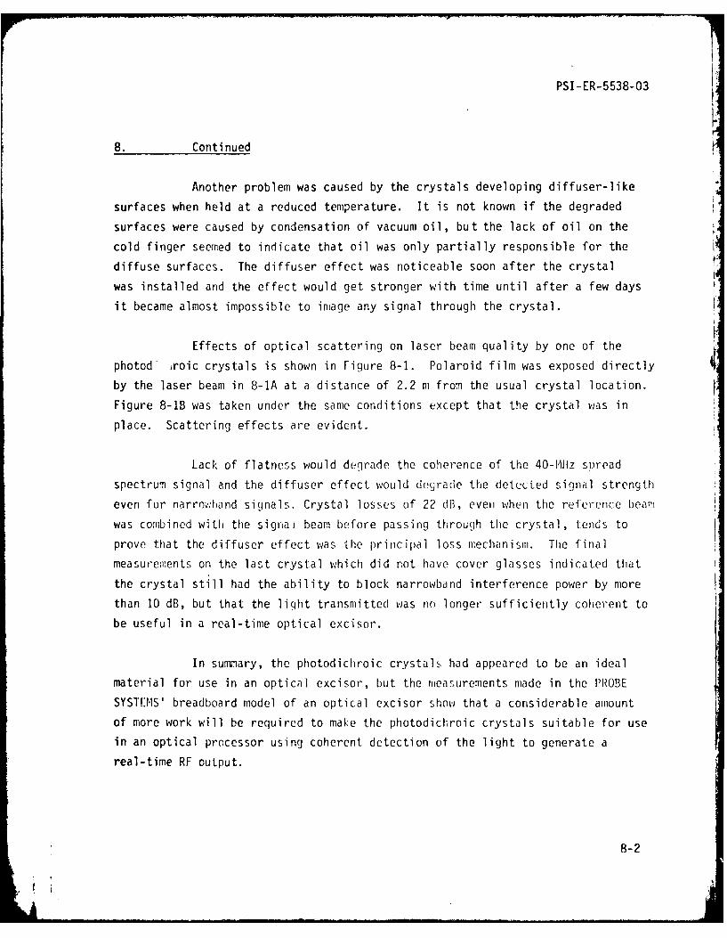
PSI-ER-5538-03
8. Continued
Another problem was caused by the crystals developing diffuser-like
surfaces when held at a reduced temperature. It is not known if the degraded
surfaces were caused by condensation of vacuum oil, but the lack of oil on the
cold finger seemed to indicate that oil was only partially responsible for the
diffuse surfaces. The diffuser effect was noticeable soon after the crystal
was installed and the effect would get stronger with time until after a few days
it became almost impossible to image any signal through the crystal.
Effects of optical scattering on laser beam quality by one of the
photod roic crystals is shown in Figure 8-1. Polaroid film was exposed directly
by the laser beam in 8-IA at a distance of 2.2 m from the usual crystal location.
Figure 8-1B was taken under the same conditions except that the crystal was in
place. Scattering effects are evident.
Lack of flatness would degrade the coherence of the 40-MHz spread
spectrum signal and the diffuser effect would degrade the detected signal strength
even for narro..:hand signals. Crystal losses of 22 dB, even when the reference beamwas combined with the signal beam before passing through the crystal, tends to
prove that the diffuser effect was the principal loss mechanism. The final
measurements on the last crystal which did not have cover glasses indicated that
the crystal still had the ability to block narrowband interference power by more
than 10 dB, but that the light transmitted was no longer sufficiently coherent to
be useful in a real-time optical excisor.
In summary, the photodichroic crystals had appeared to be an ideal
material for use in an optical excisor, but the measurements made in the PROBE
SYSTEMS' breadboard model of an optical excisor show that a considerable amountof more work will be required to make the photodichroic crystals suitable for use
in an optical processor using coherent detection of the light to generate a
real-time RF output.
8-2 ilA


PSI-ER-5538-03
SECTION 9
PHOTOCHROMIC GLASSES
Photochromic glasses were considered for use as optical clippers in
the excisor. When activated, usually by long-wave UV or short-wave visible light,
these glasses exhibit increased absorption across the visible spectrum. This
change in transmission characteristics results from photo-ionization and re-
combination of dopant ions and is a reversable process. Today, photochromic
glass is most commonly used in self-darkening sunglasses.
In several respects, photochromic glass is an optimal material for
use as a clipper -- long life, totally self-contained, no supporting electronics,
etc. Its disadvantages are limited dynamic range and slow response time. To
quantify the dynamic ranqe and response time, PROBE evaluated a glass -- Corning
Code 8111, "Photogrey Extra" -- in the lab. The sample was a plano-plano opthalmic
lens blank.
Figure 9-1 shows the optical setup used to evaluate the sample. An
argq laser operating at a wavelen th of 488.0 nm was used to activate the sam,,iple
and the trat,,::1ission was monitored with a laser power meter. An aperture, 600 1:m
in diameter, limited the area of exposure and gave a spot of uniform illumination.
This resulted in an incident optical power density of 71 mW/cm 2 on the glass
sample.
Optical power was recorded as a function of time, providing the dataplotted in Figure 9-2. In the response curve, we see a 3-dB change in attenuation
2in the first minute of exposure, which is approximately 4 J/cm . After 40 min-utes the attenuation reached 5.5 dB.
The optical quality of the photochromic glass was outstanding, and
therefore only the contrast and the relatively slow response time limit the
utility of photochromic glasses as optical clippers. Recent advances in new
photochromic glass may provide additional contrast and hence a deeper excision
9-1

PSI -ER-5538-03
LAj
C)0-
'-4
C) Cr)
V)
CD
C) c)l
ac
CL-
I-
F--

PSI-ER-5538-03
Cl) E
<-
-0 :c CS0 E )< LO
C) L) 0 -D(tl " co 00
C-) c 0 z C'
C) S-
=: o 0 e< <
o~ ~ C)
0) L-), r C)
C:>
CLjJ
co-
V))
UL
CD C
u
0 0D
6D CD
(UP) ssol NoIIuJstiI
9-3
PSI-ER-5538-03
K
9. Continued
notch, and they may also have a shorter response time. Until new glasses are
released, an optical excisor using photochromic glass will be useful primarily
for those applications where the interference levels only need to be reduced
less than 10 dB and where the frequency of each interference signal is only
slowly changing.
9-4

PSI-ER-5538-03
SECTION 10
OPTICAL CLIPPER CONCLUSIONS
The work reported here evaluated optical clipper materials that
have the potential to minimize the effects of narrowband RF interference when
used in a unique optical processor. The most successful results were obtained
with the PROM, an optically addressed optical memory. In the optical excisor
the PROM was able to attenuate the interference by nearly three orders of
magnitude. Another material evaluated was photodichroic crystals, but the
optical quality and scattering significantly reduced the utility of this type
of optical clipper. A photochromic glass was found to provide only 5 dB of
attenuation, but it was by far the easiest optical clipper to use.
Further development of optical clippers is recommended because the
laboratory results clearly demonstrate the ability of an optical excisor to
provide orders of magnitude improvements in broadband RF receiver performance.
However, optical clipper improvements are needed before a practical optical
excisor can be developed using an optical clipper. At this time, a more
practical approach is to replace the optical clipper with the electronic clipper
described in PROBE SYSTES' Report No. PSI-ER-5533-02.
10-1