Protection of MV Converters in the Grid: The Case of MV/LV ... · Protection of MV Converters in...
17
© 2017 IEEE IEEE Journal of Emerging and Selected Topics in Power Electronics, Vol. 5, No. 1, pp. 393-408, March 2017 Protection of MV Converters in the Grid: The Case of MV/LV Solid-State Transformers T. Guillod, F. Krismer, J. W. Kolar This material is published in order to provide access to research results of the Power Electronic Systems Laboratory / D-ITET / ETH Zurich. Internal or personal use of this material is permitted. However, permission to reprint/republish this material for advertising or promotional purposes or for creating new collective works for resale or redistribution must be obtained from the copyright holder. By choosing to view this document, you agree to all provisions of the copyright laws protecting it.
Transcript of Protection of MV Converters in the Grid: The Case of MV/LV ... · Protection of MV Converters in...

© 2017 IEEE
IEEE Journal of Emerging and Selected Topics in Power Electronics, Vol. 5, No. 1, pp. 393-408, March 2017
Protection of MV Converters in the Grid: The Case of MV/LV Solid-State Transformers
T. Guillod,F. Krismer,J. W. Kolar
This material is published in order to provide access to research results of the Power Electronic Systems Laboratory / D-ITET / ETH Zurich. Internal or personal use of this material is permitted. However, permission to reprint/republish this material for advertising or promotional purposes or for creating new collective works for resale or redistribution must be obtained from the copyright holder. By choosing to view this document, you agree to all provisions of the copyright laws protecting it.
IEEE JOURNAL OF EMERGING AND SELECTED TOPICS IN POWER ELECTRONICS, VOL. 5, NO. 1, MARCH 2017 393
Protection of MV Converters in the Grid:The Case of MV/LV Solid-State Transformers
Thomas Guillod, Student Member, IEEE, Florian Krismer, Member, IEEE, and Johann W. Kolar, Fellow, IEEE
Abstract— Solid-state transformers (SSTs) are a promisingtechnology as they provide new functionalities and servicesenabling future smart grids. An SST establishes the interfacebetween an MV ac grid and an LV (ac or dc) grid or load. TheSST must provide high reliability even in the event of certain gridfaults, where the SST is subject to exceptional electrical stresses.In addition, the MV and LV grids are exposed to failures ofthe SSTs. Spurred by such challenging requirements, this paperdefines the different relevant stresses, identifies the correspondingprotection needs, and proposes adequate protection circuitriesand devices. The protection mechanisms that are currently usedfor low-frequency transformers are analyzed and an adaptedversion is proposed for SSTs. MV short circuits and overvoltagesare identified as the most critical situations and are analyzed indetail. From the presented in-depth investigation, guidelines areextracted for designing robust SSTs and are applied to a 1 MVA,10 kV SST.
Index Terms— Power distribution faults, power electronics,power transformers, power-electronic transformers, solid-statetransformers (SSTs), substation protection, surge protection.
I. INTRODUCTION
CURRENTLY, interfacing between the different voltagelevels in the grid is done with low-frequency trans-
formers (LFTs). The need to integrate renewable energysources into LV ac or dc grids and the progress of thesemiconductor technology has led to the idea of solid-statetransformers (SSTs) where the power conversion is realizedwith a medium-frequency link [1]–[3]. SSTs are typicallyaimed to interface the MV ac grid (6–36 kV) with LV ac or dcgrids (48–400 V). SSTs have been proved to achieve a highefficiency conversion from ac to dc [4] and allow for powerflow control, active filtering, reactive power compensation,energy storage integration, and so on [3], [5]. In order touse these new features, different applications that have beenproposed and examined for SSTs are as follows.
1) SSTs used as distribution transformers (as a replacementfor an LFT) in a traditional distribution grid. In this case,the power flow is mainly directed from MV to LV andno monitoring or control of the loads is possible [4].
Manuscript received May 17, 2016; revised August 28, 2016; acceptedOctober 8, 2016. Date of publication October 13, 2016; date of currentversion January 31, 2017. This work is part of the Swiss CompetenceCenters for Energy Research (SCCER) initiative which is supported by theSwiss Commission for Technology and Innovation (CTI). Recommended forpublication by Associate Editor X. Ruan.
The authors are with the Power Electronic Systems Laboratory, SwissFederal Institute of Technology Zurich, 8092 Zurich, Switzerland.
Color versions of one or more of the figures in this paper are availableonline at http://ieeexplore.ieee.org.
Digital Object Identifier 10.1109/JESTPE.2016.2617620
2) SSTs forming the interface between the MV grid andsmart microgrids with renewable energy production andcontrol capabilities [3].
3) An SST employed to directly connect renewable energyplants (for example, PV plants) to the MV ac grid [3].
4) Industrial grids where SSTs could be used as unidi-rectional power supplies connected to the MV grid(datacenters, power-to-gas systems, etc.) [6].
5) SSTs used as a part of a locomotive power supply chainin order to replace LFTs [7], [8]. In this case, the SSTdoes not form the interface with a distribution grid.Therefore, this application is not considered further inthis paper.
All these applications require the SST to be integrated intothe grid. The SST, therefore, is subject to perturbations thatoriginate from the grid or the loads. The control of SSTs in thegrid has already been examined [3], [9] while the protection ofSSTs in the grid has so far not been covered in the literatureand remains a widely open topic [10]–[12]. From the abovelist of possible applications of SSTs, the first item, i.e., theusage of SSTs in a traditional three-phase distribution grid,leads to the largest stresses due to the lack of monitoring andcontrol capabilities of the surrounding system. For this reason,this application will be further considered. Yet, the presentedresults can be easily adapted to the alternative applications.
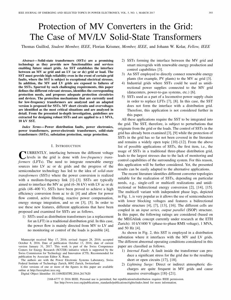
The recent literature identifies different converter topologiessuitable for the realization of SSTs, depending on particularneeds, e.g., single-cell or multicell realizations and unidi-rectional or bidirectional energy conversion [2], [14], [15].The multicell variant with independent phase legs, depictedin Fig. 1, is very popular as it allows the use of semiconductorswith lower blocking voltages and features a bidirectionalmodular structure [4], [7], [13], [16]. The different cells arecoupled in an input series, output parallel (ISOP) structure.In this paper, the following ratings are considered (based onthe MEGAlink concept currently under research at the ETHZurich): 10 kV/400 V (phase-to-phase RMS voltage), 1 MVA,and 50 Hz [4].
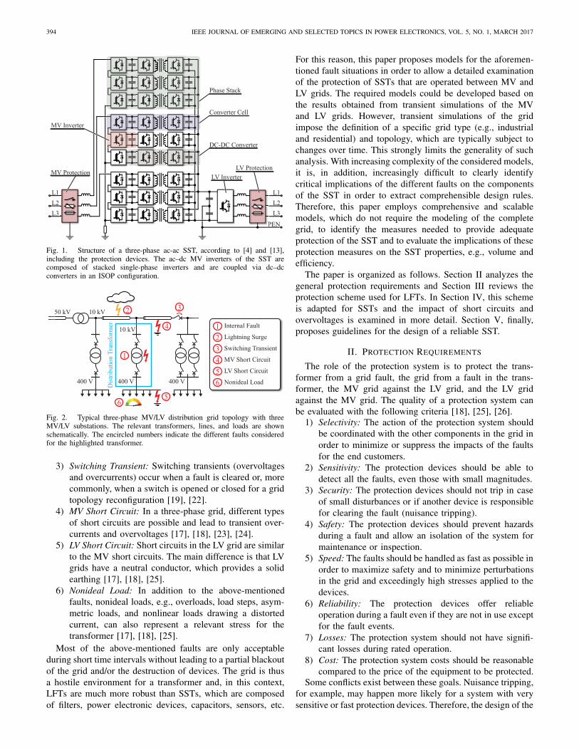
As shown in Fig. 2, this SST is employed in a distributionsubstation where it interfaces with the MV and LV grids.The different abnormal operating conditions considered in thispaper are classified as follows.
1) Internal Fault: A fault inside the transformer can pro-duce a significant stress for the grid due to the resultingshort or open circuits [17], [18].
2) Lightning Surge: Direct or indirect atmospheric dis-charges are quite frequent in MV grids and causemassive overvoltages [18]–[21].
2168-6777 © 2016 IEEE. Personal use is permitted, but republication/redistribution requires IEEE permission.See http://www.ieee.org/publications_standards/publications/rights/index.html for more information.
394 IEEE JOURNAL OF EMERGING AND SELECTED TOPICS IN POWER ELECTRONICS, VOL. 5, NO. 1, MARCH 2017
Fig. 1. Structure of a three-phase ac-ac SST, according to [4] and [13],including the protection devices. The ac–dc MV inverters of the SST arecomposed of stacked single-phase inverters and are coupled via dc–dcconverters in an ISOP configuration.
Fig. 2. Typical three-phase MV/LV distribution grid topology with threeMV/LV substations. The relevant transformers, lines, and loads are shownschematically. The encircled numbers indicate the different faults consideredfor the highlighted transformer.
3) Switching Transient: Switching transients (overvoltagesand overcurrents) occur when a fault is cleared or, morecommonly, when a switch is opened or closed for a gridtopology reconfiguration [19], [22].
4) MV Short Circuit: In a three-phase grid, different typesof short circuits are possible and lead to transient over-currents and overvoltages [17], [18], [23], [24].
5) LV Short Circuit: Short circuits in the LV grid are similarto the MV short circuits. The main difference is that LVgrids have a neutral conductor, which provides a solidearthing [17], [18], [25].
6) Nonideal Load: In addition to the above-mentionedfaults, nonideal loads, e.g., overloads, load steps, asym-metric loads, and nonlinear loads drawing a distortedcurrent, can also represent a relevant stress for thetransformer [17], [18], [25].
Most of the above-mentioned faults are only acceptableduring short time intervals without leading to a partial blackoutof the grid and/or the destruction of devices. The grid is thusa hostile environment for a transformer and, in this context,LFTs are much more robust than SSTs, which are composedof filters, power electronic devices, capacitors, sensors, etc.
For this reason, this paper proposes models for the aforemen-tioned fault situations in order to allow a detailed examinationof the protection of SSTs that are operated between MV andLV grids. The required models could be developed based onthe results obtained from transient simulations of the MVand LV grids. However, transient simulations of the gridimpose the definition of a specific grid type (e.g., industrialand residential) and topology, which are typically subject tochanges over time. This strongly limits the generality of suchanalysis. With increasing complexity of the considered models,it is, in addition, increasingly difficult to clearly identifycritical implications of the different faults on the componentsof the SST in order to extract comprehensible design rules.Therefore, this paper employs comprehensive and scalablemodels, which do not require the modeling of the completegrid, to identify the measures needed to provide adequateprotection of the SST and to evaluate the implications of theseprotection measures on the SST properties, e.g., volume andefficiency.
The paper is organized as follows. Section II analyzes thegeneral protection requirements and Section III reviews theprotection scheme used for LFTs. In Section IV, this schemeis adapted for SSTs and the impact of short circuits andovervoltages is examined in more detail. Section V, finally,proposes guidelines for the design of a reliable SST.
II. PROTECTION REQUIREMENTS
The role of the protection system is to protect the trans-former from a grid fault, the grid from a fault in the trans-former, the MV grid against the LV grid, and the LV gridagainst the MV grid. The quality of a protection system canbe evaluated with the following criteria [18], [25], [26].
1) Selectivity: The action of the protection system shouldbe coordinated with the other components in the grid inorder to minimize or suppress the impacts of the faultsfor the end customers.
2) Sensitivity: The protection devices should be able todetect all the faults, even those with small magnitudes.
3) Security: The protection devices should not trip in caseof small disturbances or if another device is responsiblefor clearing the fault (nuisance tripping).
4) Safety: The protection devices should prevent hazardsduring a fault and allow an isolation of the system formaintenance or inspection.
5) Speed: The faults should be handled as fast as possible inorder to maximize safety and to minimize perturbationsin the grid and exceedingly high stresses applied to thedevices.
6) Reliability: The protection devices offer reliableoperation during a fault even if they are not in use exceptfor the fault events.
7) Losses: The protection system should not have signifi-cant losses during rated operation.
8) Cost: The protection system costs should be reasonablecompared to the price of the equipment to be protected.
Some conflicts exist between these goals. Nuisance tripping,for example, may happen more likely for a system with verysensitive or fast protection devices. Therefore, the design of the

GUILLOD et al.: PROTECTION OF MV CONVERTERS IN THE GRID 395
TABLE I
DIFFERENT SHORT CIRCUIT TYPES IN AN MV OR LV GRID [17], [27]
Fig. 3. Qualitative time–current characteristics (selectivity) of the typicalprotection devices placed near a transformer (MV fuses, LV fuses, andLV breakers) [25], [26].
protection scheme is a tradeoff between the protection of thetransformer and the reliability of the grid. Now, these generalprinciples will be applied to the different faults involving atransformer (see Fig. 2).
A. Short Circuits
A short circuit can be caused by an insulation failure,a flashover, an incorrect configuration of the grid topology, etc.Short circuits can be classified as follows: faults produced byan internal failure, faults located upstream, and faults locateddownstream.
Table I defines different types of short circuits and thecorresponding abbreviations, for both the MV and the LVside [17], [27], [28]. These faults can be divided into severalcategories: symmetric faults (3p), asymmetric faults withoutearth connection (2p), and asymmetric faults with earth con-nection (1pg, 2pg). The magnitudes of the overcurrents dependon the impedances of the grid components and on the type offault. As most short circuits are not self-extinguishing, theprotection devices must be able to interrupt the short-circuitcurrents in the case of a grid fault or to isolate the transformerafter an internal fault.
The most important concept for achieving a reliableshort circuit protection is the selectivity as it minimizesor suppresses the impacts of the faults for the end cus-tomers [25], [26]. This is achieved by selecting more sensitiveand faster downstream (toward LV, low power) protectiondevices. Fig. 3 schematically depicts typical time–currentcharacteristics of the overcurrent protection devices.
The current selectivity defines lower fault current limits nearthe end customers. The time selectivity adds delays for trippingthe protection in the direction of the MV/HV grids. Thesetime delays also help in the identification of a fault and, thus,
Fig. 4. Time–voltage characteristics of overvoltages in the MV grid(normalized with respect to the nominal phase-to-earth peak voltage). Thetimes tr and tf represent the rise time and the total duration of the surgeswhere some overlaps exist between the different overvoltage types. The givenlevels are only typical values that can vary between grids [19], [30], [31].
to avoid nuisance tripping. Finally the logic selectivity is basedon communication between the different protection devicesand is used to localize the fault [17], [25].
One implication of the selectivity is that the MV/LV trans-former should be able to carry an important fault current fora defined time. In the case of an LV short circuit, the MV/LVtransformer should be the last device to trip in the whole LVgrid. The current threshold is typically increased by 25% perprotection stage and the time delay can be more than 1 s forshort circuit currents at the transformer [17], [18], [29].
B. Overvoltages
Overvoltages have a critical impact on the insulationcoordination of the transformer [30]. Fig. 4 depicts typicaltime–voltage characteristics of different overvoltage conditionsin the MV grid [19], [31]. A similar diagram also exists forLV grids [21], [25]. Due to the impedances of the cables andthe different components, overvoltage transients also producetemporary overcurrents.
Very fast front surges are mostly created by arcing,extinguish, and restrike processes in switchgears and carryrelatively low energies. Lightning surges generate the largestovervoltages in the grid. MV overhead lines and renewableenergy plants may be subject to direct lightning strikes.Indirect strikes or transmitted surges (from higher voltage levelgrids) may also occur in grids with underground cables. Theenormous current injected by a lightning surge (typically inthe range of several 10 kA) produces a massive overvoltage(up to several MVs) during a short time interval [31]–[35].
Switching transients result from the energization/de-energization processes (short circuit interruption,transformer turn-on inrush current, load connection, etc.).The inductances and capacitances present in the distributiongrid abet ringing, which typically appears in the kHz rangeand fades away after some milliseconds [22], [31], [32].
Temporary overvoltages mostly occur during earth faults(see Table I). Depending on the earthing policy of the system),the phase-to-phase voltage can appear in place of the phasevoltage during an earth fault [20], [28]. Due to the timeselectivity requirement (see Section II-A), these types of short

396 IEEE JOURNAL OF EMERGING AND SELECTED TOPICS IN POWER ELECTRONICS, VOL. 5, NO. 1, MARCH 2017
Fig. 5. Star–star distribution LFT with typical protection devices. The MVside of the LFT is earthed with a resistor and the LV side has a solid earthconnection (with a TN-C earthing concept) [17], [18], [25].
circuits can be present for hundreds of milliseconds. Thepermanent allowed overvoltage (voltage control tolerance) fora typical distribution grid is 10%–20% [20], [36].
III. PROTECTION OF LFTS
With known policies related to the dimensioning of theprotection devices and the discussion of critical overcurrentand overvoltage situations in Section II, the state-of-the-artprotection scheme for an MV/LV LFT is analyzed in thissection.
A. LFT Capabilities and Protection Scheme
Relevant IEC/IEEE norms require the LFT itself (withoutexternal protection devices) to be robust with respect toovervoltages and overcurrents. For a 1 MVA LFT connectedto the 10 kV grid (phase-to-phase RMS nominal systemvoltage [36]), the following limits apply.
1) Highest Voltage for Equipment: 12 kV maximumoperating voltage, it excludes transient overvolt-ages [31], [36].
2) Short Duration Power Frequency Voltage: 20 kV dielec-tric withstand value for 1 min [31].
3) Lightning Impulse Voltage: 60–75 kV dielectricwithstand against lightning surges (ca. 50 µs,MV side) [31], [32].
4) Short Circuit Impedance: 5.0% minimum impedance inorder to limit the short circuit current flowing in thephase conductors of the LFT [31].
5) Overload Capabilities: This is dependent on the LFTtype (cooling, insulation, etc.) but the following estima-tions can be taken for oil insulated LFTs: 25× the ratedcurrent for 2 s, 11× for 10 s and 3× for 300 s [37].
A comparison of these ratings with the requirements definedin Section II indicates that additional protection devicesare required. A simplified scheme of a typical MV/LVLFT is shown in Fig. 5 [17], [18], [25] and is detailedin Sections III-B–III-D.
B. Short Circuits, Overload, and Isolation
The LFT itself is not able to interrupt a short circuit.Therefore external protection devices are required in order toclear the faults. In the protection scheme presented in Fig. 5,
different devices are capable of interrupting the line currents(MV and LV sides) as follows [18], [22], [25].
1) Disconnector: Disconnectors are used to disconnect theLFT from the MV and LV grids in order to allow properearthing for voltage free maintenance. These devices canonly switch currents that are considerably lower than thenominal current.
2) Fuse: Fuses exist for the MV and LV sides and provideirreversible overcurrent protection. MV fuses are notable to break currents below the minimum breaking cur-rent, which is larger than the nominal current. Therefore,typical MV fuses provide only protection against shortcircuits and not against overloads, while LV fuses canalso provide protection against overload (see Fig. 3).
3) Breaker: Breakers are able to break a short circuitcurrent. The total breaking time of a breaker is typically50–100 ms (without additional delays required by thetime selectivity). For ac systems, the break event occursat or close to the zero crossing of the respective phasecurrents. This device is expensive compared to a loadswitch or a fuse.
4) Load Switch: A load switch is only able to breaknominal and overload currents but not short circuitcurrents. In Fig. 5, load switches could be used in placeof breakers for basic substations, which, however, is lessflexible, as the fuse is responsible for clearing shortcircuit currents [17].
For a standard distribution substation, breakers are onlypresent at the LV side and are responsible for LV short circuitand overload protections (see Fig. 5) [25], [29]. As breakersare complex devices, LV fuses are also present in order toimprove the reliability of the system (or to interrupt faultcurrents exceeding the capabilities of the breakers) [25], [29].
The LV breakers cannot clear all short circuits, i.e., inthe case of an internal failure of the transformer. Therefore,MV fuses are also required to disconnect the transformer fromthe MV grid (see Fig. 5). Complex substations may employadditional breakers or load switches at the MV side [17].
C. Overvoltages
For the overvoltage protection, the insulation levels definedin Section III-A (short duration power frequency voltageand lightning impulse voltage) are sufficient for handlingswitching overvoltages and power frequency overvoltages.The surge arresters depicted in Fig. 5 limit the maximumphase-to-earth voltages during lightning surges. State-of-the-art transformers use metal-oxide surge arresters on the MV andLV sides [18], [20].
A metal-oxide arrester features a highly nonlinear andvoltage-dependent resistance, which enables it to clamp theapplied voltage to a certain (device-specific) clamping voltage,which is typically between two and three times the continuousoperating voltage [20]. The transformer can withstand thisincreased voltage, as the resulting clamping voltage is still lessthan the lightning impulse voltage the transformer is designedfor. As the thermal rating of a surge arrester only allows shortpulses (lightning, switching surges), the device should not

GUILLOD et al.: PROTECTION OF MV CONVERTERS IN THE GRID 397
TABLE II
ADVANTAGES AND LIMITATIONS OF THE DIFFERENT EARTHINGCONCEPTS USED FOR MV DISTRIBUTION GRIDS [20], [38]
conduct in the event of temporary overvoltages (see Fig. 4).For this reason and depending on the earthing concept, eachsurge arrester may need to be dimensioned for the phase-to-phase instead of the phase-to-earth voltage [20], [28].
D. Earthing
The earthing of the LFT is an important aspect: accordingto Fig. 5, the earthing of star-points is different for theLFT’s LV and MV sides. This has a decisive impact on theshort circuit currents and voltages. The LV side of an LFThas a solid earth connection for safety reasons and in orderto provide a protective earth neutral conductor (PEN) [26],[38]. This implies that only the impedances of lines andtransformers limit the short circuit currents on the LV side.On the MV side, only three conductors are distributed,which enables the realization of different earthing conceptsas follows [23], [25], [38].
1) Solid Earthing (R0 ≈ 0): Solid earthing is usually notused in the case of a three-phase distribution system.Transient overvoltages are limited, however, short circuitcurrents are very high during a 1pg fault (see Table I).Therefore, the usage of solid earthing is limited to gridswith reduced short circuit power.
2) Unearthed (R0 → ∞): The star-point is only connectedto the earth through parasitic capacitances or no star-point is present (delta winding). The advantages ofthis earthing concept are the limited earth short circuitcurrents and the possibility to operate the grid witha 1pg fault (see Table I). The main drawbacks arethe difficulty to detect earth faults without additionalmonitoring and that overvoltages appear at the star-pointduring asymmetric faults.
3) Resistance Earthing (R0): A resistor is placed betweenthe star-point and the earth for limiting the short circuitcurrents. This variant is a compromise between limitingthe short circuit currents and the overvoltages. Theresistance also damps oscillations during fault transients.For these reasons, this is the typical earthing method forMV grids.
Table II summarizes the advantages and the limitations ofdifferent earthing concepts where the given values can varybetween grids (voltage level, short circuit power, etc.) andare here given only as typical examples. The fault currentis expressed by the factor kI , which is defined as the ratio
between the single phase-to-earth (1pg) fault current and thethree-phase symmetrical 3p fault current (3p), which is oftentaken as a reference value [17], [24], [28]. The factor kI ,together with the overcurrent capability of the LFT, determinesthe maximum acceptable duration of a 1pg fault.
During a 1pg fault, the star-point of the SST is shiftedwith respect to earth (see [10]). As a consequence, one ormore phase-to-earth voltages exceed their nominal values. Thiseffect is quantified by the earth fault factor kV , which is theratio of the phase-to-earth voltages during a 1pg fault withrespect to nominal conditions. Even with a solid connectionto earth, the earth fault factor is greater than one due to theearth resistance.
Therefore, the choice of the MV earthing concept is atradeoff between short circuit currents and overvoltages. In anycase, the earthing should be matched between the differentdevices composing the grid [10], [24]. Therefore, earthing isa grid policy which can vary between countries [38].
IV. PROTECTION OF SSTs
The disturbances occurring in grids and the protectionscheme of an LFT have been examined in Sections II and III,respectively. With this, a protection scheme is derived forSSTs and the impact of LV and MV faults (short circuits andovervoltages) is analyzed in this section.
A. SST Capabilities
As shown in Fig. 1, the SST is a complex device and,as a consequence, a multitude of different failure modesare possible, e.g., semiconductor failures, thermomechanicalfailures, control errors, or insulation breakdowns (particularlycritical for the MV side converter [7], [16]). Moreover, SSTshave limited current and voltage overload capabilities, wherethe employed semiconductors are identified to mainly restrictthe SST’s overload capabilities. However, the high complexityof SSTs can be compensated for with redundancy, as oftendone for multicell SST topologies (see Fig. 1), in order toincrease the mean time between failures [7], [13].
With regard to overcurrent capabilities, thermal time con-stants in the range of several seconds apply for the packagesof power semiconductor switches and milliseconds for thechips, which dramatically limit the allowable durations ofovercurrents. For an SST, the typical maximum allowableovercurrent ratios are in the range of 1.5× for some minutesand 4× for some milliseconds [4], [12], [39], [40]. In addition,the input filter inductor saturates at exceedingly high currents,which also limits the maximal allowed current of the SST.
Further particular challenges include robustness againstovervoltages, as semiconductors may not withstand voltagesthat exceed their maximum blocking voltage capability. Due tocosmic ray-induced failures and transient overvoltages duringswitching, the voltage utilization of power devices is usu-ally between 40% and 70% [4], [41], leaving a margin forhandling faults with short durations of up to some hundredmilliseconds. Moreover, the passive components (input filter,dc-link capacitor), where increased breakdown voltages applyfor pulses with short durations, provide a smoothing effect for

398 IEEE JOURNAL OF EMERGING AND SELECTED TOPICS IN POWER ELECTRONICS, VOL. 5, NO. 1, MARCH 2017
Fig. 6. Proposed protection scheme for an SST based on classical protectiondevices. Earthing of the MV side is realized with a resistor and the LV sideis solidly earthed.
the surges [22], [42]. As a consequence, possible worst casecharacteristics of transient overvoltages are not only linked to aselection of appropriate protection devices and semiconductorblocking voltages, but also to a suitable design of the inputfilter and the dc-link capacitor.
The main feature of an SST is its ability to control phasecurrents and voltages. The SST is also capable to operateunder nonideal operating conditions, e.g., in the presence ofa voltage dip, asymmetrical loads, nonlinear loads, and soon [3], [43]. The dc-links of the SST offer decoupling betweenthe MV and LV grids. This means that disturbances are nottransmitted from one grid to another grid [5], [39], [44].Moreover, the SST features highly dynamic current controlproperties (LV and MV sides), allowing the interruption ofphase currents in some milliseconds [3], [44], [45]. Thisimplies that an SST can be shut down very quickly and withoutopening a mechanical breaker. Finally, SSTs feature advancedmonitoring capabilities. The current and voltage measurementsthat are required for the control of the SST can be used foridentifying faults and overload situations [3], [44].
B. Proposed Protection Scheme
As SSTs are considerably more sensitive to overcurrentsand overvoltages than LFTs, external protection devices arerequired. In Fig. 6, an adapted version of the discussed LFTprotection scheme (see Fig. 5) is proposed for SSTs. Thefunctional principle of the proposed protection scheme isexplained based on the following listed events.
1) Overvoltage: Metal-oxide surge arresters are placed atthe MV and LV sides in order to clamp large overvolt-ages. As the overvoltage capabilities of SSTs are limited,surge arresters are also placed between the phases inorder to achieve better clamping [20].
2) Overcurrent: Fuse/breaker combinations are used on theMV and LV sides for interrupting the phase currents.MV breakers are required, due to the SST’s limited over-current capability and for disconnecting the SST after anMV short circuit or an internal failure [12], [17], [40].Fuses are also present as a last resort grid protection.Due to the current control capabilities of SSTs, shortcircuit current breaking is only required in the case ofan internal failure of the SST. The probability of aninternal failure is low and, in this case, a fast overcurrentprotection is no more required. This implies that the
breakers could be replaced by a less expensive fuse/loadswitch combinations.
3) Isolation: Disconnectors are present on both the sides inorder to allow for voltage free maintenance [17], [25].
4) Startup: The MV side inverters of an SST most com-monly act as diode rectifiers during the startup procedure(see Fig. 1), making precharging resistors and bypassload switches necessary in order to limit the inrushcurrents [7], [46]. Similar devices are required at theLV side for starting the SST from the LV grid.
As explained in Section III-D for LFTs, the LV siderequires a solid earthing and different choices are possiblefor the MV side. The multicell SST with separated phasestacks (see Fig. 1) features a star-point, allowing the earth-ing via a resistor R0 [20], [38]. This protection scheme isanalyzed in more detail in Sections IV-C–IV-F. Thereafter,in Section IV-G, an advanced protection scheme based onsolid-state devices is presented.
C. LV Faults
On the LV side, the expected overvoltages strongly dependon the loads (switching overvoltages) and on whether over-head lines are present (lightning surges). A large varietyof LV surge protection devices with low clamping volt-ages are readily available, e.g., surge arresters and breakoverdiodes [17], [21], [25]. Furthermore, protection conceptsalready detailed for solar inverters and grid connected rectifierscan be used [25], [47], [48]. For these reasons, the LVovervoltage protection is not further discussed in this paper.
The control capabilities of SSTs allow the compensationof nonideal loads in a wide range and an effective overloadprotection [3], [18], [43], [44]. In the case of LV short circuits,the presence of a neutral conductor allows a fast identificationof the fault (see Table II). The SST is able to interrupt thecurrent immediately, which, however, violates the selectivitypolicy discussed in Section II-A, because the downstreambreakers or fuses do not trip. In this case, all the LV loadswould experience a blackout. In order to avoid this situation,the SST needs to inject short circuit current in the LV griduntil the following occur [3], [44].
1) A downstream breaker or a fuse interrupts the fault.Afterward, the SST restores the voltage for the remain-ing loads.
2) The downstream breakers or fuses cannot interrupt thefault (for example, if the fault is located at the outputof the SST). After some seconds, the SST reduces thecurrent to zero and conducts a shutdown.
3) If neither the downstream breakers nor the SST are ableto interrupt the fault (failure of the LV side of the SST),then the LV breakers (see Fig. 6) will open in order tointerrupt the fault current supplied by the LV grid.
For these three cases, the short circuits are not transmittedto the MV grid as the SST decouples the MV and LV grids.Another important question is the required current that theSST should inject in order to trip the downstream protectiondevices, which is dependent on the power ratings of theLV downstream fuses. Tripping a 1 MVA LV side fuse of

GUILLOD et al.: PROTECTION OF MV CONVERTERS IN THE GRID 399
a 1 MVA SST, for example, requires 12 s at 5× the ratedcurrent while a 500 kVA fuse will still need 20 s at 2× therated current [49]. As stated in Section IV-A, a typical SSTcan deliver only up to 1.5× of the rated current which, thus,is insufficient for breaking the fuse of the SST or a largeload [18], [25]. Fulfilling this requirement would thereforerequire a substantial overrating of the LV inverter.
A possible alternative solution considers more sensitive LVbreakers [12], [18]. As the SST is able to limit the fault current,load switches can be used instead of breakers in the LV grid.In the case of a smart grid environment, the improved logicselectivity allows a rapid identification of the fault and theSST does not have to inject a large short circuit current [3],[9], [43]. In any case, the LV grid selectivity and the SSTovercurrent capability need to be matched.
D. MV Side Characteristic Properties
In order to extract figures of merit for SSTs with differentvoltage and power levels, all the characteristic electrical para-meters are scaled by means of a per-unit system. The followingscaling is defined:
vp =√
2√3
V , ip =√
2√3
S
V, Zb = V 2
S(1)
where vp is the peak phase-to-earth voltage, ip the peak phasecurrent, and Zb the phase impedance. These values are used toscale voltages, currents, and impedances, respectively. In (1),V is the rated phase-to-phase RMS voltage and S the ratedthree-phase power.
The short circuit ratio (SCR) is the ratio between thenominal phase current and the symmetric three-phase shortcircuit current (3p fault, see Table I) and can be expressed as(for LFT and SST) [17], [31]
SCR = ZSCR
Zb, ZSCR = ZSCRe j arctan(XR) = SCRZb (2)
where ZSCR is the short circuit impedance and XR the ratiobetween the reactance and the resistance. For an SST, theSCR characterizes the input filter impedance (see Fig. 1)where a purely inductive filter (without saturation and withoutcapacitors) is employed [4], [12].
The MV earthing resistor (for LFT and SST) is scaled withrespect to the base impedance of the system and forms theearthing impedance ratio (EIR)
EIR = R0
Zb. (3)
For the modeling of the ac–dc inverters, the energy storedin the dc-links and the maximum applied voltage at theac port are considered for basic fault considerations. Themodeling of the multilevel ac voltage is not required. Thisimplies that the multicell structure (see Fig. 1) can be reducedto an equivalent virtual single-cell structure with a dc-linkconsisting of the series connection of all MV dc-links ofthe corresponding phase [13]. With this transformation, theaforementioned properties remain unchanged. The dc-linkvoltage and capacitance of this virtual single-cell structure are
TABLE III
PARAMETERS USED FOR THE MV MODELS [4], [13]
Fig. 7. (a) Equivalent circuit of the LFT feeder where the possible gridshort circuits are highlighted. (b) MV equivalent circuit of the SST with theconsidered internal short circuit faults. The multicell structure is replaced bya virtual single cell per phase.
scaled and form the capacitor voltage ratio (CVR) and thecapacitor energy ratio (CER), respectively
CVR = VDC,0
vp, CER =
CDC V 2DC,0
2S/32 f
= CDCCVR2 Zb2 f (4)
where VDC,0 is the nominal dc-link voltage and f the gridfrequency. The CER is the ratio between the energy stored inthe dc-link capacitor and the energy consumed by one phaseduring a grid half-period.
The analysis assumes the MV side of the SST to be fedby a standard HV/MV LFT with the same power rating(50 Hz grid). The SST depicted in Fig. 1 is chosen [4] andTable III summarizes the parameters used for the correspond-ing MV models. The short circuit power of the feeder willincrease for an MV feeder with a larger power rating. However,the required short circuit impedance is larger for high powerLFTs such that the increase in the short circuit power islimited [31].
E. MV Short Circuits
1) Modeling: The presented short circuit analysis is basedon the model presented in Fig. 7. The length of the connectionbetween the LFT feeder and the SST is assumed to bezero (back-to-back connection), as this configuration leads to

400 IEEE JOURNAL OF EMERGING AND SELECTED TOPICS IN POWER ELECTRONICS, VOL. 5, NO. 1, MARCH 2017
Fig. 8. Converter fault currents (iin,SST) during internal SST faults. DifferentSST SCR values are considered with a solidly earthed and an unearthed MVfeeder. Currents (maximum over the three phases) are normalized to the phasepeak current ip [see (1)].
the largest fault current [24]. The resistance RF (earth faultresistance) is 0.1% of the base impedance Zb (low ohmicfault). This paper considers two possible cases for an SSTthat is subject to an MV short circuit.
1) SST Internal Fault: Due to an internal failure, the SSTcauses a short circuit after the filter inductor. In casethe switches are still operational, the MV ac–dc stagesshut down, i.e., opens all switches, but a current is stillpresent at the input (iin,SST �= 0 in Fig. 7).
2) Grid Short Circuit: A short circuit occurs between theMV feeder and the SST. The SST shuts down theMV ac–dc stages. After a short initial transient, the inputcurrent of the SST is zero (iin,SST = 0 in Fig. 7).
2) SST Internal Fault: Internal failures can be located afterthe filter, inside the ac–dc inverters, at the dc buses, etc.DC bus faults have already been examined in [12]. The higheststeady-state short circuit currents inside the SST occur duringa fault placed after the filter (see Fig. 7(b)), and therefore thiscase is further considered.
During an internal failure of the SST, the SST is notanymore able to interrupt the MV current and the MV breakerswill clear the fault. However, due to the reaction time of theMV breakers and due to selectivity, short circuit currents stillflow into the SST. In order to limit the short circuit currents,an SCR of at least 5.0% is required by the IEC norms [31].
Fig. 8 depicts the steady-state amplitudes of the fault cur-rents (iin,SST in Fig. 7) flowing into the SST owing to differentinternal failures. Different SST short circuit impedances andtwo differently earthed MV feeders are considered (EIRLFT).The earthing of the SST (EIRSST) has no impact on thecomputed currents as the fault occurs before the ac–dc invert-ers, which are turned off. For this reason, no current flowsthrough the star-point of the SST. A fault occurring inside theac–dc inverters (between the ac terminals) leads to smallerfault currents, due to the current limiting effect of EIRSST.This implies that the faults chosen in Fig. 8 are the worstcases.
The 3p fault produces the largest current, independent ofthe type of earthing. By contrast, the 1pg fault current is zeroin the case of an unearthed MV feeder (no current path exists).Globally, it can be seen that the value of the fault current canbe adjusted by a proper choice of the SCR of the SST (definedby the MV side filter inductor). The maximum fault current
(3p fault), can be easily computed as
iin,SST = ip
∣∣∣∣
1
SCRLFT + SCRSST
∣∣∣∣. (5)
A low-frequency current component appears during the initialfault transient (superimposed on the steady-state sinusoidalcurrent). This can lead to a peak current of up to twicethe steady-state value [17], [28], [31]. This low-frequencycomponent is damped by the earthing resistor and the XR ratioand converges (typically in less than 50 ms) toward the valuesshown in Fig. 8 [17], [27].
From the presented results, it can be seen that an SCR ofless than 10% will lead to very large fault currents, greaterthan 7 p.u., in the filter. A lower SCR value would lead toimportant fault currents in the grid and to hazardous currentsinside the SST [7]. Moreover, the filter impedance limits theinitial current during failures of the ac–dc inverters, whichprevents the instantaneous transfer of the energy stored in thedc-links into the grid. It can be further concluded that thefilter inductor needs to be capable of carrying the short circuitcurrent until a breaker clears the fault, which can take morethan a hundred milliseconds. Furthermore, a decrease in thefilter inductance at high currents due to saturation also needs tobe considered in the course of the design of the SST. However,this current is only flowing in the case of an internal failure ofthe SST and, thus, does not have an implication on the currentratings of the ac–dc inverters.
3) Grid Short Circuit: During an MV grid short circuit, theSST tries to actively control the fault current [5], [9], [11].However, this requires a fast identification of the fault in orderto react appropriately. Furthermore, the SST control strategyaims to avoid a mismatch between the MV and LV powerflows, which causes a rapid change in the dc-link voltages.If the SST is not able to control the current, the ac–dc inverters(and the dc–dc converters) initiate a shutdown. This last case isconsidered in this paper, as it has been identified to representthe worst case.
During a grid earth fault, the amplitudes of one or morephase-to-earth voltages at the input of the SST increase andmay, in the worst case, reach the amplitude of the phase-to-phase voltage (see Section III-D) [20], [24]. Depending onthe EIRLFT and EIRSST, this may lead to an increase in theac voltages applied to the SST’s input inverters, i.e., vAC,SSTin Fig. 7. If the instantaneous input voltages are greater thanthe dc-link voltages, an effective shutdown of the SST is notpossible as the shutdown ac–dc inverters act as diode rectifiers.Fig. 9 depicts the charging process of the MV dc-links duringa 1pg fault with a resistance earthing. The dc-link voltage ofthe faulted phase is not affected, while the voltage rises forthe remaining phases. In the presented simulation, the MVbreakers interrupt the increase of the dc-link voltages after80 ms [27], [29].
The applied steady-state overvoltage (vin,SST in Fig. 7) isshown in Fig. 10(a) for different earthing of the MV feederand fault types. The identified worst-case scenario is thesingle phase-to-earth fault (1pg) and the derivation of the
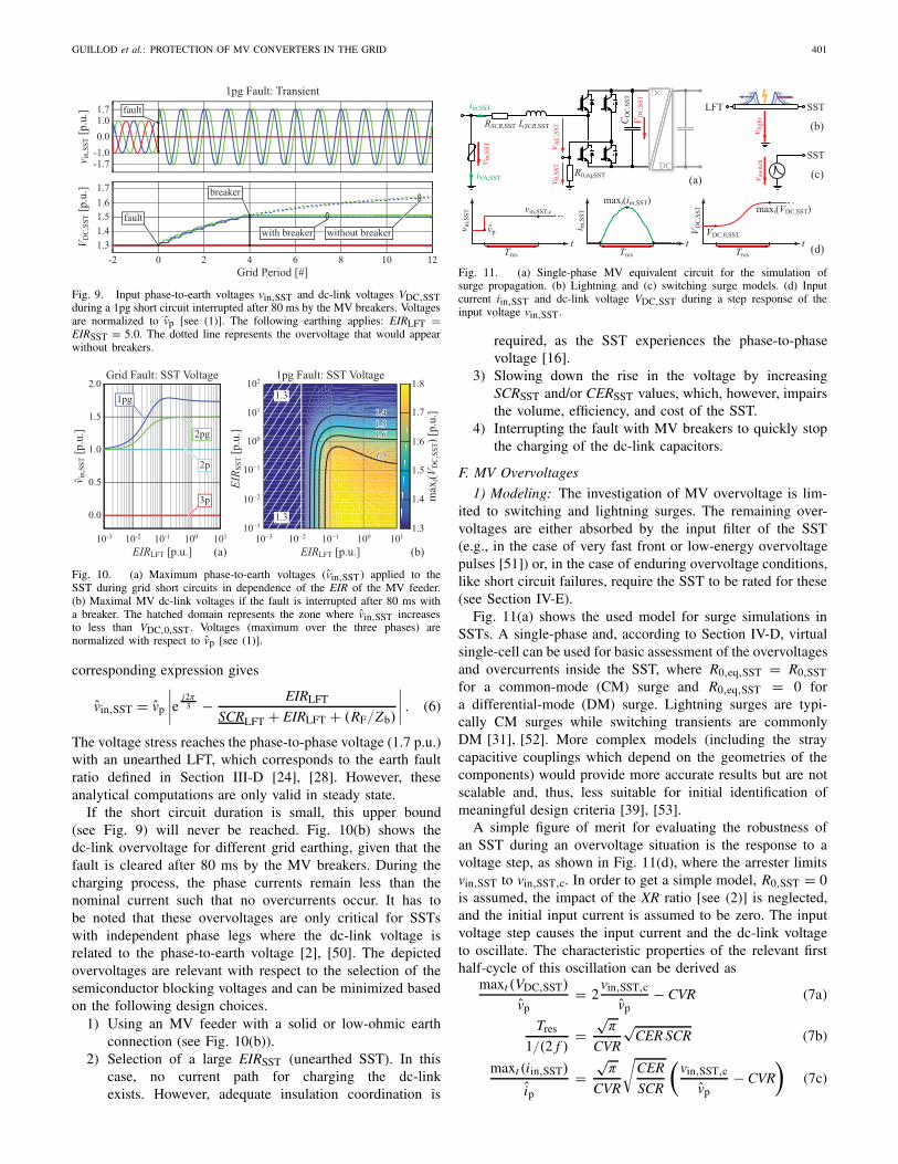
GUILLOD et al.: PROTECTION OF MV CONVERTERS IN THE GRID 401
Fig. 9. Input phase-to-earth voltages vin,SST and dc-link voltages VDC,SSTduring a 1pg short circuit interrupted after 80 ms by the MV breakers. Voltagesare normalized to vp [see (1)]. The following earthing applies: EIRLFT =EIRSST = 5.0. The dotted line represents the overvoltage that would appearwithout breakers.
Fig. 10. (a) Maximum phase-to-earth voltages (vin,SST) applied to theSST during grid short circuits in dependence of the EIR of the MV feeder.(b) Maximal MV dc-link voltages if the fault is interrupted after 80 ms witha breaker. The hatched domain represents the zone where vin,SST increasesto less than VDC,0,SST. Voltages (maximum over the three phases) arenormalized with respect to vp [see (1)].
corresponding expression gives
vin,SST = vp
∣∣∣∣e
j2π3 − EIRLFT
SCRLFT + EIRLFT + (RF/Zb)
∣∣∣∣. (6)
The voltage stress reaches the phase-to-phase voltage (1.7 p.u.)with an unearthed LFT, which corresponds to the earth faultratio defined in Section III-D [24], [28]. However, theseanalytical computations are only valid in steady state.
If the short circuit duration is small, this upper bound(see Fig. 9) will never be reached. Fig. 10(b) shows thedc-link overvoltage for different grid earthing, given that thefault is cleared after 80 ms by the MV breakers. During thecharging process, the phase currents remain less than thenominal current such that no overcurrents occur. It has tobe noted that these overvoltages are only critical for SSTswith independent phase legs where the dc-link voltage isrelated to the phase-to-earth voltage [2], [50]. The depictedovervoltages are relevant with respect to the selection of thesemiconductor blocking voltages and can be minimized basedon the following design choices.
1) Using an MV feeder with a solid or low-ohmic earthconnection (see Fig. 10(b)).
2) Selection of a large EIRSST (unearthed SST). In thiscase, no current path for charging the dc-linkexists. However, adequate insulation coordination is
Fig. 11. (a) Single-phase MV equivalent circuit for the simulation ofsurge propagation. (b) Lightning and (c) switching surge models. (d) Inputcurrent iin,SST and dc-link voltage VDC,SST during a step response of theinput voltage vin,SST.
required, as the SST experiences the phase-to-phasevoltage [16].
3) Slowing down the rise in the voltage by increasingSCRSST and/or CERSST values, which, however, impairsthe volume, efficiency, and cost of the SST.
4) Interrupting the fault with MV breakers to quickly stopthe charging of the dc-link capacitors.
F. MV Overvoltages
1) Modeling: The investigation of MV overvoltage is lim-ited to switching and lightning surges. The remaining over-voltages are either absorbed by the input filter of the SST(e.g., in the case of very fast front or low-energy overvoltagepulses [51]) or, in the case of enduring overvoltage conditions,like short circuit failures, require the SST to be rated for these(see Section IV-E).
Fig. 11(a) shows the used model for surge simulations inSSTs. A single-phase and, according to Section IV-D, virtualsingle-cell can be used for basic assessment of the overvoltagesand overcurrents inside the SST, where R0,eq,SST = R0,SSTfor a common-mode (CM) surge and R0,eq,SST = 0 fora differential-mode (DM) surge. Lightning surges are typi-cally CM surges while switching transients are commonlyDM [31], [52]. More complex models (including the straycapacitive couplings which depend on the geometries of thecomponents) would provide more accurate results but are notscalable and, thus, less suitable for initial identification ofmeaningful design criteria [39], [53].
A simple figure of merit for evaluating the robustness ofan SST during an overvoltage situation is the response to avoltage step, as shown in Fig. 11(d), where the arrester limitsvin,SST to vin,SST,c. In order to get a simple model, R0,SST = 0is assumed, the impact of the XR ratio [see (2)] is neglected,and the initial input current is assumed to be zero. The inputvoltage step causes the input current and the dc-link voltageto oscillate. The characteristic properties of the relevant firsthalf-cycle of this oscillation can be derived as
maxt (VDC,SST)
vp= 2
vin,SST,c
vp− CVR (7a)
Tres
1/(2 f )=
√π
CVR
√CER SCR (7b)
maxt (iin,SST)
ip=
√π
CVR
√
CER
SCR
(vin,SST,c
vp− CVR
)
(7c)
402 IEEE JOURNAL OF EMERGING AND SELECTED TOPICS IN POWER ELECTRONICS, VOL. 5, NO. 1, MARCH 2017
where Tres is the duration of the current half-cycle resonance(assuming a non-saturating filter inductor), which is also thetime where the maximum dc-link overvoltage is reached. Dueto resonance, the maximum dc-link voltage is larger than theclamping voltage of the MV side surge arrester. The durationTres is useful in order to assess the immunity of the SST againstshort duration overvoltages.
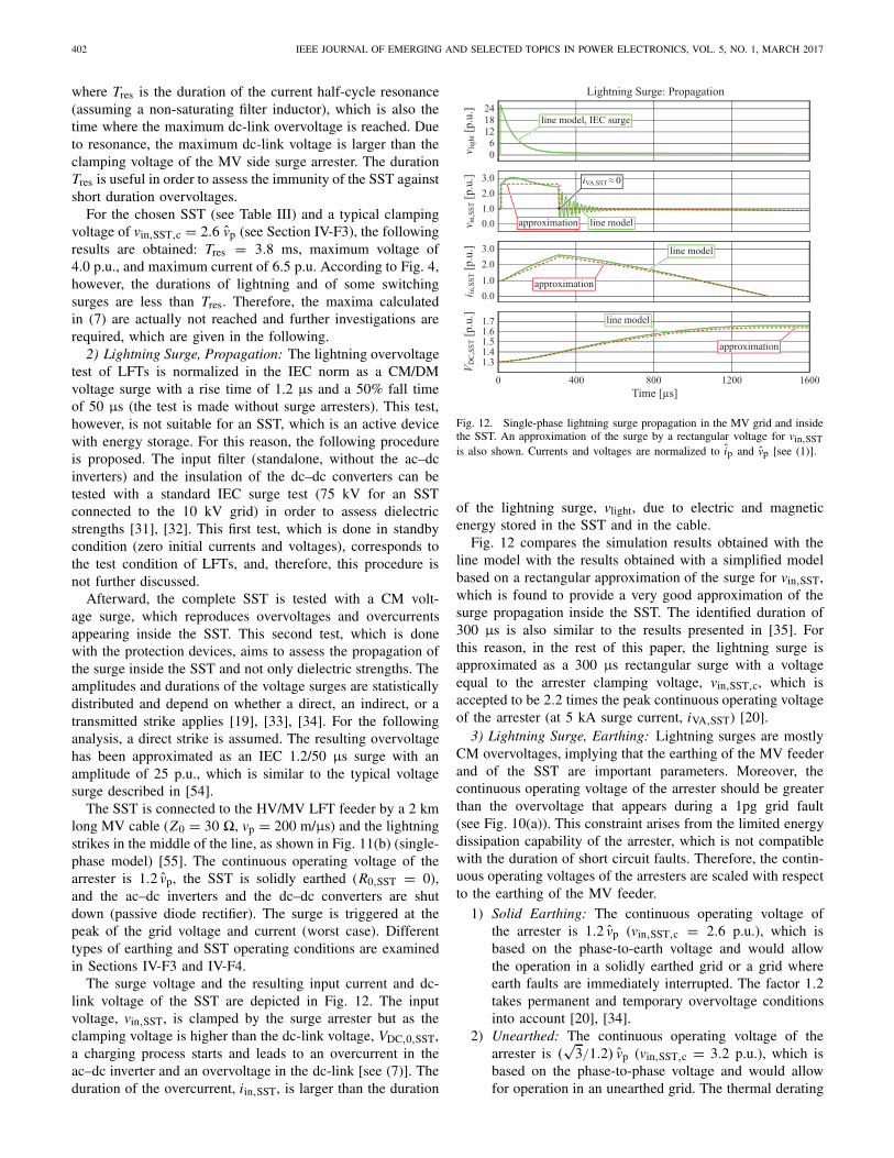
For the chosen SST (see Table III) and a typical clampingvoltage of vin,SST,c = 2.6 vp (see Section IV-F3), the followingresults are obtained: Tres = 3.8 ms, maximum voltage of4.0 p.u., and maximum current of 6.5 p.u. According to Fig. 4,however, the durations of lightning and of some switchingsurges are less than Tres. Therefore, the maxima calculatedin (7) are actually not reached and further investigations arerequired, which are given in the following.
2) Lightning Surge, Propagation: The lightning overvoltagetest of LFTs is normalized in the IEC norm as a CM/DMvoltage surge with a rise time of 1.2 µs and a 50% fall timeof 50 µs (the test is made without surge arresters). This test,however, is not suitable for an SST, which is an active devicewith energy storage. For this reason, the following procedureis proposed. The input filter (standalone, without the ac–dcinverters) and the insulation of the dc–dc converters can betested with a standard IEC surge test (75 kV for an SSTconnected to the 10 kV grid) in order to assess dielectricstrengths [31], [32]. This first test, which is done in standbycondition (zero initial currents and voltages), corresponds tothe test condition of LFTs, and, therefore, this procedure isnot further discussed.
Afterward, the complete SST is tested with a CM volt-age surge, which reproduces overvoltages and overcurrentsappearing inside the SST. This second test, which is donewith the protection devices, aims to assess the propagation ofthe surge inside the SST and not only dielectric strengths. Theamplitudes and durations of the voltage surges are statisticallydistributed and depend on whether a direct, an indirect, or atransmitted strike applies [19], [33], [34]. For the followinganalysis, a direct strike is assumed. The resulting overvoltagehas been approximated as an IEC 1.2/50 µs surge with anamplitude of 25 p.u., which is similar to the typical voltagesurge described in [54].
The SST is connected to the HV/MV LFT feeder by a 2 kmlong MV cable (Z0 = 30 �, vp = 200 m/µs) and the lightningstrikes in the middle of the line, as shown in Fig. 11(b) (single-phase model) [55]. The continuous operating voltage of thearrester is 1.2 vp, the SST is solidly earthed (R0,SST = 0),and the ac–dc inverters and the dc–dc converters are shutdown (passive diode rectifier). The surge is triggered at thepeak of the grid voltage and current (worst case). Differenttypes of earthing and SST operating conditions are examinedin Sections IV-F3 and IV-F4.
The surge voltage and the resulting input current and dc-link voltage of the SST are depicted in Fig. 12. The inputvoltage, vin,SST, is clamped by the surge arrester but as theclamping voltage is higher than the dc-link voltage, VDC,0,SST,a charging process starts and leads to an overcurrent in theac–dc inverter and an overvoltage in the dc-link [see (7)]. Theduration of the overcurrent, iin,SST, is larger than the duration
Fig. 12. Single-phase lightning surge propagation in the MV grid and insidethe SST. An approximation of the surge by a rectangular voltage for vin,SSTis also shown. Currents and voltages are normalized to ip and vp [see (1)].
of the lightning surge, vlight, due to electric and magneticenergy stored in the SST and in the cable.
Fig. 12 compares the simulation results obtained with theline model with the results obtained with a simplified modelbased on a rectangular approximation of the surge for vin,SST,which is found to provide a very good approximation of thesurge propagation inside the SST. The identified duration of300 µs is also similar to the results presented in [35]. Forthis reason, in the rest of this paper, the lightning surge isapproximated as a 300 µs rectangular surge with a voltageequal to the arrester clamping voltage, vin,SST,c, which isaccepted to be 2.2 times the peak continuous operating voltageof the arrester (at 5 kA surge current, iVA,SST) [20].
3) Lightning Surge, Earthing: Lightning surges are mostlyCM overvoltages, implying that the earthing of the MV feederand of the SST are important parameters. Moreover, thecontinuous operating voltage of the arrester should be greaterthan the overvoltage that appears during a 1pg grid fault(see Fig. 10(a)). This constraint arises from the limited energydissipation capability of the arrester, which is not compatiblewith the duration of short circuit faults. Therefore, the contin-uous operating voltages of the arresters are scaled with respectto the earthing of the MV feeder.
1) Solid Earthing: The continuous operating voltage ofthe arrester is 1.2 vp (vin,SST,c = 2.6 p.u.), which isbased on the phase-to-earth voltage and would allowthe operation in a solidly earthed grid or a grid whereearth faults are immediately interrupted. The factor 1.2takes permanent and temporary overvoltage conditionsinto account [20], [34].
2) Unearthed: The continuous operating voltage of thearrester is (
√3/1.2) vp (vin,SST,c = 3.2 p.u.), which is
based on the phase-to-phase voltage and would allowfor operation in an unearthed grid. The thermal derating

GUILLOD et al.: PROTECTION OF MV CONVERTERS IN THE GRID 403
Fig. 13. (a) Maximum input current and (b) maximum dc-link voltage causedby a lightning surge. Different earthing policies are considered. Currents andvoltages are normalized to ip and vp [see (1)].
factor 1.2 allows the operation with a 1pg fault duringapproximately 10 s [20], [34].
3) Resistance Earthing: For a resistance earthing the con-tinuous operating voltage is scaled between the valueschosen for the solidly earthed and the unearthed grid.Between these two extrema, the scaling is done withthe curve for the 1pg fault depicted in Fig. 10(a).
Fig. 13 shows overcurrents and overvoltages in the SST inthe event of a lightning surge and for different realizationsof the MV feeders and the SST’s earthings. The lightningsurge is modeled according to Section IV-F2. If the SST isunearthed, the overvoltage is applied between the star-point ofthe SST and the earth (CM surge). In this case the completeSST reference potential is shifted, which has an impact onthe insulation coordination but not on the ac–dc inverters [16].However, the rapid shift on the star-point potential can producecapacitive disturbances inside the SST [39], [53]. As it is foundthat the stress is larger for a solidly earthed SST, where noshift of the star-point is possible, only this case will be furtherconsidered, together with a solidly earthed MV feeder.
4) Lightning Surge, Converter State: Until now, theac–dc inverter has been considered as a passive diode rectifier.However, an SST features an active inverter that can providea voltage, vAC,SST, between ±VDC,SST at its ac port. Ifthe applied voltage vAC,SST has the same sign as the surgevoltage vin,SST, the voltage across the input inductor will bemoderate [39], [40]. In the case of opposite signs, a largevoltage is applied to the input inductor, leading to a rapidincrease in the input current. A passive diode rectifier willalways produce the best possible voltage, vAC,SST, in order tominimize the impact of the surge.
Fig. 14 illustrates the impact of the inverter state on thesurge propagation inside the SST. The worst possible case(vAC,SST = −VDC,SST, given that vin,SST > 0) is presented andcompared to the case of a passive rectifier (with two differentinitial currents). The active inverter is programmed to shutdown when the input current iin,SST reaches twice the nominalpeak current ip. Thereafter, the inverter is also operated as adiode rectifier. The lightning surge and the SST are modeledaccording to Section IV-F3 (solid earthing).
The shapes of the current and voltage waveforms do notchange fundamentally between active and passive rectifiers.For an SST in standby, the overvoltage and overcurrent areless critical as the initial current is zero. With the nominal
Fig. 14. Impact of the initial converter state on the propagation of a lightningsurge inside the SST. The worst case scenario (active inverter) is presentedtogether with the case of a passive diode rectifier (with two different initialcurrents). Currents and voltages are normalized to ip and vp [see (1)].
Fig. 15. Maximum input current during (a) lightning and (b) switchingsurges. Maximum dc-link voltage during (c) lightning and (d) switchingsurges. Different values of SCRSST and CERSST are considered. Currentsand voltages are normalized to ip and vp [see (1)].
current as initial condition, the stress is higher for the case ofan active inverter compared to a passive rectifier. The maximalinput current increases from 2.5 to 3.2 p.u. and the dc-linkvoltage from 1.65 to 1.75 p.u. However, the detection of thesurge can be drastically improved if the derivative of the inputcurrent, iin,SST, is considered. In this case, the overcurrentsand overvoltages are similar to those obtained with a passiverectifier. For this reason, the state of the inverter will not befurther considered in Sections IV-F5 and IV-F6.
5) Lightning Surge, SST Properties: Fig. 15(a) and (c)shows the maximal input current and dc-link voltage owing toa lightning surge for different values of SCRSST and CERSST.The lightning surge and the SST are modeled according toSection IV-F3 (solid earthing).

404 IEEE JOURNAL OF EMERGING AND SELECTED TOPICS IN POWER ELECTRONICS, VOL. 5, NO. 1, MARCH 2017
The maximum input current mainly depends on the SCRSST,which is explained by the fact that the dc-link voltage remainsapproximately constant during the fast current rise (as longas the surge duration is much smaller than the duration ofthe half-cycle resonance, see (7)). Furthermore, the dc-linkovervoltage mainly depends on the value of CERSST. It canbe seen that the overcurrents produced by a lightning surgeare acceptable (see Section IV-A), while CERSST > 1.0 p.u.is sufficient to maintain the dc-link voltage below 1.7 p.u.,which is also compatible with the voltage utilization of semi-conductors defined in Section IV-A.
6) Switching Surge, SST Properties: The switching surgetest of LFTs is normalized in the IEC norm as a DM voltagesurge with a rise time of 250 µs and a 50% fall time of2500 µs [31], [32]. However, this test is only specified for gridvoltages above 115 kV. In this paper, an adapted model for theMV grid is assumed: a DM 250/2500 µs surge is triggered atthe peaks of the grid voltage and current. The maximum phase-to-phase voltage reaches (2.5
√3) vp [56], [57]. The factor 2.5
defines the maximum voltage that can be applied without beingeffectively clamped by the surge arresters placed between thephases (see Section IV-F3).
As the earthing does not play a fundamental role during aDM surge, a single-phase model is used (with R0,eq,SST = 0,see Fig. 11(a)). The source of the surge is located at the inputof the SST as shown in Fig. 11(c) and vswitch equal to half thephase-to-phase voltage (maximum voltage of (2.5
√3/2) vp).
The inverter is modeled as a passive diode rectifier.Fig. 15(b) and (d) illustrates the input current and
dc-link voltage owing to a switching surge for different valuesof SCRSST and CERSST. The results show that switchingsurges are much more critical than lightning surges due totheir longer durations. This holds particularly true for theinput current, where large RMS currents during the surgecan damage the ac–dc inverter [12], [39], [40]. This currentis flowing in the antiparallel diode of the switches after theshutdown of the ac–dc inverters, implying that the currentrating of the diodes has to be considered. The filter induc-tance, represented with SCRSST, needs to be large enough toavoid high inrush currents, in particular in the case of largedc-link capacitance [see (7)]. The saturation current of thefilter should be selected appropriately or a possible decreasein the filter impedance due to the partial saturation shouldbe taken into account. Furthermore, for small CERSST, thedc-link overvoltage is higher than the surge peak voltage dueto resonance [see (7)].
For the chosen SST (see Table III), the overcurrent is4.0 p.u. while the dc-link voltage reaches 2.6 p.u., which wouldrequire a large overrating of the SST. Even a more robust SST(SCRSST = 10%, CVRSST = 1.5, CERSST = 2.0), will stillexperience an overcurrent of 3.0 p.u. and an overvoltage of2.3 p.u.. This implies that the switching surge is the mostcritical event for an SST connected to the MV grid withclassical protection devices.
G. Advanced Protection Schemes
Different approaches are possible to circumvent the needfor high values of CERSST, CVRSST, and SCRSST. A first
solution is the suppression or mitigation of the transients inthe MV grids. For example, switching transients can be almostsuppressed if the breaker’s actions are synchronized with thephase of the grid voltages [58]. However, transients due tolightning or unpredictable faults cannot be avoided. A secondsolution is the use of advanced protection devices, which offerbetter protection at the MV side as follows.
1) An ultrafast solid-state breaker can be employedto immediately disconnect the SST from the MVgrid during a short circuit or an overvoltagecondition [12], [45], [59]. The main drawbacks ofthis solution are increased conduction losses, cost, andhigh complexity of the protection scheme.
2) A solid-state current limiter can be installed in the MVgrid in order to increase the short circuit impedanceduring a fault [59], [60].
3) For the mitigation of overvoltages, surge capacitorsplaced at the input of the SST are a common solutionto smooth the surges [42], [61]. However, the reactivepower consumption of the capacitors has to be compen-sated for by the SST and, therefore, increases the losses.
4) A spark gap, placed in parallel with the surge arrester,can be used for providing a crowbar protection at theinput of the SST [62]. The main drawback is the createdshort circuit and the fact that the breakdown voltage isnot well-defined for fast transients.
5) A dc brake chopper (or TVS diodes, varistors) canbe used to clamp the dc-link voltages [63], [64]. Thissolution limits the dc-link overvoltages but increases theinrush currents through the ac–dc converters, which arealready critical (see Section IV-F6).
6) An ac crowbar is inserted between the filter andthe inverter [65]. This solution prevents overcurrentsthrough the ac–dc converters without adding lossesduring nominal operation. The main drawback is thatthe grid will experience a short circuit during a half-grid period.
Among these solutions, the solid-state breaker and theac crowbar seem to be the most promising concepts and arepart of the advanced protection scheme depicted in Fig. 16(a).The solid-state breaker is realized by an antiseries connectionof two switches. The breaker has to commutate an inductivecurrent and, therefore, the voltage across the semiconductorsis clamped by a parallel varistor [45], [59]. As the breakershould be able to isolate voltages of up to
√3vp (see Fig. 10),
the varistor will clamp at approximately 2.2√
3vp. In order toachieve the corresponding blocking voltage, a series connec-tion of many devices is required (IGBTs or MOSFETs), which,however, could be optimized for low conduction losses. Theac crowbar consists of two antiparallel thyristors with a seriesresistor (or inductor). The resistor limits the current, however,the maximal voltage drop needs to be less than the dc-linkvoltage [see (5), (7)], in order to ensure zero input current ofthe inverter.
These two protection devices are evaluated during an MVlightning surge according to Section IV-F3 (solidly earthedLFT and SST). A lightning surge has been taken as thisfault leads to the fastest transients and, thus, requires the

GUILLOD et al.: PROTECTION OF MV CONVERTERS IN THE GRID 405
Fig. 16. (a) Advanced protection schemes for the MV side including asurge arrester (VA), an solid-state breaker (SSB), and ac crowbar (ACC).(b) Lightning surge propagation inside the SST with the classical (VA) andadvanced (VA + SSB, VA + ACC) protection schemes. Currents and voltagesare normalized to ip and vp [see (1)].
fastest protection devices. The resulting waveforms can beseen in Fig. 16(b) for the classical and the advanced protectionschemes. The solid-state protection devices are triggered oncethe input current reaches 2 p.u.
The solid-state breaker cannot immediately interrupt theinput current because voltage across the breaker is limited bythe parallel varistor and the remaining voltage is applied tofilter and inverter. However, as the current commutation occursin less than 150 µs, the SST is sufficiently protected againstovervoltages. With the crowbar protection device, the currentcommutates immediately, as the ac–dc inverter path is lowinductive and the dc-link voltage stops to rise. However, due tothe resulting filter short circuit, the input current continues torise (see Section IV-E2). The resulting fault will be cleared atthe next zero crossing of the grid current. This can be avoidedif bidirectional turn-off switches are used in place of thyristors.
V. DESIGN GUIDELINES
A. General Guidelines
From the presented analysis of the 10 kV, 1 MVA SSTshown in Fig. 1, some design guidelines can be extracted(protection scheme according to Fig. 6). These guidelinesmay be subject to modifications if different ratings, convertertopologies, or usages in the grid (industrial, residential, etc.)are considered. The following fault situations must be consid-ered and are modeled as follows.
1) The LV inverter needs to inject enough fault currentin order to trip the downstream protection devices(see Section IV-C). An overcurrent capability of 3× therated current for some seconds should be considered fortripping a sensitive breaker, while a fuse will require
even larger currents. For the complete SST (MV and LVsides), an overload capability of 1.5× for some minutesis typical (see Section IV-A).
2) The internal failure of the MV side of the SST ismodeled with a 3p fault placed right after the filter of theSST (see Section IV-E2). An LFT with the same powerrating feeds the SST. Related investigations indicate thata minimum short circuit impedance of SCRSST ≈ 10%is required, which is larger than the minimum specifiedby the IEC norm. The filter inductor should be able towithstand a short circuit for some hundred milliseconds.As a consequence, sufficiently high saturation currentsand/or the reduction of the filter impedance due to partialsaturation need to be considered.
3) MV grid short circuits are modeled with a 1pg fault(see Section IV-E3). The SST, which is turned off,is fed by an LFT with the same power rating. Forsome earthing policies (low EIRSST and large EIRLFT(see Fig. 10)), the dc-links and the semiconductorsshould be rated for the phase-to-phase voltage. A highohmic MV earthing of the SST is preferred if such anearthing is compatible with the MV grid policies.
4) The dielectric strengths of the different components(filter, medium-frequency transformers, etc.) are testedwith a standard IEC 1.2/50 µs impulse voltage(see Section IV-F2). This test is done without protectiondevices.
5) Lightning surges are modeled with a 300 µs CM rectan-gular pulse with a voltage equal to the arrester clampingvoltage (see Section IV-F2). The test is done for thecomplete SST under nominal operating conditions. Thisleads to the following requirements: the MV powersemiconductors need to be capable to block 1.8× thenominal phase-to-earth peak voltage, the MV dc-linkcapacitances and the filter inductance should be suffi-ciently large (e.g., CERSST > 1.0 and SCRSST > 5%),and the voltage applied to the insulation can reach 3×the nominal phase-to-earth voltage. However, a highohmic MV earthing reduces the impact of CM over-voltages on the SST (see Section IV-F3).
6) Switching surges are modeled with an IEC 250/2500 µsDM pulse with a peak voltage equal to 2.5× the phase-to-phase voltage (see Section IV-F6). The test is done forthe complete SST under nominal condition. Comparedto lightning surges, this type of overvoltage is criticaland imposes SCRSST > 7% and CERSST > 1.75.A large dc-link capacitance, however, demands for asufficiently high filter inductance to avoid large inrushcurrents. Moreover, the MV inverters (i.e., the powerdevices) should be able to accept at least 4× the ratedcurrent and 2.5× the nominal phase peak voltage forsome milliseconds, which is also larger than the valuesobtained for lightning surges.
Similar derating factors have been found for SSTs in tractionapplications [7]. For the cases where the SST cannot reason-ably reach these requirements, advanced protection devicesneed to be considered (see Section IV-G). The solid-statebreaker offers a complete protection against short circuits and

406 IEEE JOURNAL OF EMERGING AND SELECTED TOPICS IN POWER ELECTRONICS, VOL. 5, NO. 1, MARCH 2017
Fig. 17. Impact of the protection requirements on the SST MV side characteristic properties. The following figures of merit are shown: Isw, the currentrating of the MV ac–dc inverters’ semiconductors, Vmax, the blocking voltage of the MV ac–dc inverters (of all cells, per phase), LSST, the inductance of thefilters (per phase), CSST, the dc-link capacitance (of all cells, per phase), Asw, the total chip area, ncell, the number of cells per phase, VL ,SST, the volumeof the filter inductors, and VC,SST, the volume of the dc-link capacitors (of all cells).
overvoltages at the expense of increased losses and complexityand the ac crowbar represents a cheaper and lossless solution,which, however, creates a short circuit for one half-grid period.
B. Case Study: 10 kV/1 MVA Multicell SST
The multicell SST depicted in Fig. 1 is considered with thefollowing ratings: 10 kV, 1 MVA, and 50 Hz [4]. A first design,without protection considerations, is chosen, which consistsof nine cells (per phase) based on 100 A/1700 V IGBTsoperated at 1 kHz and 1200 V (ac–dc inverters). The dc-linkcapacitance is determined by the voltage ripple requirementand the filter inductance by the IEEE 519 standard [66], asdescribed in [13]. In a second step, this design is adapted formeeting the aforementioned protection requirements, which,due to the great number of available degrees of freedom(the number of cells, the switching frequency, the modula-tion index, etc.), can be achieved by different means and issubject to further design objectives, e.g., high power densityor efficiency. In a straightforward manner, the first designcan be modified according to tradeoffs given in [4] and [13].The corresponding result is shown in Fig. 17 for theMV sides of the unmodified (unprotected) and the adapteddesigns.
The filter inductance value required for the protection ofthe SST is about twice the value required for harmonicsfiltering. This has, together with the required overcurrentrating, a decisive impact on the volume of the inductor, whichis computed with the scaling laws presented in [67]. Thisdrastically limits the incentive of increasing the switchingfrequency or the number of levels. Furthermore, the bandwidthof the current control loop, which is inversely proportionalto the inductance of the filter, is reduced by the protectionrequirements [68]. The required dc-link capacitance is alsohigher than the value prescribed by the voltage ripple limit.This, together with the increased blocking voltage, increasesthe volume of the dc-link capacitors. In order to meet theovervoltage and overcurrent requirements, 12 cells based on200 A/1700 V devices have to be considered (or 7 cells basedon 200 A/3300 V devices), which increases the complexity ofthe SST. This infers that the chip area is approximately twicethe value required for nominal operation, which has a directimpact on the cost of SSTs [4]. It is thus concluded that the
protection requirements have a nonnegligible impact on thevolume, weight, and costs of SSTs.
VI. CONCLUSION
This paper proposes a protection scheme for ac–acdistribution-type SSTs. Design criteria and limitations withrespect to current and voltage stresses are investigated, in par-ticular, with respect to robust operation in the MV grid. In thiscontext, different short circuit failure types and overvoltagescenarios are analyzed with the result that MV phase-to-earthshort circuits and MV slow front overvoltage situations areparticularly critical. Furthermore, the MV side earthing of thegrid is found to have a decisive impact on the stresses inthe case of short-circuit failures and overvoltages. On the lowvoltage side, the main challenge is not to protect the SST itselfbut to respect the selectivity of the downstream protectiondevices.
The required overcurrent and overvoltage capabilities needto be taken into account for the design of an SST and have animpact on the achieved efficiency, power density, volume, andcost. It can be concluded that the key design parameters of anSST are not primarily influenced by the rated operation of thesystem, but by the operation during faults. In this context, ahigh switching frequency may not reduce the volume requiredfor the protective circuits and the MV side filter of the SST.The impact will be particularly important for designs withlow power rating, high switching frequency, or high voltageutilization of power devices. Alternatively, a less robust SSTmay be considered if advanced protection devices, such assolid-state circuit breakers, are used. In any case, the protectionscheme and the corresponding derating of the SST have to beconsidered for the optimization and design procedures.
The presented results indicate that SSTs may be bettersuited for operation inside a smart or industrial grid thanfor operation as classical distribution transformers. Inside asmart grid or industrial grid, the dynamics of the sources andloads are known, which reduces the stresses applied to theSSTs. Furthermore, a central protection unit can be used atthe interconnection point between the smart/industrial grid andthe distribution/transmission grid. Yet, the presented investi-gations demonstrate the feasibility of the protection of SSTsand can be further developed with respect to the protection

GUILLOD et al.: PROTECTION OF MV CONVERTERS IN THE GRID 407
of SSTs for specific applications, e.g., SSTs operated insidedc or smart grids. In the case of a well-defined application,a more accurate modeling of faults, in particular by meansof electromagnetic transient simulation may be feasible. Thiswill enable the extraction of more detailed and granular designrules for a particular SST.
REFERENCES
[1] W. McMurray, “Power converter circuits having a high frequency link,”U.S. Patent 3 581 212, Jun. 23, 1970.
[2] J. W. Kolar and G. Ortiz, “Solid-state-transformers: Key components offuture traction and smart grid systems,” in Proc. Int. Power Electron.Conf. (IPEC), May 2014, pp. 1–14.
[3] A. Q. Huang, M. L. Crow, G. T. Heydt, J. P. Zheng, and S. J. Dale, “Thefuture renewable electric energy delivery and management (FREEDM)system: The energy Internet,” Proc. IEEE, vol. 99, no. 1, pp. 133–148,Jan. 2011.
[4] J. E. Huber and J. W. Kolar, “Volume/weight/cost comparison of a1MVA 10 kV/400 V solid-state against a conventional low-frequencydistribution transformer,” in Proc. IEEE Energy Convers. Congr.Expo. (ECCE), Sep. 2014, pp. 4545–4552.
[5] S. Madhusoodhanan, S. Bhattacharya, and K. Hatua, “Control techniquefor 15 kV SiC IGBT based active front end converter of a 13.8 kVgrid tied 100 kVA transformerless intelligent power substation,” in Proc.IEEE Energy Convers. Congr. Expo. (ECCE), Sep. 2013, pp. 4697–4704.
[6] B. Hafez, H. S. Krishnamoorthy, P. Enjeti, S. Ahmed, and I. J. Pitel,“Medium voltage power distribution architecture with medium frequencyisolation transformer for data centers,” in Proc. IEEE Appl. PowerElectron. Conf. Expo. (APEC), Mar. 2014, pp. 3485–3489.
[7] C. Zhao et al., “Power electronic traction transformer—Medium voltageprototype,” IEEE Trans. Ind. Electron., vol. 61, no. 7, pp. 3257–3268,Jul. 2014.
[8] M. Steiner and H. Reinold, “Medium frequency topology in rail-way applications,” in Proc. Eur. Conf. Power Electron. Appl. (EPE),Sep. 2007, pp. 1–10.
[9] P. Tatcho, H. Li, Y. Jiang, and L. Qi, “A novel hierarchical sectionprotection based on the solid state transformer for the future renewableelectric energy delivery and management (FREEDM) system,” IEEETrans. Smart Grid, vol. 4, no. 2, pp. 1096–1104, Jun. 2013.
[10] T. Guillod, F. Krismer, R. Färber, C. M. Franck, and J. W. Kolar,“Protection of MV/LV solid-state transformers in the distribution grid,”in Proc. Ind. Electron. Soc. Conf. (IECON), Nov. 2015, pp. 3531–3538.
[11] Z. Wang, J. Xu, K. Hatua, S. Madhusoodhanan, and S. Bhattacharya,“Solid state transformer specification via feeder modeling and simula-tion,” in Proc. IEEE Power Energy Soc. General Meeting, Jul. 2012,pp. 1–5.
[12] S. Madhusoodhanan, D. Patel, S. Bhattacharya, J. A. Carr, and Z. Wang,“Protection of a transformerless intelligent power substation,” in Proc.IEEE Power Electron. Distrib. Generat. Syst. Symp. (PEDG), Jul. 2013,pp. 1–8.
[13] J. E. Huber and J. W. Kolar, “Optimum number of cascaded cellsfor high-power medium-voltage multilevel converters,” in Proc. IEEEEnergy Convers. Congr. Expo. (ECCE), Sep. 2013, pp. 359–366.
[14] X. She, R. Burgos, G. Wang, F. Wang, and A. Q. Huang, “Review ofsolid state transformer in the distribution system: From components tofield application,” in Proc. IEEE Energy Convers. Congr. Expo. (ECCE),Sep. 2012, pp. 4077–4084.
[15] D. Rothmund, G. Ortiz, and J. W. Kolar, “SiC-based unidirectional solid-state transformer concepts for directly interfacing 400V DC to medium-voltage AC distribution systems,” in Proc. IEEE Telecommun. EnergyConf. (INTELEC), Sep./Oct. 2014, pp. 1–9.
[16] T. Guillod, J. E. Huber, G. Ortiz, A. De, C. M. Franck, and J. W. Kolar,“Characterization of the voltage and electric field stresses in multi-cell solid-state transformers,” in Proc. IEEE Energy Convers. Congr.Expo. (ECCE), Sep. 2014, pp. 4726–4734.
[17] MV/LV transformer substations: Theory and examples of short-circuitcalculation, ABB, Bergamo, Italy, 2008.
[18] D. Fulchiron, “Protection of MV/LV substation transformers,” Schneider,Grenoble, France, Tech. Rep. 192, 2008.
[19] D. Fulchiron, “Overvoltages and insulation coordination in MV andHV”, Merlin Gerin, Grenoble, France, Tech. Rep. 151, 1995.
[20] Overvoltage protection, metal oxide surge arresters in medium voltagesystems, ABB, Wettingen, Switzerland, 2011.
[21] Electrical installation guide, Protection against voltage surges in LV,Schneider, Rueil-Malmaison, France, 2008.
[22] R. Smeets, L. van der Sluis, M. Kapetanovic, D. F. Peelo, andA. Janssen, Switching in Electrical Transmission and Distribution Sys-tems. New York, NY, USA: Wiley, 2014.
[23] Protection and control, Protection guide, Merlin Gerin, Grenoble,France, 1996.
[24] N. Tleis, Power Systems Modelling and Fault Analysis: Theory andPractice. Oxford, U.K.: Newnes, 2007.
[25] Totally Integrated Power, System protection/Safety Coordination, 2nd ed.Siemens, Munich, Germany, 2005.
[26] Low-Voltage Switchgear and Controlgear, document IEC-60947, 2011.[27] ABB Switchgear Manual, 11th ed., ABB, Mannheim, Germany, 2006.[28] Short-Circuit Currents in Three-Phase A.C. Systems, document
IEC-60909, 2001.[29] A. J. Schwab, Elektroenergiesysteme: Erzeugung, Transport, Übertra-
gung und Verteilung elektrischer Energie, (in German). Springer, Berlin,Germany, 2012.
[30] Insulation Coordination, document IEC-60071, IEC, 2006.[31] Power Transformers, document IEC-60076, IEC, 2011.[32] High-Voltage Test Techniques, document IEC-60060, IEC, 2010.[33] A. Porrino et al., “Protection of MV and LV networks against light-
ning. I. Basic information,” in Proc. Conf. Electr. Distrib. (CIRED),vol. 1. Jun. 1997, pp. 21/1–21/7.
[34] A. Porrino et al., “Lightning protection of distribution net-works. II. Application to MV networks,” in Proc. Conf. Electr. Dis-trib. (CIRED), vol. 1. Jun. 1997, pp. 28/1–28/8.
[35] M. S. Savic, “Estimation of the surge arrester outage rate causedby lightning overvoltages,” IEEE Trans. Power Del., vol. 20, no. 1,pp. 116–122, Jan. 2005.
[36] IEC Standard Voltages, Standard IEC-60038, 2009.[37] ANSI Guide for Loading Mineral-Oil-Immersed Power Transformers,
ANSI C57.92-1962, 1962[38] B. Lacrois and R. Calvas, “Earthing systems worldwide and evolutions”,
Merlin Gerin, Grenoble, France, Tech. Rep. 173, 1995.[39] J. Carr, Z. Wang, S. Bhattacharya, and D. Patel, “Transient overvoltage
rating and BIL of the transformerless intelligent power substation,” inProc. IEEE Power Energy Soc. General Meeting, Jul. 2013, pp. 1–5.
[40] J. Carr, Z. Wang, S. Bhattacharya, K. Hatua, and S. Madhusoodhanan,“Overloading and overvoltage evaluation of a transformerless intelligentpower substation,” in Proc. IEEE Power Energy Soc. General Meeting,Jul. 2013, pp. 1–5.
[41] B. Backlund, M. Rahimo, S. Klaka, and J. Siefken, “Topologies, voltageratings and state of the art high power semiconductor devices for mediumvoltage wind energy conversion,” in Proc. Power Electron. Mach. WindAppl. Conf. (PEMWA), Jun. 2009, pp. 1–6.
[42] T.-W. Liao and T. H. Lee, “Surge suppressors for the protection of solid-state devices,” IEEE Trans. Ind. Appl., vol. IGA-2, no. 1, pp. 44–52,Jan. 1966.
[43] X. She, A. Q. Huang, S. Lukic, and M. E. Baran, “On integration ofsolid-state transformer with zonal DC microgrid,” IEEE Trans. SmartGrid, vol. 3, no. 2, pp. 975–985, Jun. 2012.
[44] G. G. Karady and X. Liu, “Fault management and protection ofFREEDM systems,” in Proc. IEEE Power Energy Soc. General Meeting,Jul. 2010, pp. 1–4.
[45] O. Vodyakho, M. Steurer, D. Neumayr, C. S. Edrington, G. Karady,and S. Bhattacharya, “Solid-state fault isolation devices: Application tofuture power electronics-based distribution systems,” IET Electr. PowerAppl., vol. 5, no. 6, pp. 521–528, Jul. 2011.
[46] K. Mainali, S. Madhusoodhanan, A. Tripathi, D. Patel, and S. Bhat-tacharya, “Start-up scheme for solid state transformers connected tomedium voltage grids,” in Proc. IEEE Appl. Power Electron. Conf.Expo. (APEC), Mar. 2015, pp. 1014–1021.
[47] J. C. Hernández, P. G. Vidal, and F. Jurado, “Lightning and surge pro-tection in photovoltaic installations,” IEEE Trans. Power Del., vol. 23,no. 4, pp. 1961–1971, Oct. 2008.
[48] C. Rodriguez and G. Amaratunga, “Long-lifetime power inverter forphotovoltaic AC modules,” IEEE Trans. Ind. Electron., vol. 55, no. 7,pp. 2593–2601, Jul. 2008.
[49] Low-voltage fuses, Catalogue 2012, Siba, Lünen, Germany, 2012.[50] R. Greul, “Modulare Dreiphasen Pulsgleichrichtersysteme,”
(in German), Ph.D. dissertation, ETH Zurich, Zürich, Switzerland,Dec. 2005.
[51] G. Liang, H. Sun, X. Zhang, and X. Cui, “Modeling of trans-former windings under very fast transient overvoltages,” IEEE Trans.Electromagn. Compat., vol. 48, no. 4, pp. 621–627, Nov. 2006.
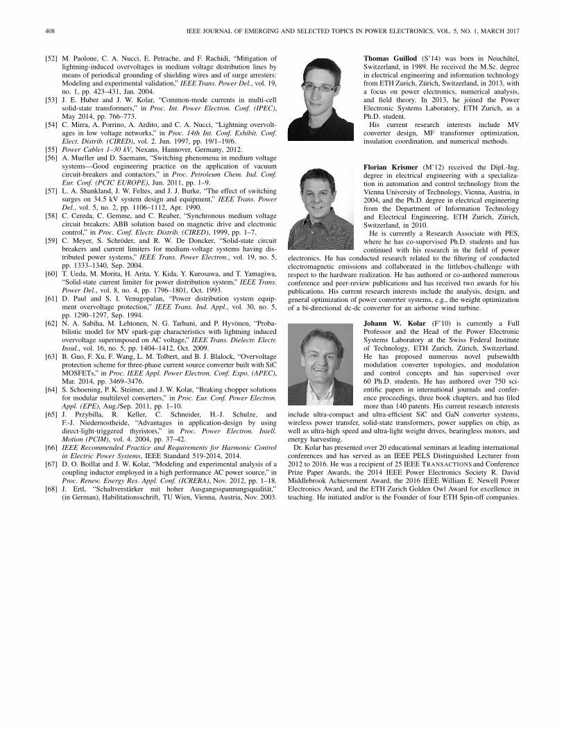
408 IEEE JOURNAL OF EMERGING AND SELECTED TOPICS IN POWER ELECTRONICS, VOL. 5, NO. 1, MARCH 2017
[52] M. Paolone, C. A. Nucci, E. Petrache, and F. Rachidi, “Mitigation oflightning-induced overvoltages in medium voltage distribution lines bymeans of periodical grounding of shielding wires and of surge arresters:Modeling and experimental validation,” IEEE Trans. Power Del., vol. 19,no. 1, pp. 423–431, Jan. 2004.
[53] J. E. Huber and J. W. Kolar, “Common-mode currents in multi-cellsolid-state transformers,” in Proc. Int. Power Electron. Conf. (IPEC),May 2014, pp. 766–773.
[54] C. Mirra, A. Porrino, A. Ardito, and C. A. Nucci, “Lightning overvolt-ages in low voltage networks,” in Proc. 14th Int. Conf. Exhibit. Conf.Elect. Distrib. (CIRED), vol. 2. Jun. 1997, pp. 19/1–19/6.
[55] Power Cables 1–30 kV, Nexans, Hannover, Germany, 2012.[56] A. Mueller and D. Saemann, “Switching phenomena in medium voltage
systems—Good engineering practice on the application of vacuumcircuit-breakers and contactors,” in Proc. Petroleum Chem. Ind. Conf.Eur. Conf. (PCIC EUROPE), Jun. 2011, pp. 1–9.
[57] L. A. Shankland, J. W. Feltes, and J. J. Burke, “The effect of switchingsurges on 34.5 kV system design and equipment,” IEEE Trans. PowerDel., vol. 5, no. 2, pp. 1106–1112, Apr. 1990.
[58] C. Cereda, C. Gemme, and C. Reuber, “Synchronous medium voltagecircuit breakers: ABB solution based on magnetic drive and electroniccontrol,” in Proc. Conf. Electr. Distrib. (CIRED), 1999, pp. 1–7.
[59] C. Meyer, S. Schröder, and R. W. De Doncker, “Solid-state circuitbreakers and current limiters for medium-voltage systems having dis-tributed power systems,” IEEE Trans. Power Electron., vol. 19, no. 5,pp. 1333–1340, Sep. 2004.
[60] T. Ueda, M. Morita, H. Arita, Y. Kida, Y. Kurosawa, and T. Yamagiwa,“Solid-state current limiter for power distribution system,” IEEE Trans.Power Del., vol. 8, no. 4, pp. 1796–1801, Oct. 1993.
[61] D. Paul and S. I. Venugopalan, “Power distribution system equip-ment overvoltage protection,” IEEE Trans. Ind. Appl., vol. 30, no. 5,pp. 1290–1297, Sep. 1994.
[62] N. A. Sabiha, M. Lehtonen, N. G. Tarhuni, and P. Hyvönen, “Proba-bilistic model for MV spark-gap characteristics with lightning inducedovervoltage superimposed on AC voltage,” IEEE Trans. Dielectr. Electr.Insul., vol. 16, no. 5, pp. 1404–1412, Oct. 2009.
[63] B. Guo, F. Xu, F. Wang, L. M. Tolbert, and B. J. Blalock, “Overvoltageprotection scheme for three-phase current source converter built with SiCMOSFETs,” in Proc. IEEE Appl. Power Electron. Conf. Expo. (APEC),Mar. 2014, pp. 3469–3476.
[64] S. Schoening, P. K. Steimer, and J. W. Kolar, “Braking chopper solutionsfor modular multilevel converters,” in Proc. Eur. Conf. Power Electron.Appl. (EPE), Aug./Sep. 2011, pp. 1–10.
[65] J. Przybilla, R. Keller, C. Schneider, H.-J. Schulze, andF.-J. Niedernostheide, “Advantages in application-design by usingdirect-light-triggered thyristors,” in Proc. Power Electron. Intell.Motion (PCIM), vol. 4. 2004, pp. 37–42.
[66] IEEE Recommended Practice and Requirements for Harmonic Controlin Electric Power Systems, IEEE Standard 519-2014, 2014.
[67] D. O. Boillat and J. W. Kolar, “Modeling and experimental analysis of acoupling inductor employed in a high performance AC power source,” inProc. Renew. Energy Res. Appl. Conf. (ICRERA), Nov. 2012, pp. 1–18.
[68] J. Ertl, “Schaltverstärker mit hoher Ausgangsspannungsqualität,”(in German), Habilitationsschrift, TU Wien, Vienna, Austria, Nov. 2003.
Thomas Guillod (S’14) was born in Neuchâtel,Switzerland, in 1989. He received the M.Sc. degreein electrical engineering and information technologyfrom ETH Zurich, Zürich, Switzerland, in 2013, witha focus on power electronics, numerical analysis,and field theory. In 2013, he joined the PowerElectronic Systems Laboratory, ETH Zurich, as aPh.D. student.
His current research interests include MVconverter design, MF transformer optimization,insulation coordination, and numerical methods.
Florian Krismer (M’12) received the Dipl.-Ing.degree in electrical engineering with a specializa-tion in automation and control technology from theVienna University of Technology, Vienna, Austria, in2004, and the Ph.D. degree in electrical engineeringfrom the Department of Information Technologyand Electrical Engineering, ETH Zurich, Zürich,Switzerland, in 2010.
He is currently a Research Associate with PES,where he has co-supervised Ph.D. students and hascontinued with his research in the field of power
electronics. He has conducted research related to the filtering of conductedelectromagnetic emissions and collaborated in the littlebox-challenge withrespect to the hardware realization. He has authored or co-authored numerousconference and peer-review publications and has received two awards for hispublications. His current research interests include the analysis, design, andgeneral optimization of power converter systems, e.g., the weight optimizationof a bi-directional dc-dc converter for an airborne wind turbine.
Johann W. Kolar (F’10) is currently a FullProfessor and the Head of the Power ElectronicSystems Laboratory at the Swiss Federal Instituteof Technology, ETH Zurich, Zürich, Switzerland.He has proposed numerous novel pulsewidthmodulation converter topologies, and modulationand control concepts and has supervised over60 Ph.D. students. He has authored over 750 sci-entific papers in international journals and confer-ence proceedings, three book chapters, and has filedmore than 140 patents. His current research interests
include ultra-compact and ultra-efficient SiC and GaN converter systems,wireless power transfer, solid-state transformers, power supplies on chip, aswell as ultra-high speed and ultra-light weight drives, bearingless motors, andenergy harvesting.
Dr. Kolar has presented over 20 educational seminars at leading internationalconferences and has served as an IEEE PELS Distinguished Lecturer from2012 to 2016. He was a recipient of 25 IEEE TRANSACTIONS and ConferencePrize Paper Awards, the 2014 IEEE Power Electronics Society R. DavidMiddlebrook Achievement Award, the 2016 IEEE William E. Newell PowerElectronics Award, and the ETH Zurich Golden Owl Award for excellence inteaching. He initiated and/or is the Founder of four ETH Spin-off companies.