Properties of GaN epitaxial layers grown on 6H- SiC(0001 ...
20
1 Properties of GaN epitaxial layers grown on 6H- SiC(0001) by plasma-assisted molecular beam epitaxy C. D. Lee, V. Ramachandran, Ashutosh Sagar, and R. M. Feenstra Department of Physics, Carnegie Mellon University, Pittsburgh, Pennsylvania 15213 D. W. Greve Department of Electrical and Computer Engineering, Carnegie Mellon University, Pittsburgh, PA 15213 W. L. Sarney and L. Salamanca-Riba Materials and Nuclear Engineering Department, University of Maryland, College Park, MD 20742-2115 D. C. Look Wright State University and Air Force Research Laboratory, Dayton, Ohio 45435 Song Bai, W. J. Choyke and R. P. Devaty Department of Physics and Astronomy, University of Pittsburgh, Pittsburgh, Pennsylvania 15260 Abstract The structural, electrical, and optical properties of GaN grown on 6H- SiC(0001) substrates by molecular beam epitaxy are studied. Suitable sub- strate preparation and growth conditions are found to greatly improve the structural quality of the films. Threading dislocation densities of about 1 × 10 9 cm -2 for edge dislocations and < 1 × 10 6 cm -2 for screw dislocations are achieved in GaN films of 0.8 μm thickness. Mechanisms of dislocation generation and annihilation are discussed. Increasing the Ga to N flux ratio used during growth is found to improve the surface morphology. An unin- tentional electron concentration in the films of about 5 × 10 17 cm -3 is ob- served, and is attributed to excess Si in the films due to a Si-cleaning step used in the substrate preparation. Results from optical characterization are correlated with the structural and electronic studies. 1 Introduction The large band gap, high breakdown field, and high electron saturation velocity of GaN make it ideal for use in visible-to-UV optoelectronic devices and high speed, high power electronic appli- cations. Almost all such devices developed over the past number of years have been fabricated in material grown by metalorganic chemical vapor deposition (MOCVD). Unfortunately, bulk GaN in wafer sizes is not available, so most growth is performed on sapphire. Despite a lattice mismatch to GaN of about 14%, MOCVD growth on sapphire using an appropriate low-temperature buffer layer yields relatively high quality material. Dislocation densities as low as 7×10 8 cm -2 for thread- ing dislocations which intersect the surface have been reported [1]. The recent innovation of lateral epitaxial overgrowth leads to a reduction in this density by several orders of magnitude in the lat- erally grown regions of the films [2,3], but the process is somewhat complicated. An alternate sub-
Transcript of Properties of GaN epitaxial layers grown on 6H- SiC(0001 ...
ke itppli-ated inaN
matchuffer
laterale lat-sub-
Properties of GaN epitaxial layers grown on 6H-SiC(0001) by plasma-assisted molecular beam epitaxy
C. D. Lee, V. Ramachandran, Ashutosh Sagar, and R. M. FeenstraDepartment of Physics, Carnegie Mellon University, Pittsburgh, Pennsylvania
15213D. W. Greve
Department of Electrical and Computer Engineering, Carnegie Mellon University,Pittsburgh, PA 15213
W. L. Sarney and L. Salamanca-RibaMaterials and Nuclear Engineering Department, University of Maryland, College
Park, MD 20742-2115D. C. Look
Wright State University and Air Force Research Laboratory, Dayton, Ohio 45435Song Bai, W. J. Choyke and R. P. Devaty
Department of Physics and Astronomy, University of Pittsburgh, Pittsburgh,Pennsylvania 15260
Abstract
The structural, electrical, and optical properties of GaN grown on 6H-SiC(0001) substrates by molecular beam epitaxy are studied. Suitable sub-strate preparation and growth conditions are found to greatly improve thestructural quality of the films. Threading dislocation densities of about 1×109 cm-2 for edge dislocations and < 1× 106 cm-2 for screw dislocationsare achieved in GaN films of 0.8µm thickness. Mechanisms of dislocationgeneration and annihilation are discussed. Increasing the Ga to N flux ratioused during growth is found to improve the surface morphology. An unin-tentional electron concentration in the films of about 5× 1017 cm-3 is ob-served, and is attributed to excess Si in the films due to a Si-cleaning stepused in the substrate preparation. Results from optical characterization arecorrelated with the structural and electronic studies.
1 Introduction
The large band gap, high breakdown field, and high electron saturation velocity of GaN maideal for use in visible-to-UV optoelectronic devices and high speed, high power electronic acations. Almost all such devices developed over the past number of years have been fabricmaterial grown by metalorganic chemical vapor deposition (MOCVD). Unfortunately, bulk Gin wafer sizes is not available, so most growth is performed on sapphire. Despite a lattice misto GaN of about 14%, MOCVD growth on sapphire using an appropriate low-temperature blayer yields relatively high quality material. Dislocation densities as low as 7×108 cm-2 for thread-ing dislocations which intersect the surface have been reported [1]. The recent innovation ofepitaxial overgrowth leads to a reduction in this density by several orders of magnitude in therally grown regions of the films [2,3], but the process is somewhat complicated. An alternate
1
randy
Text Box
Published in J. Electronic Materials 30, 162 (2001).
ereprovestrat-
wns prioropysingingbe-
tively,ention-ningscenceclu-
01)lls aressednot
fromflux iseakytterna hy-lf orly-cking
l. Fol-dep-
e oxidewhile
red. Itg.is
islo-isonfor
is per-
strate is SiC, with 3.4% mismatch to GaN. Early work with this material yielded results which wno better than those using sapphire, although recently with the use of H-etching of SiC to imits surface morphology growth of GaN on SiC by molecular beam epitaxy (MBE) has demoned material of relatively high quality, suitable for device applications [4-9].
In this work we report on structural, electrical, and optical characteristics of MBE groGaN on SiC. Details are given of H-etching and Si-cleaning steps used on the SiC substrateto growth. The evolution of the film morphology is monitored using atomic force microsc(AFM) and scanning tunneling microscopy (STM). Dislocations in the film are characterized utransmission electron microscopy (TEM) and high resolution x-ray diffraction (HRXRD), yielda detailed picture of the dislocation generation and annihilation in the films. We distinguishtween high temperature and low temperature growth regimes, 650 C or 600 C respecin discussing the results. Electrical characterization reveals the presence of substantial unintal doping in the material, which is attributed to the presence of Si (arising from the Si-cleastep) as seen in secondary-ion mass spectrometry (SIMS). Low-temperature photolumine(PL) provides information on the point defect concentration in the films and reveals cubic insions in non-optimally prepared material.
2 Experimental
GaN films of typically 0.8µm thickness are deposited by MBE on Si-face on-axis 6H-SiC(00substrates. Activated nitrogen is supplied by an SVTA RF-plasma source, and effusion ceused for Ga and various dopants. Ultra-high purity (99.9999%) nitrogen is used. It is pathrough an Aeronex gas purifier (except for some of our early films, where this purifier wasinstalled) which we find from residual gas analysis is effective at removing oxygen and waterthe source gas. Ga fluxes are measured with a crystal thickness monitor, and the active Ncalibrated by defining the Ga/N flux ratio to be unity at the point where a transition between strand spotty behavior occurs in the reflection high energy electron diffraction (RHEED) pa[10,11]. Hydrogen etching of the SiC is carried out at a temperature of 1600–1700 C withdrogen flow of about 14 liters/min [4]. The H-etching produces a surface with steps of only hafull unit cell height (7.5 or 15 Å for 6H-SiC). As discussed in Section IV, we feel that the 6H potype of SiC is best for GaN epitaxy since these step heights then prevent the formation of stamismatch boundaries [6] which would be encountered for either unetched SiC or 4H materialowing H-etching, the SiC substrates are transferred through air to the MBE chamber. Prior toosition, the samples are first outgassed at about 800 C for 30 minutes. To remove the surfacformed during transfer through air, several monolayers of Si are deposited on the substrateit is near room temperature. It is then annealed at 1000 C and the RHEED pattern is monitostarts at 3×3, then changes to 1×1, and then forms a 3×1 pattern after about an hour of annealinThis latter pattern is indicative of a√3 × √3-R30 surface reconstruction, a structure whichknown to consist of 1/3 monolayer (ML = 1.22× 10¹⁵ atoms/cm2) of Si adatoms on top of a bulk-terminated SiC bilayer [12].
X-ray measurements are performed in the triple-crystal configuration, using Cuα1 radia-tion. TEM is done using a JEOL 4000FX operating at 300 kV. Anisotropic etching to reveal dcations is done using 0.03 M KOH and focused illumination from a Hg arc lamp [13]. Comparof dislocation density from the etching technique with that from TEM was performedMOCVD-grown GaN, and good agreement was obtained between the two methods [14]. PL
>∼ ° <~ °
°
°
°
°
2
4 nmrovide
nglese full
hbor-d the
ently,cribediguresist ofof theteps.ng the1 havelowers barelysometainedthetained.
ing3 MLran-ture.landsted]. AsvectorameaNfor-
Forures,ntainatio,
is 2.9ctional
ation.
formed at a temperature of 2 K, usually using a frequency doubled Ar ion laser producing 24excitation. In specific cases, as noted below, a He-Cd laser operating at 325 nm is used to pa longer absorption length for the excitation.
3 Morphological Evolution During Growth
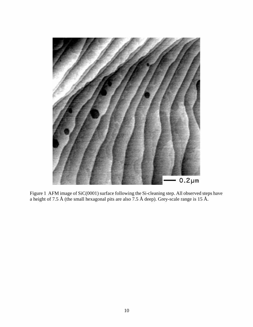
AFM images reveal that the H-etched SiC substrates consist of shallow facets, with facet aless than the unintentional miscut of the wafer [4]. On a single facet all steps are found to havunit cell height, and the steps have normal vectors directed in a <1 00> direction [4]. A neiging facet has step normals directed in another <1 00> direction, rotated 60 from the first, anterraces on that facet are then half a unit cell offset in height from those of the first. Consequhalf unit cell high steps occur at the intersections of the facets. The Si-cleaning procedure desin Section II, used to remove the surface oxide, modifies the surface morphology of the SiC. F1 shows an AFM image obtained after this Si-cleaning step. The morphology is seen to conterraces, which are in this case separated by half unit cell high (7.5 Å) steps. Near the topimage the steps form pairs, and it is apparent that they have formed from full unit cell high sThe Si-cleaning step has apparently produced some etching of the SiC (in addition to removioxide which formed on the surface). The small hexagonal holes seen in the terraces of Fig.depth of half a unit cell. Further etching causes them to merge with the step leading to theterrace, and the step edge then acquires a very irregular shape. One subtle feature which ivisible in Fig. 1 is that the contrast on the terraces themselves is slightly irregular, suggestingnonuniformity of the terraces. STM imaging of the same sample revealed that the surface cona mixture of 3×3 and√3 × √3-R30 surface reconstructions, thus illustrating a problem withSi-cleaning method in that the precise Si coverage (1/3 ML) cannot always be precisely ob
Following the Si-cleaning of the SiC, MBE growth is initiated by simultaneously exposthe substrate to the N and Ga fluxes. Figure 2 shows STM results for the morphology of a 0.thick film, with the deposition performed at 650 C. Nucleation of the film is seen to occurdomly on the SiC terraces. The evolution of the film morphology varies with growth temperaFor high temperature (HT) growth, 650 C, the GaN grows as flat-topped 3-dimensional is[5]. At film thickness of 4 nm the islands havenotcoalesced, whereas we expect from an estimacritical thickness of 2–3 nm that the strain in the GaN has relaxed at that film thickness [15discussed in Section IV, the dislocations which produce this strain relaxation have Burgersb = 1/3 <11 0>, and for thicker films the threading dislocations they give rise to all have that scharacter (i.e.edge dislocations). In contrast, for low temperature (LT) growth, 600 C, the Gfilm at 4 nm thickness completely wets the SiC substrate [5]. This film is strain relaxed by themation of a network of dislocations which give rise to threading dislocations withbothedge andscrew character, as well as possibly some mixed character threading dislocations.
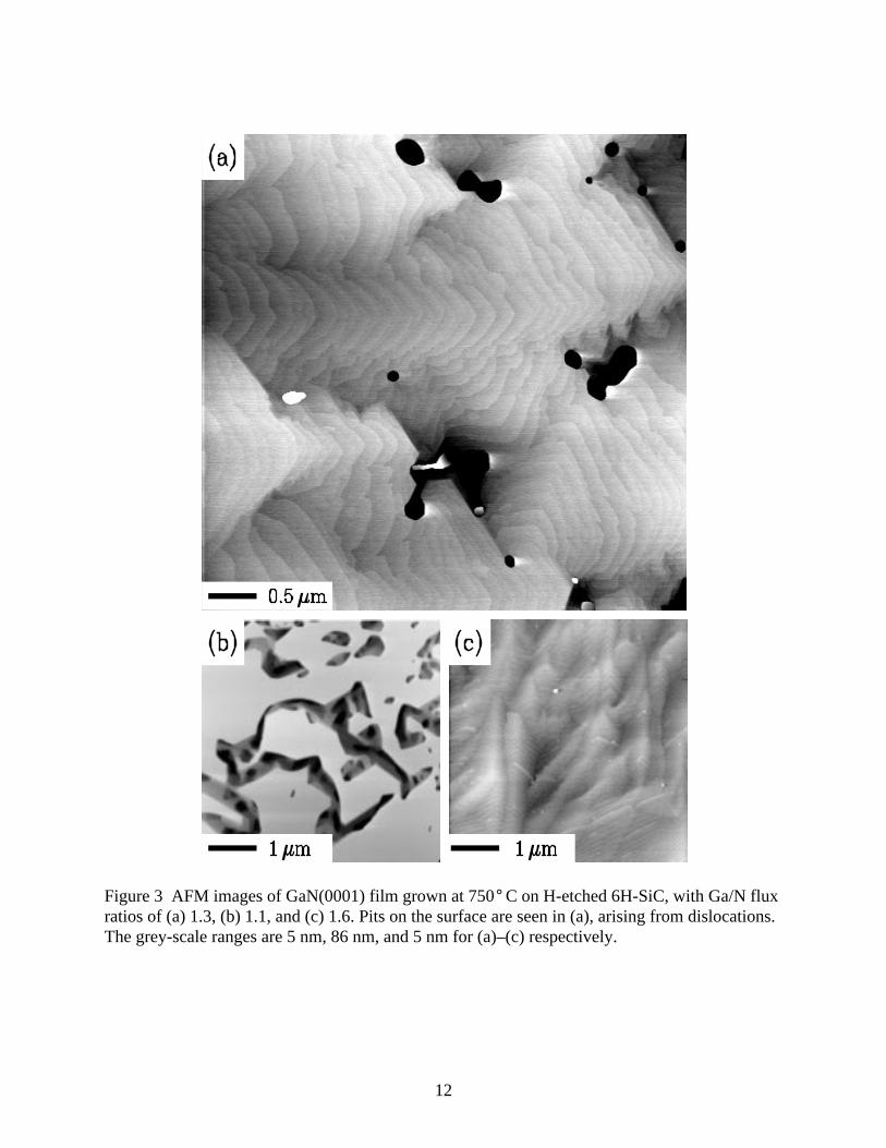
For thicker films, the resulting morphology reflects the dislocation content of the films.LT growth, screw (or mixed) character threading dislocations give rise to spiral growth featas previously presented [5]. HT films display very few spiral growth features since they covery few screw dislocations. The film morphology is also found to depend on the Ga/N flux ras shown in Fig. 3. For moderately Ga-rich conditions, with Ga/N flux≈ 1.3, we find relatively flatfilms interspersed with small pits as shown in Fig. 3(a). The rms roughness for that imagenm, and in regions between the pits the rms roughness is 0.5 nm. From a number of cross-seTEM images we find a correlation of the pit location and the presence of a threading disloc
11 °
°
°
>∼ °
2<~ °
3
dis-. Forhes,.tion of
eamh den-n to re-nsity
t filmntly theaboutcopyhere
ups ofdislo-e at aen-
hbor-am-
hoseagespiralsur-
outnd then-H-e filmsret theon-H-
(L),the
ienta-iCwing
We thus tentatively attribute the pit formation with some sort of equilibrium pit structure nearlocations or perhaps with the decomposition of the GaN during growth near the dislocationlower flux ratios≈ 1.1 the size and number of pits grows, and they often merge to form trencas in Fig. 3(b). Finally, for higher flux ratios≈ 1.6 the pit formation is inhibited, as shown in Fig3(c). In that case, however, Ga droplets start to form on the surface as seen by visual inspecthe films.
4 Structural Characterization
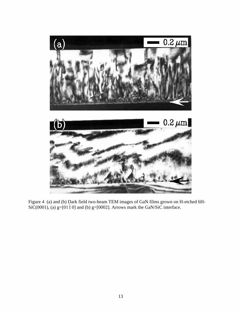
TEM results for an optimized HT growth are shown in Fig. 4; panels (a) and (b) show the two-bimages which are sensitive to threading edge and screw dislocations, respectively [16]. A higsity of edge dislocations is seen near the GaN/SiC interface, and these dislocations are seeduce their number significantly by annihilation as one moves to the surface of the film. The deof threading edge dislocations at the surface is found to be≈ 3 × 109 cm-2, and similar values arefound in other samples. These values are higher than our previously reported density of 2× 10⁸
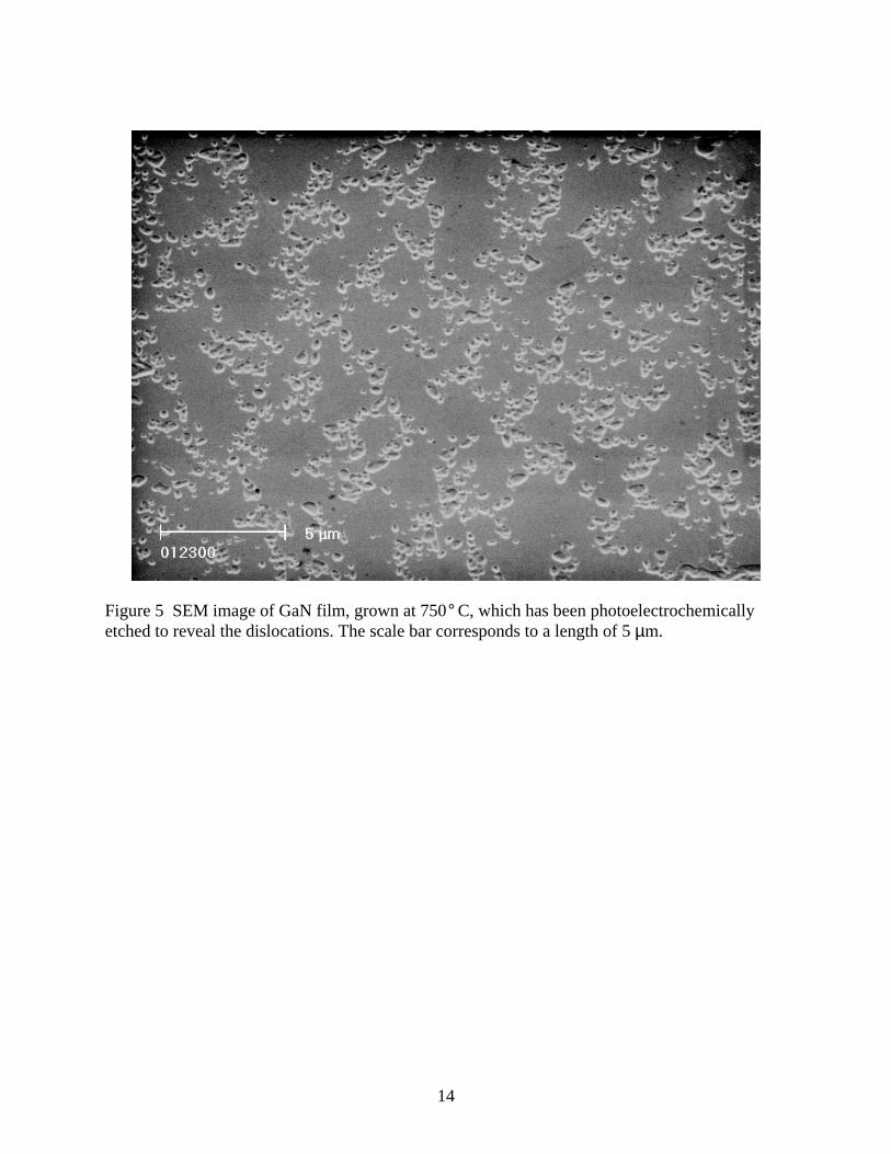
cm-2 [16,17]; some uncertainty in this lower value exists since some of the dislocations in thaterminated in surface pits (rather than the surface plane) and were not counted. Conseque2 × 108 cm-2 value is perhaps an underestimate, and a better value for that earlier sample is8 × 108 cm-2. We have used anisotropic etching and plan view scanning electron micros(SEM) to obtain a more accurate count of dislocation density. Results are shown in Fig. 5, weach protrusion arises from a single dislocation or a small group of dislocations. For the grodislocations, close examination of the image generally allows one to estimate the number ofcations in each group. Counting the dislocation density from this and other images we arrivvalue of 6× 108 cm-2. Combining the SEM and TEM results, we estimate our edge dislocation dsity to be about 1× 109 cm-2.
Concerning threading screw dislocations, none are observed in Fig. 4(b) nor on neiging regions of the film that were imaged by TEM. Similar results were obtained from other sples. From these results we can set an upper bound of < 1× 108 cm-2 for the screw dislocationdensity. A more stringent limit can be obtained by examination of AFM images such as tshown in Fig. 3. Screw dislocations lead to growth spirals, which are easily seen in AFM im[5]. For the case of HT optimized growth such as that shown in Fig. 3, we observe no growth sin an imaged surface area of > 10-6 cm2, leading to a threading screw dislocation density at the sface of < 1× 106 cm-2.
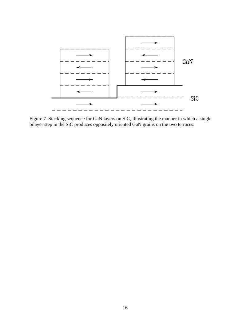
High resolution TEM images are shown in Fig. 6, for HT-growth material, with and withH-etching. The H-etched material shows a well defined interface, with no apparent steps, aGaN film has perfect hexagonal (wurtzite) stacking. In contrast, the film grown on the noetched substrate shows thin regions of cubic (zincblende) stacking near the interface; thesalso show dislocation densities much higher than those obtained using H-etching. We interpformation of the cubic stacked regions as arising from single bilayer steps present on the netched material, which leads to nonideal stacking as previously discussed by Torreset al. [6] andillustrated in Fig. 7. Each bilayer of GaN on SiC can be assigned a direction, right (R) or leftas givene.g.by the direction of a N atom from a neighboring Ga (or a C atom from a Si). Forhexagonal stacking of GaN the plane orientations alternate as RLRLRL..., for 4H-SiC the ortions are RRLLRRLL..., and for 6H-SiC they are RRRLLLRRRLLL.... If a step occurs in the Ssubstrate (4H or 6H) between LL or RR bilayers, as pictured in Fig. 7, then the GaN grains gro
4
ectedt thewill
high
d byed to
th the
er fol-gheCVDerableates in
n GaN
, typ-uni-
hat theastem-
egion.
r must
pos-below
-
rable. Antfects intion is
ists in
hat aback-
on the two terraces will have opposite orientation. Overgrowth of one grain by the other is expto produce regions of cubic stacking in the GaN as well as the formation of stacking faults ajunction between the cubic and hexagonal stacked material. Half unit cell high steps of 4H-SiCalso lead to such stacking defects. Full unit cell high steps of 4H or 6H-SiC, or half unit cellsteps of 6H-SiC, willnot produce the stacking defects.
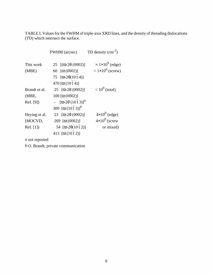
In addition to TEM analysis, the structural quality of our films has been characterizeHRXRD. Table I shows average results for a number of films grown near 750 C, comparthose of other groups. Our results are comparable to those of Brandtet al. [9] who use similar sub-strate preparation and growth methods. Similarly, these MBE results compare favorably wiresults for MOCVD growth on sapphire of Heyinget al. [1]. (Different asymmetric reflectionswere measured by the groups listed in Table I, although the values can be scaled in a mannlowing Fig. 8 of Ref. [18]). Our asymmetricω-2θ width is somewhat greater than that of Heyinet al., but the symmetric and asymmetricω-scan widths are significantly less than theirs and tdensity of screw dislocations determined for our samples is much lower than that for the MOon sapphire growth. Recent theoretical work indicates that edge dislocations may be prefcompared to screw dislocations since, at least for full core dislocations, the latter do have stthe gap whereas the former do not [19].
5 Electrical Characterization
Temperature dependent conductivity and Hall effect measurements have been performed ofilms grown on semi-insulating SiC substrates. For all our films grown with thein situSi-cleaningstep described in Section II we find a relatively high background n-type carrier concentrationically 5 × 1017 cm-3 at room temperature. This value is derived assuming that the carriers areformly distributed throughout the entire GaN film. Typical electron mobilities of about 50 cm2/Vsare observed at room temperature. When the temperature is reduced down to 13 K we find tapparent carrier concentration doesnot decrease significantly (it actually increases slightly)would be expected for carrier freeze-out onto the donor impurities, indicating that the roomperature carrier concentration must be indicative of conductance through a much thinner rThat is, the actual electron concentration must be significantly greater than 1018 cm-3 in order toproduce the degenerate electrical behavior, and thus the thickness of this highly doped layebe less than the total layer thickness.
SIMS measurements have been performed on the GaN films in an effort to identify thesible source of the background donors. Carbon and oxygen concentrations are found to bethe sensitivity of the SIMS, which is 1× 1017 cm-3 and 2× 1017 cm-3 for those elements respectively. Si is consistently observed in the films at a level of around 1× 1018 cm-3, although the Siconcentration varies by about an order of magnitude from film to film and also shows considevariation at different locations within the same film. A typical SIMS profile is shown in Fig. 8Si concentration of about 1.5× 1017cm-3 is found at a point halfway through the film. An appareincrease in Si is seen near the surface, although this could be an artifact due to charging efthe SIMS measurement. Near the SiC/GaN interface a sharp increase in the Si concentrafound. This may indicate a buildup in the Si near the interface, although some uncertainty exthis interpretation since the ions may be sputtering the film nonuniformly (i.e. due to the disloca-tions in the film) resulting in a premature signal from the substrate. In any case, it is clear tsubstantial Si concentration exists in the films, and this can produce the observed n-type
°
5
parede H-m the
ervedave
D-thiseparedaning
inedBE)eenscence,insice sim-
s inbroadset ofd foral-rown
isingfaults
in Fig.hich. Thist im-reby6(b),ar thehich,
Figuresultstionsntense
deep.8 eV
ground carrier concentration.
As discussed above, nearly all the films we have grown and characterized were preusing thein situ Si-cleaning step to remove the surface oxide formed during transfer from thetching apparatus and the MBE system. It is possible that the Si seen in the films arises froexcess 1/3 ML of Si which is left on the surface after this cleaning step; the amount of Si obsin the SIMS profiles is roughly consistent with this mechanism. To test this possibility, we hprepared several filmswithout using the Si-cleaning step, either by overgrowing on MOCVgrown GaN or by growing on sapphire (the latter yielding N-polar material [11]). We find incase background carrier concentrations which are 3–10 times lower than for the samples prwith Si-cleaning, indicating that excess Si in those samples is indeed arising from the Si-cleprocedure.
6 Optical Characterization
A typical low-temperature PL spectrum obtained from our GaN films is shown in Fig. 9, obtafrom a sample grown with Ga/N flux ratio of about 1.6. An intense donor bound exciton (Dline, (D0,X), at 3.47 eV is seen, with FWHM of 10 meV. Donor-acceptor (D-A) features are sin the range 3.1–3.3 eV, and deep luminescence bands are seen near 2.8 eV (blue lumineBL) and 2.2 eV (yellow luminescence, YL). We tentatively associate the 2.8 eV band with intrdefects such as N vacancies, as seen in Mg-containing material [20], although we do note thilarity of this band with one previously reported in GaN films and attributed to D-A transitionthe SiC substrates [21]. The 2.2 eV band is commonly observed in GaN prepared under arange of conditions. A set of weak lines is seen in the range 3.33–3.43 eV, as shown in the inFig. 9. The line at 3.40 eV has been associated with oxygen in GaN [22]. In our case, we finour early films which were grown without a nitrogen purifier (see Section II) that this line wasways observed and it sometimes had a large intensity comparable to the DBE. Later films, gwith the nitrogen filter, show no evidence of this line, thus supporting its interpretation as arfrom oxygen (O). The set of lines centered near 3.35 eV have been associated with stacking(SF) near the GaN/SiC interface [23].
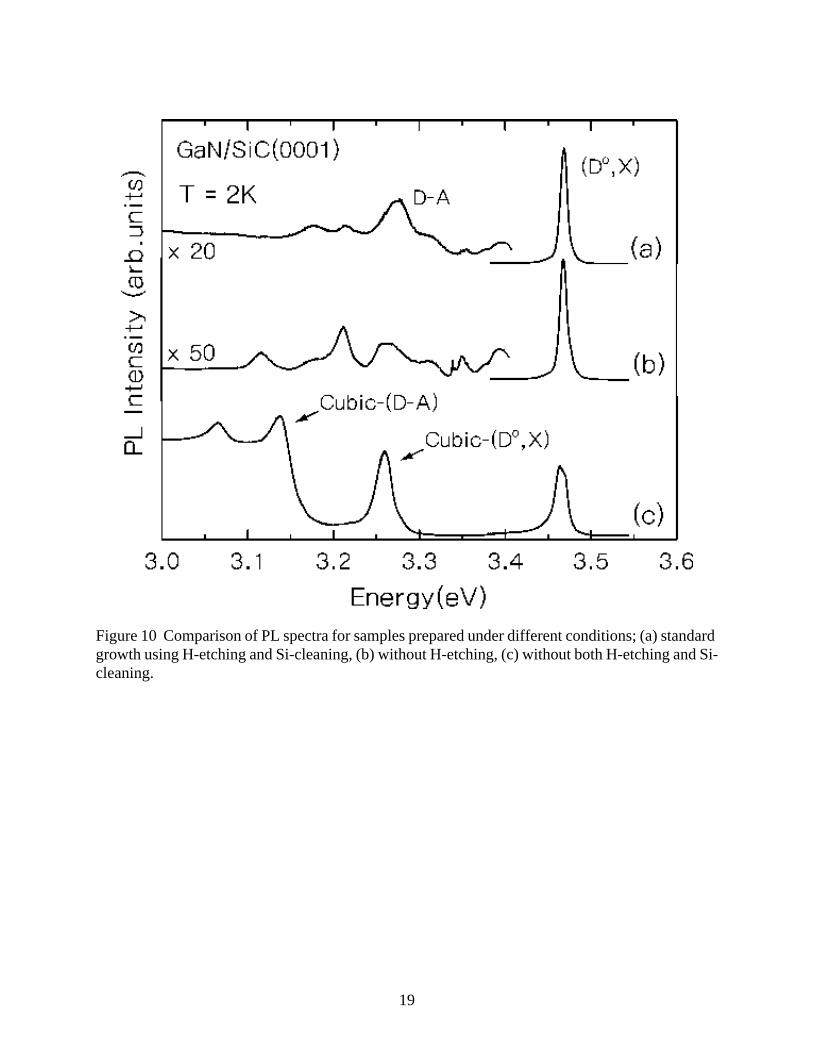
Figure 10 shows the effect of substrate preparation on the spectra. The spectrum10(a) is identical to that of Fig. 9. Figure 10(b) shows a spectrum obtained from a sample for wthe H-etching procedure was not used but the Si-cleaning of the substrate was performedspectrum shows different D-A features than those of our other films, suggestive of a differenpurity concentration in the sample (the H-etching removes the top nm of the SiC, theremoving impurities from the surface as well). As discussed in Section IV and shown in Fig.this sample has numerous stacking faults which define small regions of cubic stacking neGaN/SiC interface. The spectrum in Fig. 10(b) shows a clear set of SF lines near 3.35 eV, wat least compared to the D-A luminescence have greater intensity that those of Fig. 10(a).10(c) shows a spectrum obtained from a film grown without H-etching or Si-cleaning. TEM refrom this sample (not shown) indicated very poor structural quality, with numerous dislocaand stacking faults, and large regions of cubic stacking in the material. The spectrum shows iDBE and D-A pair lines from cubic GaN [24].
Figure 11 shows the influence of the Ga/N flux ratio on the spectra, particularly for theluminescence. We consistently find that as this flux ratio is increased, the BL feature near 2
150∼
6
on ofin-
e seed
arisonfea-
inal-
ns forg ofraturecationn theomen the
was0333,619),
. S.
. K.
tron.
A
ppl.
and
nd
s.
shows greater intensity relative to the 2.2 eV YL. This result is consistent with the expectatiN vacancy formation under very Ga rich conditions. We also note that the width of the DBEcreases with increasing Ga/N ratio, and for the least Ga rich conditions (bottom spectrum) wan indication of a free exciton shoulder,FX
A, at 3.48 eV. The spectra in Fig. 11 were all acquireusing He-Cd excitation. An intense line at 3.448 eV is seen in the spectra, and from compwith similar spectra acquired with frequency-doubled Ar laser excitation we can identify thisture as arising from the He-Cd laser line which is Raman shifted by multiple GaN longitudoptical phonon energies, in agreement with the identification of Dewsnipet al. [25] .
7 Summary
In summary, we find that the use of appropriate substrate preparation and growth conditioGaN on SiC heteroepitaxy can lead to material of relatively high structural quality. H-etchinthe substrate is important to eliminate stacking disorder in the GaN, and high growth tempereduces the density of screw dislocations in particular. The mechanisms underlying the disloformation and annihilation are fairly well understood. A background electron concentration imid-1017 cm-3 range is found in the films, and is tentatively attributed to Si donors arising frthe Si-cleaning step (used to remove surface oxide formed during the sample transfer betweH-etching apparatus and the MBE chamber).
Discussions with O. Brandt and J. S. Speck are gratefully acknowledged. This worksupported in part by the Office of Naval Research (grants N00014-96-1-0214, N00014-96-1-and N00014-99-1-1067), the Air Force Office of Scientific Research (grant F33615-95-C-1and the National Science Foundation (grant DMR-9985898).
[1] B. Heying, X. H. Wu, S. Keller, Y. Li, D. Kapolnek, B. P. Keller, S. P. DenBaars, and JSpeck, Appl. Phys. Lett.68, 643 (1996).
[2] D. Kapolnek, S. Keller, R. Vetury, R. D. Underwood, P. Kozodoy, S. P. DenBaars, and UMishra, Appl. Phys. Lett.71, 1204 (1997).
[3] O.-H. Nam, M. D. Bremer, T. S. Zheleva, and R. F. Davis, Appl. Phys. Lett.71, 2638 (1997).
[4] V. Ramachandran, M. F. Brady, A. R. Smith, R. M. Feenstra, and D. W. Greve, J. ElecMater.27, 308 (1998).
[5] V. Ramachandran, A. R. Smith, R. M. Feenstra, and D. W. Greve, J. Vac. Sci. Technol.17,1289 (1999).
[6] V. M. Torres, J. L. Edwards, B. J. Wilkens, D. J. Smith, R. B. Doak, and I. S. T. Tsong, APhys. Lett.74, 985 (1999).
[7] Q. Z. Xue, Q. K. Xue, Y. Hasegawa, I. S. T. Tsong, and T. Sakurai, Appl. Phys. Lett.74, 2468(1999).
[8] R. Lantier, A. Rizzi, D. Guggi, H. Lüth, B. Neubauer, D. Gerthsen, S. Frabboni, G. Colì,R. Cingolani, MRS Internet J. Nitride Semicond. Res.4S1, G3.50 (1999).
[9] O. Brandt, R. Muralidharan, P. Waltereit, A. Thamm, A. Trampert, H. von Kiedrowski, aK. H. Ploog, Appl. Phys. Lett.75, 4019 (1999).
[10] E. J. Tarsa, B. Heying, X. H. Wu, P. Fini, S. P. DenBaars, and J. S. Speck, J. Appl. Phy82,5472 (1997).
7
. L.emi-
MRS
ve, J.
peck,
ternet
tter,
. H.
ett.
Rev.
B.
[11] A. R. Smith, V. Ramachandran, R. M. Feenstra, D. W. Greve, A. Ptak, T. H. Myers, WSarney, L. Salamanca-Riba, M.-S. Shin, and M. Skowronski, MRS Internet J. Nitride Scond. Res.3, 12 (1998).
[12] V. Ramachandran and R. M. Feenstra, Phys. Rev. Lett.82, 1000 (1999).
[13] C. Youtsey, L. T. Romano, R. J. Molnar, and I. Adesida, Appl. Phys. Lett.74, 3537 (1999).
[14] A. Sagar, C. D. Lee, and R. M. Feenstra, unpublished.
[15] B. W. Dodson and J. Y. Tsao, Appl. Phys. Lett.51, 1325 (1987).
[16] W. L. Sarney, L. Salamanca-Riba, V. Ramachandran, R. M. Feenstra, and D. W. Greve,Internet J. Nitride Semicond. Res.5S1, W3.47 (2000).
[17] V. Ramachandran, R. M. Feenstra, W. L. Sarney, L. Salamanca-Riba, and D. W. GreVac. Sci. Technol. A, Jul/Aug (2000), to appear.
[18] P. Fini, X. Wu, E. J. Tarsa, Y. Golan, V. Srikant, S. Keller, S. P. DenBaars, and J. S. SJpn. J. Appl. Phys.37, 4460 (1998).
[19] J. Elsner, Th. Frauenheim, M. Haugk, R. Gutierrez, R. Jones, and M. E. Heggie, MRS InJ. Nitride Semicond. Res.4S1, G3.29 (1999).
[20] U. Kaufmann, M. Kunzer, M. Maier, H. Obloh, A. Ramakrishnan, B. Santic, and P. SchloAppl. Phys. Lett.72, 1326 (1998).
[21] O. Brandt, B. Yang, H.-J. Wünsche, U. Jahn, J. Ringling, G. Paris, H. T. Grahn, and KPloog, Phys. Rev. B58, R13407 (1998).
[22] J. M. Hayes, M. Kuball, A. Bell, I. Harrison, D. Korakakis, and C. T. Foxon, Appl. Phys. L75, 2097 (1999).
[23] W. Rieger, R. Dimitrov, D. Brunner, E. Rohrer, O. Ambacher, and M. Stutzmann, Phys.B 54, 17596 (1996).
[24] J. Menniger, U. Jahn, O. Brandt, H. Yang, and K. Ploog, Phys. Rev. B53, 1881 (1996).
[25] D. J. Dewsnip, A. V. Andrianov, I. Harrison, D. E. Lacklison, J. W. Orton, J. Morgan, G.Ren, T. S. Cheng, S. E. Hooper, and C. T. Foxon, Semicond. Sci. and Technol.12, 55 (1997).
8
ns
TABLE I. Values for the FWHM of triple-axis XRD lines, and the density of threading dislocatio(TD) which intersect the surface.FWHM (arcsec) TD density (cm-2)
This work 25 [(ω-2θ (0002)] ≈ 1×10⁹ (edge)
(MBE) 60 [ω (0002)] < 1×10⁶ (screw)
75 [ω-2θ(10 4)]
470 [ω (10 4)]
Brandt et al. 25 [ω-2θ (0002)] < 109 (total)
(MBE, 100 [ω (0002)]
Ref. [9]) - [ω-2θ (10 3)]a
300 [ω (10 3)]b
Heying et al. 23 [ω-2θ (0002)] 4×10⁸ (edge)
(MOCVD, 269 [ω (0002)] 4×10⁸ (screw
Ref. [1]) 54 [ω-2θ(10 2)] or mixed)
413 [ω (10 2)]
a not reported
b O. Brandt, private communication
1
1
1
1
1
1
9
ave
Figure 1 AFM image of SiC(0001) surface following the Si-cleaning step. All observed steps ha height of 7.5 Å (the small hexagonal pits are also 7.5 Å deep). Grey-scale range is 15 Å.10
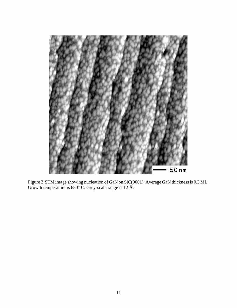
ML.
Figure 2 STM image showing nucleation of GaN on SiC(0001). Average GaN thickness is 0.3Growth temperature is 650 C. Grey-scale range is 12 Å.°11
uxtions.
Figure 3 AFM images of GaN(0001) film grown at 750 C on H-etched 6H-SiC, with Ga/N flratios of (a) 1.3, (b) 1.1, and (c) 1.6. Pits on the surface are seen in (a), arising from dislocaThe grey-scale ranges are 5 nm, 86 nm, and 5 nm for (a)–(c) respectively.
°
12
-
Figure 4 (a) and (b) Dark field two-beam TEM images of GaN films grown on H-etched 6HSiC(0001), (a) g=[01 0] and (b) g=[0002]. Arrows mark the GaN/SiC interface.113
y
Figure 5 SEM image of GaN film, grown at 750 C, which has been photoelectrochemicalletched to reveal the dislocations. The scale bar corresponds to a length of 5µm.°
14
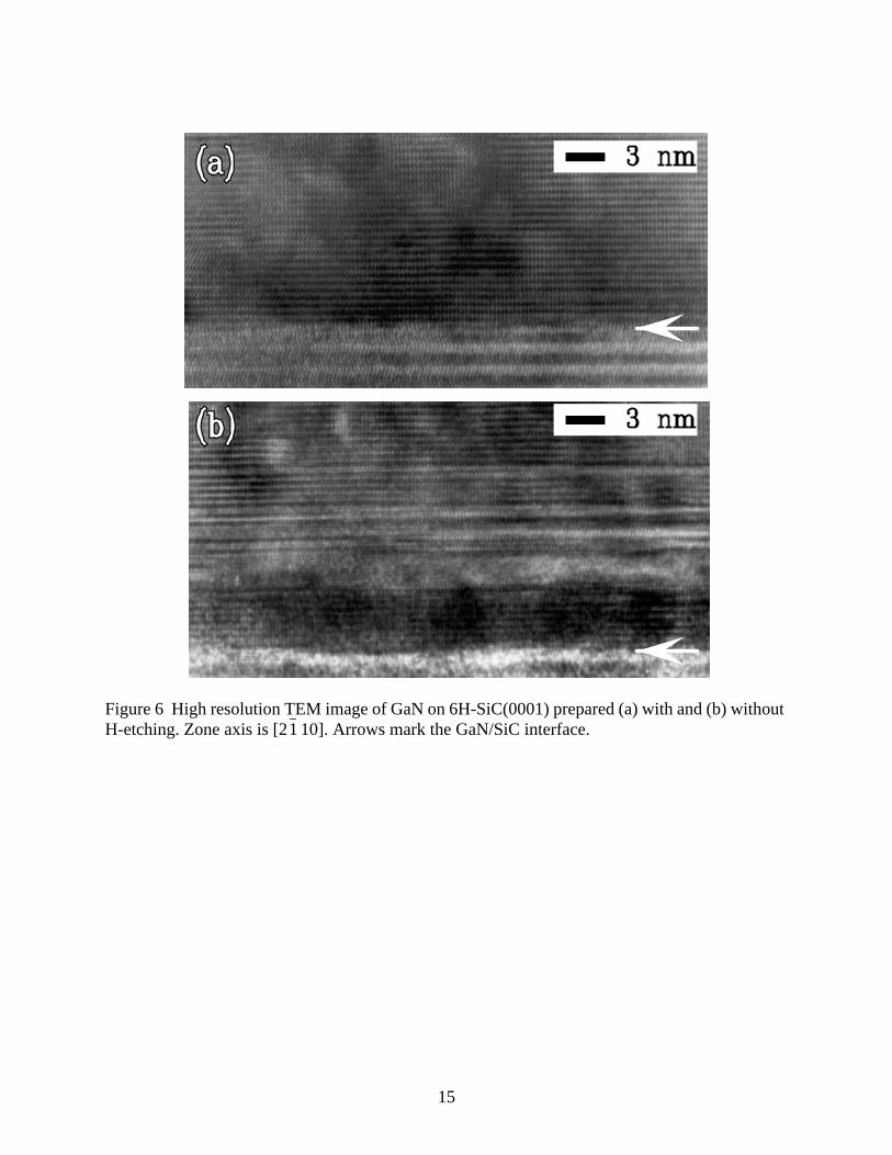
out
Figure 6 High resolution TEM image of GaN on 6H-SiC(0001) prepared (a) with and (b) withH-etching. Zone axis is [2 10]. Arrows mark the GaN/SiC interface.115
le
Figure 7 Stacking sequence for GaN layers on SiC, illustrating the manner in which a singbilayer step in the SiC produces oppositely oriented GaN grains on the two terraces.16
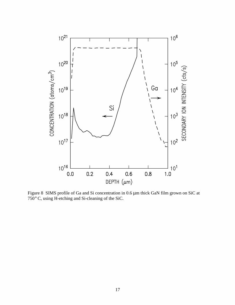
Figure 8 SIMS profile of Ga and Si concentration in 0.6µm thick GaN film grown on SiC at750 C, using H-etching and Si-cleaning of the SiC.°
17
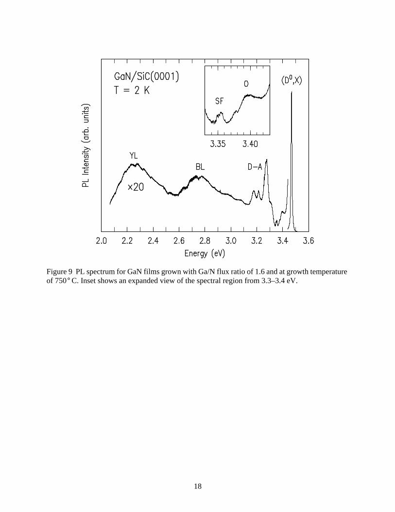
ure
Figure 9 PL spectrum for GaN films grown with Ga/N flux ratio of 1.6 and at growth temperatof 750 C. Inset shows an expanded view of the spectral region from 3.3–3.4 eV.°18
ndardSi-
Figure 10 Comparison of PL spectra for samples prepared under different conditions; (a) stagrowth using H-etching and Si-cleaning, (b) without H-etching, (c) without both H-etching andcleaning.
19
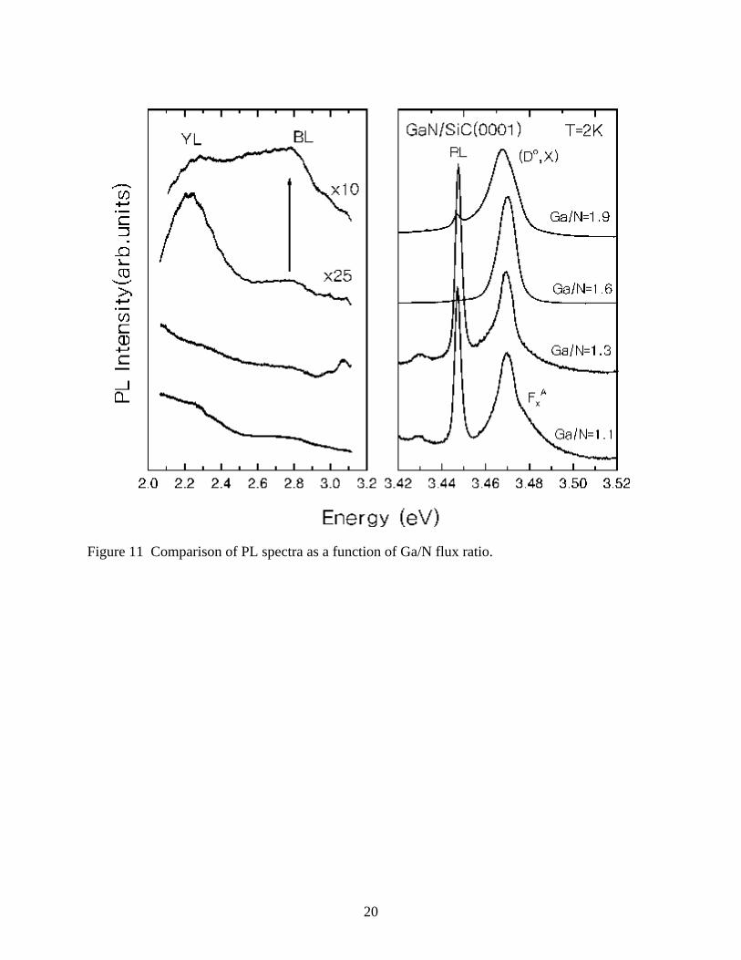
Figure 11 Comparison of PL spectra as a function of Ga/N flux ratio.
20