
Properties and applications of optical thyristors
15
HAL Id: jpa-00249271 https://hal.archives-ouvertes.fr/jpa-00249271 Submitted on 1 Jan 1994 HAL is a multi-disciplinary open access archive for the deposit and dissemination of sci- entific research documents, whether they are pub- lished or not. The documents may come from teaching and research institutions in France or abroad, or from public or private research centers. L’archive ouverte pluridisciplinaire HAL, est destinée au dépôt et à la diffusion de documents scientifiques de niveau recherche, publiés ou non, émanant des établissements d’enseignement et de recherche français ou étrangers, des laboratoires publics ou privés. Properties and applications of optical thyristors Paul Heremans, Maarten Kuijk, Roger Vounckx, Gustaaf Borghs To cite this version: Paul Heremans, Maarten Kuijk, Roger Vounckx, Gustaaf Borghs. Properties and applications of optical thyristors. Journal de Physique III, EDP Sciences, 1994, 4 (12), pp.2391-2404. <10.1051/jp3:1994285>. <jpa-00249271>
Transcript of Properties and applications of optical thyristors

HAL Id: jpa-00249271https://hal.archives-ouvertes.fr/jpa-00249271
Submitted on 1 Jan 1994
HAL is a multi-disciplinary open accessarchive for the deposit and dissemination of sci-entific research documents, whether they are pub-lished or not. The documents may come fromteaching and research institutions in France orabroad, or from public or private research centers.
L’archive ouverte pluridisciplinaire HAL, estdestinée au dépôt et à la diffusion de documentsscientifiques de niveau recherche, publiés ou non,émanant des établissements d’enseignement et derecherche français ou étrangers, des laboratoirespublics ou privés.
Properties and applications of optical thyristorsPaul Heremans, Maarten Kuijk, Roger Vounckx, Gustaaf Borghs
To cite this version:Paul Heremans, Maarten Kuijk, Roger Vounckx, Gustaaf Borghs. Properties and applicationsof optical thyristors. Journal de Physique III, EDP Sciences, 1994, 4 (12), pp.2391-2404.<10.1051/jp3:1994285>. <jpa-00249271>

J. Phj,s. III Franc-e 4 (1994) 2391-2404 DECEMBER 1994, PAGE 2391
Classification
Physics Abstracts
78.90
Properties and applications of optical thyristors
Paul Heremans ('), Maarten Kuijk (~), Roger Vounckx (~) and Gustaaf Borghs (')
(') Interuniversity Micro-Electronics Center (IMEC), Kapeldreef75, 3001Leuven, Belgium(2) Vrije Universiteit Brussel, Applied Physics Dept. (TONA), Pleinlaan2, 1050Brussel,
Belgium
(Received II January 1994, II May 1994)
Abstract. The optical thyristor is a promising device for optical information processing. It
combines a receiving-, transmitting- and memory function in a single device, with at the same time
a considerable optical gain. We show in this paper the dynamics of differential switching, I-e-, the
switching of a single thyristor in an array of thyristors, and compare it to the switching of a singledevice. We also review the recent developments which have led to a dramatic increase of the speed
and optical sensitivity of optical thyristors. Finally, we show some interesting applications which
have been realized with differential switching in arrays of sensitive thyristors (5 x 5, 16 x16 unto
32 x 64 devices), such as locating the maximum light intensity or integrated intensity of opticalinput patterns, and transcription of optical information from one thyristor array to another in free
space.
1. Introduction.
Computing science evolves in the direction of conceiving parallel electronic computing
systems. Unfortunately, the interconnection bottleneck seriously limits the increase of
performance achievable with parallel processing. Massive optical interconnects could solve
this bottleneck. Even more promising can be the realization of certain functions, like
memorization, shifting and logical AND/NAND/OR/NOR done in a parallel optical way,
using arrays of smart pixels.The optical thyristor, usually implemented as a double-heterojunction PnpN structure in the
GaAs/AlAs material system, is a bi-stable optoelectronic switch. The family comprises the
DOES [1, 2], the VSTEP[3], the pnpn optical switch [4], the DHOT[5], and devices
consisting of the vertical integration of an LED (or laser diode) and a heterojunction bipolartransistor, such as the LED-HPT [6], the LD-HPT [7], and the LAOS [8]. In the off-state,these latching devices have a high impedance, while in the on-state, they are conductive and,like an LED, emit light perpendicularly to the surface. Because of their versatility, they are
currently considered to be candidate switches for parallel optoelectronic information transmis-
sion and processing, and memorization. Indeed, they combine the following assets : I) theyswitch from the off-state to the on-state when they receive an optical [I or electrical [2] input ;
§Les Editions de Physique 1994

2392 JOURNAL DE PHYSIQUE III N° 12
2) they are active devices the output light is generated, rather than being derived from the
input light (this property is fundamental for cascaded logic operations in subsequent layers) ;
3) they memorize their on-state 4) smart pixels can be constructed with them for implemen-ting logic functions 5) they are relatively simple to integrate into arrays.
The above-described versatility is a requirement for an optoelectronic switch, but it is not
sufficient. Following parameters are of prime importance for a switch to be competitive Ii the
optical input energy required for switching from the dark off-state to the light-emitting on-
state ; 2) the optoelectronic conversion efficiency which determines the electrical power
necessary for the required fan-out 3) the switch-on speed and the switch-off speed.In the present paper, we give an overview of recent research efforts which have pushed the
optical thyristor towards low energy and high speed. We will also demonstrate some
applications which have to date been realized.
2. The optical thyristor.
Optical thyristor layers are grown by Molecular Beam Epitaxy. The layer sequence is n-p-n-p
or p-n-p-n. A typical device stucture is shown in figure I. Starting from a p-type GaAs wafer, a
I ~m heavily p-doped buffer layer is grown, followed by
P : 500 nm 3 xlo'? cm~~ p-doped (Be) Alo~oGao~oAs, called the P-emitter
n: 60nm n-doped (Sij GaAs called the n-'base (it consists of 10nm doped at
n =
6 x10'~ cm~~ and 50 nm doped at n = x
10'~ cm~~)
p:304nm p-doped (Be) GaAs called the p-base (it consists of 280nm doped at
p =x
lo'? cm~~ and ?0 nm doped at p =
I x10'~ cm~~)
;
N 250 nm 2 xlo'? cm~~ n-doped (Si) AlojoGao~oAs, called the N-emitter, capped by a
140 nm contact layer of n+-doped (Si) GaAs.
contact: 10x50 pnj
window
140 mn GaAs n=6xii ~cni~
250nmAl ~G~ As n=2x1/~cni~
bonding pad20 nm G A~ S cm
280 mn GaAs p- j~ j/7~~3
cm
IO mn GaAs cm
500nmAl G~ As p=3xli~cni~
p+GaAs subswate
Fig. 1. Cross-section of a typical processed PnpN device.

N° 12 PROPERTIES AND APPLICATIONS OF OPTICAL THYRISTORS 2393
The tolerance on the layer thicknesses and doping concentrations is typically 20 fb, such that
basically all devices processed on a 2-inch MBE-grown wafer but those on the outer half cm
satisfy the specifications.Mesas of several sizes (30 ~m x 30 ~m up to loo ~m x
200 ~m) and 1.16 ~m high are
obtained by wet etching in a 3 :1 : 50 solution of H~P04. H~O~ : H~O. Their top (cathode)
contact is a pad of AuGe/NilAu obtained by lift-off, that leaves an optical window over the
remainder of the mesa surface. The quasi static electrical characteristics of such device are
shown in figure 2. Pairs and arrays of such elements are obtained on chip by connecting the
top-contacts in the processing cycle.
pixel 60
'~~
%~°~~Wg cuwcnt
0 2 4 6 8 lo
Anode voltage IV)
Fig. 2. Current-voltage characteristics of the device of figure I. with mesa area of 50x 60 ~m~.
3. Switching principles.
Several switching principles can be used, leading to a different optical input sensitivity, a
different functionality, and a different switching behavior.
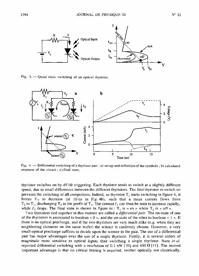
3.I QUASI STATIC SWITCHING. in figure 3, the classical set-up is shown for an opticallyswitched photo-thyristor. This is also the way three-terminal Si-thyristors normally operate.
The thyristor is connected in series with a load and a power supply. The voltage is increased up
to V~. The voltage ramp must be slow~, such as to avoid unwanted triggering of the thyristor to
its on-state a well-known phenomenon known as dV/dt triggering [9]. The thyristor is then
in its off-state, at V~ (smaller than the breakover voltage V~~). When a light pulse, containingsufficient energy, impinges on the device, the breakover voltage lowers, and the device
switches on. If made in III-V, the device emits light in this on-state. In the on-state, the current
I is several orders of magnitude larger than in the off-state, and since the light-output is (to a
first approximation) proportional to this current, a very high on-off contrast ratio can be
obtained (102 10~). The main advantage oi this switching principle is that the operation is
asynchronous. The most important drawback is that for obtaining a high sensitivity for opticalinputs. V, must be chosen very close to V~~, hence the time necessary to increase the voltage
unto V~ without dV/dt triggering is prohibitively long (milliseconds).
3.2 DIFFERENTIAL SWITCHING. One can try to make use of the fast dV/dt triggering to one's
own advantage. To this end, two or more optical thyristors are connected in parallel, with a
common external resistance R~ (Fig. 4a). The supply voltage V~ is ramped fast, such that one
2394 JOURNAL DE PHYSIQUE III N° 12
R I
/ Opfical Input~/ ~"
. ",
~ ~ lh
~ ~Opfical Output ~~~ °~~
V~s ~br
Fig. 3. Quasi static switching of an optical thyristor.
v~ a b
,~~~~---~~--
j j
,-"' ~4
2."
<;"' )
,"2 fj_-."' ~i
0
1 ( ~
~
' winncrfi C I 2
.,'
~0
, i~
V 0 5 10 15
Tirnc ins)
Fig. 4. Differential switching of a thyristor pair : a) set-up and definition of the symbols b) calculated
response of the circuit c) final state.
thyristor switches on by dV/dt triggering. Each thyristor tends to switch at a slightly different
speed, due to small differences between the different thyristors. The first thyristor to switch on
prevents the switching of all competitors. Indeed, as thyristor Tj starts switching in figure 4, it
forces V~ to decrease (at 10ns in Fig. 4b), such that a maze current flows from
T~ to Tj, discharging T~ to the profit of Tj. The current Ii can then be seen to increase rapidly,while I~ drops. The final state is shown in figure 4c Tj is
« on »while T~ is
«off
».
Two thyristors tied together in this manner are called a differential pair. The on-state of one
of the thyristors is associated to boolean«
0 », and the on-state of the other to boolean« ».
If
there is no optical precharge, and if the two thyristors are very much alike (e.g. when they are
neighboring elements on the same wafer) the winner is randomly chosen. However, a very
small optical precharge suffices to decide upon the winner in the pair. The use of a differential
pair has major advantages over the use of a single thyristor. Firstly, it is several orders of
magnitude more sensitive to optical inputs than switching a single thyristor. Hara et al.
reported differential switching with a resolution of 0.I nW [10] and 400 fJ [I I]. The second
important advantage is that no critical biasing is required, neither optically nor electrically.

N° 12 PROPERTIES AND APPLICATIONS OF OPTICAL THYRISTORS 2395
Due to this and to the fact that the switching is induced electrically, there is no critical-slowing-down phenomenon, I.e., no trade-off between switch-on speed and optical sensitivity [I I]. A
third advantage is that the boolean information is transmitted in dual-rail code, I.e., the
thyristor pair emits a signal for the transmission of both a «0
»and a «
I».
This is known to
strongly improve the bit-error rate for the transmission. A draw-back of using a differential pair
is that some type of electrical clocking is needed.
The parallel set-up of more than two thyristors is called a Winner-Takes-All network [12].
Such network can be used to find the maximum light intensity of an input light pattem, as
described further.
4. Improvement of the optical sensitivity by low emitter doping.<
The optical sensitivity of optical thyristors depends on the doping concentrations of the emitter
layers and of the base layers. For small anode currents, the base current of each bipolartransistor of the two-transistor equivalent model of a thyristor [9] is dominantly determined by
the surface recombination current [13] at the perimeter of the mesa within the space chargeregion between each emitter and base. Although the pinning of the Fermi level at the surface
reduces the effective barrier height at the surface, for small emitter-base voltages
V~~ [14] this surface recombination current can still be expressed by the well-known
formula jls]
q V~~(I)Isu~,
rec~
jq~~~~ ~~ ~~~
2 kT
where P is the mesa perimeter, n~ is the intrinsic concentration and AW is the width of that
portion of the space charge region where the maximal recombination occurs smaller than
the complete space charge region [14]. Because of the pinning of the Fermi-level at the
surface, S is an «effective» surface recombination velocity (m lo? cm/s). Equation (I)
assumes the recombination to occur over AW at maximum rate, I-e- at the rate that is reached
when the electron and hole concentrations are equal. This rate is in fact only reached on one
contour line (around the mesa) of the space charge region. Analogously to the reduction of the
bulk recombination in the space charge region [16], it is crucial to position this contour line in
the wide-bandgap material, because ni, and therefore the recombination current, is then much
smaller.
In our devices, 80 to 95 fb of the emitter-base space charge region is located in the (wide
bandgap) emitters, because the emitter doping is 5 to 20 times smaller than the adjacent base
doping. AW is therefore located in the wide bandgap layers, and the surface recombination
currents are thus reduced. To demonstrate the improvement of using such low emitter doping
to increase the optical sensitivity, we measured simple bipolar heterojunction transistors
(HBT). Figure 5 shows the DC amplification p of the photo-generated current of a normal
bipolar Npn transistor (with N~rr~jj~~ =
10'~ cm~ ~ and N~~~~=
2 x10~? cm~ ~), and of an Npn
transistor with lightly doped emitters (with N~rr~jj~~ =
10'? cm~~ and N~~~~ =
10'~ cm~~) for
several optical inputs. An identical current amplification is reached at a 000 times smaller
current level in the case of low emitter doping.As a result of this increase in gain of the two transistors inside the thyristor, our optical
thyristors have a low holding current (0.2 to 2 ~A), the lowest reported for thyristors with no
mesa-passivation. The improved gain at low current levels thus obtained makes these thyristors
more sensitive to input light. This method of dealing with the surface recombination has the
obvious advantage that the performance of the thyristors does not degrade with time, which is a
concem when mesa-passivation techniques [17, 18] with dubious long-term stability are used.

2396 JOURNAL DE PHYSIQUE III N° 12
N~~~~~~ =10~] N~~~=10~~cm'~
~
e~
~N~~~~~~ =10~i N~~~~ =2 x10~~ cm~~
lo~
lo~
lo~
lo-~
lo"
Cuwcnt(A)
Fig. 5. Measured gain (= collector current/photo-generated current) of two Npn transistors i,eisus the
collector current. To obtain the same gain p, a three orders of magnitude smaller current is needed when
the emitter is doped significantly less than the base.
The improvement in the optical sensitivity obtained with this technique allows cascadable
optical switching. This means that a thyristor can be switched on by illuminating it with the
light of a similar device. In figure 6, the current characteristics of a thyristor are shown for
several values of the incident optical power gene;ated by an identical thyristor. It is clear that a
thyristor can easily be switched when illuminated by a twin device.
s
io~
~i
)10
~2.20 pW
~~
1.76 pw
lo~
~~
0.52 pw
o~~
2 3 4 5
Voltage IV)
Fig. 6. Current-voltage characteristics of a thynstor (with 110 x 55 ~m~mesa and 100 x 35 ~m~
window) at several optical inputs generated byaft
identical thyristoi

N° 12 PROPERTIES AND APPLICATIONS OF OPTICAL THYRISTORS 2397
~~ ~Pn~a
V~__-~
p
""~~ "~ ---0
n ~/ V~q+
+P N
v~
~~/+v
~
c
j +
Pnp °
v_
d
Fig. 7. Majority carrier extraction from a thyristor by means of a negative anode-to-cathode voltagepulse a) electron extraction from the n-base b) reach-through ; c) hole extraction from the p-based) quasi-steady-state.
5. Depletion of the base layers for improvement of speed and optical sensitivity.
Thyristors are ill-reputed for having a slow turn-off speed [9]. The origin of the turn-off
problem is as follows. In its on-state, a PnpN structure has three forward-biased junctions.When the bias is pulsed to zero, the sum of the biases over the P-n, the n-p and the p-N
junctions is forced to zero, but not the individual values of these biases. The equilibrium state,
with three zero-biased junctions, is reached by self-discharge of the junctions, which is a very
slow process (typically milliseconds). As long as equilibrium is not established, the two center
thyristor layers (n and pi contain more majority carriers than at equilibrium and as a
consequence, the thyristor suffers from enhanced dV/dt triggering. In a single thyristor switch,
this means that the voltage V~ has to be applied even slower than when starting from
equilibrium. In a differential pair, it means that when the voltage is applied, the thyristor which
was in the on-state during the previous cycle will switch on again, even if the light input is
given to his neighbor. To avoid this, the light input, which generates carriers in the thyristorwhich is chosen to switch on, must be increased dramatically (such that the optically generatedcarriers in the intended winner can exceed the left-over carriers in the previous winner). The
trade-off between cycle speed and optical sensitivity is therefore very poor.
To avoid this poor trade-off, the excess majority carriers of the center regions must be
extractid before the light input is given. This has been tried by means of a third and fourth
contact to the center thyristor layers [2, 19-21]. The processing technology then becomes
JOURNAL DE PHYSIQUE III T 4, N'12 DECEMBER 1994

2398 JOURNAL DE PHYSIQUE III N° 12
complex, and the presence of a third and fourth terminal jeopardizes the integration of such
switches in arrays. An easier solution would be extract the carriers by applying a negativeanode-to-cathode voltage pulse. When applying a negative anode voltage V~, as shown in
figure 7a, electrons from the center n-region are extracted faster than holes from the p-region,because the Npn transistor has the better gain. As only few of the slowly-diffusing holes are
evacuated, the majority carrier charge that forward-biases the emitter-base junction of the
better transistor when a positive anode voltage is applied is not much decreased, and this
transistor still rapidly induces dV/dt switching. For this reason, attempts to use a negativevoltage pulse to speed up the turn-off process have not been successful in the past [19].
Recently, a method has been proposed to overcome the above-described problem [5, 22]. It
requires a PnpN device in which the n-type base layer can be completely depleted by reverse
biasing the P-n junction, before this junction breaks down. For a negative anode voltage in
excess of that necessary for the P-n and n-p space charge regions to meet each other through the
n-layer (the«
reach-through»
condition, Fig. 7b), the thermionic emission current of holes
from the p-layer increases dramatically, as the barrier ~P~ against hole emission is decreased
(Fig. 7c). The time constant for the hole extraction is in practice RC -limited (R is the external
resistance) and typically less than lo ns [5]. In the final state (Fig. 7d), the amount of holes in
the p-region can be sufficiently small for dV/dt triggering to be suppressed when the thyristoris switched to the on-state again.
8
V volugePCgVneg~
6laser purge
~- current~
~4
~£~ ++
~ ~+
pixel 60x 50 pm
~-12 -8 -4 0
vncg (v)
Fig. 8. Tum-off characteristics for 30-ns turn-off pulses (v~~~).
The thyristor described in section 2 complies with the requirement that the n-layer can be
depleted completely. The hole-extraction measurement is shown in figure 8. The turn-off was
measured with the voltage pulse cycle (applied over loon) shown in the insert. After a
negative pulse to V~~~ for 30 ns, the voltage is increased in Ions to a certain positive value
V~~~. The thyristor (kept at V~~~) is then switched on by illumination with 670-nm laser light.Then, the voltage is decreased in lo ns to V~~~ again. For each value of V~~~, there is a critical
V~~~ beyond which the thyristor does not switch on when the voltage is pulsed to
V~~~. The current through the thyristor then only flows after triggering by the laser. The relation
between each chosenV~~~ and the corresponding critical V~~~ is shown in figure 8. There is a

N° 12 PROPERTIES AND APPLICATIONS OF OPTICAL THYRISTORS 2399
~_
8 jneg "~9.6 ~
V~~~ =0 V
~c 6 ~~~
~ tn~g =30 ns
~ ~~~i
.,.=., ',j
l~ "" 'j11
~_
,l
l lo 100 1000
Light pulse duration (~s)
Fig. 9. Optical energy for cascaded operation of a differential pair in which the carriers are extracted
between the cycles, as compared to the case when no carrier extraction occurs.
rise of V~~~ for V~~~ in excess of the voltage necessary for punch-through of the n-layer
(- 8 V ). For sufficient V~~~ (- 12 V), the thyristor can abruptly be switched to a reasonably
high voltage (6 V) before dV/dt triggering occurs. This shows that hole extraction from the
center layer has been realized.
When such thyristors are tied in a differential pair, fast and sensitive cascadable operation is
expected. Consider a differential pair of thyristors, one of which is in the on-state. The bias
over the pair is pulsed (over loon) for 30 ns to V~~~ =
9.6 V, then brought to zero. An
optical input, originating from another thyristor, then impinges on a random thyristor of the
pair. Figure 9 shows the relation between the minimum duration and the power of this opticalinput for the correct thyristor of the pair to switch on when a bias V~~~ =
5.6 V is applied to the
pair after the illumination. Depending on the exact history of the switching cycles, 4.6 to
loo pJ are shown to be required. This is to be compared to two extreme cases if the 30-ns
1',=-
l----O f
,,'~<'
d' ',._
'«'
','
I ~''P ' '£ ~
,'
~
"
_,ii
j4, j.
'
~( 4
71~' ("''
a) hi
Fig, lo. Top view of a monolithic 16 x 16 thyristor array, with total area of 775 x 900 ~m~ a) a
distributed 2-dimensional input light pattem is applied to the array b) after the voltage is switched on,
competition leads to a fast and correct switch-on of the thyristor located at the maximum input lightintensity. The winning pixel emits light.

2400 JOURNAL DE PHYSIQUE III N° 12
tum-off pulse does not go negative but remains at 0 V, the minimum duration of the opticalinput pulse is 500 ~s, and the minimum optical energy is more than I nJ ; if, on the other hand,
both thyristors of the pair are in equilibrium (0 V) before the input pulse is applied to one of
them, 4.6 pJ is necessary for correct switching.In the above example, the absorption efficiency of the input light is only about 0.2 fb,
because of the fact that the light is generated by an identical thyristor as the receiving device. If
input light with a shorter wavelength is used, the absorption can be increased easily to 20 fl.
The input light energy then also decreases by two orders of magnitude, I-e-, it becomes 0.05 to
I pJ.A further dramatic reduction of the optical input energy is expected when thyristors are
developed in which both the center n-layer and the center p-layer can be totally depleted [23].Recent results with such thyristors have shown operation with femtojoule optical inputs at tens
of MHz [24].A final comment should be made concerning the electrical energy consumption correspond-
ing to the above-discussed optical energy. The electrical energy dissipated by an LED or a
thyristor generating the light intended to switch on another thyristor is about two orders of
magnitude larger than the optical energy required for correct switching. With the most recent
technological developments, we can estimate the external quantum efficiency of the light-emitter to be 30 fl [25], and the power transmission of the optics to be at best lo fb (using an
optical system with a numerical aperture of 0.6 or better). Also, the active device onlydissipates a fraction (typically 30fl) of the total electrical power, the remainder being
consumed in termination resistances. Hence, 0. I pJ optical energy could correspond to lo pJelectrical energy. This is very attractive when compared to the electrical energy required today
for the transmission of one bit with an electrical interconnect, which is of the order of 250 pJ.
6. Applications.
6. I MAXIMUM INTENSITY LOCALtzATION. In several domains of optical parallel processing,like optical neural nets and pattem recognition, there is a need to identify the location of the
maximum light intensity in a 2D spatially distributed light pattem. A monolithic array of 256
optical thyristors (16 x16) connected in parallel can achieve this [26], using the Winner-
Takes-All principle. Figure 10a shows a photograph of a 16 x 16 thyristor array, on which a
distributed input light pattern is applied ; the result after application of a 6 V step in 20 ns is
shown in figure lob- The thyristor located at the place of the highest intensity has switched on,
and emits tens of ~watts of light. The time span between the start of the voltage step and the
end of the decision is 150 ns.
Instead of a permanent input light pattern, one can also apply an image during a certain time
before applying the voltage. Figure Ii shows the measured differential resolution of the
system. Two random pixels of the array of figure lo, called pixel A and pixel B, each receive
an optical input pulse. Immediately after the optical input, the voltage step is aplied. For all
cases that pixel A receives an optical surplus of at least 80 pJ, only pixel A switches on. The
same holds for pixel B. With smaller differences, the correct decision is not always made
sometimes, even both pixels switch on. Without light input a random pixel of the array wins,
showing that all pixels are identical. Because of its inherent speed, this way of locating the
maximum intensity in a plane can be useful in 4-f processing (this function is usually
accomplished by a CCD-camera in combination with a personal computer), and for symbolicsubstitution.
6.2 MAXIMUM DosE LocALizATioN. In the previous paragraph, an optical image is
exposed on an array of thyristors connected in parallel at 0 V. Then a voltage step is applied,

N° 12 PROPERTIES AND APPLICATIONS OF OPTICAL THYRISTORS 2401
jzj*~~~W
1.6 OOOOOOOOOO((OOOOOOOAOOOOOOOOOOOOOOOOOOAO
~~ OOOOOOAOO
OOOOOAOOO
~l.2
~
~~~~~~~~"-'go~jH OOOOOOOOOOOOOAOOOOOO"- j"~~
~~OOOOOOOOOOOOAOOOOOOO
) OOOOOOOOOOOAOOOOOOOO
'S OOOOOOOOOOAOOOOOOOOOf 0.8 OOOOOOOOOAOOOOOOOOOO
_e OOOOOOOOAOOOOOOOOOOO
fl ~~OOOOOOOAOOOOOOOOOOOO
) ~~~ ~~~~WinningPixd:
o_4 o coo a~~~ O PixdA
oooAoooo O PixdB
~~o oaoooo o A A&B(70%),orAorB
O ADO COO O 11 Randompixeloutof256AOOOOOOO~~~~~~~~~~~~
0.0
O-O 0.2 0.4 0.6 0.8 1-O 1.2 IA 1.6
Optical input pixel B (no
Fig. ii. Optical energy incident on a pixel hversus optical energy on pixel B ; the difference in
optical energy must at least be 80 pi for correct switching, otherwise it is possible that both pixels switch
on.
io'7
O
~~-8Q
B Ofl_9
5i~~
O'I° ~o-10
~O
o O O O ° ~
j~~iiioi io2 io3 io4 ios
Delay (~s)
Fig. 12. The minimum optical energy necessary to reliably switch the illuminated pixel as a function
of the time delay between this optical pulse and the application of the voltage step.
and a winner pops up. In order to demonstrate optical dose integration, similar experiments
were made [26] with a variable time delay between the optical input and the application of the
voltage step. One would expect that the optically induced precharge would leak away duringsuch a delay time, so that the required minimum optical energy with delay would be larger.Indeed, for delays longer than I ms, much larger optical pulses are needed (Fig. 12). However,for delay times smaller than I ms, the minimum optical input energy varies slowly (between 40
and 70 pJ).

2402 JOURNAL DE PHYSIQUE III N° 12
,, , ,
mirror
F/D=0.85
,,
bewn ,,,'
,
,
,', ,
camera ", /
,
,
~, , ,
,
,, ,,
thyristor or
thyristor
wafer
Fig. 13. Set-up used to obtain a mirrored image from one thyristor or thyristor array on another. The
beam splitter is for obtaining an image on the CCD camera.
This means that, to a first approximation, all optical energy incident on the pixel within I ms
before the application of the voltage step is integrated. This is true for all pixels of the array, so
that the maximum optical dose can be localized. For arrays where no care was taken to avoid
surface recombination using the low emitter doping described in section 4, maximum
localization is not possible, because the integration time is too small.
6. 3 ARRAY To ARRAY TRANSCRIPTION OF oPTicAL INFORMATION. We show the possibility
to transcribe optical information from one array to another [27]. The set-up of figure 3 is used
to image each pixel of one array onto the corresponding pixel of another array on the same
wafer. We use monolithic arrays of 5 x 5 elements, in which every thyristor has an own
resistance of about 7 n. Due to this relatively large resistance, the thyristors are less tightly tied
together than in a normal winner-takes-all array. As a result, the competition between the
pixels, which determines the winner, can be attenuated, and this permits to force more than a
single thyristor of the array to switch to its on-state. When a voltage step to 16 V in 20 ns over
loo n common resistance is applied to the array, up to 4 pixels of the 25 can be switched on.
The on-state of these four optical thyristors of the left away can then be transferred to the
neighboring array by applying an analogous voltage step on the receiving array. Figure14
shows the result of the image transcription. [
7. Conclusions.
We have demonstrated that optical thyristors are promising optoelectronic switches. They can
be engineered for fast operation and high optical sensitivity. Operation with lo femtojoule
optical inputs at loo MHz can reasonably be expected to be demonstrated in the near future.
Cascadable operation has been demonstrated, as well as fan-out. Therefore, the switches are
not only promising for optical information transmission, but also for optical processing.
Furthermore, arrays of specially conceived thyristors show interesting functionalities, such as
localization of the maximum intensity and dose of an input pattem or image, and the possibility
to transcribe optical information from array to array.
Further research is oriented towards reducing the required optical energy, increasing the
speed, and improving the cascadability. Attention is also paid to the fabrication of smart pixels
with thyristors.

N° 12 PROPERTIES AND APPLICATIONS OF OPTICAL THYRISTORS 2403
Fig. 14. Photograph of two neighboring arrays. The right array has copied mirrored information (four
pixels) from the left array with the dv/dt triggering scheme.
Acknowledgments.
M. Kuijk acknowledges the Belgian National Fund for Scientific Research for his post-
doctoral fellowship.
References
Iii Taylor G. W., Simmons J. G., Cho A. Y. and Mand R. S., A new double heterostructure
optoelectronic switching device using molecular beam epitaxy, J. Appl. Phys. 59 (1986) 596.
[2] Taylor G. W., Mand R. S., Simmons J. G, and Cho A. Y., Ledistor a three-terminal double
heterojunction optoelectronic switch, Appl. Phys. Left. So (1987j 338.
[3] Ogura I., Tashiro Y., Kawai S., Yamada K., Sugimoto M., Kubota K., Kasahara K., Reconfigura-ble optical interconnection using a two-dimensional vertical to surface transmission electropho-tonic device array, Appl. Phys. Lett. 57 (1990) 540.
[4] Pankove J. I., Hayes R., Mayerfield A., Hanna M., Oh E. G., Szmyd D. M., Suda D., Asher S.,
Matson R., Arent D. J., Borghs G., Harvey M. G., A pnpn optical switch, SPIE 963 OpticalComputing 88 (1988) 191.
[5] Heremans P., Kuijk M., Borghs G., Suda D., Hayes R., Vounckx R., Fast tum-off of two-terminal
double-heterojunction optical thyristors, Appl. Phys. Left. 61 (1992) 1326.
[6] Matsuda K., Takimoto K., Lee D.-H., Shibata J.. Integration of 024 InGaAs/lnP optoelectronicbistable switches, IEEE Trans. Electron Dei,ices 37 (1990) 1630.
[7] Noda S., Takayama T., Shibata K., Sasaki A., High gain and very sensitive photonic switchingdevice by integration of heterojunction phototransistor and laser diode, IEEE Trans. Electron
Devices 39 (1992) 305.
[8] Feld S. A., Beyette F. R., Hafich M. J., Lee H. Y., Robinson G. Y., Wilmsen C. W., Electrical and
optical feedback in an InGaAs/lnP light-amplifying switch, IEEE Trans. Electron Device 38
(1991) 2452.
19] Sze S. M., Physics of Semiconductor Devices, Chapter 4 (Wiley, 1981).II 0] Hara K., Kojima K., Mitsunaga K, and Kyuma K., Differential optical switching at subnanowatt
input power, IEEE Phot. Tech. Lett. 1(1989) 370.

2404 JOURNAL DE PHYSIQUE III N° 12
[11] Hara K., Kojima K., Mitsunaga K., Kyuma K., AlGaAs/GaAs pnpn differential optical switch
operable with 400 fJ optical input energy, Appl. Phys. Left. 57 (1990) 1075.
[12] Pankove J., Radehaus C.. Wagner K., Winner Take All Neural Net, with Memory, Electr. Lent. 26
(1990) 349.
[13] Kuijk M., Vounckx R., Pereira R., Mertens R. P. and BorghsG., Scaling down the double
heterojunction NpnP optoelectronic switching device, Conference on Lasers and Electro-
Optics (CLEO), Anaheim, Ca (1989j.[14] Dodd P. E., Stellwag T. B., Melloch M. R., Lundstrom M.S., Surface and perimeter
recombination in GaAs diodes : an experimental and theoretical investigation, IEEE Trans.
Electron Dei~ices 38 (1991) 1253.
[15] Grove A. S., Physics and Technology of Semiconductor Devices, Chapters 5 and 10 (Wiley, 1967).
[16] Tiwari S. and Frank D. J., Analysis of the operation of GaAlAs/GaAs HBT'S, IEEE Trans.
Etectron Devices 36 (1989) 2105.
[17] Sandroff C. J.. Nottenburg R. N.. Bischoff J. C. and Bhat R., Dramatic enhancement in gain of a
GaAs/AlGaAs heterostructure bipolar transistor by surface chemical passivation, Appt. Phys.Lent. 51 (1987) 33.
[18] Kuijk M., Heremans P. and Borghs G., High sensitive NpnP optoelectronic switch by AlAs
regrowth. Appt. Phys. Lett. 59 (19911 497.
[19] Tashiro Y., Kasahara K., Hamao N., Sugimoto M. and YanaseT., High speed response in
optoelectronic gated thyristor, Jpn J. Appl. Phys. 26 (1987) L1014.
[20] Crawford D. L., Taylor G. W., Simmons J. G., Optoelectronic transient response of an n-channel
double heterostructure optoelectronic switch, Appl. Phys. Lett. 52 (1988) 863.
[21] Kasahara K., Tashiro Y., Hamao N., Sugimoto M., Yanase T., Double heterostructure optoelectro-nic switch as a dynamic memory with low power consumption, Appl. Phys. Lent. 52 (1988 ) 679.
[22] Heremans P., Kuijk M., VounckxR., Borghs G., Fast and sensitive two-terminal double-
heterojunction optical thyristors, Microelectron. Eng. 19 (1992) 49.
[23] Kuijk M., Heremans P.. Vounckx R., Borghs G., The depleted optical thyristor, Appl. Phys. Left.
64 (1994) 2073.
[24] HeremansP., Kuij M., Vounckx R., BorghsG., Differential Optical PnpN switch operating at
16 MHz with 250 fJ optical input energy, Appl. Phys. Left. 65 (1994) 19.
j25] Schnitzer1., Yablonovitch E., Caneau C.. Gmitter T.. SchererA., 30fl external quantum
efficiency from surface textured thin-film light-emitting diodes, Appl. Phys. Lett. 63 (1993j
2174.
j26] Kuijk M., Heremans P., VounckxR., Borghs G., Maximum Optical Dose Detection with a
16 x 16 Monolithic Thyristor Array, IEEE Phot. Techn. Lent. 4 (1992) 399.
[27] Heremans P., Kuijk M., Borghs G., Image transcription between arrays of N-p-n-P optoelectronicsswitches. IEEE Trans. Electron Devices 39 (1992) 2248.