Project report on gsm based borewell water level monitor
48
CHAPTER 1: INTRODUCTION 1.1 INTRODUCTION OF THE SYSTEM In a Farming Field area, there is a need of proper water supply to prevent it from drying and avoiding the over flow condition. If the water level in a Borewell connected near to the field drops below the threshold level for irrigation and Field starts drying and also its pump motor may get air-locked or even burn out due to dry running. It is inconvenient for farmers to walk all the way to their fields at night just to switch the pump motor ‘off.’ Besides, he may never get to know the problem. This problem can be solved by using this GSM-based system that will automatically give the user a call on his mobile phone when the water level in the Borewell drops below or rises to the threshold level for pumping. The user can also remotely ‘switch on’ or ‘switch off’ the pump motor by sending a sms from mobile phone. 1
-
Upload
tarun-arora -
Category
Education
-
view
7.343 -
download
23
description
PROJECT REPORT If the water level in a borewell drops below the threshold level for pumping, its pump motor may get air-locked or even burn out due to dry running. It is inconvenient for farmers to walk all the way to their fields at night just to switch the pump motor ‘off.’ Besides, he may never get to know the problem This problem can be solved by using this GSM-based system that will automatically give the user a call on his mobile phone when the water level in the borewell drops below or rises to the threshold level for pumping. The user can also remotely switch on or switch off the pump motor by sending an SMS from his mobile phone. The system is simple, reliable, portable and affordable.
Transcript of Project report on gsm based borewell water level monitor
CHAPTER 1: INTRODUCTION
1.1 INTRODUCTION OF THE SYSTEM
In a Farming Field area, there is a need of proper water supply to prevent it from drying
and avoiding the over flow condition. If the water level in a Borewell connected near to
the field drops below the threshold level for irrigation and Field starts drying and also its
pump motor may get air-locked or even burn out due to dry running. It is inconvenient
for farmers to walk all the way to their fields at night just to switch the pump motor ‘off.’
Besides, he may never get to know the problem. This problem can be solved by using this
GSM-based system that will automatically give the user a call on his mobile phone when
the water level in the Borewell drops below or rises to the threshold level for pumping.
The user can also remotely ‘switch on’ or ‘switch off’ the pump motor by sending a sms
from mobile phone.
1

CHAPTER 2: BLOCK DIAGRAM
2.1 BLOCK DIAGRAM OF THE SYSTEM
FIG2.1(Block Diagram of GSM based Field Borewell Water Level Monitor)
2

2.2BLOCK DIAGRAM DESCRIPTION
The block diagram consists of a power supply of 220V ac that is stepped down using a
step down transformer. There are two sensors A and B that are inserted into the Borewell
for monitoring the levels of the Borewell. Transistor T1 is used as a sensor driver, and T2
is used as a relay driver. Relay driver drives the relay, that turns the motor ‘on’ or ‘off’.
AT89C51 microcontroller is used in which hex code of the software program written in
‘c’ language and compiled by using Keil software is burnt.
GSM modem(SIM300 v7.03) is global system for mobile communication that works on
the RS-232 standard and MAX-232 is used for generating the signals. The corresponding
output is obtained by MAX232 that generates signals for the GSM modem that in turn
sends signals to the mobile phone of the farmer, also it receives the signals to turn ‘off’ or
‘on’ the motor.
3

CHAPTER 3: CIRCUIT DIAGRAM
3.1CIRCUIT DIAGRAM OF THE SYSTEM
FIG3.1(Circuit Diagram of GSM based Field Borewell Water Level Monitor)
4
3.2 DESCRIPTION
The Circuit comprises the power supply section, water-level sensor circuit,
microcontroller, MAX232 driver, relay driver and GSM modem. The GSM board has a
valid SIM card with sufficient recharge amount to make outgoing calls. The circuit is
powered by regulated 5V DC. The 220V, 50Hz AC mains is stepped down by
transformer X1 to deliver a secondary output of 12V, 250 mA. The transformer output is
rectified by bridge rectifier BR1, filtered by capacitor C1 and regulated by IC 7805 (IC3).
Capacitor C2 bypasses ripples from the regulated supply. LED1 acts as the power-‘on’
indicator. Resistor R1 limits the current through LED1.
The AT89C51 microcontroller is connected to the water-level sensor circuit, relay driver
and MAX232. The microcontroller is programmed to take necessary actions. The mobile
number used in the GSM modem is included in the code before burning the code into the
microcontroller .The water-level sensor circuit comprises transistor T1 (BC548) as sensor
driver and water sensors A and B dipped into the Borewell along with the pipe. Sensor A
is dipped to the threshold point for pumping and sensor B is dipped below the pipe to the
bottom of the Borewell. When water in the Borewell fills to the threshold level, it is
sensed by sensor A and you get a call on your mobile phone. Now you can turn the motor
‘on’ by sending the SMS “motor11 on” from your mobile phone to the SIM number in
the GSM modem. You can also turn the motor ‘off’ by sending the SMS “motor11 off”.
Sensor A is connected to the base of transistor T1 (BC548). When there is a high voltage
at the base, T1 conducts and a low voltage is available at its collector. This low signal is
fed to pin 12 (port pin p3.2) of the MCU.
Similarly, for a low voltage input at the base, T1 stops conducting and a high voltage
signal is available at its collector. So pin 12 of the MCU gets a high signal input. The
high or low Voltage signal at pin 12 is monitored and processed by the program in the
MCU, and decision to turn the motor ‘off’ taken when the water level dips below sensor
A. Pin 3 (port pin p1.2) of the MCU is the output pin. It is connected to relay-driver
5

transistor T2 (BC548) and LED2. T2 drives relay RL1, which, in turn, activates the
motor. LED 2 glows to indicate the motor-‘on’ status.When water level in the Borewell
dips below sensor A, the conducting path between sensors A and B breaks. Hence a
signal is received by the microcontroller. The microcontroller turns the running motor
‘off’ and makes a call to the user’s cell phone through a GSM modem to indicate that the
water level is too low to pump the water and the motor has been switched off. In this
way, the motor is protected from airlocks and burnouts due to dry running. The status of
motor, water level and LED2 are shown in Table(3.1) .
Motor, Mobile and LED Status for Different Water Levels
GBOREWELL WATER LEVEL
MOTOR MOBILE LED 2 REMARKS
FULL ABOVE
POINT A
ON CALL FROM MODEM
ON SMS
OPERATION
TO TURN
OFF MOTOR
EMPTY BELOW
POINT A
OFF CALL
FROM
MODEM
OFF SMS
OPERATION
NOT
ALLOWED
TABLE3.1(Motor, Mobile and LED Status for Different Water Levels)
The GSM modem used in this project is SIM300 V7.03. The GSM module is a
specialized type of modem which accepts a SIM card and operates on a subscriber’s
mobile number over a network, just like a cellular phone. Basically, it is a cell phone
without display. Modem SIM300 is a triband GSM/GPRS engine that works on EGSM
900MHz, DCS 1800MHz and PCS 1900MHz frequencies. GSM modem is RS232-logic-
level compatible, i.e., it takes -3V to -15V as logic ‘high’ and +3V to +15V as logic
‘low’. MAX 232 is used to convert TTL into RS232 logic level and vice versa. Hence
MAX232 is a voltage-level converter used between the microcontroller and the GSM
board. The signal at pin 11 of the microcontroller is sent to the GSM modem through pin
11 of MAX232. This signal is received at Pin 2 (RX) of the GSM.
6

CHAPTER 4: PCB LAYOUT
4.1PCB LAYOUT
FIG4.1(PCB Layout of GSM based Field Borewell Water Level Monitor )
4.2COMPONENT LAYOUT
7

FIG4.2(PCB Layout of GSM based Field Borewell Water Level Monitor )
CHAPTER 5: COMPONENTS DESCRIPTION
5.1CAPACITOR
A capacitor is an electrical device that can store energy in the electric field between a pair
of closely spaced conductors (called 'plates'). When voltage is applied to the capacitor,
electric charges of equal magnitude, but opposite polarity, build up on each plate.
Capacitors are used in electrical circuits as energy-storage devices. They can also be used
to differentiate between high-frequency and low-frequency signals and this makes them
useful in electronic filters. Capacitors are occasionally referred to as condensers. This is
now considered an antiquated term.
8

FIG5.1(Capacitors)
The capacitor's capacitance (C ) is a measure of the amount of charge (Q ) stored on each
plate for a given potential difference or voltage (V) which appears between the plates:
C=Q/V
The capacitance is proportional to the surface area of the conducting plate and inversely
proportional to the distance between the plates. It is also proportional to the permittivity
of the dielectric (that is, non-conducting) substance that separates the plates.
5.2RESISTOR
Electrons move easily through some materials than others when a voltage is applied.
Opposition to current is called resistance.
Numerically, resistance can be defined as the ratio of the potential difference (V) across
its ends to the current (I) flowing through its terminals.
A resistor is a two terminal electronic component that produces a voltage across its
terminals that is proportional to the electric current through it in accordance with Ohm’s
law: R=V/I
9

FIG5.2.1(Voltage-Current relationship of conductor or resistor)
Resistance of a conductor depends on its material, length and area of cross section.
A conductor has low resistance. Short and thin wires have less resistance than long and
thick . The S.I. unit of resistance is ohm.
Resistances are of two types i.e. variable resistor
and fixed value resistors.
Basically, the value of variable resistor stated on
its body but if you want to know the value of
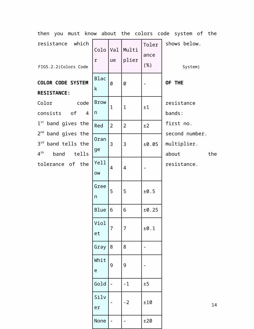
fixed value resistors then you must know about the
colors code system of the resistance which shows
below.
FIG5.2.2(Colors Code System)
COLOR CODE SYSTEM OF THE
RESISTANCE:
Color code resistance consists of 4 bands:
1st band gives the first no.
2nd band gives the second number.
3rd band tells the multiplier.
4th band tells about the tolerance of the
resistance.
10
ColorValu
e
Multipli
er
Toleran
ce
(%)
Black 0 0 -
Brow
n1 1 ±1
Red 2 2 ±2
Orang
e3 3 ±0.05
Yello
w4 4 -
Green 5 5 ±0.5
Blue 6 6 ±0.25
Violet 7 7 ±0.1
Gray 8 8 -
White 9 9 -
Gold - -1 ±5
Silver - -2 ±10
None - - ±20

TABLE5.1.2.1(Colors code)
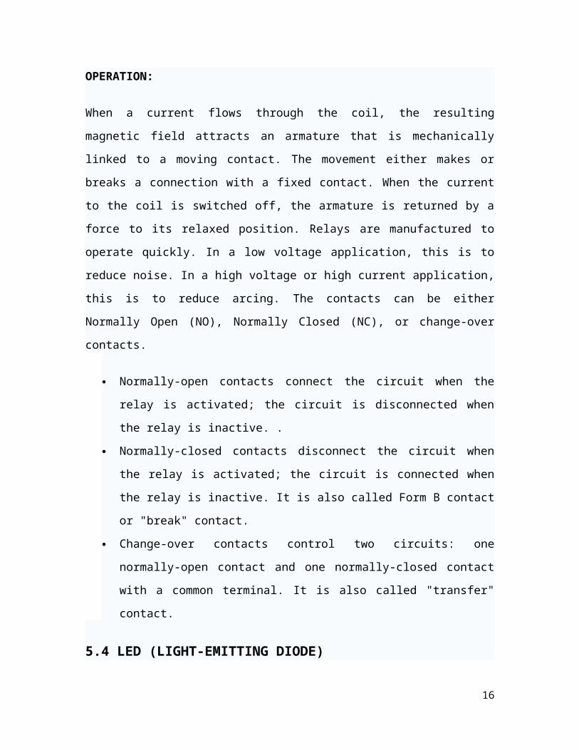
5.3RELAY
A relay is an electrical switch that opens and closes under control of another electrical
circuit. In the original form, the switch is operated by an electromagnet to open or close
one or many sets of contacts. It was invented by Joseph Henry in 1835.
11

FIG5.3(Relay)
OPERATION:
When a current flows through the coil, the resulting magnetic field attracts an armature
that is mechanically linked to a moving contact. The movement either makes or breaks a
connection with a fixed contact. When the current to the coil is switched off, the armature
is returned by a force to its relaxed position. Relays are manufactured to operate quickly.
In a low voltage application, this is to reduce noise. In a high voltage or high current
application, this is to reduce arcing. The contacts can be either Normally Open (NO),
Normally Closed (NC), or change-over contacts.
Normally-open contacts connect the circuit when the relay is activated; the circuit
is disconnected when the relay is inactive. .
Normally-closed contacts disconnect the circuit when the relay is activated; the
circuit is connected when the relay is inactive. It is also called Form B contact or
"break" contact.
Change-over contacts control two circuits: one normally-open contact and one
normally-closed contact with a common terminal. It is also called "transfer"
contact.
5.4 LED (LIGHT-EMITTING DIODE)
12
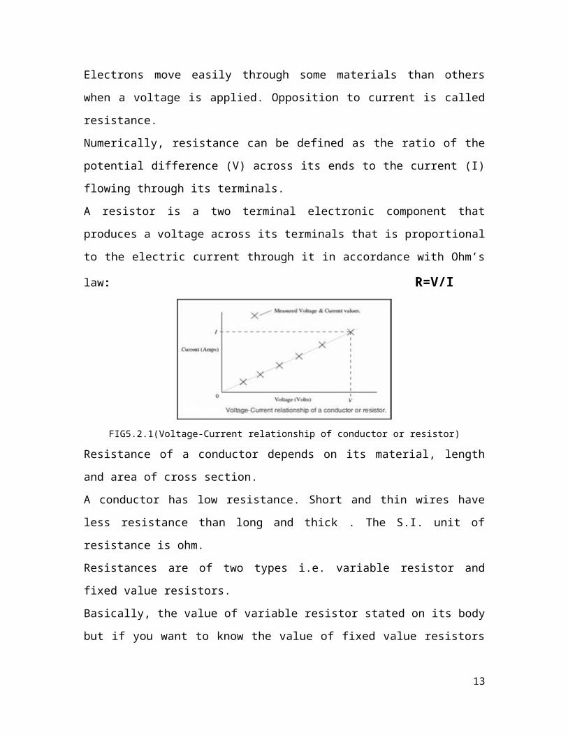
FIG5.4(Electronic Symbol)
A light-emitting diode (LED) is a semiconductor light source. LEDs are used as indicator
lamps in many devices, and are increasingly used for lighting.The LED is based on the
semiconductor diode. When a diode is forward biased (switched on), electrons are able to
recombine with holes within the device, releasing energy in the form of photons. This
effect is called electroluminescence and the color of the light (corresponding to the
energy of the photon) is determined by the energy gap of the semiconductor. An LED is
usually small in area (less than 1 mm2).
LEDs present many advantages over incandescent light sources including lower energy
consumption, longer lifetime, improved robustness, smaller size, faster switching, and
greater durability and reliance. However, they are relatively expensive and require more
precise current and heat management than traditional light sources. LEDs are available in
red, orange, amber, yellow, green, blue and white. Blue and white LEDs are much more
expensive than the other colors.The colour of an LED is determined by the
semiconductor material, not by the coloring of the 'package'.
LEDs are available in a wide variety of sizes and shapes. An LED must have a resistor
connected in series to limit the current through the LED, otherwise it will burn out almost
instantly.
Nonetheless these diodes are very useful as light emitters in visual display units and in
optically coupled circuits. They are used in arrays of different types for displaying
alphanumeric (letters and numbers) or supplying input power to lasers or for entering
information into optical computer memories and for numeral displays in hand-held or
pocket calculators.
CHARACTERISTICS
Following are the characteristics of LEDs:-
Low working voltages and currents.
Less power consumption.
Very fast action.
Small size and weight.
13
Emission of monochromatic light.
Extremely long life.
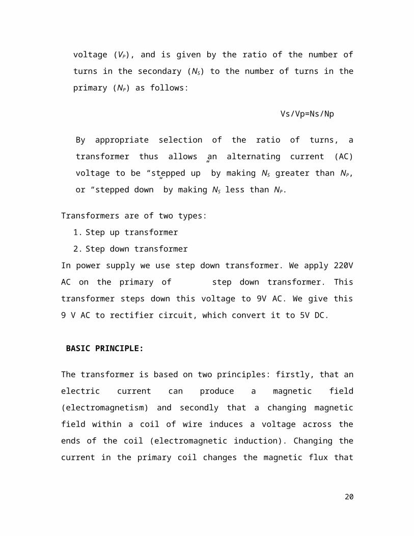
5.5 TRANSFORMER
A transformer is a device that transfers electrical energy from one circuit to
another through inductively coupled conductors- the transformer’s coils. A
varying current in the first or primary winding creates a varying magnetic field
through the secondary winding. This varying magnetic field induces a varying
EMF in the “secondary” winding. This effect is called mutual induction.
FIG5.5.1(Transformer)
In an ideal transformer, the induced voltage in the secondary winding (VS) is in
proportion to the primary voltage (VP), and is given by the ratio of the number of
turns in the secondary (NS) to the number of turns in the primary (NP) as follows:
Vs/Vp=Ns/Np
By appropriate selection of the ratio of turns, a transformer thus allows an alternating
current (AC) voltage to be “stepped up” by making NS greater than NP, or “stepped
down” by making NS less than NP.
14

Transformers are of two types:
1. Step up transformer
2. Step down transformer
In power supply we use step down transformer. We apply 220V AC on the primary of
step down transformer. This transformer steps down this voltage to 9V AC. We give this
9 V AC to rectifier circuit, which convert it to 5V DC.
BASIC PRINCIPLE:
The transformer is based on two principles: firstly, that an electric current can produce a
magnetic field (electromagnetism) and secondly that a changing magnetic field within a
coil of wire induces a voltage across the ends of the coil (electromagnetic induction).
Changing the current in the primary coil changes the magnetic flux that is developed. The
changing magnetic flux induces a voltage in the secondary coil.
5.6TRANSISTOR
A transistor is a three-terminal semiconductor device that can be used for amplification,
switching, voltage stabilization, signal modulation and many other functions. The
transistor is the fundamental building block of both digital and analog integrated circuits
- the circuitry that governs the operation of computers, cellular phones, and all other
modern electronics.
FIG5.6.1(Transistor)
15
A transistor is semi conductor device consisting of three regions separated by two P-N
junctions. The three regions are Base, Emitter & Collector. The base may be of N- type
or P- type. The emitter and collector have same impurities but different from that of base.
Thus if base is of N- type then emitter and collector are of P- type then transistor is called
P-N-P transistor and vice versa transistor is called N-P-N transistor.
The base is made thin and number density of majority carriers is always less than emitter
and collector. The base provides junction for proper interaction between emitter and
collector. Electrons are majority charge carriers in N- region and in P-region, holes are
the majority charge carriers. Thus two types of charge carriers are involved in current
flow through N-P-N or P-N-P transistor.
A transistor can be made by grouping the P and N type of semiconductors in one of the
following ways.
NPN
PNP
In the NPN transistor as the name suggest P type semiconductor is sandwiched between
two N type regions NPN & PNP transistor. In the PNP transistor N type semiconductor is
sandwiched between two p type regions.
The transistor's function is to amplify an electric current. Transistors are often used in
digital circuits as buffers to protect ICs. For example, when powering an electromagnetic
switch (called a 'relay').In analog circuits, transistors are used in amplifiers, (direct
current amplifiers, audio amplifiers, radio frequency amplifiers), and linear regulated
power supplies. Transistors are also used in digital circuits for eg microprocessors.
5.7 DIODE
A Diode is a semiconductor device, which allows the current to flow easily in one
direction, and provides a very high resistance when the current flows in the reverse
direction. The direction in which current flow easily, with little resistance, is called
forward direction and the opposing direction is called reverse direction.
16

FIG5.7.1(Diode)
A diode has two leads, anode and cathode. The conventional current can flow from
anode to the cathode but will face very high resistance when tries to flow from cathode to
the anode. so, allows the current to flow easily in one direction. The direction in which
current flow easily, with little resistance, is called forward direction and the opposing
direction is called reverse direction. The cathode is often marked by a band at one end.
FIG5.6.2(Characteristics)
Forward Biasing
When a battery is connected to this PN diode, the –ve terminal connected to the N type
will repel free electrons towards the junction, and the +ve terminal connected to the P
type will attract the free electrons from the junction, this will make the holes to move
towards the junction. This movement of electrons and the holes at the junction will make
the current to flow in the semiconductor diode as long as the battery is connected.
17

Current flow through the intrinsic,p-type &n-type semiconductors
Connected the battery to the diode, as explained above, is known as explained above, is
known as forward biasing the diode. Forward biasing means the voltage is applied in
such a way that the majority carrier (electron in N type and holes in P type are the major
current carriers.
Reverse Biasing
If the battery is connection in the reverse polarity, as shown in the figure 7C, i.e. the –ve
terminal to the P type and the +ve terminal to the N type, then the positive terminal will
attract electrons away from the junction and the negative terminal will attract the hole
away from the junction.
Depletion region in a diode.
This will stop the majority carriers from providing the current flow, only a small reverse
current due to minorities (holes in N type and electrons in P type) will flow. When
a voltage source is connected to diode this fashion it is known as reverse biasing.
18

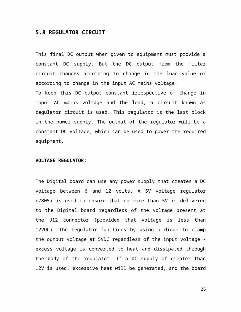
5.8 REGULATOR CIRCUIT
This final DC output when given to equipment must provide a constant DC supply. But
the DC output from the filter circuit changes according to change in the load value or
according to change in the input AC mains voltage.
To keep this DC output constant irrespective of change in input AC mains voltage and
the load, a circuit known as regulator circuit is used. This regulator is the last block in the
power supply. The output of the regulator will be a constant DC voltage, which can be
used to power the required equipment.
VOLTAGE REGULATOR:
The Digital board can use any power supply that creates a DC voltage between 6 and 12
volts. A 5V voltage regulator (7805) is used to ensure that no more than 5V is delivered
to the Digital board regardless of the voltage present at the J12 connector (provided that
voltage is less than 12VDC). The regulator functions by using a diode to clamp the output
voltage at 5VDC regardless of the input voltage - excess voltage is converted to heat and
dissipated through the body of the regulator. If a DC supply of greater than 12V is used,
excessive heat will be generated, and the board may be damaged. If a DC supply of less
than 5V is used, insufficient voltage will be present at the regulator output
.
FIG5.8.1(Voltage Regulator)
19
5.9GSM MODEM
A GSM modem is a specialized type of modem which accepts a SIM card, and operates
over a subscription to a mobile operator, just like a mobile phone. From the mobile
operator perspective, a GSM modem looks just like a mobile phone.
FIG5.9(GSM Modem)
When a GSM modem is connected to a computer, this allows the computer to use the
GSM modem to communicate over the mobile network. While these GSM modems are
most frequently used to provide mobile internet connectivity, many of them can also be
used for sending and receiving SMS and MMS messages.
20

CHAPTER 6: DATASHEETS OF IC’S
6.1.1PIN DIAGRAM OF IC AT89C51
FIG6.1.1(Pin Diagram)
6.1.2 FEATURES
• Compatible with MCS-51™ Products
• 4K Bytes of In-System Reprogrammable Flash Memory
Endurance: 1,000 Write/Erase Cycles
• Fully Static Operation: 0 Hz to 24 MHz
• Three-level Program Memory Lock
• 128 x 8-bit Internal RAM
• 32 Programmable I/O Lines
• Two 16-bit Timer/Counters
21

• Six Interrupt Sources
• Programmable Serial Channel
• Low-power Idle and Power-down Modes
6.1.3 DESCRIPTION
The AT89C51 is a low-power, high-performance CMOS 8-bit microcomputer with
4Kbytes of Flash programmable and erasable read only memory (PEROM). The
deviceis manufactured using Atmel’s high-density nonvolatile memory technology and is
compatible with the industry-standard MCS-51 instruction set and pinout. The on-chip
Flash allows the program memory to be reprogrammed in-system or by a conventional
nonvolatile memory programmer. By combining a versatile 8-bit CPU with Flash
on a monolithic chip, the Atmel AT89C51 is a powerful microcomputer which provides
a highly-flexible and cost-effective solution to many embedded control applications
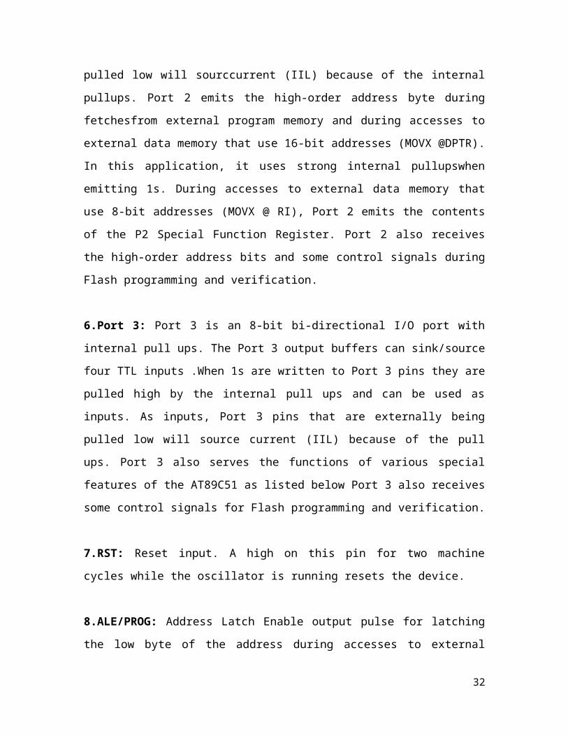
6.1.4PIN DESCRIPTION
1.VCC: Supply voltage.
2.GND: Ground.
3.Port 0:Port 0 is an 8-bit open-drain bi-directional I/O port. As anoutput port, each pin
can sink eight TTL inputs. When 1sare written to port 0 pins, the pins can be used as high
impedance inputs. Port 0 may also be configured to be the multiplexed loworder
address/data bus during accesses to external program and data memory. In this mode P0
has internal pullups. Port 0 also receives the code bytes during Flash programming , and
outputs the code bytes during program verification. External pullups are required during
program verification.
22

4.Port 1:Port 1 is an 8-bit bi-directional I/O port with internal pullups.The Port 1 output
buffers can sink/source four TTL inputs.When 1s are written to Port 1 pins they are
pulled high bythe internal pullups and can be used as inputs. As inputs, Port 1 pins that
are externally being pulled low will sourcecurrent (IIL) because of the internal pullups.
Port 1 also receives the low-order address bytes during Flash programming and
verification.
5.Port 2: Port 2 is an 8-bit bi-directional I/O port with internal pullups.The Port 2 output
buffers can sink/source four TTL inputs.When 1s are written to Port 2 pins they are
pulled high bythe internal pullups and can be used as inputs. As inputs,Port 2 pins that are
externally being pulled low will sourccurrent (IIL) because of the internal pullups. Port 2
emits the high-order address byte during fetchesfrom external program memory and
during accesses to external data memory that use 16-bit addresses (MOVX @DPTR). In
this application, it uses strong internal pullupswhen emitting 1s. During accesses to
external data memory that use 8-bit addresses (MOVX @ RI), Port 2 emits the contents
of the P2 Special Function Register. Port 2 also receives the high-order address bits and
some control signals during Flash programming and verification.
6.Port 3: Port 3 is an 8-bit bi-directional I/O port with internal pull ups. The Port 3
output buffers can sink/source four TTL inputs .When 1s are written to Port 3 pins they
are pulled high by the internal pull ups and can be used as inputs. As inputs, Port 3 pins
that are externally being pulled low will source current (IIL) because of the pull ups. Port
3 also serves the functions of various special features of the AT89C51 as listed below
Port 3 also receives some control signals for Flash programming and verification.
7.RST: Reset input. A high on this pin for two machine cycles while the oscillator is
running resets the device.
8.ALE/PROG: Address Latch Enable output pulse for latching the low byte of the
address during accesses to external memory. This pin is also the program pulse input
(PROG) during Flash programming. In normal operation ALE is emitted at a constant
23

rate of 1/6 the oscillator frequency, and may be used for external timing or clocking
purposes. Note, however, that one ALE
9.PORT PIN ALTERNATE FUNCTIONS
P3.0 RXD (serial input port)
P3.1 TXD (serial output port)
P3.2 INT0 (external interrupt 0)
P3.3 INT1 (external interrupt 1)
P3.4 T0 (timer 0 external input)
P3.5 T1 (timer 1 external input)
P3.6 WR (external data memory write strobe)
P3.7 RD (external data memory read strobe)
pulse is skipped during each access to external Data Memory .If desired, ALE operation
can be disabled by setting bit 0 of SFR location 8EH. With the bit set, ALE is active only
during a MOVX or MOVC instruction. Otherwise, the pin is weakly pulled high. Setting
the ALE-disable bit has no effect if the microcontroller is in external execution mode.
10.PSEN: Program Store Enable is the read strobe to external program memory. When
the AT89C51 is executing code from external program memory, PSEN is activated twice
each machine]cycle, except that two PSEN activations are skipped during each access to
external data memory.
11.EA/VPP: External Access Enable. EA must be strapped to GND in order to enable the
device to fetch code from external program memory locations starting at 0000H up to
FFFFH .Note, however, that if lock bit 1 is programmed, EA will be internally latched on
reset .EA should be strapped to VCC for internal program executions .This pin also
receives the 12-volt programming enable voltage (VPP) during Flash programming, for
parts that require12-volt VPP.
12.XTAL1:Input to the inverting oscillator amplifier and input to the internal clock
operating circuit.
24

13.XTAL2: Output from the inverting oscillator amplifier.
OSCILLATOR CHARACTERISTICS:
XTAL1 and XTAL2 are the input and output, respectively, of an inverting amplifier
which can be configured for use as an on-chip oscillator, as shown in Figure 1. Either a
quartz crystal or ceramic resonator may be used. To drive the device from an external
clock source, XTAL2 should be left unconnected while XTAL1 is driven as shown in
Figure 2.There are no requirements on the duty cycle of the external clock signal, since
the input to the internal clocking circuitry is through a divide-by-two flip-flop, but
minimum and maximum voltage high and low time specifications must be observed.
6.2.1 PIN DIAGRAM OF IC MAX-232
FIG6.2.1(Pin Diagram)
It runs on a single chip supply (+5 volts), and requires a few external capacitors. There is
another version, the MAX233 which requires no external parts. It is, however, a little
larger physically, and also costs about 75% more than the MAX232A.
25
Here is a diagram of the internals of the MAX232A. It shows a double charge pump
voltage doubler and a +10v to -10v voltage inverter. The voltages output are used to
generate the RS-232 compliant signals. The MAX232A has provisions for two serial
ports on the same physical package. Most people only connect one of them.
6.2.2 78XX(VOLTAGE REGULATOR)
FIG6.2.2(7805)
The 78xx (also sometimes known as LM78xx) series of devices is a family of self-
contained fixed linear voltage regulator integrated circuits. The 78xx family is a very
popular choice for many electronic circuits which require a regulated power supply, due
to their ease of use and relative cheapness. When specifying individual ICs within this
family, the xx is replaced with a two-digit number, which indicates the output voltage the
particular device is designed to provide (for example, the 7805 has a 5 volt output, while
the 7812 produces 12 volts). The 78xx line are positive voltage regulators, meaning that
they are designed to produce a voltage that is positive relative to a common ground.
There is a related line of 79xx devices which are complementary negative voltage
regulators. 78xx and 79xx ICs can be used in combination to provide both positive and
negative supply voltages in the same circuit, if necessary.
78xx ICs have three terminals and are most commonly found in the TO220 form factor,
although smaller surface-mount and larger TO3 packages are also available from some
manufacturers. These devices typically support an input voltage which can be anywhere
26

from a couple of volts over the intended output voltage, up to a maximum of 35 or 40
volts, and can typically provide up to around 1 or 1.5 amps of current (though smaller or
larger packages may have a lower or higher current rating).
ADVANTAGES:
The 7805 series has several key advantages over many other voltage regulator circuits
which have resulted in its popularity:
7805 series ICs do not require any additional components to provide a constant,
regulated source of power, making them easy to use, as well as economical, and
also efficient uses of circuit board real estate.
78xx series ICs have built-in protection against a circuit drawing too much power. They
also have protection against overheating and short-circuits, making them quite robust in
most applications. In some cases, the current-limiting features of the 78xx devices can
provide protection not only for the 78xx itself, but also for other parts of the circuit.
27

CHAPTER 7: PCB FABRICATION
7.1 INTRODUCTION
A PCB is used to mechanically support and electrically connect electronic components
using conductive pathways, tracks or etched from copper sheets. It is also referred to as
printed wiring board (PWB). A PCB populated with electronic components is a printed
circuit assembly (PCA), also known as a printed circuit board assembly (PCBA).PCBs is
inexpensive, and can be highly reliable. They require much more layout effort and higher
initial cost than either wire-wrapped or point-to-point constructed circuits, but are much
cheaper and faster for high-volume production. One of the most discouraging things
about making a hardware project is building PCB. Due to the improvements in printing
technologies it is now relatively easy to make inexpensive high quality PCB's at home.
PCB stands for Printed Circuit Board. It is of two types:
a) General purpose: It is already drilled and etched.
b) Special purpose: It requires step by step process of making layout then etching and
then drilling.
7.2PCB CONSTRUCTION
The different processes that take place in the fabrication of a PCB are as follows:
a) Layout designing
b) Transfer of pattern on copper board.
c) Drying
d) Etching
e) Tinning
f) Drilling
g) Soldering
28

h) Surface cleaning
i) Final inspection of PCB
a) LAYOUT DESIGNING
First of all layout design of the circuit switch is to be traced on the PCB, is prepared. The
layout of a PCB has to incorporate all the information on the board one can go to the art
work preparation. The detailed circuit diagram is very important for the layout designer
but he must also familiar with the design concept & with the philosophy behind the
equipment. In this process the layout designer, traces the circuit on a graph paper. By this
process he marks where the holes should be. Thus the circuit, which is to be traced on the
PB, is firstly traced on the graph paper or its layout is designed. In layout designing the
distance between the copper tracks & length, size etc. of components are also taken into
consideration.
FIG7.2.1(Layout Designing)
b) TRANSFER OF PATTERN
After designing the art work on the graph paper, we transferred it onto the trace paper. The
conductor pattern is then transferred n to the copper clad lamination with the help of
carbon paper. By this the pattern gets transferred on the copper clad lamination.
29

c) ETCHING
Etching is done to remove all the unwanted copper which is present on the portion other
than the pattern on the PCB. For this the PCB is kept dipped in the solution (Fe.Cl2) & two
or three drops of HCL. The chemicals react with copper & dissolve it. After some hours of
time we get the PCB left with only copper tracks on it.
d) TINNING
The board is tinned using a soldering iron and a small piece of tinned solderwick. Tinning
isn't absolutely necessary but it improves the appearance of the board, and prevents the
copper from oxidizing before it's time to solder the parts to the board.
e)DRILLING
Drilling of component mounting holes into PCB is the most important mechanical
matching operation in PCB production process. Holes are made by drilling where ever a
superior hole finish in is required. Therefore, drilling is applied by all the professional
grade PCB manufacturers & generally in all smaller PCB production plants &
laboratories.
f)SOLDERING
Soldering is the process of joining two metallic conductors, the joint where the two
metallic conductors are to be joined or fused is heated with a device called soldering iron
and then an alloy of tin and lead called solder is applied which melts and cover the joint.
The solder cools and solidifies quickly to ensure a good and durable connection between
the joined metals. Covering the joint with solder prevents oxidation.
30

EQUIPMENTS REQUIRED:
The various tools and equipments required for construction of a PCB are given below: -
1. Solder kit consist of:
a. Soldering iron.
b. Soldering wire.
c. Flux
2.Tweezer
3.Cutter
4.Multi-meter (Measuring instrument).
PRECAUTIONS FOR PRACTICAL:
1. The quantity of soldering of component on PCB should be good quantity.
2. The component fitted on the PCB should loosely fit.
3. Use ferric chloride safely.
4. Add ferric chloride to the water, not water to the ferric chloride.
g)SURFACE CLEANING
After drilling the surface is cleaned so that the scraps may be removed which are settled on
the board during drilling.
h) FINAL INSPECTION OF PCB
After complete fabrication, PCB is inspected for any defect such as short circuit or
open circuit. If no defect found, then the PCB will be directly considered for operation.
31
CHAPTER 8: SCOPE AND APPLICATIONS
I. Introduction of Farming with Advance Technology.
II. Applicable for Water level measurement in borewell,waterfields,
tubewells etc.
III. Vast scope due to day-by-day advancement in Farming Techniques.
IV. Efficient, Simple, Portable, Affordable systems like these are required.
V. Increase in the need of Production requires proper supply of water in fields
this system can provide help to the farmers.
32

CHAPTER 9: LIST OF COMPONENTS
COMPONENTS NO. COST(Rs)
IC1-AT89C51 microcontroller 1 40
IC2 - MAX232 driver 1 10
IC3 - 7805, 5V regulator 1 5
BR1 - 1A bridge rectifier 1 10
T1, T2 - BC548 NPN
transistor
2 5
LED1, LED2 - 5mm light-
emitting diodes
2 2
D1 - 1N4007 rectifier diode 1 5
R1 - 1-kilo –ohm 1 1
R3, R4 - 10-kilo-ohm 2 2
R5 - 100-kilo-ohm 1 2
C1 - 1000μF, 25V electrolytic 1 5
C2, C4-C7 - 0.1μF ceramic 3 5
C3 - 10μF, 16V electrolytic 1 10
C8, C9 - 22pF ceramic 2 5
X1 - 220V AC primary to 12V
250mA secondary transformer
1 30
RL1 - 12V, 1C/O relay 1 15
S1 - Tactile switch 1 2
XTAL - 11.0592MHz crystal 1 5
GSM modem - SIM300 V7.03
modem
1 1300
Sensors - Two water-level
steel sensor Rods
2 2
TABLE9.1(List of Components)
33

CHAPTER 10: TROUBLE SHOOTING
1. PCB Designing should be done carefully.
2. Selection of components should be done carefully.
3. Due to the dry soldering some connection may remain loose.
4. Short circuiting should be avoided during connections.
5.Components should be mounted carefully.
34

CHAPTER 11: REFERENCES
http://ezine.efymag.com
EFY MAGZINE (Edition- May 2012)
35