Project Olympus AMD EPYC Motherboard Specification
54
Project Olympus AMD EPYC™ Processor Motherboard Specification Author: Fenghua Shen, Senior Hardware Engineer, Microsoft Mark A. Shaw, Principal Hardware Engineering Manager, Microsoft
Transcript of Project Olympus AMD EPYC Motherboard Specification

Project Olympus AMD EPYC™ Processor
Motherboard Specification
Author:
Fenghua Shen, Senior Hardware Engineer, Microsoft
Mark A. Shaw, Principal Hardware Engineering Manager, Microsoft

Open Compute Project • Project Olympus AMD EPYC™ Processor Motherboard Specification
http://opencompute.org ii
Revision History
Date Description
11/1/17 Version 1.0

Open Compute Project • Project Olympus AMD EPYC™ Processor Motherboard Specification
http://opencompute.org iii
© 2017 Microsoft Corporation.
As of November 1, 2017, the following persons or entities have made this Specification available under the Open Web
Foundation Final Specification Agreement (OWFa 1.0), which is available at http://www.openwebfoundation.org/legal/the-
owf-1-0-agreements/owfa-1-0
Microsoft Corporation.
You can review the signed copies of the Open Web Foundation Agreement Version 1.0 for this Specification at Project Olympus
License Agreements, which may also include additional parties to those listed above.
Your use of this Specification may be subject to other third party rights. THIS SPECIFICATION IS PROVIDED "AS IS." The
contributors expressly disclaim any warranties (express, implied, or otherwise), including implied warranties of merchantability,
non-infringement, fitness for a particular purpose, or title, related to the Specification. The entire risk as to implementing or
otherwise using the Specification is assumed by the Specification implementer and user. IN NO EVENT WILL ANY PARTY BE
LIABLE TO ANY OTHER PARTY FOR LOST PROFITS OR ANY FORM OF INDIRECT, SPECIAL, INCIDENTAL, OR CONSEQUENTIAL
DAMAGES OF ANY CHARACTER FROM ANY CAUSES OF ACTION OF ANY KIND WITH RESPECT TO THIS SPECIFICATION OR ITS
GOVERNING AGREEMENT, WHETHER BASED ON BREACH OF CONTRACT, TORT (INCLUDING NEGLIGENCE), OR OTHERWISE,
AND WHETHER OR NOT THE OTHER PARTY HAS BEEN ADVISED OF THE POSSIBILITY OF SUCH DAMAGE.
CONTRIBUTORS AND LICENSORS OF THIS SPECIFICATION MAY HAVE MENTIONED CERTAIN TECHNOLOGIES THAT ARE MERELY
REFERENCED WITHIN THIS SPECIFICATION AND NOT LICENSED UNDER THE OWF CLA OR OWFa. THE FOLLOWING IS A LIST OF
MERELY REFERENCED TECHNOLOGY: INTELLIGENT PLATFORM MANAGEMENT INTERFACE (IPMI); I2C IS A TRADEMARK AND
TECHNOLOGY OF NXP SEMICONDUCTORS ; EPYC IS A TRADEMARK AND TECHNOLOGY OF ADVANCED MICRO DEVICES INC.;
ASPEED AST 2400/2500 FAMILY PROCESSORS IS A TECHNOLOGY OF ASPEED TECHNOLOGY INC.; MOLEX NANOPITCH, NANO
PICOBLADE, AND MINI-FIT JR AND ASSOCIATED CONNECTORS ARE TRADEMARKS AND TECHNOLOGIES OF MOLEX LLC;
WINBOND IS A TRADEMARK OF WINBOND ELECTRONICS CORPORATION; NVLINK IS A TECHNOLOGY OF NVIDIA; INTEL XEON
SCALABLE PROCESSORS, INTEL QUICKASSIST TECHNOLOGY, INTEL HYPER-THREADING TECHNOLOGY, ENHANCED INTEL
SPEEDSTEP TECHNOLOGY, INTEL VIRTUALIZATION TECHNOLOGY, INTEL SERVER PLATFORM SERVICES, INTEL MANAGABILITY
ENGINE, AND INTEL TRUSTED EXECUTION TECHNOLOGY ARE TRADEMARKS AND TECHNOLOGIES OF INTEL CORPORATION;
SITARA ARM CORTEX-A9 PROCESSOR IS A TRADEMARK AND TECHNOLOGY OF TEXAS INSTRUMENTS; GUIDE PINS FROM
PENCOM; BATTERIES FROM PANASONIC. IMPLEMENTATION OF THESE TECHNOLOGIES MAY BE SUBJECT TO THEIR OWN LEGAL
TERMS.
iv November 1, 2017
Contents 1 Project Olympus Specifications List ............................................................................................................... 1
2 Overview ....................................................................................................................................................... 1
3 Background ................................................................................................................................................... 2
4 Block Diagram ............................................................................................................................................... 2
5 Features ........................................................................................................................................................ 3
5.1 CPUs ............................................................................................................................................................. 4
5.2 DIMMs .......................................................................................................................................................... 4
5.3 PCIe Support ................................................................................................................................................. 5
5.3.1 CPU PCIe Mapping ................................................................................................................................... 5
5.3.2 PCIe x8 Slots ............................................................................................................................................. 5
5.3.3 PCIe x16/32 Slots ..................................................................................................................................... 5
5.3.4 PCIe Cables ............................................................................................................................................... 6
5.3.5 M.2 Modules ............................................................................................................................................ 6
5.4 PCIe/SATA Expansion ................................................................................................................................... 6
5.5 SATA Storage ................................................................................................................................................ 6
5.6 TPM Module ................................................................................................................................................. 6
6 Management Subsystem ............................................................................................................................... 7
6.1 BMC .............................................................................................................................................................. 8
6.2 BMC DRAM ................................................................................................................................................... 8
6.3 BMC Boot Flash ............................................................................................................................................ 8
6.4 BIOS Flash ..................................................................................................................................................... 8
6.5 1GbE PHY ...................................................................................................................................................... 8
6.6 UARTs ........................................................................................................................................................... 9
6.7 VGA .............................................................................................................................................................. 9
6.8 I2C ................................................................................................................................................................ 9
6.8.1 FRUID PROM .......................................................................................................................................... 11
6.8.2 Temperature Sensors ............................................................................................................................. 11
6.8.3 PCIe Devices ........................................................................................................................................... 12
6.8.4 Voltage Regulators ................................................................................................................................. 12
6.8.5 Hot Swap Controllers ............................................................................................................................. 12
6.8.6 Clock Buffers .......................................................................................................................................... 12
6.9 JTAG ........................................................................................................................................................... 12
6.10 Jumpers ...................................................................................................................................................... 13

Open Compute Project • Project Olympus AMD EPYC™ Processor Motherboard Specification
http://opencompute.org v
6.11 LEDs ............................................................................................................................................................ 13
6.11.1 UID LED .............................................................................................................................................. 14
6.11.2 Power Status LED ............................................................................................................................... 14
6.11.3 Attention LED .................................................................................................................................... 15
6.11.4 PSU Status LEDs ................................................................................................................................. 15
6.12 Fan Control ................................................................................................................................................. 15
7 Power Management .................................................................................................................................... 15
7.1 Rack Management ..................................................................................................................................... 16
7.2 PSU Management ...................................................................................................................................... 17
7.3 Hot Swap Controller ................................................................................................................................... 18
7.4 Power Capping ........................................................................................................................................... 18
7.5 PWRBRK# ................................................................................................................................................... 19
7.6 MEM VRHOT and EVENT_L ........................................................................................................................ 19
8 Motherboard Layout ................................................................................................................................... 20
9 Serviceability ............................................................................................................................................... 22
9.1 Debug features ........................................................................................................................................... 22
9.2 LED Visibility ............................................................................................................................................... 22
10 Motherboard Interfaces .............................................................................................................................. 22
10.1 PCIe x8 Connectors ..................................................................................................................................... 23
10.2 PCIe x16 Connectors ................................................................................................................................... 25
10.3 PCIe x32 Connector .................................................................................................................................... 27
10.4 PCIe MiniSAS HD Connectors ...................................................................................................................... 31
10.5 M.2 Connectors .......................................................................................................................................... 32
10.6 SATA Cable Ports ........................................................................................................................................ 33
10.7 SATA Power Connector ............................................................................................................................... 33
10.8 SATA Power Expansion Connector.............................................................................................................. 34
10.9 12V Power Connector ................................................................................................................................. 35
10.10 Management Connector ........................................................................................................................ 36
10.11 Management Expansion Connector ....................................................................................................... 37
10.12 OCuLink x8 Connector ............................................................................................................................ 37
10.13 NCSI Connector ...................................................................................................................................... 39
10.14 USB 2.0 Internal Header ......................................................................................................................... 40
10.15 Fan Control Connector ........................................................................................................................... 41
10.16 TPM Connector ...................................................................................................................................... 42

vi November 1, 2017
10.17 Connector Quality .................................................................................................................................. 43
11 Electrical Specifications ............................................................................................................................... 43
11.1 Input Voltage, Power, and Current ............................................................................................................. 43
11.2 Current Interrupt Protection and Power, Voltage, and Current Monitoring .............................................. 43
11.3 Filtering and Capacitance ........................................................................................................................... 44
11.4 Grounding and Return ................................................................................................................................ 44
12 Physical Specifications ................................................................................................................................. 44
13 Environmental ............................................................................................................................................. 45
14 Electromagnetic Interference Mitigation ..................................................................................................... 46

Open Compute Project • Project Olympus AMD EPYC™ Processor Motherboard Specification
http://opencompute.org vii
Table of Figures Figure 1. Top Level Block Diagram ................................................................................................................ 2
Figure 2. Management Block Diagram .......................................................................................................... 7
Figure 3. UART Block Diagram ...................................................................................................................... 9
Figure 4. I2C Block Diagram ........................................................................................................................ 10
Figure 5. DDR4 SPD I2C Block Diagram ....................................................................................................... 11
Figure 6. JTAG Block Diagram ..................................................................................................................... 13
Figure 7. Rack Interface Block Diagram ...................................................................................................... 16
Figure 8. PROCHOT Block Diagram ............................................................................................................ 19
Figure 9. PWRBRK# Block Diagram ............................................................................................................. 19
Figure 10. MEM VRHOT Block Diagram ...................................................................................................... 20
Figure 11. MEM EVENT_L Block Diagram ................................................................................................... 20
Figure 12. Motherboard Layout .................................................................................................................. 21
Figure 13. SATA Power Connector Pin Numbering ..................................................................................... 34
Figure 14. SATA Power Expansion Connector Pin Numbering .................................................................... 34
Figure 15. Mini-Fit Connector Pin Numbering ............................................................................................ 36
Figure 16. Server Management Connector Pin Numbering ........................................................................ 36
Figure 17. OCuLink x8 Pin Numbering ........................................................................................................ 39
Figure 18. NCSI Connector Pin Numbering ................................................................................................. 40
Figure 19. Internal USB Connector Pinout .................................................................................................. 40
Figure 20. Fan Control Connector Pin Numbering ...................................................................................... 42
Figure 21. TPM Connector .......................................................................................................................... 42
Figure 22. Example Motherboard Drawing ................................................................................................. 45

viii November 1, 2017
Table of Tables Table 1. List of Specifications ....................................................................................................................... 1
Table 2. CPU PCIe Port Mapping ................................................................................................................... 5
Table 3. Jumpers ......................................................................................................................................... 13
Table 4. LEDs ............................................................................................................................................... 14
Table 5. Server Power Status LED Description ............................................................................................ 14
Table 6. Attention LED Description ............................................................................................................. 15
Table 7. Slot ID Decode ............................................................................................................................... 16
Table 8. PCIe x8 connector pinout .............................................................................................................. 23
Table 9. PCIe x16 connector pinout ............................................................................................................ 25
Table 10. PCIe x32 Connector Pinout - 200 Pin........................................................................................... 27
Table 11. PCIe x32 Connector Pinout - 60 Pin............................................................................................. 30
Table 12. PCIe Cable Connector Pinout ...................................................................................................... 31
Table 13. M.2 connector pinout ................................................................................................................. 32
Table 14. SATA Power Connector ............................................................................................................... 33
Table 15. SATA Power Expansion Connector Pinout .................................................................................. 34
Table 16. 12V Power Connector ................................................................................................................. 35
Table 17. 1U Management Connector ........................................................................................................ 36
Table 18. Management Expansion Connector ............................................................................................ 37
Table 19. OCuLink x8 Connector ................................................................................................................. 38
Table 20. NCSI Connector ........................................................................................................................... 39
Table 21. Internal USB Connector ............................................................................................................... 40
Table 22. Fan Control Connector ................................................................................................................ 41
Table 23. TPM Connector Pinout ................................................................................................................ 42
Table 24. Input Power Requirements ......................................................................................................... 43
Table 25. Environmental Requirement ....................................................................................................... 45

Open Compute Project • Project Olympus AMD EPYC™ Processor Motherboard Specification
http://opencompute.org 1
1 Project Olympus Specifications List Table 1 lists the Project Olympus system specifications.
Table 1. List of Specifications
Specification title Description
Project Olympus Server Rack Specification
Describes the mechanical rack hardware used in the system
Project Olympus Server Mechanical Specification
Describes the mechanical structure for the server used in the system.
Project Olympus Universal Motherboard Specification
Describes the server motherboard general requirements.
Project Olympus PSU Specification Describes the Power Supply Unit (PSU) used in the server
Project Olympus Power Management Distribution Unit Specification
Describes the Power Management Distribution Unit (PMDU).
Project Olympus Rack Manager Specification
Describes the Rack Manager PCBA used in the PMDU.
This document is intended for designers and engineers who will be building servers for Project Olympus
systems.
2 Overview This specification describes the Project Olympus AMD Server Motherboard. This is an implementation
specific specification under the Project Olympus Universal Motherboard Specification.
Refer to respective specifications for other elements of the Project Olympus system such as Power
Supply Unit (PSU), Rack Manager (RM), Power and Management Distribution Unit (PMDU), and Server
Rack.
This specification covers block diagram, management sub-system, power management, FPGA Card
support, IO connectors, and physical specifications of the Server Motherboard.

2 November 1, 2017
3 Background The server motherboard is the computational element of the server. The motherboard includes a full
server management solution and supports interfaces to integrated or rear-access 12V Power Supply
Units (PSUs).
The Server optionally interfaces to a rack-level Power and Management Distribution Unit (PMDU).
The PMDU provides power to the Server and interfaces to the Rack Manager (RM).
The motherboard design provides optimum front-cable access (cold aisle) for external IO such as
networking and storage as well as standard PCIe cards. This enables flexibility to support many
configurations.
4 Block Diagram Figure 1 shows the baseline block diagram describing general requirements for the server motherboard.
Figure 1. Top Level Block Diagram
CPU0
CPU1
L2L1
M2
M1
PCIe x16 SLOT #5
PCIe x8 SLOT #1
PCIe x8 SLOT #2
GMI3
CH
A
CH
B
CH
C
CH
D
CH
E
CH
F
DIM
M
DIM
M
DIM
M
DIM
M
DIM
M
DIM
M
DIM
M
DIM
M
DIM
M
DIM
M
DIM
M
DIM
M
O2O1N2N1M2M1I1I2J1J2
Oculink x8
BMC
DDR4512MB
FLASH #132MBSPI
UART
DDR4
LPC
SMBUS
M.2 Module #2
M.2 Module #1
DebugConnector
USB2B
NCSI
FLASH #232MB
PCIe
VGA VGA
NCSIConnector
RGMII RJ451GbE PHY
CH
G
CH
H
Front Panel SFP+
NIC
Front Panel SFP+
x4 MINISAS HD#1
x4 MINISAS HD#2
DIM
M
DIM
M
DIM
M
DIM
M
K1K2L1L2
GMI0
GMI1
GMI2
GMI1
GMI2
GMI3
GMI4
M.2 Module #4
M.2 Module #3
CH
A
CH
B
CH
C
CH
D
CH
E
CH
F
DIM
M
DIM
M
DIM
M
DIM
M
DIM
M
DIM
M
DIM
M
DIM
M
DIM
M
DIM
M
DIM
M
DIM
M
G2G1F2F1E2E1A1A2B1B2
CH
G
CH
H
DIM
M
DIM
M
DIM
M
DIM
M
C1C2D1D2
P0[7:0]
P1[7:4]
P1[11:8]
P2[15:0]
P3[7:0]
P3[11:8]
P3[15:12]
P0[15:8]
P1[12]
SATA3 x1P1[3]
P1[2]
P1[1]
P1[0]
SATA2 x1
SATA1 x1
SATA0 x1
P1[15:13]
P3
[3:0
]
P3
[7:4
]
P2[15:0]
P0[15:0]
P3[15:8]
P1
[15
:0]
H2H1P2P1
PCIe x16 SLOT #3
PCIe x32 SLOT #4
6Gb/s
6Gb/s
6Gb/s
6Gb/s
Gen3 x4 (8GB/s)
Gen3 x4 (8GB/s)
Gen3 x4 (8GB/s)
Gen3 x4 (8GB/s)
Gen3 x8 (16GB/s)
Gen3 x8 (16GB/s)
Gen3 x16 (32GB/s)
Gen3 x16 (32GB/s)
Gen3 x16 (32GB/s)
Gen3 x16 (32GB/s)USB0(0)
Front PanelUSB 3.0
Front PanelUSB 3.0USB0(1)
5Gb/s
5Gb/s
InternalUSB 2.0 TypeA
USB1(2)480Mb/s
Gen3 x8 (16GB/s)
Gen3 x1 (2GB/s)
BIOS FLASH32MB
TPM 2.0
SPI33MHz
BIOS FLASH32MB LPC
USB0(1)
10Gb/s
10Gb/s
Gen3 x8 (16GB/s)
SMBUS
USB2A
USB1(2)
480Mb/s
480Mb/s
33MHz

Open Compute Project • Project Olympus AMD EPYC™ Processor Motherboard Specification
http://opencompute.org 3
5 Features
The motherboard includes support for the following features:
Processor
Platform AMD EPYC™ platform
CPU AMD EPYC™ processors
Sockets Dual socket operation
TDP Wattage Up to 180W (Support for all server class SKUs)
Memory
DIMM Slots 32 total DIMM slots
16 DIMMs per CPU
2 DIMMs per channel
DIMM Type Double data rate fourth generation (DDR4) Registered DIMM (RDIMM) with
Error-Correcting Code (ECC)
DIMM Speed DDR4-2400 (2DPC), DDR4-2666 (1DPC)
DIMM Size 16GB, 32GB, 64GB
Capacities
Supported
128GB, 256GB, 512GB, 756GB, 1TB, 2TB (TBD)
Storage
SATA 4 local ports @ 6.0 Gb/s (SATA x1)
4 expansion ports @ 6.0Gb/s (MiniSAS HD)
Server Management
Chipset BMC Aspeed AST2520/AST2500
Interface Representational State Transfer (REST) API
Windows Management Instrumentation (WMI)
Open Management Interface (OMI)
Command-Line Interface (CLI)
System Firmware

4 November 1, 2017
BIOS Unified Extensible Firmware Interface (UEFI), AMI
BMC AMI
Security Trusted Platform Module (TPM 2.0) Secure Boot
PCI-Express Expansion
2 PCIe x8 Slots Supports PCIe M.2 Riser Cards
2 PCIe x16 Slots Supports standard PCIe x16 cards
1 PCIe x32 Slot Supports standard PCIe x16 or custom PCIe x32 cards
4 M.2 Slots Supports 60mm, 80mm, and 110mm M.2 Cards
1 PCIe x8 Expansion 1 OCuLink x8
2 PCIe x4 Expansion 2 MiniSAS HD PCIe x4
Networking
LOM 2x 10GbE from CPU0 through NIC on SFP+ Connector
MGMT 1x 1GbE from BMC to RJ45 Connector
5.1 CPUs
The server supports two AMD EPYC™ CPUs for all server class SKUs. The maximum TDP to be supported
is 180W.
5.2 DIMMs
The motherboard supports 32 DDR4 RDIMMs with 16 RDIMMs per CPU socket. It supports all available
configurations for single, dual, and quad rank RDIMMs per AMD guidelines. The DIMM sockets are also
able to support NVDIMM as described in this document. The DIMM pitch is 296.85mils.
The motherboard is designed to support the following technologies but use of these technologies is not
validated.
• LRDIMM
• 3DS RDIMM
• DDR4 NVDIMM with 12V power through the DIMM connector

Open Compute Project • Project Olympus AMD EPYC™ Processor Motherboard Specification
http://opencompute.org 5
5.3 PCIe Support
5.3.1 CPU PCIe Mapping
Table 5 describes the PCIe port mapping between the CPUs and the PCIe endpoints.
Table 2. CPU PCIe Port Mapping
CPU PCIe Bus Destination
0 P0(15:8) PCIe Slot #2
0 P0(7:0) PCIe Slot #1
0 P1(15:13) Reserved
0 P1(12) BMC
0 P1(11:8) MiniSAS HD #2
0 P1(7:4) MiniSAS HD #1 or SATA[7:4]
0 P1(3:0) SATA[3:0]
0 P2(15:0) PCIe Slot #3
0 P3(15:12) M.2 Module #1
0 P3(11:8) M.2 Module #2
0 P3(7:0) NIC
1 P0(15:0) PCIe Slot #4
1 P1(15:0) PCIe Slot #5
1 P2(15:0) PCIe Slot #4
1 P3(15:8) OCuLink x8
1 P3(7:4) M.2 Module #4
1 P3(3:0) M.2 Module #3
5.3.2 PCIe x8 Slots
The motherboard supports two PCIe x8 slots to slots 1 and 2 as shown in Figure 2. Each slot supports 1x8
and 2x4 bifurcation. 2x4 bifurcation is supported at the connector with the addition of a 2nd PCIe clock to
the standard PCIe pinout. The primary purpose of the slots is to support M.2 Modules with each slot
capable of supporting two modules. Use of the modules requires a PCIe riser edge card to connect the
modules to the PCIe bus. The riser is capable of supporting 60mm, 80mm, and 110mm M.2 Modules.
5.3.3 PCIe x16/32 Slots
The motherboard supports two PCIe x16 slots and one PCIe x32 (2x16) slot as shown in Figure 2. Each
slot supports a standard PCIe form factor card using a riser card to interface to the PCIe connector. The
size of the card supported is dependent on the height of the tray assembly. 1U trays can support FHHL
PCIe cards. 2U trays can support FHFL cards. Note that Slot #4 is targeted for use by FPGA cards
requiring two PCIe x8 channels and this is the default configuration. In this case, additional PCIe can be
cabled from the OCuLink x8 connector.

6 November 1, 2017
All slots support bifurcation below 1x16 but utilize the standard PCIe connector pinout and do not
contain additional clocks. Additional clocks required for bifurcation below 1x16 must be handled with
buffer circuitry on the PCIe card.
5.3.4 PCIe Cables
The motherboard supports a single OCuLink x8 connector for the primary purpose of expanding PCIe
support to Slot#4 to 24 lanes. PCIe clock and control signals are not supported by the implementation.
Physical cabling must avoid any FHHL PCIe card located in Slot #5.
5.3.5 M.2 Modules
The motherboard supports M.2 modules through any of the following methods:
• Standard M.2 connector mounted directly on the motherboard. The motherboard supports up to four on-board M.2 modules.
• M2 Riser Cards in Slots #1 and #2: PCIe Riser card supporting up to two M.2. modules in each slot. All four modules are connected to a PCIe endpoint on CPU0.
• Quad M.2 Carrier Card (OCP AVA): FHHL PCIe Card in standard PCIe format supporting up to four
M.2 modules.
For both motherboard and PCIe Card applications, the supported M.2 modules are 60mm, 80mm, and
110mm dual sided form factors (Type 2260, 2280, and 22110).
5.4 PCIe/SATA Expansion
The motherboard supports two MiniSAS-HD x4 connectors, one for PCIe expansion, one for optional
PCIe or SATA expansion from the high-speed IO ports on the CPU0. PCIe expansion only miniSAS-HD
connector is connected to CPU0 PCIe P1[11:8] and PCIe/SATA expansion miniSAS-HD connector is
connected to CPU0 PCIe P1[7:4]. The functionality of the ports (PCIe vs SATA) are controlled by a GPIO
output of the BMC.
5.5 SATA Storage
The motherboard supports cabling for up to 8 SATA storage drives. This is accomplished with four x1
SATA connectors connected to SATA ports on the CPU0 P1[3:0] and one MiniSAS-HD x4 connector
connected to CPU0 P1 ports P1[7:4] described in section 5.4.
5.6 TPM Module
The motherboard includes a connector to support a TPM 2.0 module connected to the CPU0 SPI bus.

Open Compute Project • Project Olympus AMD EPYC™ Processor Motherboard Specification
http://opencompute.org 7
6 Management Subsystem
The Baseboard Management Controller (BMC) circuitry for the motherboard uses the ASPEED AST2500
processor or equivalent. This section describes the requirements for management of the motherboard.
Primary features include.
• BMC (ASPEED AST2520/AST2500)
• BMC dedicated 1GbE LAN for server management
• Low pin count (LPC) connection to the chipset to support in-band management
• Advanced Platform Management Link (APML)for CPU out of band environmental control
• FRUID EEPROM for storage of manufacturing data and event
• DIMM temperature monitoring through I2C
• Thermal sensors for inlet and exhaust temperature monitoring
• Power monitoring through the 12V Hot Swap Controller circuitry
• Service LEDs
Figure 2 shows the management block diagram.
Figure 2. Management Block Diagram
PMDU
Blade Motherboard BMCAST2520/AST2500
CPU 0
APML
SPI
UART1
APML
UART5BMC Debug
Console
GPIO
JUMPER GPIODisable BMC
FLASH #132MB SPI
12V HSC
Front Attention LED
GPIO
Power Status LED
BLADE_EN#
DDR44Gb
128Mx16
Front PanelUSB 3.0
MDQ[15:0]
Front PanelUSB 3.0
USB3.0
PORT80 LEDs[7:0]
10/100/1GPHY
RJ45RGMII
NCSI
FLASH #232MB
PCIeVGAVGA
Host DebugConsole
SLOT_ID[5:0]GPIO
SPI
TACH[5:0]
PWM0
1U Fans x6
TACH[11:6]
PWM1
2U Fans x6
InternalUSB 2.0
NCSI
USB3.0
USB2.0
GPIO[7:0]
USB2.0
P1[12]
TPM 2.0
MUX
USB Hub
USB2.0
LPC LPC
32MB BIOSFLASH #1
32MB BIOS FLASH #2

8 November 1, 2017
6.1 BMC
The design for the BMC is based on the Aspeed 2500 family and supports either the AST2520 or the
AST2500. Primary features of interest include:
o Embedded ARM Processor
o Embedded 16KB/16KB Cache
o DDR4 Memory 512MB (supports up to 1GB)
o 8-bit ECC with error counter
o Redundant NOR/NAND/SPI flash memory
o 14 I2C/SMBus
o 5 UART Controllers
o LPC Bus Interface
o 228 GPIO pins
o VGA port (AST2500 only)
o A single lane of PCIe (AST2500 only)
6.2 BMC DRAM
The BMC requires 512MB of DDR4 memory.
6.3 BMC Boot Flash
The BMC boots from a flash memory device located on the SPI bus. The device size is 256Mb (32MB)
minimum and can be used to store FPGA and CPLD recovery images. The device is Windbond W25Q256
or equivalent. A secondary device is supported to provide BMC recovery.
6.4 BIOS Flash
The BIOS utilizes a 256Mb (32MB) Flash BIOS devices available to the CPU and BMC on the SPI. The
device is Winbond MPN W25Q256 or equivalent. The BIOS is recoverable from the BMC in the event the
chipset is inaccessible.
6.5 1GbE PHY
The server is managed through a 1GbE PHY connected to the BMC. A RJ45 connector located at the front
of the motherboard provides 1GbE connectivity to an external management switch. The PHY device is
Realtek RTL8211E.

Open Compute Project • Project Olympus AMD EPYC™ Processor Motherboard Specification
http://opencompute.org 9
6.6 UARTs
The motherboard supports 2 debug UARTS connected to the BMC as follows:
- UART5 BMC Debug Console
- UART1 Host Debug Console
Figure 3 shows a block diagram of the UART support.
Figure 3. UART Block Diagram
6.7 VGA
The motherboard includes optional support for VGA assuming the AST2500 processor. To support VGA,
PCIe is provided from the P1[12] PCIe port of CPU0.
6.8 I2C
The motherboard supports I2C devices available to the BMC. A block diagram of the I2C tree is shown in
Figure 4. A brief description of the entities is included below. Note that addresses shown are 8-bit
address with the R/W bit as the LSB set to 0 (0xA8=1010100x).
BMCAST2520/AST2500
UART5UART1 UART2
BMCDebug
Console
Host DebugConsole

10 November 1, 2017
Figure 4. I2C Block Diagram
CPU0
BMCAST2520/AST2500
VRD CPU0VDDCR0xC2
TMP421Blade Inlet 0
0x9C
TMP421Blade Outlet 0
0x9E
M24128BFRUID0xA8
AT24C64Board ID
0xA8
I2C[4]
I2C[7]
Debug
Debug
VRD CPU1VDDCR0xCA
VRD SOC1 VDDCR0xCC
VRD SOC0VDDCR0xC6
TPS53659PVVDIO_ABCD
0xC4
TPS53659PVVDIO_IJKL
0xE4
TPS53659PVVDIO_MNOP
0xE8
TPS53659PVVDIO_EFGH
0xCE
I2C[6]
Debug
I2C[1]
I2C[10]
I2C[8]
I2C[2]
I2C[3]
TPMMODULE
0xDC
Debug
Debug
Debug
PSU 10xB0
PSU 20xB0
DNI
2U 12V HSCSN1402039
0x82
PCIeSLOT #1a
0xD4
PCIeSLOT #1b
0xD4
PCIeSLOT #2a
0xD4
PCIeSLOT #2b
0xD4
PCIeSLOT #3
0xD4
PCIeSLOT #4a
0xD4
PCIeSLOT #5
0xD4
M.2 #10xD4
M.2 #20xD4
M.2 #30xD4
M.2 #40xD4
PCA9548
0xE0
CH0
CH3
CH2
CH1
CH4
CH6
CH5
PCA9548
0xE2
CH0
CH3
CH2
CH1
CH4
CH6
CH5
OCP NCSI NIC Mezz
0xTBD
Front CONN0xTBD
I2C[9]
MINI-SASHD 1
MINI-SASHD 2
TCA9548
0xE0
CH0
CH3
CH2
CH1
CH4
CH6
CH5
Debug
SI
I2C3/BMC
I2C[11]CPU1
SI
PCA9617Repeater
PCA9617Repeater
1U 12V HSCSN1402039
0x80
Debug
Debug
I2C[5]
Debug
TMP75HDD Inlet
0x90
I2C2/SPD
Analog SwitchPI3B3257A
LTC4306 1:4 MUX
0x94
P0 CH A-D DIMMs
0xA0-AC
P0 CH A-D DIMMs0xA0-AE
P0 CH A-D DIMMs
0xA0-AC
P0 CH E-H DIMMs0xA0-AE
P0 CH A-D DIMMs
0xA0-AC
P1 CH A-D DIMMs0xA0-AE
P0 CH A-D DIMMs
0xA0-AC
P1 CH E-H DIMMs0xA0-AE
CPLD0x60
TMP75PSU Inlet
0x92
TMP421Blade Outlet 1
0x9A
LTC2629 VDIOEFGH IJKL
0x62
LTC2629 VDIO ABCD MNOP
0x20
BCM578100xTBD
I2C4
CPLD0x84
I2C3/BMC
I2C0
I2C1
Clock Buffer0xDA
Clock Buffer0xD8
Clock Buffer0xD6
Clock Buffer0xD8
Clock Buffer0xD6
PCA9617Repeater
PCA9555 Debug IO
0x4E
Front USB Debug0xTBD
PCIeSLOT #4b
0xTBD
SGPIO CONN0xTBD
DNI
Open Compute Project • Project Olympus AMD EPYC™ Processor Motherboard Specification
http://opencompute.org 11
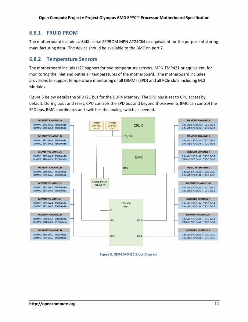
6.8.1 FRUID PROM
The motherboard includes a 64Kb serial EEPROM MPN AT24C64 or equivalent for the purpose of storing
manufacturing data. The device should be available to the BMC on port 7.
6.8.2 Temperature Sensors
The motherboard includes I2C support for two temperature sensors, MPN TMP421 or equivalent, for
monitoring the inlet and outlet air temperatures of the motherboard. The motherboard includes
provisions to support temperature monitoring of all DIMMs (SPD) and all PCIe slots including M.2
Modules.
Figure 5 below details the SPD I2C bus for the DDR4 Memory. The SPD bus is set to CPU access by
default. During boot and reset, CPU controls the SPD bus and beyond those events BMC can control the
SPD bus. BMC coordinates and switches the analog switch as needed.
Figure 5. DDR4 SPD I2C Block Diagram
CPU 0
LTC43060x94
I2C1
I2C2
I2C3
I2C4
DIMM1: SPD 0xA4 : TSOD 0x34DIMM2: SPD 0xA6 : TSOD 0x36
MEMORY CHANNEL B
DIMM1: SPD 0xA0 : TSOD 0x30DIMM2: SPD 0xA2 : TSOD 0x32
MEMORY CHANNEL A
MEMORY CHANNEL C
DIMM1: SPD 0xA8 : TSOD 0x38DIMM2: SPD 0xAA : TSOD 0x3A
DIMM1: SPD 0xAC : TSOD 0x3CDIMM2: SPD 0xAE : TSOD 0x3E
MEMORY CHANNEL D
MEMORY CHANNEL E
MEMORY CHANNEL F
MEMORY CHANNEL G
MEMORY CHANNEL H
DIMM1: SPD 0xA0 : TSOD 0x30DIMM2: SPD 0xA2 : TSOD 0x32
MEMORY CHANNEL I
DIMM1: SPD 0xA4 : TSOD 0x34DIMM2: SPD 0xA6 : TSOD 0x36
MEMORY CHANNEL J
MEMORY CHANNEL K
DIMM1: SPD 0xA8 : TSOD 0x38DIMM2: SPD 0xAA : TSOD 0x3A
DIMM1: SPD 0xAC : TSOD 0x3CDIMM2: SPD 0xAE : TSOD 0x3E
MEMORY CHANNEL L
MEMORY CHANNEL M
MEMORY CHANNEL N
MEMORY CHANNEL O
MEMORY CHANNEL P
IN
DIMM1: SPD 0xA0 : TSOD 0x30DIMM2: SPD 0xA2 : TSOD 0x32
DIMM1: SPD 0xA4 : TSOD 0x34DIMM2: SPD 0xA6 : TSOD 0x36
DIMM1: SPD 0xA8 : TSOD 0x38DIMM2: SPD 0xAA : TSOD 0x3A
DIMM1: SPD 0xAC : TSOD 0x3CDIMM2: SPD 0xAE : TSOD 0x3E
DIMM1: SPD 0xA0 : TSOD 0x30DIMM2: SPD 0xA2 : TSOD 0x32
DIMM1: SPD 0xA4 : TSOD 0x34DIMM2: SPD 0xA6 : TSOD 0x36
DIMM1: SPD 0xA8 : TSOD 0x38DIMM2: SPD 0xAA : TSOD 0x3A
DIMM1: SPD 0xAC : TSOD 0x3CDIMM2: SPD 0xAE : TSOD 0x3E
LTC2629DDR VREF
0x62
I2C2/SPD
BMC
I2C5
Analog SwitchPI3B3257A
LTC2629DDR VREF
0x20

12 November 1, 2017
6.8.3 PCIe Devices
The motherboard includes I2C support for all PCIe devices including PCIe Slots and M.2 Modules.
Communication is managed through TCA9548 (or equivalent) I2C switches to ensure that devices with
the same I2C address are supported from a single I2C port on the BMC.
6.8.4 Voltage Regulators
The motherboard includes I2C support for all the CPU and Memory Subsystem voltage regulators
enabling the BMC to monitor health of the individual power rails.
6.8.5 Hot Swap Controllers
The motherboard includes I2C support for up to two SN1402039 hot swap controllers for power
monitoring and power capping. Power is monitored by the BMC as part of the power capping function.
Accuracy of the SN1402039 is +/-0.7%.
6.8.6 Clock Buffers
There are five PCIe clock buffers on the motherboard. These clock buffers fan out the PCIe clocks for the
PCIe devices listed in section 5.3.1.These clock buffers are controlled through CPU0 I2C port0 and port1.
Figure 7 above shows generic clock devices.
6.9 JTAG
The motherboard supports muxing of the JTAG master on the BMC to support multiple uses as follows.
• Programming of the primary CPLD
• Programming of PCIe Cards (FPGA) located in Slot #4
• Exposure of HDT capabilities to the BMC
A block diagram of logical concept is shown in Figure 8.

Open Compute Project • Project Olympus AMD EPYC™ Processor Motherboard Specification
http://opencompute.org 13
Figure 6. JTAG Block Diagram
6.10 Jumpers
The design supports the jumpers listed in Table 6.
Table 3. Jumpers
Jumper Name REF Des
Status Function
BMC Disable (default) JP18 1-2 Normal (default) 2-3 Hold BMC in Reset
Disables BMC (sets all pins to High impedance)
BIOS USB Recovery JP12 1-2 BIOS USB flash recovery mode 2-3 Normal (default)
Enables BIOS recovery via USB image update
Clear CMOS JP3 1-2 Normal (default) 2-3 Clear RTC registers
Clears CMOS
Password Clear JP11 1-2 Normal (default) 2-3 Password clear
Clears the password
6.11 LEDs
The following sections describe the light-emitting diodes (LEDs) used as indicators on the motherboard.
Table 4 lists the minimum LEDs required and provides a brief description. Greater detail for some LEDs is
PCIE SLOT #4
BMCAST2520/AST2500
JTAGMASTER
CPLD
JTAGSLAVE
FPGA
JTAGSLAVE
MUX
GPIO
SEL
HDT
JTAG
PWROK
RESET_L
GPIO
GPIO
GPIO
CPU0
JTAG
DBREQ_L
DBREQ_L
CPU01
JTAG
DBREQ_L
MUX
SEL
GPIO

14 November 1, 2017
included in subsequent sections below. The visible diameter, color (λ) and brightness requirements of
the LEDs are TBD. All LEDs are visible at the front of the motherboard (cold aisle).
Table 4. LEDs
LED Name Color Description UID LED Blue Unit Identification LED
Attention LED Red Indicates that Server requires servicing
Power Status LED Amber/Green Indicates Power Status of the motherboard
SATA HDD Activity Green Indicates R/W activity to HDDs
Post Code Green Indicates the Boot status of the motherboard (Port 80)
GbE Port 0 Activity Green Indicates activity on 10GbE Port 0 (not supported for production)
GbE Port 0 Speed Green/Orange Green=high speed, Orange=Low speed (not supported for production)
PSU1 Status LED Green/Amber Status LED for PSU1
• Solid Green = AC and DC Power Good
• Blinking Green = Battery Power Good
• Solid Amber = Failure of PSU Phase
• Blinking Amber = Failure of 2 PSU Phases
PSU2 Status LED Green/Amber Status LED for PSU2 (Optional)
• Solid Green = AC and DC Power Good
• Blinking Green = Battery Power Good
• Solid Amber = Failure of PSU Phase
• Blinking Amber = Failure of 2 PSU Phases
P5V Stby LED Green Indicates 5V Standby power is present
P12V Aux LED Green Indicates 12V Auxiliary power is present
Bootup LED Green Indicates system firmware boot up
BMC Heartbeat Green Blinks to indicate BMC is alive
Alert LED Red Indicates errors occur on the motherboard
6.11.1 UID LED
The motherboard supports a blue UID (unit ID) LED used to help visually locate a specific server within a
datacenter.
6.11.2 Power Status LED
When a server is first inserted, the Power Status LED turns amber if 12V is present at the output of the
hot swap controller. This assures that the 12V power is connected and present at the motherboard and
that the hot swap controller is enabled.
When the server management software turns on the system power (CPU/Memory/PCIe), the Power
Status LED turns green. Note that the power status LED may be driven by an analog resistor network
tied directly to a power rail and is not an indication of the health of the server. Table 5 describes the
operation of the Power Status LED.
Table 5. Server Power Status LED Description
LED status Condition
Off 12V power is absent or Blade_EN# is de-asserted
Solid Amber ON Blade_EN# is asserted, 12V power output from the Hot Swap Controller is present.
Open Compute Project • Project Olympus AMD EPYC™ Processor Motherboard Specification
http://opencompute.org 15
Solid Green ON Indicates that the management (BMC) is booted and system power is enabled (CPU/Memory/PCIe).
6.11.3 Attention LED
The attention LED directs the service technicians to the server that requires service. When possible,
server diagnostics are used to direct repairs. The attention LED is driven by a single BMC GPIO. Table 9
describes the operation of the attention LED.
Table 6. Attention LED Description
LED status Condition
Off No attention indicated
Solid RED System needs attention
6.11.4 PSU Status LEDs
The motherboard supports four PSU status LEDs (2 per PSU). Each PSU is comprised of 2 individual
status LEDs indicating the PSU status as shown in Table 4. These LEDs support the WCS P2010 PSU.
Standard PSUs may not support external LEDs.
6.12 Fan Control
The motherboard supports control of twelve 40mm fans located at the rear of the server assembly. Fan
control is divided between two connectors enabling two separate fan zones. Each connector supports
12V power, a single PWM, and six TACH signals for controlling up to 6 fans in a single zone.
7 Power Management
The motherboard provides a rear connector for interfacing the motherboard to a 12V PSU. The
motherboard also provides a separate rear management connector for enabling external control of
server power. A block diagram of the interface is shown in Figure 7.

16 November 1, 2017
Figure 7. Rack Interface Block Diagram
7.1 Rack Management
The motherboard supports server control through the PMDU. The following describes the management
interfaces.
• PWR_EN# - Active low signal used to enable/disable power to the P2010 PSU. A 1K ohm pulldown resistor is used on the motherboard to ensure a default low state (active) if the Rack Manager is not present. This signal connects to the PS_ON# signal of the PSU. When in high state (inactive), this signal disables output power from the P2010 PSU.
• SERVER_PRESENT# - Active low signal used to communicate physical presence of the server to the Rack Manager. This signal should be tied to GND on the motherboard.
• SERVER_THROTTLE - Active high signal used to put the motherboard into a low power (power cap) state. This signal should default low (inactive) if the Rack Manager is not present. This signal is fanned out from the Rack Manager to multiple servers and therefore the circuit design must support electrical isolation of this signal from the motherboard power planes.
• SLOT_ID[5:0] – Identifies the physical rack slot in which the server is installed. ID is hard set by the PMDU. The ID decoding is shown below in Table 7.
LR_SELECT – Spare signal. Used to differentiate between left and right slots for a dual-node
implementation.
Table 7. Slot ID Decode
Slot SLOT_ID[5:0] Slot SLOT_ID[5:0]
Slot 1 000000 Slot 25 100000
Slot 2 000001 Slot 26 100001

Open Compute Project • Project Olympus AMD EPYC™ Processor Motherboard Specification
http://opencompute.org 17
Slot 3 000010 Slot 27 100010
Slot 4 000011 Slot 28 100011
Slot 5 000100 Slot 29 100100
Slot 6 000101 Slot 30 100101
Slot 7 001000 Slot 31 101000
Slot 8 001001 Slot 32 101001
Slot 9 001010 Slot 33 101010
Slot 10 001011 Slot 34 101011
Slot 11 001100 Slot 35 101100
Slot 12 001101 Slot 36 101101
Slot 13 010000 Slot 37 110000
Slot 14 010001 Slot 38 110001
Slot 15 010010 Slot 39 110010
Slot 16 010011 Slot 40 110011
Slot 17 010100 Slot 41 110100
Slot 18 010101 Slot 42 110101
Slot 19 011000 Slot 43 111000
Slot 20 011001 Slot 44 111001
Slot 21 011010 Slot 45 111010
Slot 22 011011 Slot 46 111011
Slot 23 011100 Slot 47 111100
Slot 24 011101 Slot 48 111101
7.2 PSU Management
The motherboard supports management of the P2010 PSU through a management cable. Below is a
description of the signals supported by PMDU.
• PS_ON# - Active low signal used to enable/disable power to the PSU. This signal is driven by the
PWR_EN# signal from Rack Manager. A 1K ohm pulldown resistor is used on the motherboard to
ensure a default low state if the RM is not present.
• PSU_ALERT# - Active low signal used to alert the motherboard that a fault has occurred in the
PSU. Assertion of this signal by the PSU puts the motherboard into a low power (PROCHOT)
state. This signal is also connected to the BMC for monitoring PSU status.
• PMBUS – I2C interface to the PSU. This is used by the BMC to read status of the PSU.
• STATUS_LED – Controls LED to provide visual indication of a PSU fault.

18 November 1, 2017
7.3 Hot Swap Controller
The motherboard supports a hot swap controller (HSC), MPN SN1402039, for in-rush current protection
and power monitoring. The HSC includes support for the PMBUS interface. The hot swap controller
disables 12V to the motherboard over PSU overcurrent limit 72A.
7.4 Power Capping
The motherboard supports throttling of the processors using the Fast PROCHOT mechanism based on
monitoring of the motherboards input voltage and power. A block diagram detailing these triggers is
shown in Figure 8.
The following triggers are monitored by the BMC and can directly generate PROCHOT# events. Each
trigger is filtered by the CPLD. The CPLD ensures that any event trigger will generate a minimum 100ms
PROCHOT# pulse.
• Undervoltage – A comparator monitors the 12V output of the HSC and asserts if this voltage falls
below 11.5V.
• Overcurrent Alert – The HSC monitors the input current and asserts the trigger if the input
current exceeds 65A.
• Overcurrent Protect – The HSC monitors the input current and disables power to the
motherboard if the current exceeds 72A.
• HSC ALERT #1 and #2 – The HSC provides two programmable alerts. These alerts are spare
inputs and will be disabled by default.
Note that the CPU voltage regulators also can generate PROCHOT triggers to the CPUs.
The motherboard enables power capping of the server from different trigger sources. Assertion of
either of the following causes the motherboard to assert PROCHOT and the CPLD to initiate power
capping of the server.
• RM THROTTLE# - Throttle signal driven by the Rack Manager indicating that the rack has
exceeded its power limit.
• PSU ALERT# - Alert signal driven by the PSU. Assertion indicates an over-current event or that
the Olympus PSU has transitioned its power source from AC to battery backup.
• FM_THROTTLE# - Test signal that allows BMC to assert power cap

Open Compute Project • Project Olympus AMD EPYC™ Processor Motherboard Specification
http://opencompute.org 19
Figure 8. PROCHOT Block Diagram
7.5 PWRBRK#
The motherboard supports Emergency Power Reduction mechanism (PWRBRK#) for the x16 PCIe slots.
The primary purpose is to provide a power reduction mechanism for GPGPU cards as part of the throttle
and power capping strategy. Figure 9 shows the block diagram for PWRBRK#. PWRBRK# can be
triggered by either the RM_THROTTLE# or PSU2_ALERT#. Logic for PWRBRK# is contained in the CPLD.
The BMC controls enable/disable monitoring of the two triggers and can also force an event.
Figure 9. PWRBRK# Block Diagram
7.6 MEM VRHOT and EVENT_L
The motherboard supports memory thermal event mitigation feature. Each channel of CPU memory
controller has a dedicated input for DIMM EVENT_L signals. All DIMM EVENT_L signals are connected to
CPUs. CPU can be configured to place DIMM into 2x refresh mode or activating throttling. All EVENT_L
signals are also routed to CPLD and BMC can either poll the status through I2C bus or CPLD can generate
BMC
12VOC Monitor
60A
CPLD12VUV Monitor
11.5V
FAST PROCHOT Triggers
100msPulse Gen
CPU0PWRINALERT#
CPU0 VRPVCCIN VRHOT
CPU1PWRINALERT#
CPU1 VRPVCCIN VRHOT
FM_NM_THROTTLE#
VR PROCHOT Triggers
RMTHROTTLE#
RM_THROTTLE_EN#
PMB_ALERT_EN#
RM_THROTTLE#
PMB_ALERT#
PSU PMBUSALERT#
HSC_ALERT2#
HSCALERT#1
HSCALERT#2
HSC_ALERT1#
OC_DETECT#
Power Cap Triggers
FM_THROTTLE_IN#
UV_ALERT#
RM_THROTTLE# (SPARE)
PSU_ALRT# (SPARE)
SPARE
SPARE
CPU1
CPU0
PROCHOT#
PROCHOT#
OD
OD
SOC0PWRINALERT#
SOC0 VRPVCCIN VRHOT
SOC1PWRINALERT#
SOC1 VRPVCCIN VRHOT

20 November 1, 2017
a trigger through a GPIO to BMC. All MEM VRHOT signals are routed to BMC GPIOs. BMC will log any
memory VRHOT and EVENT_L events. A SPARE signal is reserved from BMC to CPLD for MEM VRHOT
indication for future implementation. The block diagrams of MEM VRHOT and EVENT_L are shown
below.
Figure 10. MEM VRHOT Block Diagram
Figure 11. MEM EVENT_L Block Diagram
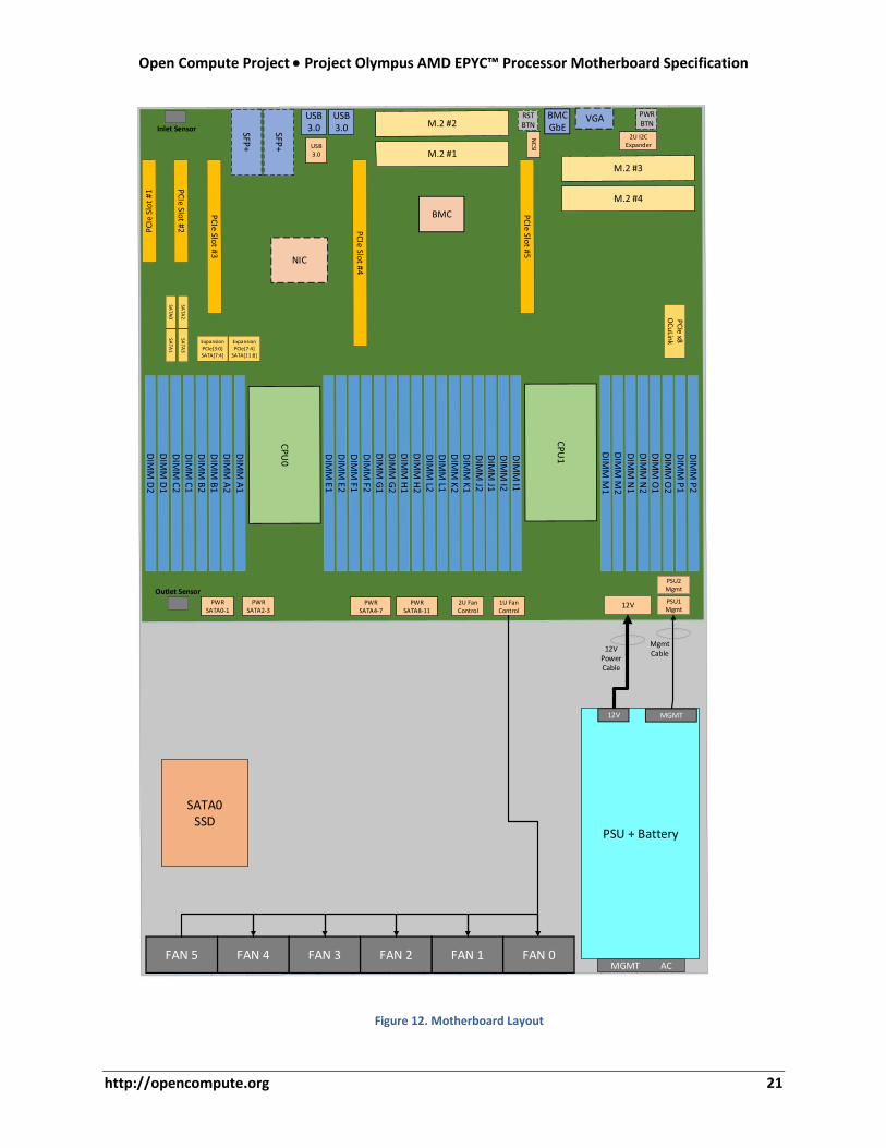
8 Motherboard Layout
Figure 12 shows a representative layout of the motherboard with approximate locations of major
components and connectors.
MEM IJKLVRHot
MEM MNOPVRHot
MEM ABCDVRHot
MEM EFGHVRHot
BMC
VRHOT ABCD
VRHOT EFGH
VRHOT IJKL
VRHOT MNOP
CPLD
SPARESPARE
DIMM Channel B EVENT_L
DIMM Channel A EVENT_L
DIMM Channel F EVENT_L
DIMM Channel E EVENT_L CPU0
MA_EVENT_L
DIMM Channel D EVENT_L
DIMM Channel C EVENT_L
DIMM Channel H EVENT_L
DIMM Channel G EVENT_L
MB_EVENT_L
MC_EVENT_L
MD_EVENT_L
ME_EVENT_L
MF_EVENT_L
MG_EVENT_L
MH_EVENT_L
CPLD
DIMM Channel J EVENT_L
DIMM Channel I EVENT_L
DIMM Channel N EVENT_L
DIMM Channel M EVENT_L CPU1
MA_EVENT_L
DIMM Channel L EVENT_L
DIMM Channel K EVENT_L
DIMM Channel P EVENT_L
DIMM Channel O EVENT_L
MB_EVENT_L
MC_EVENT_L
MD_EVENT_L
ME_EVENT_L
MF_EVENT_L
MG_EVENT_L
MH_EVENT_L
BMC
SPARESPARE
GPIOs I2C[5]
EVENT_N ABCD
EVENT_N EFGH
EVENT_N IJKL
EVENT_N MNOP
Open Compute Project • Project Olympus AMD EPYC™ Processor Motherboard Specification
http://opencompute.org 21
Figure 12. Motherboard Layout
BMC
12V
Inlet Sensor
Outlet Sensor
ExpansionPCIe[7:4]
SATA[11:8]
USB3.0
NIC
MGMT AC
SATA0SSD
PSU + Battery
12VPowerCable
PSU1Mgmt
MgmtCable
USB3.0
ExpansionPCIe[3:0]SATA[7:4]
SATA
2
SATA
0
PSU2Mgmt
12V MGMT
PC
Ie x8
OC
uLin
k
BMCGbE
VGA
1U Fan Control
2U Fan Control
FAN 0FAN 1FAN 2FAN 3FAN 4FAN 5
PWRSATA2-3
PWRSATA0-1
USB3.0
SATA
3
SATA
1
PWRSATA4-7
PWRSATA8-11
2U I2CExpander
NC
SI
RSTBTN
PWRBTN

22 November 1, 2017
9 Serviceability
9.1 Debug features
The following minimum debug features are supported on the motherboard:
• I2C Debug headers on all I2C ports. Header shall be a 3-pin compatible with standard I2C
Protocol Analyzers such as Beagle or Aardvark.
• Debug connectors on all UARTs, 4-pin 2.54mm headers.
• POST LEDs.
• BIOS Debug Support Including:
o Two socketed BIOS Flash (socket to be removed for production)
o BIOS recovery jumper connected to CPU GPIO
• HDT Header contains both the JTAG and Debug signals. This connector is for interfacing to HDT
tool to control and monitor the processor.
• Two USB 3.0 ports connected to CPU0 USB0 Port 0 and Port 1. The connectors are Type A and
the location is at the front of the motherboard for support of servicing at the front of the server
assembly. All external USB Ports are capable of operating at USB 3.0, 2.0, or 1.0.
• Two USB 2.0 connections from BMC to CPU.
• BMC disable jumper is attached to GPIO on BMC. The motherboard supports BIOS setting to
enable autoboot of motherboard in the event the BMC is disabled.
• CPU Recovery Mode Jumper
• HW jumper to enable BIOS serial debug output
9.2 LED Visibility
Motherboard LEDs determined to be important for communicating status to service personnel are
visible at the front (cold aisle) of the motherboard.
• UID LED
• Power Status LED
• Attention LED
10 Motherboard Interfaces
This section describes the connector interfaces to the motherboard.

Open Compute Project • Project Olympus AMD EPYC™ Processor Motherboard Specification
http://opencompute.org 23
10.1 PCIe x8 Connectors
The PCIe x8 connector interfaces are designed to support a standard PCIe x8 card as well as the M.2 riser
card. The M.2 riser card is a custom edge card PCA that supports two M.2 SSD Modules (NGFF form
factor cards) in the SSD Socket 3 format per the PCI Express M.2 Specification. To support two M.2
modules, the PCIe connector interface is altered to support 2 PCIe Gen3 x4 interfaces as well as the SSD
specific signals per the PCIE M.2 specification. Table 12 describes the connector pinout. The signals
satisfy the electrical requirements of the PCIE Card Electromechanical Specification. The following is a
list of pin assignment deviations from that specification needed to support two M.2 modules. These
signals are highlighted in red.
• SUSCLK is assigned to pin A6 replacing JTAG TDI pin. Support for SUSCLK is not required.
• LINKWIDTH is assigned to pin B17 replacing PRSNT#2. Enables auto-detection of 2x4 M.2
Interposer or 1x8 standard PCIe card. The design is not required to support PCIe x1 cards.
• REFCLK2+/- is assigned to pins A32/A33 replacing two Reserved pins.
• SMBCLK2 and SMBDAT2 are assigned to pins A7/A8 replacing TDO and TMS pins.
Table 8. PCIe x8 connector pinout
Pin Side B Connector Side A Connector
# Name Description Name Description
1 +12v +12 volt power PRSNT#1 Hot plug presence detect
2 +12v +12 volt power +12v +12 volt power
3 +12v +12 volt power +12v +12 volt power
4 GND Ground GND Ground
5 SMCLK1 SMBus clock JTAG2 TCK
6 SMDAT1 SMBus data SUSCLK Suspend Clk
7 GND Ground SMCLK2 SMBus clock
8 +3.3v +3.3 volt power SMDAT2 SMBus data
9 JTAG1 +TRST# +3.3v +3.3 volt power
10 3.3Vaux 3.3v volt power +3.3v +3.3 volt power
11 WAKE# Link Reactivation PGOOD Powergood
Mechanical Key
12 CLKREQ# Request Running Clock
GND Ground
13 GND Ground REFCLK1+ Reference Clock
14 PETP(0) Transmitter Lane 0, REFCLK1- Differential pair
15 PETN(0) Differential pair GND Ground
16 GND Ground PERP(0) Receiver Lane 0,
17 LINKWIDTH 0= 2 x4 PERN(0) Differential pair

24 November 1, 2017
1= 1 x8
18 GND Ground GND Ground
19 PETP(1) Transmitter Lane 1, RSVD Reserved
20 PETN(1) Differential pair GND Ground
21 GND Ground PERP(1) Receiver Lane 1,
22 GND Ground PERN(1) Differential pair
23 PETP(2) Transmitter Lane 2, GND Ground
24 PETN(2) Differential pair GND Ground
25 GND Ground PERP(2) Receiver Lane 2,
26 GND Ground PERN(2) Differential pair
27 PETP(3) Transmitter Lane 3, GND Ground
28 PETN(3) Differential pair GND Ground
29 GND Ground PERP(3) Receiver Lane 3,
30 RSVD Reserved PERN(3) Differential pair
31 PRSNT#2 Presence Detect GND Ground
32 GND Ground REFCLK2+ Reference Clock Differential pair 33 PETP(4) Transmitter Lane 4, REFCLK2-
34 PETN(4) Differential pair GND Ground
35 GND Ground PERP(4) Receiver Lane 4,
36 GND Ground PERN(4) Differential pair
37 PETP(5) Transmitter Lane 5, GND Ground
38 PETN(5) Differential pair GND Ground
39 GND Ground PERP(5) Receiver Lane 5,
40 GND Ground PERN(5) Differential pair
41 PETP(6) Transmitter Lane 6, GND Ground
42 PETN(6) Differential pair GND Ground
43 GND Ground PERP(6) Receiver Lane 6,
44 GND Ground PERN(6) Differential pair
45 PETP(7) Transmitter Lane 7, GND Ground
46 PETN(7) Differential pair GND Ground
47 GND Ground PERP(7) Receiver Lane 7,
48 PRSNT#2 Presence detect PERN(7) Differential pair
49 GND Ground GND Ground

Open Compute Project • Project Olympus AMD EPYC™ Processor Motherboard Specification
http://opencompute.org 25
10.2 PCIe x16 Connectors
The PCIe x16 connector interface is designed to support a standard PCIe x16 full height card. The pinout
for supporting PCIe x16 described in Table 13. This interface also supports the PWRBRK# power
reduction feature. Note that this signal is declared on pins B12 and B30. This enables support for this
feature on existing platforms (B12) and meets the latest PCI SIG definition (B30). For further
information, refer to the PCI Express® Card Electromechanical Specification.
Table 9. PCIe x16 connector pinout
Pin Side B Connector Side A Connector
# Name Description Name Description
1 +12v +12 volt power PRSNT#1 Hot plug presence detect
2 +12v +12 volt power +12v +12 volt power
3 +12v +12 volt power +12v +12 volt power
4 GND Ground GND Ground
5 SMCLK SMBus clock JTAG2 TCK
6 SMDAT SMBus data JTAG3 TDI
7 GND Ground JTAG4 TDO
8 +3.3v +3.3 volt power JTAG5 TMS
9 JTAG1 +TRST# +3.3v +3.3 volt power
10 3.3Vaux 3.3v volt power +3.3v +3.3 volt power
11 WAKE# Link Reactivation PWRGD Power Good
Mechanical Key
12 PWRBRK# Power Reduction GND Ground
13 GND Ground REFCLK+ Reference Clock
14 PETP(0) Transmitter Lane 0, REFCLK- Differential pair
15 PETN(0) Differential pair GND Ground
16 GND Ground PERP(0) Receiver Lane 0,
17 PRSNT#2 Presence detect PERN(0) Differential pair
18 GND Ground GND Ground
19 PETP(1) Transmitter Lane 1, RSVD Reserved
20 PETN(1) Differential pair GND Ground
21 GND Ground PERP(1) Receiver Lane 1,
22 GND Ground PERN(1) Differential pair
23 PETP(2) Transmitter Lane 2, GND Ground
24 PETN(2) Differential pair GND Ground
25 GND Ground PERP(2) Receiver Lane 2,

26 November 1, 2017
26 GND Ground PERN(2) Differential pair
27 PETP(3) Transmitter Lane 3, GND Ground
28 PETN(3) Differential pair GND Ground
29 GND Ground PERP(3) Receiver Lane 3,
30 PWRBRK# Power Reduction PERN(3) Differential pair
31 PRSNT#2 Hot plug detect GND Ground
32 GND Ground RSVD Reserved
33 PETP(4) Transmitter Lane 4, RSVD Reserved
34 PETN(4) Differential pair GND Ground
35 GND Ground PERP(4) Receiver Lane 4,
36 GND Ground PERN(4) Differential pair
37 PETP(5) Transmitter Lane 5, GND Ground
38 PETN(5) Differential pair GND Ground
39 GND Ground PERP(5) Receiver Lane 5,
40 GND Ground PERN(5) Differential pair
41 PETP(6) Transmitter Lane 6, GND Ground
42 PETN(6) Differential pair GND Ground
43 GND Ground PERP(6) Receiver Lane 6,
44 GND Ground PERN(6) Differential pair
45 PETP(7) Transmitter Lane 7, GND Ground
46 PETN(7) Differential pair GND Ground
47 GND Ground PERP(7) Receiver Lane 7,
48 PRSNT#2 Hot plug detect PERN(7) Differential pair
49 GND Ground GND Ground
50 PETP(8) Transmitter Lane 8, RSVD Reserved
51 PETN(8) Differential pair GND Ground
52 GND Ground PERP(8) Receiver Lane 8,
53 GND Ground PERN(8) Differential pair
54 PETP(9) Transmitter Lane 9, GND Ground
55 PETN(9) Differential pair GND Ground
56 GND Ground PERP(9) Receiver Lane 9,
57 GND Ground PERN(9) Differential pair
58 PETP(10) Transmitter Lane 10, GND Ground
59 PETN(10) Differential pair GND Ground
60 GND Ground PERP(10) Receiver Lane 10,
61 GND Ground PERN(10) Differential pair
Open Compute Project • Project Olympus AMD EPYC™ Processor Motherboard Specification
http://opencompute.org 27
62 PETP(11) Transmitter Lane 11, GND Ground
63 PETN(11) Differential pair GND Ground
64 GND Ground PERP(11) Receiver Lane 11,
65 GND Ground PERN(11) Differential pair
66 PETP(12) Transmitter Lane 12, GND Ground
67 PETN(12) Differential pair GND Ground
68 GND Ground PERP(12) Receiver Lane 12,
69 GND Ground PERN(12) Differential pair
70 PETP(13) Transmitter Lane 13, GND Ground
71 PETN(13) Differential pair GND Ground
72 GND Ground PERP(13) Receiver Lane 13,
73 GND Ground PERN(13) Differential pair
74 PETP(14) Transmitter Lane 14, GND Ground
75 PETN(14) Differential pair GND Ground
76 GND Ground PERP(14) Receiver Lane 14,
77 GND Ground PERN(14) Differential pair
78 PETP(15) Transmitter Lane 15, GND Ground
79 PETN(15) Differential pair GND Ground
80 GND Ground PERP(15) Receiver Lane 15,
81 PRSNT#2 Hot plug present detect PERN(15) Differential pair
82 RSVD#2 Hot Plug Detect GND Ground
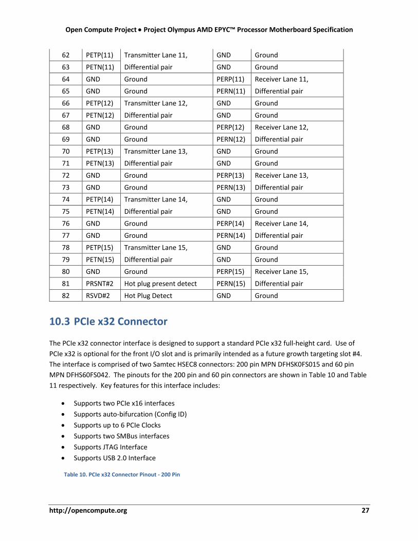
10.3 PCIe x32 Connector
The PCIe x32 connector interface is designed to support a standard PCIe x32 full-height card. Use of
PCIe x32 is optional for the front I/O slot and is primarily intended as a future growth targeting slot #4.
The interface is comprised of two Samtec HSEC8 connectors: 200 pin MPN DFHSK0FS015 and 60 pin
MPN DFHS60FS042. The pinouts for the 200 pin and 60 pin connectors are shown in Table 10 and Table
11 respectively. Key features for this interface includes:
• Supports two PCIe x16 interfaces
• Supports auto-bifurcation (Config ID)
• Supports up to 6 PCIe Clocks
• Supports two SMBus interfaces
• Supports JTAG Interface
• Supports USB 2.0 Interface
Table 10. PCIe x32 Connector Pinout - 200 Pin

28 November 1, 2017
Pin Side A Connector Side B Connector Pin
# Name Description Name Description #
1 P12V +12 volt power P12V +12 volt power 2
3 P12V +12 volt power P12V +12 volt power 4
5 P12V +12 volt power P12V +12 volt power 6
7 P12V +12 volt power P12V +12 volt power 8
9 P12V +12 volt power P12V +12 volt power 10
11 P12V +12 volt power P12V +12 volt power 12
13 GND Ground GND Ground 14
15 BMC_SMBDAT SMBus to BMC BMC_ALERT# SMBus Alert to BMC 16
17 BMC_SMCLK SMBus to BMC SLT_CFG1 Slot Configuration Bit1 18
19 SLT_CFG0 Slot Configuration Bit0 PWRBREAK# Power Break 20
21 P3V3 +3.3 volt power P3V3 +3.3 volt power 22
23 P3V3 +3.3 volt power P3V3 +3.3 volt power 24
25 P3V3_STBY +3.3 volt stby power GND Ground 26
27 CPU_ALERT# SMBus Alert to CPU WAKE# Wake 28
29 PERST# PCIe Reset CPU_SMDAT SMBus to CPU 30
31 GND Ground CPU_SMCLK SMBus to CPU 32
33 CLK_100M_DP<0> Reference Clock GND Ground 34
35 CLK_100M_DN<0> Differential pair CLK_100M_DP<1> Reference Clock 36
37 GND Ground CLK_100M_DN<1> Differential pair 38
39 CLK_100M_DP<2> Reference Clock GND Ground 40
41 CLK_100M_DN<2> Differential pair CLK_100M_DP<3> Reference Clock 42
43 GND Ground CLK_100M_DN<3> Differential pair 44
45 CLK_100M_DP<4> Reference Clock GND Ground 46
47 CLK_100M_DN<4> Differential pair CLK_100M_DP<5> Reference Clock 48
49 GND Ground CLK_100M_DN<5> Differential pair 50
51 P3E_P0_TXP<15> Transmitter Lane 15, GND Ground 52
53 P3E_P0_TXN<15> Differential pair P3E_P0_RXP<15> Receiver Lane 15, 54
55 GND Ground P3E_P0_RXN<15> Differential pair 56
57 P3E_P0_TXP<14> Transmitter Lane 14, GND Ground 58
59 P3E_P0_TXN<14> Differential pair P3E_P0_RXN<14> Receiver Lane 14, 60
61 GND Ground P3E_P0_RXP<14> Differential pair 62
63 RSVD1 Reserved GND Ground 64
65 GND Ground RSVD2 Reserved 66
67 P3E_P0_TXN<13> Transmitter Lane 13, GND Ground 68
69 P3E_P0_TXP<13> Differential pair P3E_P0_RXP<13> Receiver Lane 13, 70
71 GND Ground P3E_P0_RXN<13> Differential pair 72
73 P3E_P0_TXN<12> Transmitter Lane 12, GND Ground 74
75 P3E_P0_TXP<12> Differential pair P3E_P0_RXP<12> Receiver Lane 12, 76
77 GND Ground P3E_P0_RXN<12> Differential pair 78
79 P3E_P0_TXN<11> Transmitter Lane 11, GND Ground 80
81 P3E_P0_TXP<11> Differential pair P3E_P0_RXP<11> Receiver Lane 11, 82
83 GND Ground P3E_P0_RXN<11> Differential pair 84
85 P3E_P0_TXN<10> Transmitter Lane 10, GND Ground 86
Open Compute Project • Project Olympus AMD EPYC™ Processor Motherboard Specification
http://opencompute.org 29
87 P3E_P0_TXP<10> Differential pair P3E_P0_RXP<10> Receiver Lane 10, 88
89 GND Ground P3E_P0_RXN<10> Differential pair 90
91 P3E_P0_TXP<9> Transmitter Lane 9, GND Ground 92
93 P3E_P0_TXN<9> Differential pair P3E_P0_RXP<9> Receiver Lane 9, 94
95 GND Ground P3E_P0_RXN<9> Differential pair 96
97 P3E_P0_TXP<8> Transmitter Lane 8, GND Ground 98
99 P3E_P0_TXN<8> Differential pair P3E_P0_RXP<8> Receiver Lane 8, 100
101 GND Ground P3E_P0_RXN<8> Differential pair 102
103 P3E_P0_TXP<7> Transmitter Lane 7, GND Ground 104
105 P3E_P0_TXN<7> Differential pair P3E_P0_RXP<7> Receiver Lane 7, 106
107 GND Ground P3E_P0_RXN<7> Differential pair 108
109 P3E_P0_TXP<6> Transmitter Lane 6, GND Ground 110
111 P3E_P0_TXN<6> Differential pair P3E_P0_RXP<6> Receiver Lane 6, 112
113 GND Ground P3E_P0_RXN<6> Differential pair 114
115 P3E_P0_TXP<5> Transmitter Lane 5, GND Ground 116
117 P3E_P0_TXN<5> Differential pair P3E_P0_RXP<5> Receiver Lane 5, 118
119 GND Ground P3E_P0_RXN<5> Differential pair 120
121 P3E_P0_TXP<4> Transmitter Lane 4, GND Ground 122
123 P3E_P0_TXN<4> Differential pair P3E_P0_RXP<4> Receiver Lane 4, 124
125 GND Ground P3E_P0_RXN<4> Differential pair 126
127 P3E_P0_TXP<3> Transmitter Lane 3, GND Ground 128
129 P3E_P0_TXN<3> Differential pair P3E_P0_RXP<3> Receiver Lane 3, 130
131 GND Ground P3E_P0_RXN<3> Differential pair 132
133 P3E_P0_TXP<2> Transmitter Lane 2, GND Ground 134
135 P3E_P0_TXN<2> Differential pair P3E_P0_RXP<2> Receiver Lane 2, 136
137 GND Ground P3E_P0_RXN<2> Differential pair 138
139 P3E_P0_TXP<1> Transmitter Lane 1, GND Ground 140
141 P3E_P0_TXN<1> Differential pair P3E_P0_RXP<1> Receiver Lane 1, 142
143 GND Ground P3E_P0_RXN<1> Differential pair 144
145 P3E_P0_TXP<0> Transmitter Lane 0, GND Ground 146
147 P3E_P0_TXN<0> Differential pair P3E_P0_RXP<0> Receiver Lane 0, 148
149 GND Ground P3E_P0_RXN<0> Differential pair 150
151 P3E_P1_TXP<15> Transmitter Lane 15, GND Ground 152
153 P3E_P1_TXP<15> Differential pair P3E_P1_RXP<15> Receiver Lane 15, 154
155 GND Ground P3E_P1_RXP<15> Differential pair 156
157 P3E_P1_TXP<14> Transmitter Lane 14, GND Ground 158
159 P3E_P1_TXN<14> Differential pair P3E_P1_RXP<14> Receiver Lane 14, 160
161 GND Ground P3E_P1_RXN<14> Differential pair 162
163 P3E_P1_TXP<13> Transmitter Lane 13, GND Ground 164
165 P3E_P1_TXN<13> Differential pair P3E_P1_RXP<13> Receiver Lane 13, 166
167 GND Ground P3E_P1_RXN<13> Differential pair 168
169 P3E_P1_TXP<12> Transmitter Lane 12, GND Ground 170
171 P3E_P1_TXN<12> Differential pair P3E_P1_RXP<12> Receiver Lane 12, 172
173 GND Ground P3E_P1_RXN<12> Differential pair 174
175 P3E_P1_TXP<11> Transmitter Lane 11, GND Ground 176
177 P3E_P1_TXN<11> Differential pair P3E_P1_RXP<11> Receiver Lane 11, 178

30 November 1, 2017
179 GND Ground P3E_P1_RXN<11> Differential pair 180
181 P3E_P1_TXP<10> Transmitter Lane 10, GND Ground 182
183 P3E_P1_TXN<10> Differential pair P3E_P1_RXP<10> Receiver Lane 10, 184
185 GND Ground P3E_P1_RXN<10> Differential pair 186
187 P3E_P1_TXP<9> Transmitter Lane 9, GND Ground 188
189 P3E_P1_TXN<9> Differential pair P3E_P1_RXP<9> Receiver Lane 9, 190
191 GND Ground P3E_P1_RXN<9> Differential pair 192
193 P3E_P1_TXP<8> Transmitter Lane 8, GND Ground 194
195 P3E_P1_TXN<8> Differential pair P3E_P1_RXP<8> Receiver Lane 8, 196
197 GND Ground P3E_P1_RXN<8> Differential pair 198
199 PRESENT# Present signal GND Ground 200
Table 11. PCIe x32 Connector Pinout - 60 Pin
Pin Side A Golden Finger Side B Golden Finger Pin
# Name Description Name Description #
1 GND Ground RSVD2 Reserved 2
3 P3E_P1_TXP<7> Transmitter Lane 7, GND Ground 4
5 P3E_P1_TXN<7> Differential pair P3E_P1_RXP<7> Receiver Lane 7, 6
7 GND Ground P3E_P1_RXN<7> Differential pair 8
9 P3E_P1_TXP<6> Transmitter Lane 6, GND Ground 10
11 P3E_P1_TXN<6> Differential pair P3E_P1_RXP<6> Receiver Lane 6, 12
13 GND Ground P3E_P1_RXN<6> Differential pair 14
15 P3E_P1_TXP<5> Transmitter Lane 5, GND Ground 16
17 P3E_P1_TXN<5> Differential pair P3E_P1_RXP<5> Receiver Lane 5, 18
19 GND Ground P3E_P1_RXN<5> Differential pair 20
21 P3E_P1_TXP<4> Transmitter Lane 4, GND Ground 22
23 P3E_P1_TXN<4> Differential pair P3E_P1_RXP<4> Receiver Lane 4, 24
25 GND Ground P3E_P1_RXN<4> Differential pair 26
27 P3E_P1_TXP<3> Transmitter Lane 3, GND Ground 28
29 P3E_P1_TXN<3> Differential pair P3E_P1_RXP<3> Receiver Lane 3, 30
31 GND Ground P3E_P1_RXN<3> Differential pair 32
33 P3E_P1_TXP<2> Transmitter Lane 2, GND Ground 34
35 P3E_P1_TXN<2> Differential pair P3E_P1_RXP<2> Receiver Lane 2, 36
37 GND Ground P3E_P1_RXN<2> Differential pair 38
39 P3E_P1_TXP<1> Transmitter Lane 1, GND Ground 40
41 P3E_P1_TXN<1> Differential pair P3E_P1_RXP<1> Receiver Lane 1, 42
43 GND Ground P3E_P1_RXN<1> Differential pair 44
45 P3E_P1_TXP<0> Transmitter Lane 0, GND Ground 46
47 P3E_P1_TXN<0> Differential pair P3E_P1_RXP<0> Receiver Lane 0, 48
49 GND Ground P3E_P1_RXN<0> Differential pair 50
51 JTAG_TDI JTAG TDI GND Ground 52
53 JTAG_TDO JTAG TDO JTAG_TMS JTAG TMS 54
55 GND Ground JTAG_TCK JTAG TCK 56
57 USB2_DP USB 2.0 GND Ground 58

Open Compute Project • Project Olympus AMD EPYC™ Processor Motherboard Specification
http://opencompute.org 31
59 USB2_DN USB 2.0 JTAG_TRST JTAG Reset 60
10.4 PCIe MiniSAS HD Connectors
The motherboard optionally supports vertical MiniSAS HD connectors for cabling PCIe from the
motherboard to rear PCIe expansion cards. The connector supports four lanes of PCIe and the necessary
management signals (clocks, PERST#) to operate as a standalone PCIe interface.
Table 12. PCIe Cable Connector Pinout
PCIe Cable Connector Pinout
Pin Signal Description
D9 GND Ground
D8 TX2- PCIe Transmit Lane 2
D7 TX2+ PCIe Transmit Lane 2
D6 GND Ground
D5 TX0- PCIe Transmit Lane 0
D4 TX0+ PCIe Transmit Lane 0
D3 GND Ground
D2 SB6 BMC_SMB_CLK
D2 SB5 BMC_SMB_DAT
C1 NC NC
C2 NC NC
C3 GND Ground
C4 TX1+ PCIe Transmit Lane 1
C5 TX1- PCIe Transmit Lane 1
C6 GND Ground
C7 TX3+ PCIe Transmit Lane 3
C8 TX3- PCIe Transmit Lane 3
C9 GND Ground
B9 GND Ground
B8 RX2- PCIe Receive Lane 2
B7 RX2+ PCIe Receive Lane 2
B6 GND Ground
B5 RX0- PCIe Receive Lane 0
B4 RX0+ PCIe Receive Lane 0
B3 GND Ground
B2 GND GND
B1 PERST# PERST#
A1 REFCLK+ PCIe Reference Clock
A2 REFCLK- PCIe Reference Clock
A3 GND Ground

32 November 1, 2017
A4 RX1+ PCIe Receive Lane 1
A5 RX1- PCIe Receive Lane 1
A6 GND Ground
A7 RX3+ PCIe Receive Lane 3
A8 RX3- PCIe Receive Lane 3
A9 GND Ground
10.5 M.2 Connectors
M.2 connectors are integrated into the motherboard for supporting flash memory expansion. The M.2
connector pinout is shown in Table 13. For more information about the M.2 interface, refer to the PCI
Express M.2 Specification.
Table 13. M.2 connector pinout
M.2 Module Standard Pinout
Pin Signal Description Pin Signal Description
74 3.3V 3.3V Power 75 GND Ground
72 3.3V 3.3V Power 73 GND Ground
70 3.3V 3.3V Power 71 GND Ground
68 SUSCLK(32KHz) Reduce Power Clock 69 NC Reserved
66 KEY Module Key 67 GND Ground
64 KEY Module Key 65 KEY Module Key
62 KEY Module Key 63 KEY Module Key
60 KEY Module Key 61 KEY Module Key
58 NC Reserved 59 KEY Module Key
56 NC Reserved 57 GND Ground
54 PEWAKE# PCIe PME Wake (Open Drain) 55 REFLKCP PCIe Reference Clock
52 CLKREQ# Reference Clock Request 53 REFLKCN PCIe Reference Clock
50 PERST# PCIe Reset 51 GND Ground
48 NC Reserved 49 PETP0 PCIe Transmit Lane 0
46 NC Reserved 47 PETN0 PCIe Transmit Lane 0
44 ALERT# SMBus ALERT 45 GND Ground
42 SMB_DATA SMBus Data 43 PERP0 PCIe Receive Lane 0
40 SMB_CLK SMBus Clock 41 PERN0 PCIe Receive Lane 0
38 DEVSLP Device Sleep 39 GND Ground
36 NC Reserved 37 PETP1 PCIe Transmit Lane 0

Open Compute Project • Project Olympus AMD EPYC™ Processor Motherboard Specification
http://opencompute.org 33
34 NC Reserved 35 PETN1 PCIe Transmit Lane 0
32 NC Reserved 33 GND Ground
30 NC Reserved 31 PERP1 PCIe Receive Lane 0
28 NC Reserved 29 PERN1 PCIe Receive Lane 0
26 NC Reserved 27 GND Ground
24 NC Reserved 25 PETP2 PCIe Transmit Lane 0
22 NC Reserved 23 PETN2 PCIe Transmit Lane 0
20 NC Reserved 21 GND Ground
18 3.3V 3.3V Power 19 PERP2 PCIe Receive Lane 0
16 3.3V 3.3V Power 17 PERN2 PCIe Receive Lane 0
14 3.3V 3.3V Power 15 GND Ground
12 3.3V 3.3V Power 13 PETP3 PCIe Transmit Lane 0
10 DAS/DSS# Drive Active Signal (Open Drain) 11 PETN3 PCIe Transmit Lane 0
8 NC Reserved 9 GND Ground
6 NC Reserved 7 PERP3 PCIe Receive Lane 0
4 3.3V 3.3V Power 5 PERN3 PCIe Receive Lane 0
2 3.3V 3.3V Power 3 GND Ground
1 GND Ground
10.6 SATA Cable Ports
The motherboard supports four x1 SATA standard 7-pin connectors. The motherboard optionally
supports up to one x4 MiniSAS HD connectors for expansion cabling of up to 4 additional SATA devices
(8 total).
10.7 SATA Power Connector
The motherboard supports two 4-pin Mini-Fit® JrTM 5566 series power connectors, P/N: Molex 5566-04A
or equivalent for supplying power to up to 4 SATA devices. Each connector pin has a maximum 13A
current capacity. Table 14 describes the connector pinout. Figure 13 shows a top view of the physical pin
numbering.
Table 14. SATA Power Connector

34 November 1, 2017
Pin Signal name Capacity (in A)
Pin 1 & 2 GND 13A (Black)
Pin 3 12V 9A (Yellow)
Pin 4 5V 9A (Red)
Figure 13. SATA Power Connector Pin Numbering
22
44
11
33
10.8 SATA Power Expansion Connector
The motherboard supports two 8-pin Minit-Fit® Jr™ 5566 series power expansion connectors, Molex P/N
39-28-1083 or equivalent for supplying power to up to 4 additional SATA devices. Each connector has a
maximum 13A current capacity. Table 15 describes the connector pinout. Figure 14 shows a top view of
the physical pin numbering.
Table 15. SATA Power Expansion Connector Pinout
Pin Signal name Capacity (in A)
Pin 1-4 GND 13A (Black)
Pin 5,6 12V 9A (Yellow)
Pin 7,8 5V 9A (Red)
Figure 14. SATA Power Expansion Connector Pin Numbering

Open Compute Project • Project Olympus AMD EPYC™ Processor Motherboard Specification
http://opencompute.org 35
44
88
33
77
22
66
11
55
10.9 12V Power Connector
The motherboard supports a 24 pin Mini-Fit Jr or equivalent connector to support 12V cabling from the
motherboard to the PSU. The connector supports a maximum of 13A per pin. Table 17 describes the
connector pinout. Figure 15 shows a top view of the physical pin numbering. For further information,
refer to the Project Olympus PSU Specification.
Table 16. 12V Power Connector
Server Management Connector
Pin Signal I/O Voltage Description
1 GND I 0V GND from PSU
2 GND I 0V GND from PSU
3 GND I 0V GND from PSU
4 GND I 0V GND from PSU
5 GND I 0V GND from PSU
6 GND I 0V GND from PSU
7 P12V_PSU I 12V 12V Power from PSU
8 P12V_PSU I 12V 12V Power from PSU
9 P12V_PSU I 12V 12V Power from PSU
10 P12V_PSU I 12V 12V Power from PSU
11 P12V_PSU I 12V 12V Power from PSU
12 P12V_PSU I 12V 12V Power from PSU
13 GND I 0V GND from PSU
14 GND I 0V GND from PSU
15 GND I 0V GND from PSU
16 GND I 0V GND from PSU
17 GND I 0V GND from PSU
18 GND I 0V GND from PSU
19 P12V_PSU I 12V 12V Power from PSU
20 P12V_PSU I 12V 12V Power from PSU
21 P12V_PSU I 12V 12V Power from PSU
22 P12V_PSU I 12V 12V Power from PSU
23 P12V_PSU I 12V 12V Power from PSU

36 November 1, 2017
24 P12V_PSU I 12V 12V Power from PSU
Figure 15. Mini-Fit Connector Pin Numbering
99
2121
88
2020
77
1919
66
1818
55
1717
44
1616
33
1515
22
1414
11
1313
1212
2424
1111
2323
1010
2222
10.10 Management Connector
The motherboard supports a connector for interface management signals from the motherboard to the
WCS P2010 PSU. The connector is an 18 pin Molex Picoblade™ series connector, Molex part number
87831-1820 or equivalent. Table 17 describes the connector pinout. Figure 16 shows a top view of the
physical pin numbering.
Table 17. 1U Management Connector
Server Management Connector
Pin Signal I/O Voltage Description
1 BLADE_EN# I 3.3V Enable signal from Rack Manager to HSC on the motherboard
2 LR_SELECT I RS232 Left/Right Node Select
3 SLOT_ID0 I 3.3V SLOT ID from PMDU to motherboard
4 SLOT_ID1 I 3.3V SLOT ID from PMDU to motherboard
5 RM_THROTTLE# I 3.3V Server Throttle control from Rack Manager
6 PRESENT# O 3.3V Indicates motherboard presence to the Rack Manager
7 I2C1_SCL O 3.3V I2C Clock to PSU1 (PMBus)
8 I2C1_SDA I/O 3.3V I2C Data to PSU1 (PMBus)
9 I2C1_GND I 0V GND reference for I2Cbus
10 PSU1_PS_ON# O 3.3V Turns on PSU1. Pulled low with 1K ohm on MB
11 PSU1_ALERT# I 3.3V I2C Alert from the PSU1
12 PSU1_LED0 I 3.3V PSU1 LED 0(Green)
13 PSU1_LED1 I 3.3V PSU1 LED 1(Yellow)
14 SLOT_ID2 I 3.3V SLOT ID from PMDU to motherboard
15 SLOT_ID3 I 3.3V SLOT ID from PMDU to motherboard
16 SLOT_ID4 I 3.3V SLOT ID from PMDU to motherboard
17 SLOT_ID5 I 3.3V SLOT ID from PMDU to motherboard
18 P3V0_BATT I 3V 3V RTC Battery
Figure 16. Server Management Connector Pin Numbering

Open Compute Project • Project Olympus AMD EPYC™ Processor Motherboard Specification
http://opencompute.org 37
11
22
33
44
55
66
77
88
99
1010
1111
1212
1313
1414
1515
1616
1717
1818
10.11 Management Expansion Connector
The motherboard supports an expansion connector for interface management signals from the
motherboard to a power adaptor board for power control of expansion devices including second WCS
P2010 PSU. The connector is an 18 pin Molex Picoblade™ series connector, Molex part number 87831-
1820 or equivalent. This is the same connector as used for the single motherboard Management
Connector. Table 18 describes the connector pinout.
Table 18. Management Expansion Connector
Server Management Connector
Pin Signal I/O Voltage Description
1 NC NA NA Not Used
2 EXP_SDA O 3.3V I2C Data to expansion devices
3 EXP_SCL I/O 3.3V I2C Clock to expansion devices
4 GND I 0V GND Reference
5 NC NA NA Not Used
6 PSU2_PRESENT# I 3.3V
7 I2C2_SCL O 3.3V I2C Clock to PSU2 (PMBus)
8 I2C2_SDA I/O 3.3V I2C Data to PSU2 (PMBus)
9 I2C2_GND I 0V GND reference for I2Cbus
10 PSU2_PS_ON# O 3.3V Turns on PSU2. Driven by BMC or CPLD
11 PSU2_ALERT# I 3.3V I2C Alert from the PSU2
12 PSU2_LED0 I 3.3V PSU2 LED 0(Green)
13 PSU2_LED1 I 3.3V PSU2 LED 1(Yellow)
14 NC Not Used
15 NC Not Used
16 NC Not Used
17 NC Not Used
18 NC Not Used
10.12 OCuLink x8 Connector
The motherboard supports a connector for cabling PCIe x8 from the motherboard to the FPGA Card in
PCIe Slot #4. The connector for supporting the cable is an 80 pin vertical Molex Nanopitch™ series

38 November 1, 2017
connector, Molex part number 173162-0334 or equivalent. Table 19 describes the connector pinout.
Figure 17 shows a top view of the physical pin numbering.
Table 19. OCuLink x8 Connector
Row A Row B
Pin Signal Name
Description Pin Signal Name
Description
A1 GND Ground B1 GND Ground
A2 PERp0 PCIe Receive Data to CPU
B2 PETp0 PCIe Transmit Data from CPU
A3 PERn0 PCIe Receive Data to CPU
B3 PETn0 PCIe Transmit Data from CPU
A4 GND Ground B4 GND Ground
A5 PERp1 PCIe Receive Data to CPU
B5 PETp1 PCIe Transmit Data from CPU
A6 PERn1 PCIe Receive Data to CPU
B6 PETn1 PCIe Transmit Data from CPU
A7 GND Ground B7 GND Ground
A8 NC No Connect B8 NC No Connect
A9 NC No Connect B9 NC No Connect
A10 GND Ground B10 GND Ground
A11 NC No Connect B11 NC No Connect
A12 NC No Connect B12 CPRSNT# Cable Present
A13 GND Ground B13 GND Ground
A14 PERp2 PCIe Receive Data to CPU
B14 PETp2 PCIe Transmit Data from CPU
A15 PERn2 PCIe Receive Data to CPU
B15 PETn2 PCIe Transmit Data from CPU
A16 GND Ground B16 GND Ground
A17 PERp3 PCIe Receive Data to CPU
B17 PETp3 PCIe Transmit Data from CPU
A18 PERn3 PCIe Receive Data to CPU
B18 PETn3 PCIe Transmit Data from CPU
A19 GND Ground B19 GND Ground
A20 RSVD Reserved B20 RSVD Reserved
A21 RSVD Reserved B21 RSVD Reserved
A22 GND Ground B22 GND Ground
A23 PERp4 PCIe Receive Data to CPU
B23 PETp4 PCIe Transmit Data from CPU
A24 PERn4 PCIe Receive Data to CPU
B24 PETn4 PCIe Transmit Data from CPU
A25 GND Ground B25 GND Ground
A26 PERp5 PCIe Receive Data to CPU
B26 PETp5 PCIe Transmit Data from CPU

Open Compute Project • Project Olympus AMD EPYC™ Processor Motherboard Specification
http://opencompute.org 39
A27 PERn5 PCIe Receive Data to CPU
B27 PETn5 PCIe Transmit Data from CPU
A28 GND Ground B28 GND Ground
A29 NC No Connect B29 NC No Connect
A30 NC No Connect B30 NC No Connect
A31 GND Ground B31 GND Ground
A32 NC No Connect B32 NC No Connect
A33 NC No Connect B33 NC No Connect
A34 GND Ground B34 GND Ground
A35 PERp6 PCIe Receive Data to CPU
B35 PETp6 PCIe Transmit Data from CPU
A36 PERn6 PCIe Receive Data to CPU
B36 PETn6 PCIe Transmit Data from CPU
A37 GND Ground B37 GND Ground
A38 PERp7
PCIe Receive Data to CPU
B38 PETp7
PCIe Transmit Data from CPU
A39 PERn7
PCIe Receive Data to CPU
B39 PETn7
PCIe Transmit Data from CPU
A40 GND Ground B40 GND Ground
Figure 17. OCuLink x8 Pin Numbering
10.13 NCSI Connector
The motherboard supports a connector for cabling NCSI signals from the motherboard to a Network
Interface Controller (NIC). The connector for supporting the cable is a 14 pin header connector, Molex
part number 52S-H90-14GW50 or equivalent. Table 20 describes the connector pinout. Figure 18 shows
a top view of the physical pin numbering.
Table 20. NCSI Connector
NCSI Connector
Pin Signal I/O Voltage Description
1 RXER O 3.3V Enable signal from Rack Manager to HSC on the Server
2 GND I 0V Ground
3 TXD1 I 3.3V Transmit Data from BMC to NIC

40 November 1, 2017
4 CLK_50M I 0V 50Mhz Clock
5 TXD0 I 3.3V Transmit Data from BMC to NIC
6 GND I 0V Ground
7 TXEN I 3.3V Transmit Enable from BMC to NIC
8 GND I 0V Ground
9 CRSDV O 3.3V Receive carrier sense and data valid from NIC to BMC
10 GND I 0V Ground
11 RXD1 O 3.3V Receive Data from NIC to BMC
12 GND I 0V Ground
13 RXD0 O 3.3V Receive Data from NIC to BMC
14 GND I 0V Ground
Figure 18. NCSI Connector Pin Numbering
1414
1313
1212
1111
1010
99
88
77
66
55
44
33
22
11
10.14 USB 2.0 Internal Header
The motherboard supports a header connector for enabling USB 2.0 communication with the FPGA card. The connector is TE 440054-4 or equivalent. Table 21 describes the connector pinout.
Figure 19 shows a top view of the physical pin numbering.
Table 21. Internal USB Connector
Pin Signal Name I/O Logic Name/Description
1 P5_USB 5V (500mA max)
2 USB_N I/O USB Data
3 USB_P I/O USB Data
4 GND Ground
Figure 19. Internal USB Connector Pinout

Open Compute Project • Project Olympus AMD EPYC™ Processor Motherboard Specification
http://opencompute.org 41
11223344
10.15 Fan Control Connector
The motherboard supports two header connectors for enabling fan control. The connector are Molex
87831-2420 or equivalent. Table 22 describes the connector pinout. Figure 20 shows a top view of the
physical pin numbering.
Table 22. Fan Control Connector
Server Management Connector
Pin Signal I/O Voltage Description
1 FAN5_PWM O 5V Fan #5 PWM
2 FAN4_PWM O 5V Fan #4 PWM
3 FAN5_TACH I 5V Fan #5 Tachometer
4 FAN4_TACH I 5V Fan #4 Tachometer
5 P12V O 12V 12V Fan Power
6 P12V O 12V 12V Fan Power
7 GND O 0V Ground
8 GND O 0V Ground
9 FAN3_PWM O 5V Fan #3 PWM
10 FAN2_PWM O 5V Fan #2 PWM
11 FAN3_TACH I 0V Fan #3 Tachometer
12 FAN2_TACH I 3.3V Fan #2 Tachometer
13 P12V I 3.3V 12V Fan Power
14 P12V I 3.3V 12V Fan Power
15 GND O 0V Ground
16 GND O 0V Ground
17 FAN1_PWM O 5V Fan #1 PWM
18 FAN0_PWM O 5V Fan #0 PWM
19 FAN1_TACH I 5V Fan #1 Tachometer
20 FAN0_TACH I 5V Fan #0 Tachometer
21 P12V O 12V 12V Fan Power
22 P12V O 12V 12V Fan Power
23 GND O 0V Ground
24 GND O 0V Ground

42 November 1, 2017
Figure 20. Fan Control Connector Pin Numbering
1818
1717
1616
1515
1414
1313
1212
1111
1010
99
88
77
66
55
44
33
22
11
2424
2323
2222
2121
2020
1919
10.16 TPM Connector
The motherboard supports a header connector for interfacing to a TPM Module. The connector is FCI
91932-32111L or equivalent. Table 23 describes the connector pinout. Figure 21 shows a top view of the
physical pin numbering. The TPM 2.0 module is connected to the CPU0 SPI bus.
Table 23. TPM Connector Pinout
TPM Connector
Pin Signal I/O Voltage Description
1 SPI_CLK O 3.3V SPI Clock
2 RESET# O 3.3V Reset
3 SPI_MOSI O 3.3V SPI Data Out
4 SPI_MISO I 3.3V SPI Data In
5 SPI_CS# O 3.3V SPI Chip Select
6 I2C_SDA I/O 3.3V I2C Data
7 P3V3_STBY O 3.3V 3.3V Standby Power
8 TPM_PRESENT# I 3.3V Indicates physical presence of TPM
9 SPI_IRQ# I 3.3V Interrupt
10 I2C_SCL O 3.3V I2C Clock
11 GND O 0V Ground
Figure 21. TPM Connector
11
10
9
8
7
6
5
4
3
2
1

Open Compute Project • Project Olympus AMD EPYC™ Processor Motherboard Specification
http://opencompute.org 43
10.17 Connector Quality
The Project Olympus System is designed for use in datacenters with a wide range of humidity. The
connectors for these deployments are capable of withstanding high humidity during shipping and
installation. The baseline for plating DIMMs and PCIe connectors is required to be 30u” thick gold.
DIMM connectors are also required to include lubricant/sealant applied by the connector manufacturer
that can remain intact after soldering and other manufacturing processes. The sealant is required to
displace any voids in the connector gold plating.
11 Electrical Specifications The following sections provide specifications for the motherboard input voltage and current.
11.1 Input Voltage, Power, and Current
Table 24 lists the nominal, maximum, and minimum values for the motherboard input voltage. The
maximum and minimum voltages include the effects of connector temperature, age, noise/ripple, and
dynamic loading.
Table 24. Input Power Requirements
Minimum Nominal Max
Input voltage 11V DC 12.3V DC 14V DC
Input Power n/a n/a 750W
Inrush Rise Time 5ms n/a 200ms
12V power to the motherboard is supplied through a 24 pin Mini-Fit Jr or equivalent connector. The
motherboard provides inrush current control through the 12V bus rail; return-side inrush control is not
used. The inrush current rises linearly from 0A to the load current over a minimum 5 millisecond (ms)
period (this time period is no longer than 200ms).
11.2 Current Interrupt Protection and Power, Voltage, and
Current Monitoring
The motherboard provides a cost-effective way to measure and report blade voltage and current
consumption, and to make instance reporting available to the system. The motherboard supports power
consumption measurements at the inrush controller. Accuracy of the measurement is +/- 1%.
The motherboard is capable of interrupting current flow within 1 microsecond (μs) of exceeding the
maximum current load.

44 November 1, 2017
11.3 Filtering and Capacitance
The motherboard provides sufficient input filtering and capacitance to support operation with the power supply as specified in the PSU Specification.
11.4 Grounding and Return
The server chassis grounding/return is provided to the motherboard from the tray assembly through the
alignment and mounting holes that secure the motherboard to the tray. The motherboard is also tied to
the PSU ground through the 12V power connector. Chassis ground and Logic ground are tied together
on the motherboard.
12 Physical Specifications
The motherboard is fully compatible with the mechanical requirement of the Project Olympus Universal
Motherboard Specification. The motherboard is intended to be deployable in a variety of server
mechanical configurations. Figure 22 depicts the dimensions of an example motherboard. The front of
the chassis is on the bottom side. The diagram below shows the locations of two PCIe x16 and one PCIe
x32 slots on one motherboard as a reference. For detailed mechanical information including mounting
hole location and dimensions, please reference the Project Olympus mechanical data package.

Open Compute Project • Project Olympus AMD EPYC™ Processor Motherboard Specification
http://opencompute.org 45
Figure 22. Example Motherboard Drawing
13 Environmental
The motherboard is designed to be deployed in an environmentally controlled location meeting the
environmental requirements described in Table 25. The server must have the capability to provide full
functional operation under the conditions given.
Table 25. Environmental Requirement

46 November 1, 2017
Specification Requirement
Inlet
temperature
Operating
• 50°F to 95°F (10°C to 35°C)
• Maximum rate of change: 18°F (10°C)/hour
• Allowable derating guideline of 1.6°F/1000ft (0.9°C/304m) above
3000 ft.
Non-operating • -40°F to 140°F (-40°C to 60°C)
• Rate of change less than 36°F (20°C)/hour
14 Electromagnetic Interference Mitigation Electromagnetic interference (EMI) containment, EMI shielding and grounding must be accounted for at
the server assembly level.