Project Doc
25
Programmable DC Power Supply Flash Innovation Contest 2003 Project F2026
-
Upload
loc-nguyen -
Category
Documents
-
view
19 -
download
0
Transcript of Project Doc
Programmable DC Power Supply
Flash Innovation Contest 2003
Project F2026
F2026 Flash Innovation Contest 2003
Table of Contents
1. Project overview...............................................................................................................................32. Hardware..........................................................................................................................................5
2.1 CPU ...........................................................................................................................................52.2 IMonitor ....................................................................................................................................62.3 Protection...................................................................................................................................72.4 VMonitor ..................................................................................................................................82.5 Vout.........................................................................................................................................102.6 LCD ........................................................................................................................................112.7 InputProcessor..........................................................................................................................122.8 System Bus...............................................................................................................................13
3. Software..........................................................................................................................................143.1 Overview..................................................................................................................................143.2 OS............................................................................................................................................143.3 PowerSupplyTask ...................................................................................................................153.4 VMonitorTask..........................................................................................................................173.5 IMonitorTask...........................................................................................................................183.6 LCDTask .................................................................................................................................183.6 InputProcessor..........................................................................................................................203.7 Vout module............................................................................................................................213.8 SPI Bus....................................................................................................................................223.9 EEPROM.................................................................................................................................22
4. Operation........................................................................................................................................245. References......................................................................................................................................25
2

F2026 Flash Innovation Contest 2003
1. Project overviewA power supply is one of the basic instruments in any electronic lab, be it in a company orat home (for a hobbyist – as in my case). And since I was tired of my classic transformer –regulator – lots of wires - 5V power supply, I decided to take the challenge and designsomething more like a real tool. Priorities in this enterprise were complexity versusnecessity, and price.
Featues:� output voltage: 0.6 to 20 V,
resolution 8mV� output current: 0 to 2.5 A,
resolution 10mA� short-circuit protection � adjustable current limit (5ms
response time)� output ripple: 5mVpp max� metering
� display: 16x2 LCD withbacklight
� voltmeter range: 0.650 to20.000V, resolution 2mV
� ammeter range: 0.065 to2.500A, resolution 10mA
� power requirements: 100V,50Hz
� dimensions (H x W x D): 140 x120 x 220
� user friendlines� automatically adjustable setting speed� simple and intuitive user interface
A few explanations are required. 1. The current resolution of 10mA might seem too coarse. It is and it can be improved ifyou really need to, but for all the projects I worked on until now it is more than enough. Itspurpose is just to give a rough idea about the load current and, the most important, toprovide a reasonable current limit. Generally the load current can not be predicted inadvance very accurately. Moreover a load will have variable current consumptiondepending on what it is doing at a certain time.2. The lower limit for voltage is 0.6V and not 0. Well, this is because some of the op ampused. They are not rail to rail, but I can live with this. I can not think to any useful loadworking with 0.6V. Concerning the current limit, it has a usable range of 65 to 2500mA,which I consider resonable. 3. The voltage resolution of 8mV should be enough for most applications.4. The only serious issue could be the response time of the current limit – 5 ms. I agreethat some sensitive devices could get smoked in 5ms and there are at least 2 availableoptions in this regard. Either slightly update the code and obtain a 3ms response time, orslightly change both the code and the hardware and get a few microseconds responsetime.
3
F2026 Flash Innovation Contest 2003
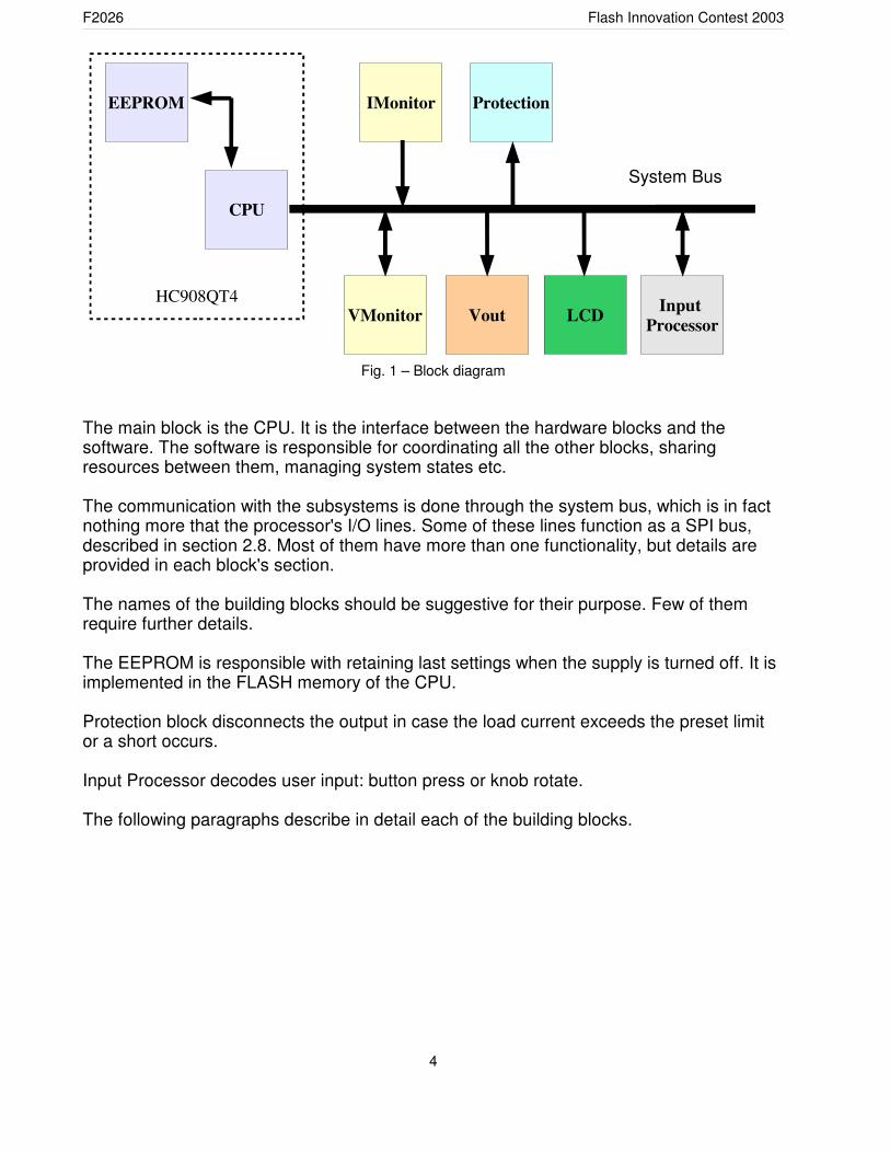
System Bus
Fig. 1 – Block diagram
The main block is the CPU. It is the interface between the hardware blocks and thesoftware. The software is responsible for coordinating all the other blocks, sharingresources between them, managing system states etc.
The communication with the subsystems is done through the system bus, which is in factnothing more that the processor's I/O lines. Some of these lines function as a SPI bus,described in section 2.8. Most of them have more than one functionality, but details areprovided in each block's section. The names of the building blocks should be suggestive for their purpose. Few of themrequire further details.
The EEPROM is responsible with retaining last settings when the supply is turned off. It isimplemented in the FLASH memory of the CPU.
Protection block disconnects the output in case the load current exceeds the preset limitor a short occurs.
Input Processor decodes user input: button press or knob rotate.
The following paragraphs describe in detail each of the building blocks.
4
HC908QT4
EEPROM IMonitor Protection
VMonitor Vout LCD Input Processor
CPU
F2026 Flash Innovation Contest 2003
2. Hardware
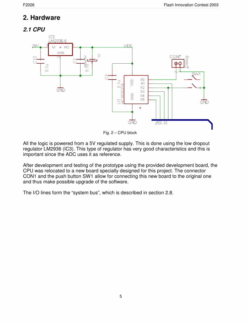
2.1 CPU
Fig. 2 – CPU block
All the logic is powered from a 5V regulated supply. This is done using the low dropoutregulator LM2936 (IC3). This type of regulator has very good characteristics and this isimportant since the ADC uses it as reference.
After development and testing of the prototype using the provided development board, theCPU was relocated to a new board specially designed for this project. The connectorCON1 and the push button SW1 allow for connecting this new board to the original oneand thus make possible upgrade of the software.
The I/O lines form the “system bus”, which is described in section 2.8.
5
F2026 Flash Innovation Contest 2003
2.2 IMonitor This block is responsible with monitoring the load current and informing the CPU aboutany faults.
Fig. 2 – IMonitor block
The current is sensed through R16 (0.1ohm/1%) placed on the “high side”. This meansthe measured current will also include the current drawn by LM338 (about 10mA).However, this will be subtracted in software. Moreover a precision of 10mA whenmeasuring the current is satisfactory for this application. The goal is to protect the loadand not to measure the current with a micro amp resolution.
The current drawn by the load is in range 0 – 2.5A. This will yield a voltage drop acrossR16 of approx. 0 – 250mV in the presence of a 28V common mode voltage. This signal ismeasured by the U2 (AD8200). From its datasheet:”AD8200 is a single-supply differenceamplifier for amplifying and low-pass filtering small differential voltages in the presence ofa large common-mode voltage.”Internally it has one amplifier with gain of 10 followed by a second amplifier with gain of 2.The connection between these 2 internal amplifiers is done through pins A1 and A2 (andone 100k resistor) allowing thus to externally implement a low pass filter (C11).
In this project the voltage drop across R16 is amplified 20 times and is send to the ADCthrough IC4A configured as a buffer. IC4A buffer is required because AD8200 is not able
6
F2026 Flash Innovation Contest 2003
to drive the line A5 (fan-in too high).
Iload = VR16/R16 – ILM338 = VR16 * 10 - ILM338
VA5 = (VR16 * 10) * 2 = 0 .. 5V
The final multiplication by 2 scales the input range of 0 – 2.5V to 0 – 5V, which isequivalent with improving ADC's resolution from approx. 19.5mV to 9.7mV. So, the currentis measured with a resolution of about 10mA.
The current through LM338 is almost constant. The software considers it as an offset andallows for calibration (set the value that will be subtracted from the output).
2.3 ProtectionThe role of this block is to disconnect the load in case of a short-circuit or a current biggerthan a preset value.
Fig. 3 – Protection block
It is build from a power MOSFET used as a controlled switch and a driver for it. IC2A is responsible with this task. According to superposition theorem:
VGS = (VOUT/2)*2 + (VCMD/2)*2 = VOUT + VCMD, where VCMD is either 0V or 5V.
7
F2026 Flash Innovation Contest 2003
The type of the power MOSFET is not critical. Any power MOSFET will work if it canwithstand at least 5V gate-source voltage.
Since it is a MOSFET transistor, its rDS resistance is in the range of few mili-ohms, so itdoes not need a heat sink.
This block is controlled directly by the pin A0 of the microcontroller. Immediately afterinitialization, A0 is set to “1” and the output is enabled. Every 5ms ImonitorTask (this block's mirror in software) checks the current through theload and, if this exceeds the preset limit, immediately sets A0 to “0” disconnecting thus theload. The system enters then into ALARM state from which only a RESET will allow exit.
This protection is doubled by the short-circuit protection inside LM338.
Remark:Apparently, the protection could be implemented more simple: just set the output voltageto 0V in case of a fault. Unfortunately it is very difficult to set the output voltage to exactly0V. Moreover this solution will have a longer response time.
2.4 VMonitor VMonitor continuously measures the output voltage.
Fig. 4 – VMonitor block
MCP42100 is a dual digital potentiometer of 100kohms, 8 bits resolution. This block usesonly half of it, designated as DP2. R18 and C8 form a reset circuit so that the
8
F2026 Flash Innovation Contest 2003
potentiometer always starts from a known initial state. The wiper voltage (between 0 and5V) is amplified 5 times by IC2B and then it is extracted from the output voltage by the U6(AD8200). The difference is amplified 10 times (5 * 2 because of R5) and low pass filtered(C10).
VA4 = (VOUT – VDP2 * 5) * 10
VOUT = VA4 / 10 + VDP2 * 5
For obtaining the best possible resolution, the difference in the above equation should bein the range 0 – 0.5V. The software controlling this block (VMonitorTask) continuously tries“to bring the difference in range” and then it takes a measurement.
Because the range 0 – 0.5V is scaled to 0 – 5V, the resolution of the measurements isapprox. 2mV over the entire output range 0 – 20V! This is equivalent with using a 14 bitADC!!! Actually this solution is better than using a 14 bit ADC because it is much less sensitive tonoise. In case of a 14 bit ADC, the ADC step is 305�V if the reference voltage is 5V.
9
F2026 Flash Innovation Contest 2003
2.5 VoutThis block is responsible with setting the output voltage.
Fig. 5 – Vout block
The power element is an integrated regulator LM338. It is mounted on a heat sink (seephotos), and in this schematic is only represented by the connector CON3. Also, therectifier bridge is mounted on a heat sink and is connected through the connector CON4. The transformer provides approx. 20VAC through CON2, which by rectifying gives about28V DC. C17 filters this voltage. R20 discharges C17 when the power supply is turned off.The 2 diodes 1N4004 protect the regulator LM338 from the C15, C16 discharge when thepower is turned off.
LM338 has a reference voltage of 1.24V typical, which normally means it is able to providean output voltage ranging from 1.2 to 32V. In order to obtain an output voltage startingwith 0V, its adjustment pin must be driven to 1.2V below the GND potential.
U3 (TC1121) is a charge pump voltage converter. It is powered at 5V and provides at the
10
F2026 Flash Innovation Contest 2003
output -5V. And it is a real trouble maker ! Its operating frequency of 200KHz is picked upby its neighbors. That is the reason for using C18, C19 and C20 besides the otherdecoupling capacitors. However, it provides the negative supply for IC1 (LM358).The positive supply for IC1 is obtained from 28V from which D1 subtracts approx. 5.6VThus IC1 “sees” approx. 28V between its power terminals (max. allowed is 32V).
MCP42100 (U4) is a dual digital potentiometer with 8 bits resolution. Its lower half, PA0-PB0-PW0 is designated as DP0. The second half, PA1-PB1-PW1, is designated as DP1.R15 is set so that DP0 “sees” 0.5V at input (this is equivalent to 2mV/step).
Thus, VADJ, the voltage at the output of IC1A is:
VADJ = VDP1 * 5 – VDP0 * 4
This output voltage has a resolution of approx. 8mV due to DP0.
The software operating this block is Vout module. It drives DP1 in steps of approx. 0.4Vand DP0 in steps of 2mV. Thus, the output voltage has no discontinuities over the entireoutput range 0 – 20V.
2.6 LCD The LCD display used is a 2 row 16 character module (SC1602BSLB) with backlight.
Fig. 6 – LCD block
In order to minimize the number of I/O pins, IC1 (74HC164) is used. It is a shift register of
11
F2026 Flash Innovation Contest 2003
8 bits. Also, the software never reads back data from LCD and that is why R/-W isconnected to GND. The disadvantage is that always, for any operation of the LCD, themaximum time specified in the datasheet is allocated.
The algorithm for sending some data to LCD is very simple: � load data into the shift register� set the appropriate value for RS line� enable LCD using E line and thus load data � disable E line
This way, only 3 I/O lines of the CPU are necessary to drive the LCD, and 2 of them canbe shared with other subsystems.
For the backlight R1 is used. The current required to illuminate the LCD is set to about60mA.
2.7 InputProcessorThis block is responsible with reading the user's input.
Fig. 7 – InputProcessor block
The low number of I/O pins imposes the usage of a multiplexing scheme. The powersupply has:� a RESET button used to escape the ALARM state, or to leave a menu � a SET button for settings� a rotary encoder for adjusting values and navigating menus
12

F2026 Flash Innovation Contest 2003
A2 pin of the CPU is used for reading the state of these buttons. 74HC164 register isshared with the LCD module. When the InputProcessorTask (the image in software of thisblock) runs, it sends appropriate codes to the shift register so that only one of IC2A, IC2B,IC2D is connected to A2 line. This way it is possible to read all the buttons.
2.8 System Bus
Fig. 8 – System bus
The CPU I/O lines represent the system bus. They software uses a multiplexing schemeso that each building block is allowed to access the bus without conflicting with others.
I/O line Function
A0 Command protection
A1 LCD E (enable) line
A2 InputProcessor – read buttons
A3 CS line on the SPI bus
A4 SCK line on the SPI bus and ADC inputfor voltage measurement
A5 SDA line on SPI bus and ADC input forcurrent measurement
Table 2 – System bus lines
13
IMonitor LCD
A0
A4
A1A2
A3
A5
Vout ProtectionVMonitor Input Processor

F2026 Flash Innovation Contest 2003
3. Software
3.1 OverviewThe brains of this project is the software. It is responsible with managing system states,managing resources and the interface with the user. In doing so, there is a softwarecorrespondent for each hardware block. Their interaction is managed by a simplepreemptive-cooperating operating system.
3.2 OSThis project is powered by a simple preemptive-cooperating operating system. It is a longname but the software behind it really does all the name says:� resource sharing� tasks management� priorities
In this project there are 5 tasks:� PowerSupplyTask� VMonitorTask� IMonitorTask� LCDTask� InputProcessor
IMonitorTask has the highest priority and it is allowed to interrupt any other task. Its job isto “continuously” check the current through load and, in case this exceeds a preset limit, todisable output and to signal an error condition. It is driven by the timer interrupt routine.
All the other tasks have the same priority. They are managed by a cooperative schedulerand this ensures there are no resource conflicts (I/O lines, global variables).
for(;;) { PowerSupplyTaskRun(); //run once through all tasks VMonitorTaskRun(); LCDTaskRun(); //update display 4 times/s InputProcessorRun();}
Though, IMonitorTask may interrupt each one of the other tasks and this could causeproblems. To avoid such situation, there are available 2 macros:
Cpu_DisableInt(); // disable all interruptsCpu_EnableInt(); // enable interrupts
Any critical section is delimited by these macros.
The files related to the operating system are:� Events.C – containing timer interrupt routine� nitro_power.C – containing initialization of the system and the scheduler
14
F2026 Flash Innovation Contest 2003
3.3 PowerSupplyTask This task represents the entire system at the software level. Its job is to transit the powersupply through different states according to the diagram below:
Fig. 9 – System states
K = knob event (UP or DOWN)E = error condition (current through load too high)S = set key pressedR = reset key pressed
On power on, the system is initialized by the main function and transits to RUNNING state.For any state except the ALARM, an error condition detected by the IMonitorTask willdetermine the system to transit to ALARM state ignoring the current operation. FromALARM state, only a R event will allow exit and will transit the system to RUNNING state.
For any MENU or submenu states, R will transit the system back to the RUNNING stateignoring the current operation. The settings are not updated in this case.
A knob event in RUNNING state will determine transition to MENU state. Further knobevents make possible to scroll through menu options. An S event will transit the system to
15
F2026 Flash Innovation Contest 2003
the selected submenu. In any submenu, knob events allow changing some setting's value.A second S event will update the value in the system's EEPROM and will return toRUNNING state.
PowerSupplyTask is implemented as a function, PowerSupplyTaskRun, that is calledonce for each passing through the for loop in scheduler. What it does is to check for anew message (from user or system) since only a message can trigger some action. Incase there is no such message/event, the function will return peacefully.
PowerSupplyTask makes use of the following variables:� userInputMessage – it is a buffer into which other subsystems put messages to be
processed� system_state – keeps the system state � vref – reference voltage used by the ADC (it is in fact the CPU power supply voltage).
Resolution is in mV.� stepA and stepB – see explanations below.� menu_option – helps in traversing the menu and selecting an option� step – see explanations below.� Ioff – the offset value to be subtracted from the computed Iout in order to cancel the
current drawn by LM338� Vout_reading – the measured output voltage, updated periodically by the
VMonitorTask.
Variables stepA and stepB require special treatment. In order to save memory andprocessing power, all the computations are done using integer arithmetic. However thiswill introduce some errors from rounding, integer division etc. In order to minimize theseerrors, the precision of the ADC quantization step used in computations must beincreased. An example will clarify this:
The ADC module has 8 bits resolution over the 0 to 5V input range. Without stepA andstepB and using integer arithmetic:
ADC step = 5V/256 = 19mV For a value of 200 returned by the ADC after measuring some signal it results:
Vsignal = 200*19 = 3.800V
Variables stepA and stepB are defined as:
stepA = (unsigned char)((vref * 10)/256);stepB = (unsigned char)((((vref * 10)%256)*10)/256);
This is equivalent with specifying the ADC step in 10microVolts increments/units! For thecase above this will yield:
stepA = 50V/256 = 195stepB = ((50V mod 256)*10)/256 = 3
16

F2026 Flash Innovation Contest 2003
Vsignal = (200*stepA)/10 + (200*stepB)/100 = (200*195)/10 + (200*3)/100 = 3.900 + 6 = 3.906V
The difference is significant ! And in case of some subsystems (VMonitor for instance) thisdifference would be even larger!!!
The step variable keeps a value (1 or 10) and is initialized by InputProcessor task. Somevalues (voltage, current etc.) need to be adjusted from time to time. In case of the voltage,resolution is 8mV. Changing the output voltage from 1V to 20V in steps of 8mV wouldrequire approx. 2375 knob UP events. A complete turn of the knob can trigger at most 24events!!! The user is not a probably a proficient high speed knob turner and surely this isnot his purpose.
Intuitively, when the desired output voltage is “far away” from the actual output voltage,any user will tend to rotate the knob faster. When getting close to target voltage, intuitivelythe user rotates the knob slower. Here is where step variable cames into play. TheInputProcessor task determines the knob speed and sets this variable to an appropriatevalue. If the speed is high, step will have a large value and that value is used by thePowerSuplyTask in doing settings. Thus, the above potential 100 knob turns are reducedto only 10. This is “automatically adjustable setting speed” from the feature list.
The files related to the PowerSupplyTask are:� PowerSupplyTask.c – � PowerSuplyTask.h – containing
3.4 VMonitorTaskVMonitorTask is the software module responsible with controlling VMonitor hardwareblock as described in section 2.4. It continuously tries to “bring the difference seen by theADC in range” by adjusting the DP2's output voltage. These adjustments are made insteps of approx.: (3 * 19mV) * 5 = 285mV. This is fast enough so that a trip over the entirerange takes 255 / 3 = 85 iterations, and it is fine enough so that always the differencebetween the output voltage and DP2 voltage can be “brought in range”.
The algorithm is very simple:
* enter critical section* get ADC lines* take measurement* exit critical section* if (in range)
* update Vout_reading# return
* else* try to bring in range by updating DP2 value # return
#
17
F2026 Flash Innovation Contest 2003
A few remarks concerning the code:� the variable Vout_reading is an int representing the output voltage in mV� in hardware, DP2 is connected the the SPI bus, and it is cascaded after DP1-DP0 (U4)
in order to save an I/O line.
VMonitorTask related files:� VmonitorTask.c� VmonitorTask.h
3.5 IMonitorTaskIMonitorTask works closely with IMonitor hardware block described in section 2.2. Thistask has the highest priority and runs once at every 5ms.
At every iteration, IMonitorTask measures the current through load and in case this ishigher than a preset limit (i_limit variable), disables the output and sends an ALARMmessage into the system.
The files related to this task are:� IMonitorTask.c� IMonitorTask.h
3.6 LCDTask This task is responsible with updating the display. In doing so it works closely with thePowerSuplyTask since the messages printed out depend on the system state.
Even if it is the largest software module in this project, its functioning is simple: � wait 250ms� update the display� start over
In counting time, lcd_counter variable is used. It is updated by the timer irq until it is 0.When this happens, LCDTask knows it has to refresh the display. It also reinitslcd_counter variable.
In order to minimize the ROM usage, the fragments of code called often were grouped intosmall functions. Examples are: ComputeI, LCDSendByte functions.
toChar function might need a little attention. It converts an unsigned decimal integer to astring using the following formula:
abcde = a*10000 + b*1000 + c*100 + d*10 + e= (((a*10 + b)*10 + c)*10 + d)*10 + e
18

F2026 Flash Innovation Contest 2003
This way, the algorithm becomes very simple and a huge reduction is obtained in ROMusage.
After the conversion ends, the first leading 0 is removed if present – 00.500V wouldn't betoo nice. And finally, the first 2 digits are shifted in order to insert the decimal point.
A nice trick is used to clear the display before updating it. The reason for doing so is thatusing the “real” command for clearing produces some unwanted effects:� the flickering is much more visible and annoying� sometimes the first character from a message gets “eated” - that could be only my
display, but being the only one available, I had to solve the problem somehow.
The idea is that any update will print out some message and this message will cover atleast the first half of the LCD row. So, it makes sense to clear only the second half. This isdone by printing space characters in the second half of the row. As positive side effects,the time used for erasing is minimized, and the flickering is reduced – most of the timeonly the last digit will change.
The files related to LCDTask are:� LCDTask.c� LCDTask.h
19
F2026 Flash Innovation Contest 2003
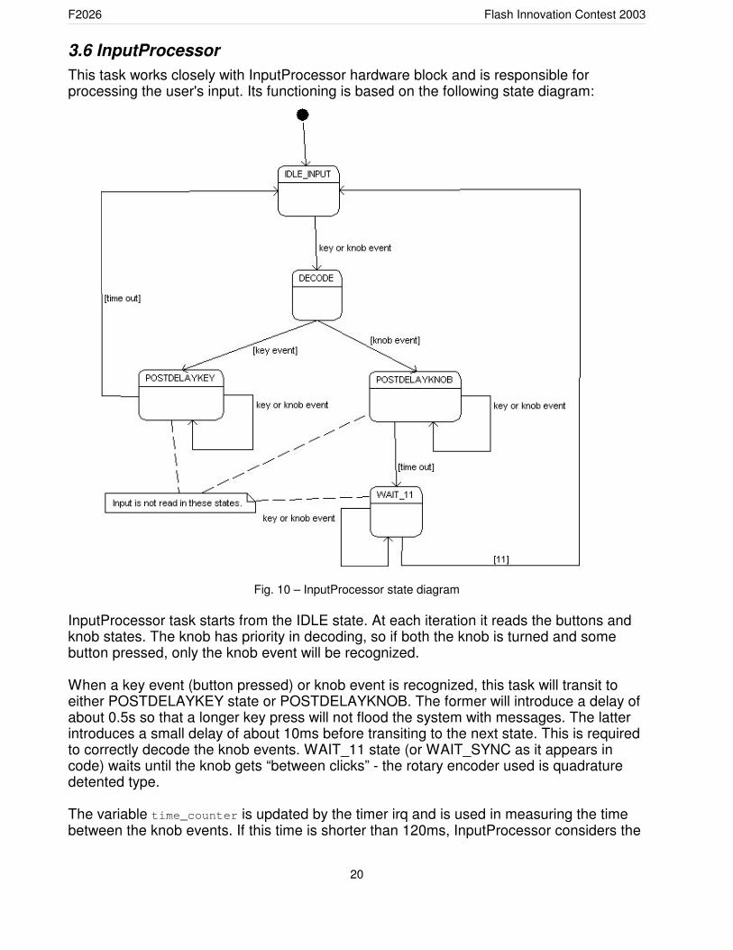
3.6 InputProcessorThis task works closely with InputProcessor hardware block and is responsible forprocessing the user's input. Its functioning is based on the following state diagram:
Fig. 10 – InputProcessor state diagram
InputProcessor task starts from the IDLE state. At each iteration it reads the buttons andknob states. The knob has priority in decoding, so if both the knob is turned and somebutton pressed, only the knob event will be recognized.
When a key event (button pressed) or knob event is recognized, this task will transit toeither POSTDELAYKEY state or POSTDELAYKNOB. The former will introduce a delay ofabout 0.5s so that a longer key press will not flood the system with messages. The latterintroduces a small delay of about 10ms before transiting to the next state. This is requiredto correctly decode the knob events. WAIT_11 state (or WAIT_SYNC as it appears incode) waits until the knob gets “between clicks” - the rotary encoder used is quadraturedetented type.
The variable time_counter is updated by the timer irq and is used in measuring the timebetween the knob events. If this time is shorter than 120ms, InputProcessor considers the
20

F2026 Flash Innovation Contest 2003
user is rotating the knob fast and consequently the variable step is set to value 10 (recall itis used by PowersupplyTask in adjustments). Otherwise, the step variable is initializedwith the value 1.
A remark: at each iteration, InputProcessor, before doing any input reading, checks the“system message queue”:
if (userInputMessage != I_ALARM) ...
The system message queue has a depth of only 1 message and if not carefully handledsome messages could be overwritten before being processed.
The files related to InputProcessor task are:� InputProcessor.c� InputProcessor.h
3.7 Vout moduleThis software module is in fact a group of functions called during the initialization of thesystem, and during functioning by the PowersupplyTask, when the output voltage ischanged. The hardware correspondent of this block is Vout module described in section 2.5.
Its functioning is based on the equation:
Vout = 1.24V + VADJ = 1.24V + VDP1 * 5 – VDP0 * 4
However, this is in theory because the op amps used will introduce some offset errors andalso the reference 1.24V could have a slightly different value. That is why a separatemeasurement block is required.
In adjusting the output voltage, DP0 is incremented/decremented in steps of 2mV, whileDP1 in steps of 0.4V. This way the output voltage will cover the range 0.6 – 20V withoutany discontinuities. The array v_steps keeps the values necessary to adjust DP1 in steps of 0.4V.
The files related to Vout module are:� Vout.c� Vout.h
21
F2026 Flash Innovation Contest 2003
3.8 SPI Bus2 of the CPU lines are used to communicate to some SPI peripherals (digitalpotentiometers) and this software module is responsible with controlling them.
It is implemented as a function that sends a byte over the bus. Also 2 macros weredefined: SPIBus_enable, SPIBus_disable.These macros are required because the lines A4 and A5 (clock and data) are shared withthe ADC.
The files related to SPI bus are:� SPIBus.c� SPIBus.h
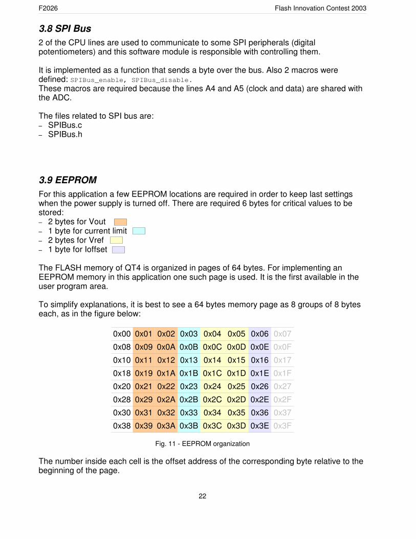
3.9 EEPROMFor this application a few EEPROM locations are required in order to keep last settingswhen the power supply is turned off. There are required 6 bytes for critical values to bestored:� 2 bytes for Vout � 1 byte for current limit � 2 bytes for Vref � 1 byte for Ioffset
The FLASH memory of QT4 is organized in pages of 64 bytes. For implementing anEEPROM memory in this application one such page is used. It is the first available in theuser program area.
To simplify explanations, it is best to see a 64 bytes memory page as 8 groups of 8 byteseach, as in the figure below:
0x00 0x01 0x02 0x03 0x04 0x05 0x06 0x07
0x08 0x09 0x0A 0x0B 0x0C 0x0D 0x0E 0x0F
0x10 0x11 0x12 0x13 0x14 0x15 0x16 0x17
0x18 0x19 0x1A 0x1B 0x1C 0x1D 0x1E 0x1F
0x20 0x21 0x22 0x23 0x24 0x25 0x26 0x27
0x28 0x29 0x2A 0x2B 0x2C 0x2D 0x2E 0x2F
0x30 0x31 0x32 0x33 0x34 0x35 0x36 0x37
0x38 0x39 0x3A 0x3B 0x3C 0x3D 0x3E 0x3F
Fig. 11 - EEPROM organization
The number inside each cell is the offset address of the corresponding byte relative to thebeginning of the page.
22

F2026 Flash Innovation Contest 2003
In the following paragraphs a small group of 8 bytes will be referred to as a block.
After erasure a memory page will be written block by block (8 times in this case) until it isfull. Then it will be erased again. Thus the endurance is increased from about 10000erase cycles to 80000.
A block has the following structure:
Offset inside block Meaning
0x00 Block written flag
0x01 Value of DP0
0x02 Value of DP1
0x03 Imax
0x04 Vref high byte
0x05 Vref low byte
0x06 Ioffset
0x07 reserved
The reason for defining a block as an 8 bytes group is to keep things as simple aspossible and to have a small reserve in case of a further development.
The requirements for the EEPROM subsystem in this application are very simple: retrievea previously saved value and update a value. In both cases it is required to locate the lastwritten block. For the former it will contain the value requested, for the latter it will help indeciding the next available block for writing into. It makes sense to have a routine to locatethe last written block and that is EEPROM_findLast.
The update function requires a way to write new values and from time to time a method toerase a memory page. These functionalities are provided by the 2 routines ERARNGEand PRGRNGE from the monitor.
#define ERARNGE 0x2806 // start address of the erase routine#define PRGRNGE 0x2809 // address of the program routine
These routines require a special buffer area in RAM from which they take the values to bewritten, address of the memory page, etc. The start address of this buffer is fixed. It isdeclared as a struct:
struct { unsigned char CTRLBYTE; // page erase or mass erase for ERARNGE unsigned char CPUSPD; // CPU clock in 0.25 MHz increments (approx) unsigned int LADDR; // last location to be written by PRGRNGE unsigned char DATA[8]; // EEPROM block has 8 bytes} EEBUFFER@0x0088; // put this at RAM+0x08 as requested by ROM routines
23
F2026 Flash Innovation Contest 2003
The update function is based on the following algorithm:
* find last written block * copy values to RAM buffer* put into RAM buffer the value to be updated* if there are no more empty blocks in the page
* erase page * determine next empty block * write RAM buffer into FLASH#
A few remarks about this function:� the VREF const was introduced and used in order to simplify updating of the Vref,
which is an int value.� PRGRNGE is a critical subroutine and is not recommended to interrupt it. It won't blow
the power supply but it will probably drive crazy any user attempting to change settings.That is why all the interrupts are disabled before calling it, and they are enabledafterward.
As a final remark, C makes possible an implementation very elegant and easy to follow. Itis also very easy to extend it with new functionalities. For instance a set of 3 EEPROMmemories could be implemented so that 3 different voltage/current settings could bestored and retrieved.
The files related to the EEPROM are:� EEPROM.c� EEPROM.h
4. OperationThis power supply was designed to be as user friendly as possible. The interface with theuser is very simple and comprises 2 push buttons, one knob (rotary encoder) and onedisplay.
The knob allows to scroll through the menus and to change some settings.SET button allows to select some menu or to update a setting's value into internalEEPROM.RESET button allows to exit any menu without updating any settings into EEPROM. If thevalue of a setting was changed before RESET was pressed, the change is lost afterRESET.Also RESET button allows to recover from ALARM state.
Before using the power supply for the first time, 2 calibrations must be made:� reference voltage� offset current
The “CalibrateVref” menu allows to calibrate the reference voltage. This is required
24
F2026 Flash Innovation Contest 2003
because the ADC uses as reference a voltage regulator, which is also used as a powersupply for the logic. The procedure is very simple and it must be done only once: � measure VDD� set new value – this can be set in the range 4.500V – 5.500V with a resolution of 1mV.The more exactly this value is specified, the more precise the measurements will be (Vout,Imax etc).
The second calibration refers to an offset current. This is introduced mainly by the LM338regulator since the current is measured on the high-side. The “Calibrate Ioff” menu allowsfor this calibration. The procedure is very simple:� select some resistor and set the output voltage so that the current through the resistor
is 100mA� adjust Ioffset until the displayed value is 0.100AThis procedure is required only once.
The other 2 menus (for setting Vout or Imax) are very simple to use .
5. References1 – HC908QT4 microcontroller datasheet (available from e-www.motorola.com)2 – LM338, LM2936-5 datasheets (available from www.national.com)3 – MCP42100 datasheet (available from www.microchip.com)4 – AD8200 datasheet (available from www.analog.com)5 – AN2346, AN1831 application notes from Motorola (e-www.motorola.com)
25


![Project Report[1].Doc](https://static.fdocuments.in/doc/165x107/55cf9df4550346d033b0063f/project-report1doc.jpg)


![[ Project ].doc](https://static.fdocuments.in/doc/165x107/54ced9c44a79590d788b45d5/-project-doc.jpg)