project
22
Study of FPGA using VHDL in partial fulfillment of the requirements of the Global Internship Program in Engineering Design and Innovation GIPEDI under the aegis of Foundation for Innovation and Technology Transfer Indian Institute of Technology Delhi Akanksha Singh 03202072013 Mtech VLSI Indira Gandhi Delhi Technical University for Women Kashmere Gate, Delhi 110006 INDIA Research Supervisor : Prof. Subrat Kar Student Mentor : Ms. Harika Aennam Indian Institute of Technology Delhi Hauz Khas,New Delhi 110016 INDIA
-
Upload
paras-kapoor -
Category
Documents
-
view
105 -
download
2
Transcript of project

Study of FPGA using VHDL
in partial fulfillment of the requirements ofthe Global Internship Program in Engineering Design and Innovation
GIPEDIunder the aegis of Foundation for Innovation and Technology Transfer
Indian Institute of Technology Delhi
Akanksha Singh03202072013Mtech VLSI
Indira Gandhi Delhi Technical University for WomenKashmere Gate, Delhi 110006 INDIA
Research Supervisor : Prof. Subrat Kar
Student Mentor : Ms. Harika Aennam
Indian Institute of Technology DelhiHauz Khas,New Delhi 110016 INDIA
Acknowledgement
This report is submitted by Akanksha Singh and Paras Kapoor in the fulfillment ofthe study of FPGA. It is with deep sense of gratitude and reverence that we express oursincere thanks to our guide Prof. Subrat Kar for his guidance, encouragement, help anduseful suggestions throughout their untiring and painstaking efforts, methodical approachand individual help made it possible for us to complete this work in time. His guidance andscientific approach served a valuable incentive for completion of this work.We would liketo express our sincere gratitude to our head student mentor Ms. Harika Aennam andMr. Shailesh Singh for their continued support and encouragement throughout thecourse of this work. Their valuable expertise and advice made this work possible. We shallever remain indebted to members of Photonics lab of Indian Institute of Technology, Delhifor their co-operation kindness and general help extended to us during the completion ofthis work.
Contents
1 Introduction I1.1 Motivation . . . . . . . . . . . . . . . . . . . . . . . . . . . . . . . . . . . I1.2 Literature Survey . . . . . . . . . . . . . . . . . . . . . . . . . . . . . . . I1.3 ORGANISATION OF REPORT . . . . . . . . . . . . . . . . . . . . . . . III
2 Methodology, Approach and Tools III2.1 Tools We Used . . . . . . . . . . . . . . . . . . . . . . . . . . . . . . . . III2.2 Work Done . . . . . . . . . . . . . . . . . . . . . . . . . . . . . . . . . . III
2.2.1 EXPERIMENT-1 . . . . . . . . . . . . . . . . . . . . . . . . . . . III2.2.2 EXPERIMENT-2 . . . . . . . . . . . . . . . . . . . . . . . . . . . V2.2.3 EXPERIMENT-3 . . . . . . . . . . . . . . . . . . . . . . . . . . . VII2.2.4 EXPERIMENT-4 . . . . . . . . . . . . . . . . . . . . . . . . . . . IX2.2.5 EXPERIMENT-5 . . . . . . . . . . . . . . . . . . . . . . . . . . . XI2.2.6 EXPERIMENT-6 . . . . . . . . . . . . . . . . . . . . . . . . . . . XIII
3 Result and Conclusions XIV3.1 Summary of work . . . . . . . . . . . . . . . . . . . . . . . . . . . . . . . XIV3.2 Significance of these Experiments . Interpretation of these Experiments: . XIV3.3 Explaination of intuitive results: . . . . . . . . . . . . . . . . . . . . . . . XIV3.4 Explaination of usual results . . . . . . . . . . . . . . . . . . . . . . . . . XV
4 Future Work XV4.1 What could I have done . . . . . . . . . . . . . . . . . . . . . . . . . . . XV4.2 What more can the next person do . . . . . . . . . . . . . . . . . . . . . XVI
List of Figures
1 RTL generated . . . . . . . . . . . . . . . . . . . . . . . . . . . . . . . . IV2 RTL generated . . . . . . . . . . . . . . . . . . . . . . . . . . . . . . . . V3 This figure shows results of DCM-Clock Multiplication and Division. . . VI4 RTL generated . . . . . . . . . . . . . . . . . . . . . . . . . . . . . . . . VII5 This figure shows results of PRBS by keeping taps at positions 9,7,6,5,3,1 VIII6 RTL generated . . . . . . . . . . . . . . . . . . . . . . . . . . . . . . . . IX7 This figure shows results of Encoding and Decoding PRBS. . . . . . . . . X8 This figure shows results of FSM(output using UART). . . . . . . . . . . XI9 This figure shows results of FSM(output using UART). . . . . . . . . . . XII10 This figure shows results of Encoding and Decoding PRBS. . . . . . . . . XIII
List of Tables
1 Introduction
1.1 Motivation
Short for Field-Programmable Gate Array, a type of logic chip that can be programmed.An FPGA is similar to a PLD, but whereas PLDs are generally limited to hundreds ofgates, FPGAs support thousands of gates. They are especially popular for prototypingintegrated circuit designs. Once the design is set, hardwired chips are produced for fasterperformance.Programming FPGA is done with VHDL. VHDL is VHSIC Hardware Discription Lan-guage.Major motivation was from the study of embedded system course. Prototyping ICs.Programming FPGA, checking the design using simulations and then generating RTL.
1.2 Literature Survey
This document summarizes the findings of an in-depth study into the Field programmableGate Arrays (FPGAs). An extensive study of FPGA has been done by performing variedtasks/experiments related to the field. The FPGA board studied was SPARTAN 3E andATLYS family SPARTAN. The module of DCMhas been described in [1]. Digital ClockManagers (DCMs) provide advanced clocking capabilities to SpartanTM-3 FPGA appli-cations. DCMs optionally multiply or divide the incoming clock frequency to synthesizea new clock frequency. DCMs also eliminate clock skew, thereby improving system per-formance.Sandeep Mukherjee, Ruchir Pandey in [2] describes the Pseudo random binary sequence,which is essentially a random sequence of binary numbers. So PRBS generator is noth-ing but random binary number generator. It is ‘random’ in a sense that the value ofan element of the sequence is independent of the values of any of the other elements.Asequence of consecutive n ∗ (2n − 1) bits comprise one data pattern, and this pattern willrepeat itself over time.
Rod Jesman,Fernando Martinez Vallina,Jafar Saniie in [3] explains the complete hardwareand software processor system design . The MicroBlaze is a virtual microprocessor thatis built by combining blocks of code called cores inside a Xilinx Field ProgrammableGate Array (FPGA). The MicroBlaze processor is a 32-bit Harvard Reduced InstructionSet Computer (RISC) architecture optimized for implementation in Xilinx FPGAs withseparate 32-bit instruction and data buses running at full speed to execute programs andaccess data from both on-chip and external memory at the same time.This flexibilityallows the user to balance the required performance of the target application against thelogic area cost of the soft processor.
I

References :[1] XAPP462 (V1.1) January 5 , 2006 XILINX “Using Digital Clock Managers (DCMs)in Spartan-3 FPGAs” .[2] Sandeep Mukherjee, Ruchir Pandey “design and implementation of prbs generator us-ing vhdl” Department of Electronics and Communication Engineering National Instituteof Technology ,Rourkela ,2007[3] Rod Jesman,Fernando Martinez Vallina,Jafar Saniie “MicroBlaze Tutorial Creating aSimple Embedded System and Adding Custom Peripherals Using Xilinx EDK SoftwareTools”, Embedded Computing and Signal Processing Laboratory – Illinois Institute oftechnology,2006
II
1.3 ORGANISATION OF REPORT
1. Section 1 : contains the acknowledgement, motivation and the literature survey.
2. Section 2 : This section of the report explains the methology,approach and toolsused to perform the various tasks. The objective of the experiments along with thedetailed theory and simulation results also have been included.
3. Section 3 : comprises of the result of the tasks and the conclusions drawn fromthe tasks along with the intuitive results.
4. Section 3 : During the learning phase of FPGA several challeges were faced whichwill be dealt with the course of time, henceforth this section contains the desiredfuture work to be accomplished.
2 Methodology, Approach and Tools
2.1 Tools We Used
Xilinx ISEWebpack 12.1FPGA BOARD : SPARTAN 3EDEVICE :XC3S500EPACKAGE :FG320SYNTHESIS TOOL : XST(VHDL)SIMULATOR : ISiM
2.2 Work Done
2.2.1 EXPERIMENT-1
Objective: To implement basic logic gates on FPGA Spartan3E.Approach : Digital systems are said to be constructed by using logic gates. These gatesare the AND, OR, NOT, NAND, NOR, XOR and XNOR gates.
III

Figure 1: RTL generated
RESULT : The basic logic gates have been implemented on FPGA Spartan 3E.
IV
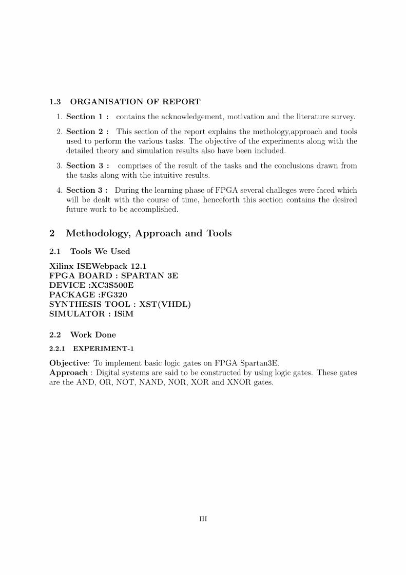
2.2.2 EXPERIMENT-2
Objective: Clock division , multiplication and phase shift using the DCM module.
Approach : The Digital Clock Manager (DCM) primitive in Xilinx FPGA parts isused to implement delay locked loop, digital frequency synthesizer, digital phase shifter,or a digital spread spectrum. The digital clock manager module is a wrapper aroundthe DCM primitive which allows it to be used in the EDK tool suite. Digital ClockManagers (DCMs) provide advanced clocking capabilities to Spartan-3 Generation FPGAapplications (Spartan-3, Spartan-3E, Spartan-3A, Spartan-3AN, and Spartan-3A DSPfamilies). Primarily, DCMs eliminate clock skew, thereby improving system performance.Similarly, a DCM optionally phase shifts the clock output to delay the incoming clock bya fraction of the clock period. DCMs optionally multiply or divide the incoming clockfrequency to synthesize a new clock frequency. The DCMs integrate directly with theFPGA’s global low-skew clock distribution network.
Figure 2: RTL generated
V

OUTPUT:
Figure 3: This figure shows results of DCM-Clock Multiplication and Division.
RESULT : Using the DCM module a clock of 100 MHz was divided by a factor of 3 andmultiplied by a factor of 4.
VI

2.2.3 EXPERIMENT-3
Objective: Make a 9 digit PRBS and test the repeat cycle using a osciloscope.
Approach: Pseudo random binary sequence is essentially a random sequence of binarynumbers.So PRBS generator is nothing but random binary number generator. It is random in asense that the value of an element of the sequence is independent of the values of any ofthe other elements. It is pseudo because it is deterministic and after N elements it startsto repeat itself, unlike real random sequences.
Figure 4: RTL generated
VII

OUTPUT:
Figure 5: This figure shows results of PRBS by keeping taps at positions 9,7,6,5,3,1
RESULT: 9 digit PRBS has been simulated and implemented.
VIII

2.2.4 EXPERIMENT-4
Objective: Make a FSM to do the following:Each bit of the PRBS is to be encoded using a Gray code , transmitted and Gray Codeencoder and decoder (both to be implemented on the same FPGA).There should be one input to control whether it should work as a encoder or decoder.Input is from encoder is parallel.Input to decoder is parallel.CLK is common.
Approach:
1. The random binary sequence is generated using PRBS.
2. This generated random sequence is now fed to the 9 bit encoder which will convertit to gray sequence.
3. Input is from encoder is parallel.
4. Input to decoder is parallel
5. The generated gray sequence is converted back to binary sequence using a 9 bitdecoder.
Figure 6: RTL generated
IX
OUTPUT:
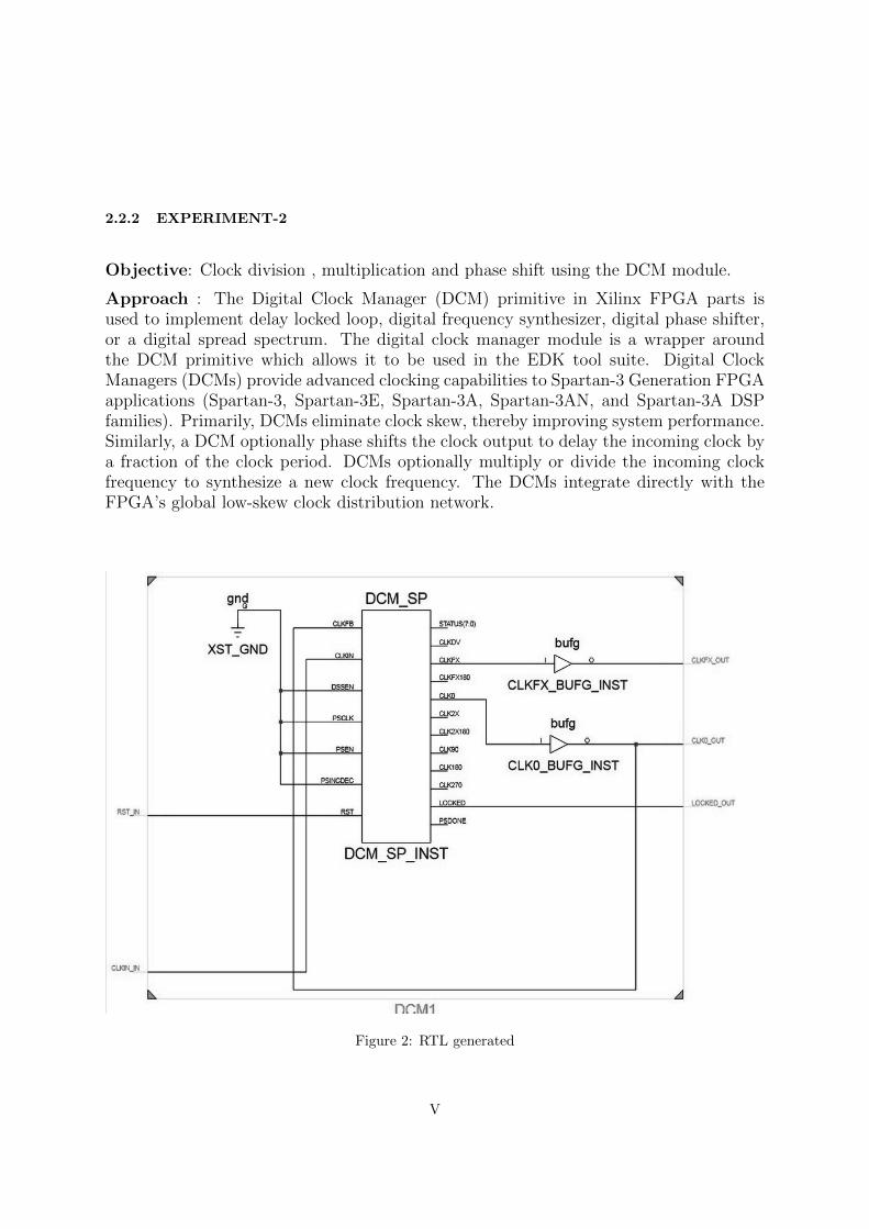
Figure 7: This figure shows results of Encoding and Decoding PRBS.
X

2.2.5 EXPERIMENT-5
Objective: Repeat Expt 3 with the following difference:1.Output from encoder is serial.2.Input to decoder is serial.3.Show both encoder o/p and decoded output on a oscilloscope.
Approach: The Universal Asynchronous Receiver/Transmitter (UART) controller is thekey component of the serial communications subsystem of a computer. The UART takesbytes of data and transmits the individual bits in a sequential fashion. At the destina-tion, a second UART re-assembles the bits into complete bytes. Serial transmission iscommonly used with modems and for non-networked communication between computers,terminals and other devices.
Figure 8: This figure shows results of FSM(output using UART).
XI

OUTPUT:
Figure 9: This figure shows results of FSM(output using UART).
XII
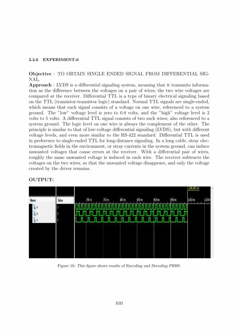
2.2.6 EXPERIMENT-6
Objective : TO OBTAIN SINGLE ENDED SIGNAL FROM DIFFERENTIAL SIG-NAL.Approach : LVDS is a differential signaling system, meaning that it transmits informa-tion as the difference between the voltages on a pair of wires; the two wire voltages arecompared at the receiver. Differential TTL is a type of binary electrical signaling basedon the TTL (transistor-transistor logic) standard. Normal TTL signals are single-ended,which means that each signal consists of a voltage on one wire, referenced to a systemground. The ”low” voltage level is zero to 0.8 volts, and the ”high” voltage level is 2volts to 5 volts. A differential TTL signal consists of two such wires, also referenced to asystem ground. The logic level on one wire is always the complement of the other. Theprinciple is similar to that of low-voltage differential signaling (LVDS), but with differentvoltage levels, and even more similar to the RS-422 standard. Differential TTL is usedin preference to single-ended TTL for long-distance signaling. In a long cable, stray elec-tromagnetic fields in the environment, or stray currents in the system ground, can induceunwanted voltages that cause errors at the receiver. With a differential pair of wires,roughly the same unwanted voltage is induced in each wire. The receiver subtracts thevoltages on the two wires, so that the unwanted voltage disappears, and only the voltagecreated by the driver remains.
OUTPUT:
Figure 10: This figure shows results of Encoding and Decoding PRBS.
XIII

3 Result and Conclusions
3.1 Summary of work
Experiments Performed by us:
• Make simple AND / OR / NOR / XNOR gates and test them with a multimeter
• Use DCM clocking wizard and Multiply and Divide Clock input.
• Make a linear feedback shift register based PRBS with 7 registers and test therepeat cycle using a oscilloscope. You will need to generate a timing pulse for theoscilloscope in order to do this.
• Each bit of the PRBS is to be encoded using a Gray code , transmitted and GrayCode encoder and decoder (both to be implemented on the same FPGA). Thereshould be one input to control whether it should work as a encoder or decoder.
• O/p from encoder is serial. I/p to decoder is serial.
• Low Voltage Differential Signals were Converted to single ended TTL signals. Showboth encoder o/p and decoded o/p on a oscilloscope.
3.2 Significance of these Experiments . Interpretation of these Experiments:
• We learnt the basics of FPGA programming through VHDL.
• In Exp.2 we understood how the DCM modules of an FPGA can be used to providedifferent type of clock input itself in FPGA.
• In Exp.3 we understood the implementation of PRBS though VHDL structural levelprogramming.
• In Exp.4 we understood how FPGA communicates serially through a PC using aUART cable and a fixed baud rate.
• In Exp.5 we learnt how CPU can be implemented on an FPGA using fetch, decodeand execute operation though VHDL entities.
• In Exp.6 we learnt how LVDS signals are converted to TTL signals.
3.3 Explaination of intuitive results:
• Experiment 1 is about the implementation of different logic gates on FPGA. Theinput was given using GPIO switches and the output was seen using LEDs.
• Experiment 2 is about the usage of DCM modules of an FPGA. The default Clockfrequency was scaled using DCM modules. The RESET is set HIGH for some clockcycles to remove the locked outputs.
XIV

• Experiment 3 is about Random Sequence Generation. The VHDL entity generatesa 9 bit random number and repeats the cycle after 2n − 1.
• Experiment 4 is about Encoding the PRBS output to grey code using a Encoderand again decoding back to binary using a Decoder.
• Experiment 5 is about serially transmitting between encoder and decoder. DifferentClocks were given to the components. The input clock to the encoder and decoderwas 9 times the input clock to PRBS. A delayed output from encoder was taken toremove errors.
• Experiment 6 is about how LVDS signals are converted to TTL signals using ibufdscomponent instantiation.
3.4 Explaination of usual results
• In Experiment 1 Simple Logic Gates were implemented.
• In Experiment 2 An input clock of 100 MHz was multiplied to 400 Mhz and dividedto 33.33 Mhz using single DCM module.
• In Experiment 3 A Random 9 bit sequence was generated using D Flip Flop. TheMax length sequence was implemented using few bits of output as caps and Xoringtheir output to first bit.
• In Experiment 4 the encoded version of the PRBS was generated as a grey code anddecoded back again to binary. Grey to Binary mechanism was used in decoder andvice versa.
• In Experiment 5 the output from Encoded is transmited serially to Decoder. Dif-ferent Clocks were given to the components. The input clock to the encoder anddecoder was 9 times the input clock to PRBS. A delayed output from encoder wastaken to remove errors.
• In Experiment 6 Two Differential digital signals were converted to A single endedTTL signal using ibufds component instantiation.
4 Future Work
4.1 What could I have done
Use a 8-bit CPU on a Spartan 3E kit to achieve PRBS generation, Encoder, Decoder andSerially outputing through UART cable .Use a UART with a fixed baud rate.Use a 8-bit / 32-bit soft CPU (picoblaze/microblaze) to multiply two 3x3 matrices to-gether.Each element of the matrices is a 8 bit number.
XV

4.2 What more can the next person do
• Implement those experiments to other FPGA boards.
• Make 16 bit CPU using Power PC.
• Use the PRBS generation for Optical Communication.
XVI

Akanksha Singh I year Postgraduate student
Department of Electronics Engineering
Indira Gandhi Delhi Technical University for Women, Delhi Email: [email protected]
New Delhi -110006 ph: +91-9540297264
EDUCATION Indira Gandhi Delhi Technical University for Women, Delhi July’13 onwards
M-Tech in VLSI Design, Percentage: 79%
National Institute of Technology, Raipur May’13
B-Tech in Electronics & T.Comm. CGPA: 7.62/10
St. Clare’s Sr. Sec. School, Agra May 2008
Class XII (AISSE) – CBSE Percentage: 89.8%
St. Clare’s Sr. Sec. School, Agra May 2006
Class X (AISSCE) – CBSE Percentage : 92.8%
COURSES
COURSES Departmental courses: Cmos Analog Circuits, Digital Integrated Circuits, Hardware Description
DONE DONE Language, Semiconductor device, Advanced IC processing, Deep Submicron CMOS IC’s,CMOS
mixed-signal VLSI design, IC for Analog Signal Processing, VLSI Subsystem design, Device M-
odelling & circuit simulation ,Analog circuits, Digital Electronics, Control Systems, Signals &
systems, EMT, Communication systems, Network Theory, Industrial Instrumentation, Advan-
ced Microprocessor & interfacing, Digital signal processing, Electrical Machines
Relevant non-departmental courses: Intro. To Computers And Programming, Basic Principles
Of Elect. Engg , programming in C and C++, environmental education, Basic mechanical,
Egineering drawings, Engineering mathematics
TECHNICAL Programming: VHDL, Verilog, Pspice, Latex, C/C++, Linux, MATLAB
SKILLS Engineering tools : ORCAD Pspice 16.6 , Xilinx ISE 13.2, Tanner EDA, Keil MicroVision-2,
LINUX RHEL-6, Cisco packet tracer 5.3, MULTISIM, Microsoft Excel
ACADEMIC DTMOS transistor with source follower Sub circuit Jan’14-present
PROJECTS PROJECTS Environment: Analog ,0.18um technology, ORCAD Pspice 16.6
A novel technique to achieve high gain bandwidth product at low voltage
Simulation using Pspice to calculate the bandwidth and verification by manual calculations
Face recognition using Eigen faces Aug’13-Nov’13
Environment: Digital signal processing, MATLAB
This approach considers training, where the face database is created and the projection matrix, the
one that achieve the dimensional reduction, is obtained from all the database face images.
Mean face is calculated and reduced representation of each database image with respect it.
Water Level Controller Using Microcontroller AT89S52 Jan’13-Mar’13
Environment: Embedded System , Keil MicroVision-2 , soldering performed
Use conductive sensor to control the working of pump. The Copper probes are used to sense the
water level. The probes are inserted into the water tank whose level of water is to be monitored.
This water-level Controller-cum-alarm circuit is configured around the well-known 8 bit
Microcontroller 8085. It also switches off the solenoid valve when the tank is full and
automatically switches it on when the water level is low. The hardware is assembled using various
components and fabricated using mechanical and electrical fabrication.
Corporate network with advanced routing, switching and security May’12-June’12
Environment: Networking , Cisco packet tracer
Carried out the design of a two office’s network infrastructure using 5 ISP Routers.
Applied advanced switching for vlans and STP , VTP and switch port security, Intervlan routing
and Applied access list control

AWARDS & AIEEE: All India Rank 12021 out of 12 lakh students appeared for AIEEE 2009
HONOURS PAPER PRESENTATION: Awarded 3rd
prize for state level PRASTUTI, 2011
CERTIFICATE: district level for securing above 90%in mother language HINDI
AISSCE: Awarded certificate for securing highest marks in English in 10th board exam
Certificate of merit: for academics in school for the year 2007-2008
NSTSE: All India Rank 836 in NSTSE -2008
INTERNSHIP Hewlett Packard Education Services, Noida May’12-June’12
Training on network management and security.
Carried out work on Cisco packet tracer 5.3
Configuring static routes, packet filtering and network address translation using Red hat Linux
Studied about advanced routing
All India Radio, Agra May’11-June’12
Studied the various sections of ALL INDIA RADIO broadcasting and appropriate execution
and working of the news studios and capacitive Earth Station.
Studied the acoustic treatment provided in studios , control rooms, and other technical areas
The various digital modulation techniques available for radio signal transmission
INTERPER- 1. President of West Girls Hostel, IGDTUW July’13 onwards
SONAL 2. President of Hostel-G , NIT Raipur July’12-13
SKILLS 3. Hostel Mess Committee member June’11-13
4. Coordinator –Marketing , Eclectika June’11-12
5. Literary committee member July’09-10
6. Event Coordinator Mar’11
7. House Captain June’06-08
8. Won 2nd
prize for skit competition, ASSET Oct’11
9. Anchoring in various college and state level events
10. Won District level Drawing Competition Feb’08
11. Active participant in sports and have won many award at school and district level
12. District level Basketball player
13. Awarded prize for intra-school Group Singing Sep’05
OTHER meeting people of diverse culture, music, painting and decoration
INTERESTS


![[INSERT PROJECT NAME]€¦ · Project name Project Number [Where applicable] Project Manager Project Controller Project location [Insert brief details of project location, including](https://static.fdocuments.in/doc/165x107/603496f741d854077e52cec0/insert-project-name-project-name-project-number-where-applicable-project-manager.jpg)