Progress in the LumiCal readout electronics · Progress in the LumiCal readout electronics ......
17
Progress in the LumiCal readout electronics Marek Idzik AGH-UST Faculty of Physics and Applied Computer Science AGH University of Science and Technology 25th FCAL Collaboration Workshop VINCA Belgrade 12-13 October 2014
Transcript of Progress in the LumiCal readout electronics · Progress in the LumiCal readout electronics ......
Progress in the LumiCal readout electronics
Marek Idzik AGH-UST
Faculty of Physics and Applied Computer ScienceAGH University of Science and Technology
25th FCAL Collaboration Workshop VINCA Belgrade 12-13 October 2014
Outline
• Introduction and Where we are• ASIC developments in CMOS 130 nm– Analog front-end– ADC conversion
• Summary and Plans
3
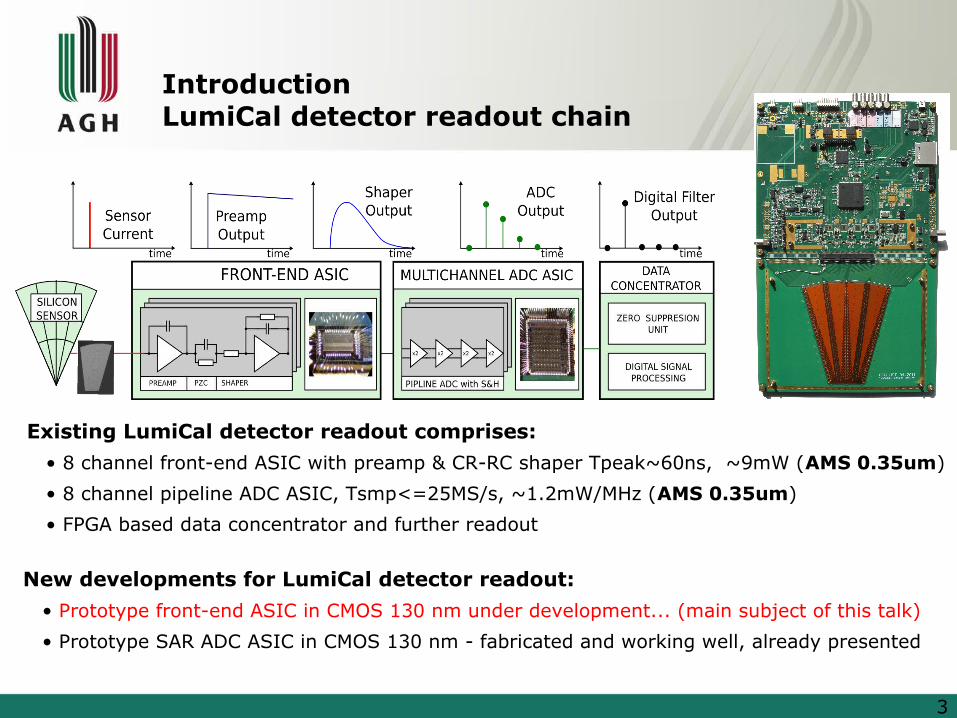
IntroductionLumiCal detector readout chain
Existing LumiCal detector readout comprises:
• 8 channel front-end ASIC with preamp & CR-RC shaper Tpeak~60ns, ~9mW (AMS 0.35um)
• 8 channel pipeline ADC ASIC, Tsmp<=25MS/s, ~1.2mW/MHz (AMS 0.35um)
• FPGA based data concentrator and further readout
New developments for LumiCal detector readout:
• Prototype front-end ASIC in CMOS 130 nm under development... (main subject of this talk)
• Prototype SAR ADC ASIC in CMOS 130 nm - fabricated and working well, already presented
4
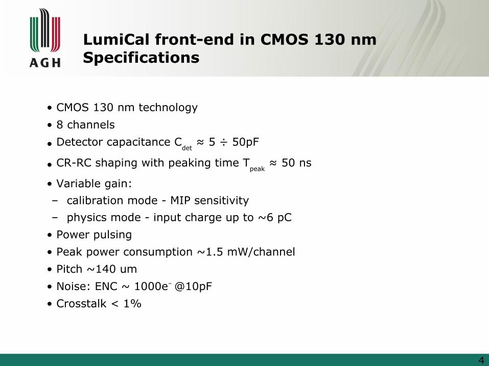
LumiCal front-end in CMOS 130 nmSpecifications
• CMOS 130 nm technology
• 8 channels
• Detector capacitance Cdet
≈ 5 ÷ 50pF
• CR-RC shaping with peaking time Tpeak
≈ 50 ns
• Variable gain:
– calibration mode - MIP sensitivity
– physics mode - input charge up to ~6 pC
• Power pulsing
• Peak power consumption ~1.5 mW/channel
• Pitch ~140 um
• Noise: ENC ~ 1000e– @10pF
• Crosstalk < 1%
5
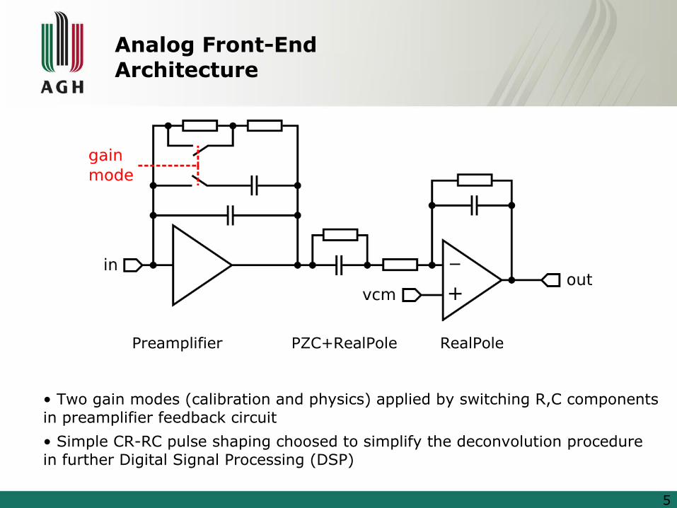
Analog Front-EndArchitecture
Preamplifier PZC+RealPole RealPole
• Two gain modes (calibration and physics) applied by switching R,C components in preamplifier feedback circuit
• Simple CR-RC pulse shaping choosed to simplify the deconvolution procedure in further Digital Signal Processing (DSP)
6
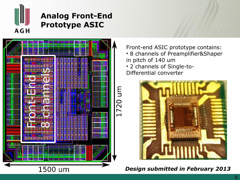
Analog Front-EndPrototype ASIC
Design submitted in February 2013
Front-end ASIC prototype contains:• 8 channels of Preamplifier&Shaper in pitch of 140 um• 2 channels of Single-to-Differential converter
7
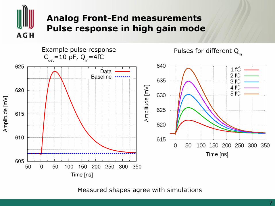
Analog Front-End measurementsPulse response in high gain mode
Example pulse response C
det=10 pF, Q
in=4fC
Pulses for different Qin
Measured shapes agree with simulations
8
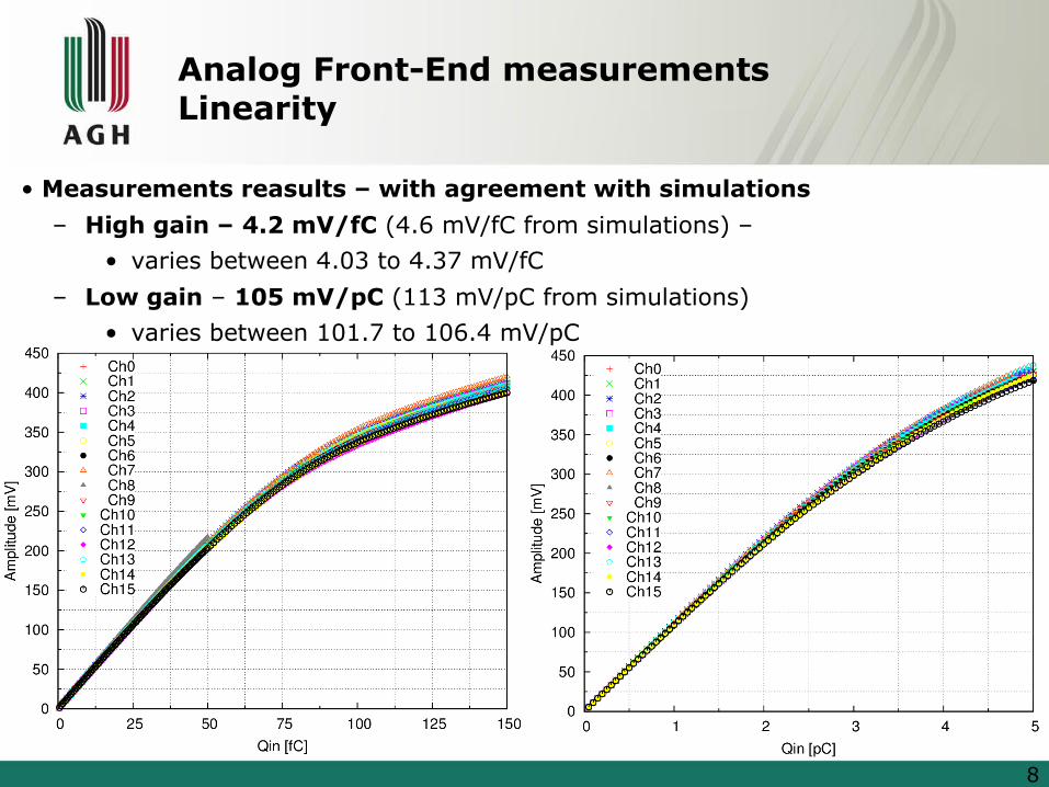
Analog Front-End measurementsLinearity
• Measurements reasults – with agreement with simulations
– High gain – 4.2 mV/fC (4.6 mV/fC from simulations) –
• varies between 4.03 to 4.37 mV/fC
– Low gain – 105 mV/pC (113 mV/pC from simulations)
• varies between 101.7 to 106.4 mV/pC
9
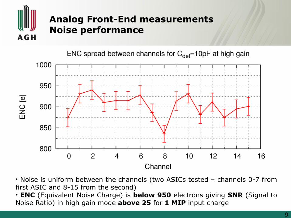
Analog Front-End measurementsNoise performance
• Noise is uniform between the channels (two ASICs tested – channels 0-7 from first ASIC and 8-15 from the second)• ENC (Equivalent Noise Charge) is below 950 electrons giving SNR (Signal to Noise Ratio) in high gain mode above 25 for 1 MIP input charge
10
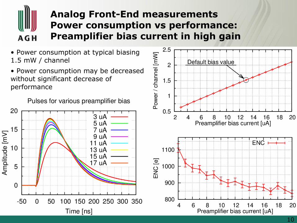
Analog Front-End measurementsPower consumption vs performance:Preamplifier bias current in high gain
• Power consumption at typical biasing 1.5 mW / channel
• Power consumption may be decreased without significant decrease of performance
11
Analog Front-End measurementsSummary
• Measurements results agree with simulations and specifications– Pulse shape and peaking time (50ns) as excepted– Gains in both modes differs within 10% from simulated– Baseline spread below 25 mV– Noise ENC at 10 pF below 1000 e-– Crosstalk measuremets:
• High gain – 0.64%• Low gain – 0.80%
– Power consumtion ~1.5 mW/channel – can be reduced by lowering bias currents
– All parameters uniform between channels (two ASICs measured)
• Detector capacitance measurements needs to be finished...
12
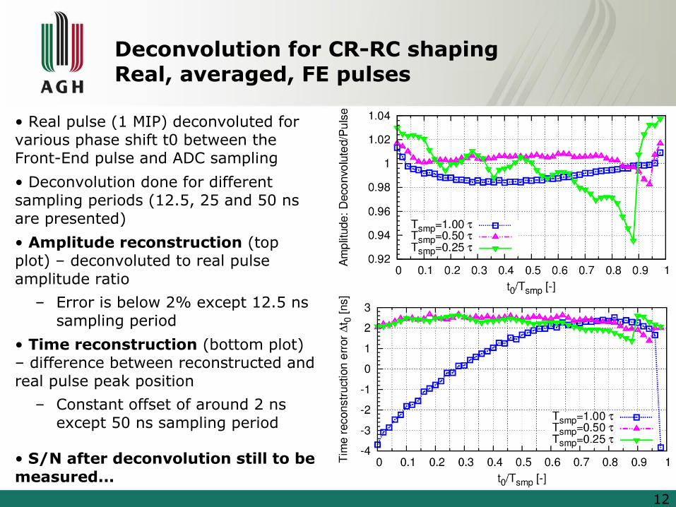
Deconvolution for CR-RC shapingReal, averaged, FE pulses
• Real pulse (1 MIP) deconvoluted for various phase shift t0 between the Front-End pulse and ADC sampling
• Deconvolution done for different sampling periods (12.5, 25 and 50 ns are presented)
• Amplitude reconstruction (top plot) – deconvoluted to real pulse amplitude ratio
– Error is below 2% except 12.5 ns sampling period
• Time reconstruction (bottom plot) – difference between reconstructed and real pulse peak position
– Constant offset of around 2 ns except 50 ns sampling period
• S/N after deconvolution still to be measured...
13
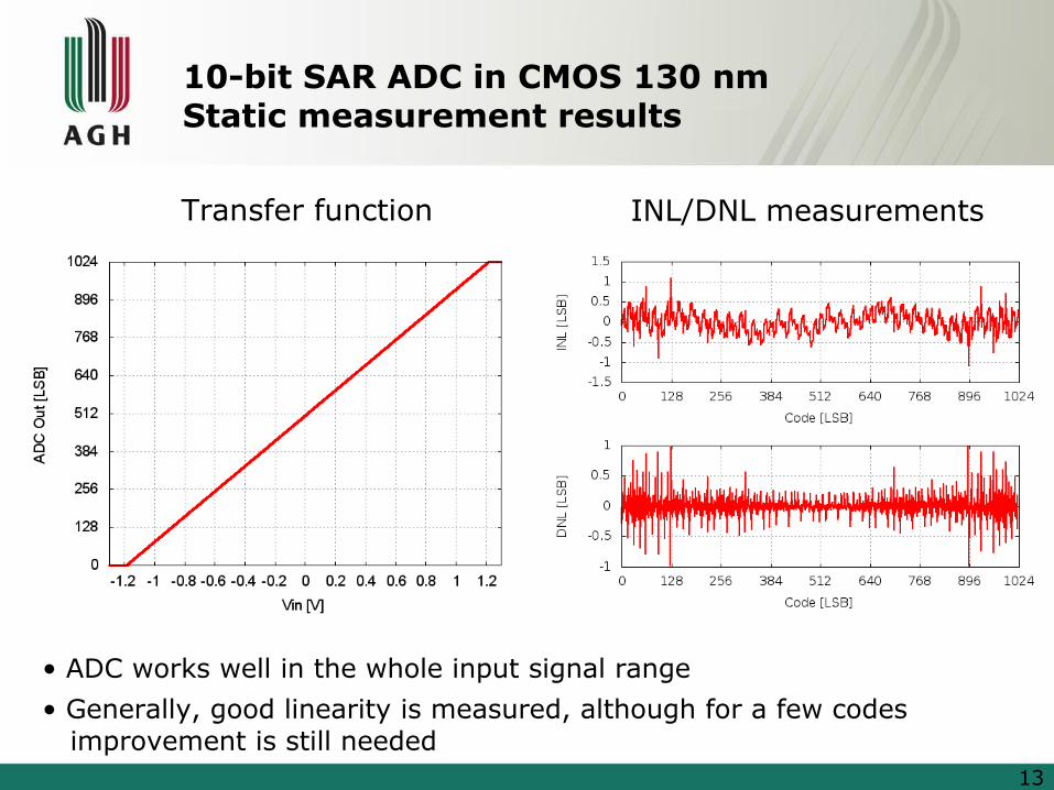
10-bit SAR ADC in CMOS 130 nmStatic measurement results
• ADC works well in the whole input signal range
• Generally, good linearity is measured, although for a few codes improvement is still needed
INL/DNL measurementsTransfer function
14
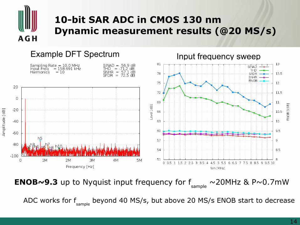
10-bit SAR ADC in CMOS 130 nmDynamic measurement results (@20 MS/s)
ENOB~9.3 up to Nyquist input frequency for fsample
~20MHz & P~0.7mW
Example DFT Spectrum
ADC works for fsample
beyond 40 MS/s, but above 20 MS/s ENOB start to decrease
Input frequency sweep
15
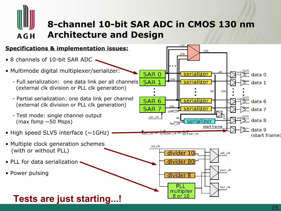
8-channel 10-bit SAR ADC in CMOS 130 nm Architecture and Design
Specifications & implementation issues:
• 8 channels of 10-bit SAR ADC
• Multimode digital multiplexer/serializer:
- Full serialization: one data link per all channels (external clk division or PLL clk generation)
- Partial serialization: one data link per channel (external clk division or PLL clk generation)
- Test mode: single channel output (max fsmp ~50 Msps)
• High speed SLVS interface (~1GHz)
• Multiple clock generation schemes (with or without PLL)
• PLL for data serialization
• Power pulsing
Tests are just starting...!
16
Summary and Future Plans
• New, low power, development of front-end electronics in CMOS 130 nm for LumiCal detector readout at linear collider is proceeding well
– Low power 10-bit SAR ADC has been already positively verified and presented at TWEPP2013,
– 2nd prototype of 8 channel ADC is fabricated and waiting for tests
– 1st prototype of 8 channel analog front-end, shown here, is working well, some quantitive tests (e.g. Cdet dependence) still need to be done...
• We hope to integrate in NEW CMOS 130 nm and submit in 2015 (in one or two ASICs) the whole front-end containing preamp+shaper+ADC in each channel, and all other functionalities (DACs, I2C, PLL, DLL, SLVS) needed in complex SoC type chip
Thank you for attention
17
Testbeam preparationStatus of four boards setup
• Main problems: couplings between boards, noise and disturbances on power and gnd lines
• Old front-end in AMS 0.35um has bad PSRR
• A lot of work was done to optimize existing setup to allow multi-plane operation:
– decoupling, shielding, improved regulators
• Presently the 4-plane setup after improvments behaves not much worse than single board before the changes
• We do not know what will happen after integration in the testbeam area...?