PROGRAMMING BOOK FOR MTK85SE, 8085 MICROPROCESSOR TRAINING KIT · Program 1: Writing data to output...
35
PROGRAMMING BOOK FOR MTK85SE, 8085 MICROPROCESSOR TRAINING KIT Wichit Sirichote © 2016 Rev 1.0 April, 2016 1
Transcript of PROGRAMMING BOOK FOR MTK85SE, 8085 MICROPROCESSOR TRAINING KIT · Program 1: Writing data to output...

PROGRAMMING BOOK FORMTK85SE,
8085 MICROPROCESSORTRAINING KIT
Wichit Sirichote© 2016 Rev 1.0 April, 2016
1

CONTENTS
Program 1: Writing data to output port.................3
Program 2: Binary number counting......................5
Program 3: LED running............................................7
Program 4: Fill constant to RAM..............................8
Program 5: 16-Bit Binary addition..........................10
Program 6: BCD addition..........................................11
Program 7: Reading button press...........................12
Program 8: Producing tone signal..........................15
Program 9: Morse code keyer...................................17
Program 10: 7-Segment display................................20
Program 11: Hardware interrupt.............................24
Program 12: Timer interrupt.....................................26
8085 Micro Architecture
Instruction hex code
2

Program 1: Writing data to output port
We can use debugging LED that connected to GPIO1 port to display the Accumulator content easily. This code will bring the internal 8-bit data in CPU to the real-world.
GPIO1 is 8-bit data flip-flop latch. The GPIO1 latch enable signal, LE is decoded at I/O space location 00.
The output Q1 to Q8 drives small LED. Logic '1' will make LED lit, logic '0' no light.
Let us see how the code brings the Accumulator content to the real-world.
Line Addr Hex code label Instruction
0001 0000 GPIO1 .EQU 00H0002 0000 0003 8100 .ORG 8100H0004 8100 0005 8100 3E 01 START MVI A,10006 8102 D3 00 OUT GPIO10007 8104 FF RST 70008 8105 0009 8105 .ENDtasm: Number of errors = 0
A constant is loaded to the Accumulator register A. Then write it to GPIO1 location. RST 7 will make the program control back to monitor program.
Procedure
1. Enter Hex code from location 8100 to 8104.
3

2. Press key HOME, then GO.
What is happening at GPIO1 LED?
Exercise
1. Modify the code to send another byte? And see the result on GPIO1 LED.
Summary
Using the LED indicator at the output port register is the simple method for program testing. Thekit has 8-bit LED. The byte that needed to check must be loaded into the Accumulator then uses OUT 0, instruction to write it to the 8-bit binary display.
4

Program 2: Binary number counting
How the microprocessor count the 8-bit binary number?
Line Addr Hex code label Instruction
0001 0000 GPIO1 .EQU 00H0002 0000 0003 8100 .ORG 8100H0004 8100 0005 8100 3E 01 START MVI A,10006 8102 0007 8102 D3 00 LOOP OUT GPIO10008 8104 3C INR A0009 8105 C3 02 81 JMP LOOP 0010 8108 0011 8108 .ENDtasm: Number of errors = 0
We modify Program 1 by inserting the instruction INR A and JMP LOOP.
INR A will increment the Accumulator by one.
JMP LOOP will let CPU jump back to address 8102.
Procedure
1. Enter Hex code from location 8100 to 8107.
2. Press key HOME, then STEP.
What is happening at GPIO1 LED when we STEP over location 8102?
We can see the counting in binary from 0000 0000 to 0000 0001, 0000 0010 and so on.
STEP key will let CPU execute single instruction. If we press key GO. What is happening?
All LED will look like turn on, like 1111 1111.
If we try another program by adding a small delay between incrementing.
Line Addr Hex label Instruction
0001 0000 GPIO1 .EQU 00H0002 0000 0003 8100 .ORG 8100H0004 8100 0005 8100 3E 01 START MVI A,10006 8102 0007 8102 D3 00 LOOP1 OUT GPIO10008 8104 3C INR A
5

0009 8105 CD 0B 81 CALL DELAY0010 8108 C3 02 81 JMP LOOP1 0011 810B 0012 810B 11 FF FF DELAY LXI D,-10013 810E 21 00 30 LXI H,3000H0014 8111 19 LOOP2 DAD D 0015 8112 DA 11 81 JC LOOP20016 8115 C9 RET0017 8116 0018 8116 .ENDtasm: Number of errors = 0
Enter the hex code and now press key HOME, GO.
We see that such small delay will make us see the binary counting.
Can you modify the code to make it run faster or slower? How?
Summary
The small delay is very useful subroutine for program debugging. Its functioning is to do counting until the initial value becomes zero.
6

Program 3: LED running
With a bit modification of Program 2, we can show the LED running light with new instruction easily.
Line Addr Hex label Instruction
0001 0000 GPIO1 .EQU 00H0002 0000 0003 8100 .ORG 8100H0004 8100 0005 8100 3E 01 START MVI A,10006 8102 0007 8102 D3 00 LOOP1 OUT GPIO10008 8104 07 RLC0009 8105 CD 0B 81 CALL DELAY0010 8108 C3 02 81 JMP LOOP1 0011 810B 0012 810B 11 FF FF DELAY LXI D,-10013 810E 21 00 20 LXI H,2000H0014 8111 19 LOOP2 DAD D 0015 8112 DA 11 81 JC LOOP20016 8115 C9 RET0017 8116 0018 8116 .ENDtasm: Number of errors = 0
Now, INR A instruction was replaced with RLC, Rotate left through carry.
Procedure
1. Enter hex code from location 8100 to 8115.
2. Press HOME, then GO.
Exercise
1. Modify the initial load value from 1 to any number. Test it.
2. Change running speed faster and slower.
Summary
8085 has left and right rotation instructions. We can learn theirs operation with the GPIO1 LED and with delay subroutine.
7

Program 4: Fill constant to RAM
We will use memory pointer and write the constant with a number of byte counted by loop counter.
Line Addr Hex code label Instruction
0001 8100 .ORG 8100H0002 8100 0003 8100 21 00 90 START LXI H,9000H ; address pointer0004 8103 06 08 MVI B,8 ; loop counter0005 8105 0006 8105 3E 00 MVI A,0 ; constant0007 8107 77 LOOP MOV M,A ; write to memory0008 8108 23 INX H ; next address0009 8109 0010 8109 05 DCR B ; decrement counter0011 810A C2 07 81 JNZ LOOP ; done?0012 810D 0013 810D FF RST 7 ; jump to monitor0014 810E 0015 810E 0016 810E .ENDtasm: Number of errors = 0
The 8085 CPU uses HL as the 16-bit memory pointer (H for High address and L for Low address). The instruction MOV M,A will use HL as the pointer, register A content will copy to memory pointed to by HL. This is called indirect addressing.
Register B uses as the loop counter. The example will write 0 to memory from location 9000H to 9007H, 8 bytes.
Procedure
1. Enter hex code from location 8100 to 810D.
2. Write down the contents of memory location 9000 to 9007.
3. Press key HOME then GO.
4. Check and write down the contents of memory location 9000 to 9007.
Location 9000 9001 9002 9003 9004 9005 9006 9007
Before
After
Exercise
1. Modify code to fill constant FF to location 9000 to 90FF. Show the result.
8

Summary
Indirect addressing using HL register provides a flexible memory access for many applications.
9

Program 5: 16-Bit Binary addition
This program shows how to add multiple bytes using ADI and ACI instructions.
Line Addr Hex label Instruction
0001 8100 .ORG 8100H0002 8100 0003 8100 21 00 90 START LXI H,9000H0004 8103 7E MOV A,M0005 8104 C6 78 ADI 78H0006 8106 77 MOV M,A0007 8107 0008 8107 23 INX H0009 8108 7E MOV A,M0010 8109 CE 9A ACI 9AH0011 810B 77 MOV M,A0012 810C FF RST 70013 810D 0014 810D .ENDtasm: Number of errors = 0
We have two 16-bit numbers to be added.
The first number is stored in memory location 9000 (low byte) and 9001(high byte).
The second number is 16-bit immediate value. 9A78H.
We can enter the first number at location 9000 (low byte) and 9001(high byte).
Adding is done by ADI instruction for low byte and ACI for high byte.
Result will put back to location 9000 (low byte) and 9001(high byte).
Location [9001] [9000]
+ XX YY
9A 78
ADI, add with no carry will use for adding low order byte. For the next higher significant byte we will use ACI, add with carry flag to include carry bit if there is.
Procedure
1. Enter hex code from location 8100 to 810A.
2. Suppose the first number is 1ABBH. Enter it to location 9000(low byte) and 9001(high byte).
3. Compute it by hand, keep the result.
4. Now press key HOME, then GO.
5. Check the result that saved in RAM at location 9000(low byte) and 9001(high byte).
10
Program 6: BCD addition
By inserting DAA instruction after ADI and ACI instructions, we can add two 4-digit BCD numbers easily.
0001 8100 .ORG 8100H0002 8100 0003 8100 21 00 90 START LXI H,9000H0004 8103 7E MOV A,M0005 8104 C6 99 ADI 99H0006 8106 27 DAA0007 8107 77 MOV M,A0008 8108 0009 8108 23 INX H0010 8109 7E MOV A,M0011 810A CE 19 ACI 19H0012 810C 27 DAA0013 810D 77 MOV M,A0014 810E FF RST 70015 810F 0016 810F .ENDtasm: Number of errors = 0
We see that the code for BCD addition is similar to binary addition, only there are DAA after ADI and ACI instruction.
Procedure
1. Enter hex code from location 8100 to 810E.
2. Suppose the first number is 1999H. Enter it to location 9000(low byte) and 9001(high byte).
3. Compute it by hand, keep the result.
4. Now press key HOME, then GO.
5. Check the result that saved in RAM at location 9000(low byte) and 9001(high byte).
Location [9001] [9000]
+ XX YY
19 99
Exercise
1. Try another BCD number that saved in RAM at 9000 and 9001.
Summary
DAA can be used with binary adding instructions. It will adjust the result to BCD number automatically.
11

Program 7: Reading button press
We can test button press with USER key that tied to PA7 of the system PPI, 8255. PA7 is bit7 of PORTA. The input logic appears at PA7 is logic '1' with 10k pull-up resistor. When the button was pressed PA7 will short to GND, the logic will be '0'.
We can read this status by instruction IN PORT directly. The byte will be read to the Accumulator.
Our test program will read key press, then increment the byte at location 9000. We can see theincrementing by writing the content of location 9000 to GPIO1 LED.
Line Addr hex code Label Instruction
0001 0000 PORTA .EQU 10H0002 0000 GPIO1 .EQU 00H0003 0000 0004 8100 .ORG 8100H0005 8100 0006 8100 21 00 90 START LXI H,9000H0007 8103 0008 8103 DB 10 PRESSED IN PORTA0009 8105 E6 80 ANI 80H0010 8107 CA 03 81 JZ PRESSED0011 810A 0012 810A CD 22 81 CALL DEBOUNCE0013 810D 0014 810D DB 10 READ IN PORTA0015 810F E6 80 ANI 80H0016 8111 C2 0D 81 JNZ READ0017 8114 0018 8114 CD 22 81 CALL DEBOUNCE0019 8117 CD 1D 81 CALL WRITE_A0020 811A 0021 811A C3 03 81 JMP PRESSED0022 811D 0023 811D 34 WRITE_A INR M0024 811E 7E MOV A,M
12

0025 811F D3 00 OUT GPIO10026 8121 C9 RET0027 8122 0028 8122 06 00 DEBOUNCE MVI B,00029 8124 05 DELAY1 DCR B0030 8125 C2 24 81 JNZ DELAY10031 8128 C9 RET0032 8129 0033 8129 .ENDtasm: Number of errors = 0
Yellow portions are key press checking. The first one is to wait if key has been pressed. The status of logic at PA7 is checking by logical AND instruction with 80H. Bit position of PA7 is bit 7. Thus we use 80H for bit testing. If logic is '0', Result from logical AND will give ZERO. Thus JZ PRESSED will repeat checking it until it is logic '1', or key has been released.
Logic appears at PA7 could be like this.
Tact switch is mechanical contact. It has elastic property, vibrate in a short period. The logic signal seen by CPU execution would be spike signal. Simple method to get stable logic readings is done by providing a short wait until the logic is stable. We thus insert small delay called DEBOUNCE subroutine.
The second yellow portion is now checking until key was pressed. Again we also get the same bouncing signal but in opposite direction.
So we wait until the logic is stable, then execute the desired task. Our task is to increment location 9000, then write it to GPIO1 LED.
Procedure
1. Enter hex code from location 8100 to 8128.
2. Now press key HOME, then GO.
3. Press USER key, what is happening at GPIO1 LED?
13
Key pressed
Released
Logic '0'
Logic '1'
Logic '0'
Logic '1'
No press
pressed

Exercise
1. Try reduce the delay period.
14

Program 8: Producing tone signal
The kit has one bit that drives a small speaker. We can make a tone signal and hear it from the loudspeaker. Q3 is PNP transistor switch. It can drive the speaker with logic input at SPEAKER signal.
Logic low of SPEAKER signal will turn on Q3, and logic high will turn it off.
We can write a program that makes 50% duty cycle of tone signal.
0001 0000 PORTC .EQU 12H0002 0000 0003 8100 .ORG 8100H0004 8100 0005 8100 3E FF START MVI A,0FFH0006 8102 32 00 90 STA 9000H0007 8105 0008 8105 3A 00 90 TONE LDA 9000H0009 8108 EE 80 XRI 10000000B0010 810A 32 00 90 STA 9000H0011 810D D3 12 OUT PORTC0012 810F 0013 810F 06 20 MVI B,20H0014 8111 05 LOOP DCR B0015 8112 C2 11 81 JNZ LOOP0016 8115 0017 8115 C3 05 81 JMP TONE0018 8118 0019 8118 .ENDtasm: Number of errors = 0
15

Location 9000 stores a byte that will be sent to PORTC. The data is loaded with FF. We see at the circuit of PORTC, the TRACE signal must be HIGH, to prevent TRAP signal to be activated.
Toggle PC7 is done by logical Exclusive OR instruction with a mask byte, 80H or 10000000b.
Small delay is done by register B.
Procedure
1. Enter hex code from location 8100 to 8117.
2. Now press key HOME, then GO.
3. Can you hear the tone signal?
Exercise
1. Modify the delay period to change the tone frequency.
Summary
The output bit at loudspeaker is one bit. So we can make a tone signal as the square wave signal easily. For some applications that produces purely sinusoidal waveform, like sine wave tone signal, we will need more output bits and may need Digital to Analog converter chip.
16

Program 9: Morse code keyer
Let us have some fun with Morse code keyer program. This program combines Program 7 and 8. It is a simple tone generator when we press key.
0001 0000 PORTA .EQU 10H0002 0000 PORTC .EQU 12H0003 0000 0004 8100 .ORG 8100H0005 8100 0006 8100 3E FF START MVI A,0FFH0007 8102 32 00 90 STA 9000H0008 8105 0009 8105 DB 10 PRESSED IN PORTA0010 8107 E6 80 ANI 80H0011 8109 C2 12 81 JNZ READ0012 810C CD 1F 81 CALL TONE0013 810F C3 05 81 JMP PRESSED0014 8112 0015 8112 0016 8112 DB 10 READ IN PORTA0017 8114 E6 80 ANI 80H0018 8116 C2 12 81 JNZ READ
17

0019 8119 0020 8119 CD 30 81 CALL DEBOUNCE0021 811C C3 05 81 JMP PRESSED0022 811F 0023 811F 3A 00 90 TONE LDA 9000H0024 8122 EE 80 XRI 10000000B0025 8124 32 00 90 STA 9000H0026 8127 D3 12 OUT PORTC0027 8129 0028 8129 06 20 MVI B,20H0029 812B 05 LOOP DCR B0030 812C C2 2B 81 JNZ LOOP0031 812F C9 RET0032 8130 0033 8130 0034 8130 06 00 DEBOUNCE MVI B,00035 8132 05 DELAY1 DCR B0036 8133 C2 32 81 JNZ DELAY10037 8136 C9 RET0038 8137 0039 8137 .ENDtasm: Number of errors = 0
We see that while the key has been pressed, tone signal will be produced.
Procedure
1. Enter hex code from location 8100 to 8136.
2. Now press key HOME, then GO.
3. Press key USER and try making Morse code?
Exercise
1. Modify the tone frequency and play again.
Summary
More complicated program can translate the text to Morse code. However it is more fun to learn Morse code and hit the key manually.
18
Here is the Morse code table for playing.
Source: http://rsgb.org/main/operating/morse/
19

Program 10: 7-Segment display
The kit display is made with common cathode 7-segment LED, LTC472. Segment a, b, c, d, e, f, g, DP are driven by PORTB. All segments are common connected to all 8 digits (only 4-digit shown). U12 is segment driver with R9 for limiting driving current. To activate a given digit, the common cathode pin must be activated with logic LOW.
PORTC, PC0 to PC3 drives the 4-bit decoder, 74LS145 providing 8-digit for CC pin driver.
Segment designation for bit driven is shown below. For example, to display number '1', segment B and C must be '1'. The bit pattern will be 03. We can find the bit pattern for a given letter easily.
Such display is called multiplex display. At a given time, only one digit will be activated. However if we switch each digit with corresponding segment fast enough, we will see all digits with no blinking.
20

More features for this circuit, we can use PWM method to reduce the power consumption of the LED thus longer theirs life. We can adjust duty cycle for the driving signal.Here is 50% duty cycle driving pulse.
Smaller duty cycle will reduce power consumption, reduce the LED brightness as well. Proper duty cycle will give nice display with less power.
The first example will display one digit with PWM method.
We will now test the code for single digit display.
0001 0000 SEGMENT.EQU 11H0002 0000 DIGIT .EQU 12H0003 0000 0004 8100 .ORG 8100H0005 8100 0006 8100 3E 7F START MVI A,7FH0007 8102 D3 11 OUT SEGMENT0008 8104 3E F0 MVI A,0F0H0009 8106 D3 12 OUT DIGIT0010 8108 0011 8108 CD 15 81 CALL TIMEON0012 810B 0013 810B 3E 00 MVI A,00014 810D D3 11 OUT SEGMENT0015 810F 0016 810F CD 1C 81 CALL TIMEOFF0017 8112 0018 8112 C3 00 81 JMP START0019 8115 0020 8115 0021 8115 06 01 TIMEON MVI B,10022 8117 05 LOOP1 DCR B0023 8118 C2 17 81 JNZ LOOP10024 811B C9 RET0025 811C 0026 811C 06 64 TIMEOFF MVI B,1000027 811E 05 LOOP2 DCR B0028 811F C2 1E 81 JNZ LOOP20029 8122 C9 RET0030 8123
21

0031 8123 .ENDtasm: Number of errors = 0
Yellow portion will make the first digit to display number '8', code pattern is 7FH.
Time on subroutine makes a turn on period.
Then all segments will be turned off with Time off subroutine for no light period.
Procedure
1. Enter hex code from location 8100 to 8122.
2. Now press key HOME, then GO.
3. Observe the display, see the brightness of the LED.
4 Adjust duty cycle and observe the brightness again.
Exercise
1. Try with another pattern and another digit.
To display all 8 digits, we will use scanning method. 0001 0000 SEGMENT .EQU 11H0002 0000 DIGIT .EQU 12H0003 0000 0004 8100 .ORG 8100H0005 8100 0006 8100 21 26 81 START LXI H,TEXT0007 8103 CD 09 81 CALL SCAN0008 8106 C3 00 81 JMP START0009 8109 0010 8109 0011 8109 ;SCAN DISPLAY 0012 8109 ;ENTRY: HL0013 8109 0014 8109 0E 08 SCAN MVI C,80015 810B 1E 00 MVI E,00016 810D 0017 810D 7B SCAN1 MOV A,E0018 810E F6 F0 ORI 0F0H0019 8110 D3 12 OUT DIGIT0020 8112 0021 8112 7E MOV A,M0022 8113 D3 11 OUT SEGMENT0023 8115 0024 8115 06 01 TIMEON MVI B,10025 8117 05 LOOP1 DCR B0026 8118 C2 17 81 JNZ LOOP10027 811B 0028 811B 3E 00 MVI A,0
22

0029 811D D3 11 OUT SEGMENT0030 811F 0031 811F 1C INR E0032 8120 23 INX H0033 8121 0034 8121 0D DCR C0035 8122 C2 0D 81 JNZ SCAN10036 8125 C9 RET0037 8126 0038 8126 0039 8126 3F TEXT .BYTE 3FH ; '0'0040 8127 06 .BYTE 06H ; '1'0041 8128 5B .BYTE 5BH ; '2'0042 8129 4F .BYTE 4FH ; '3'0043 812A 66 .BYTE 66H ; '4'0044 812B 6D .BYTE 6DH ; '5'0045 812C 7D .BYTE 7DH ; '6'0046 812D 07 .BYTE 07H ; '7'0047 812E 0048 812E 7F .BYTE 7FH ; '8'0049 812F 6F .BYTE 6FH ; '9'0050 8130 77 .BYTE 77H ; 'A'0051 8131 7C .BYTE 7CH ; 'b'0052 8132 39 .BYTE 39H ; 'C'0053 8133 5E .BYTE 5EH ; 'd'0054 8134 79 .BYTE 79H ; 'E'0055 8135 71 .BYTE 71H ; 'F'0056 8136 0057 8136 .ENDtasm: Number of errors = 0
Subroutine scan uses HL as the buffer display pointer.
Register C is number of digit to be scanned.
Register E is digit scan code, which is 0 to 7 for 8-digit.
The example uses 8-byte from 8126 to 812D to be a display buffer.
Procedure
1. Enter hex code from location 8100 to 8135.
2. Now press key HOME, then GO.
3. Observe the display, see the brightness of the LED. And the number being displayed.
4. Change HL to 812E, test it again. See any change?
Exercise
1. Can you show 'HELLO JO' on the display, how?
23

Program 11: Hardware interrupt
The kit provides test button that produces single pulse for interrupt experiment. SW2 is push button, when press and release, the single pulse will send to interrupt pins.
For this test we will select RST6.5, so SW1 must set DIP switch position 2 ON.
0001 8034 .ORG 8034H0002 8034 C3 06 81 JMP SERVICE_RST6.50003 8037 0004 8100 .ORG 8100H0005 8100 0006 8100 F3 MAIN DI0007 8101 3E 0D MVI A,1101B0008 8103 30 SIM0009 8104 FB EI0010 8105 0011 8105 FF RST 70012 8106 0013 8106 SERVICE_RST6.50014 8106 0015 8106 F5 PUSH PSW0016 8107 0017 8107 3E 34 MVI A,34H0018 8109 D3 00 OUT 00019 810B 0020 810B F1 POP PSW0021 810C FB EI0022 810D C9 RET0023 810E 0024 810E .END0025 810E 0026 810E
24

tasm: Number of errors = 0
The interrupt vector for RST6.5 is located at 0034H. The kit relocate this vector to RAM space at location 8034H. User can enter JUMP instruction at 8034H to the service routine for RST6.5 easily.
Since the RST6.5 is a maskable, so to enable it, we must set the mask bit for RST6.5 to '0'. And use instruction SIM to to set it. That is all for main code then the control jump back to monitor program.
When we press test button, the CPU will jump to RST6.5 vector and jump to 8106. The service routine will write a byte 34H to GPIO1 LED. We can see the binary 34H on the GPIO1 LED directly.
Procedure
1. Enter hex code at 8034-8036 for JUMP instruction.
2. Enter hex code from 8100 to 810D.
3. Now press key HOME, then GO.
3. Observe the display, push the test button to produce interrupt signal for RST6.5 pin.
4. Press RESET, observe when push the test button again.
Exercise
1. Modify the code for testing RST5.5 interrupt pin.
25
Program 12: Timer interrupt
The kit provides 33ms tick generated from 8254 timer. The input clock 2MHz supplied to 8254 chip will be divided by 65536 producing 33ms tick. This tick signal is fed to RST7.5.
The monitor program initializes such tick signal at the beginning when reset the CPU. User can use this tick signal for many time trigger applications.
We will play with this tick by RST7.5 interrupt pin. The hardware ties RST7.5 to the output of 8254 directly. No jumper setting needed.
0001 0000 0002 803C .ORG 803CH0003 803C C3 0D 81 JMP SERVICE_RST7.50004 803F 0005 8100 .ORG 8100H0006 8100 0007 8100 F3 MAIN DI0008 8101 3E 0B MVI A,1011B0009 8103 30 SIM0010 8104 FB EI0011 8105 0012 8105 AF XRA A0013 8106 32 00 90 STA SEC_330014 8109 32 01 90 STA SECOND0015 810C 0016 810C FF RST 70017 810D 0018 810D SERVICE_RST7.50019 810D 0020 810D F5 PUSH PSW0021 810E 0022 810E 3A 00 90 LDA SEC_330023 8111 3C INR A0024 8112 32 00 90 STA SEC_33
26

0025 8115 FE 1E CPI 300026 8117 C2 29 81 JNZ SKIP 0027 811A 0028 811A AF XRA A0029 811B 32 00 90 STA SEC_330030 811E 0031 811E 3A 01 90 LDA SECOND0032 8121 C6 01 ADI 10033 8123 27 DAA0034 8124 32 01 90 STA SECOND0035 8127 D3 00 OUT 00036 8129 0037 8129 SKIP 0038 8129 0039 8129 F1 POP PSW0040 812A FB EI0041 812B C9 RET0042 812C 0043 9000 .ORG 9000H0044 9000 0045 9000 SEC_33 .BLOCK 10046 9001 SECOND .BLOCK 10047 9002 0048 9002 0049 9002 .END0050 9002 0051 9002 tasm: Number of errors = 0
Main code initializes RST7.5 mask bit, clear two variables: SEC_33 and SECOND then enable interrupt and return to monitor program.
The RST7.5 service routine will be entered every 33ms or approx. 30 cycles/second.
Every entering, the SEC_33 is incremented by one. When it was equal to 30, time has elapsed for one second. We then increment the SEC variable and write it to GPIO1 LED. We can see the BCD counting up every one second on the GPIO1 LED.
Procedure
1. Enter hex code at 803C-803E for JUMP instruction.
2. Enter hex code from 8100 to 812B.
3. Now press key HOME, then GO.
3. Observe the display. Try pressing keypad as there is no timer interrupt.
4. Press RESET, observe again.
Exercise
1. Change the update rate from one second to 3 seconds.
27

8085 Micro ArchitectureSource: By Appaloosa - Own work, CC BY-SA 3.0, https://commons.wikimedia.org/w/index.php?curid=5217009
28

8085 Instruction Hex Code
29

MOVE, LOAD and STORE
40 MOV B,B41 MOV B,C42 MOV B,D43 MOV B,E44 MOV B,H45 MOV B,L46 MOV B,M47 MOV B,A48 MOV C,B49 MOV C,C4A MOV C,D4B MOV C,E4C MOV C,H4D MOV C,L4E MOV C,M4F MOV C,A50 MOV D,B51 MOV D,C52 MOV D,D53 MOV D,E54 MOV D,H55 MOV D,L56 MOV D,M57 MOV D,A58 MOV E,B59 MOV E,C5A MOV E,D5B MOV E,E5C MOV E,H5D MOV E,L6B MOV L,E6C MOV L,H6D MOV L,L6E MOV L,M6F MOV L,A70 MOV M,B71 MOV M,C72 MOV M,D73 MOV M,E74 MOV M,H75 MOV M,L77 MOV M,A78 MOV A,B79 MOV A,C7A MOV A,D7B MOV A,E7C MOV A,H7D MOV A,L7E MOV A,M7F MOV A,A
3E nn MVI A,byte 06 nn MVI B,byte0E nn MVI C,byte
16 nn MVI D,byte1E nn MVI E,byte26 nn MVI H,byte2E nn MVI L,byte36 nn MVI M,byte
01 nnnn LXI B,dble 11 nnnn LXI D,dble21 nnnn LXI H,dble31 nnnn LXI SP,dble
02 STAX B12 STAX D0A LDAX B1A LDAX D32 nnnn STA adr3A nnnn LDA adr22 nnnn SHLD adr2A nnnn LHLD adrEB XCHG
COMPARE
FE nn CPI byteB8 CMP BB9 CMP CBA CMP DBB CMP EBC CMP HBD CMP LBE CMP MBF CMP A
ROTATE
07 RLC17 RAL 0F RRC1F RAR
STACK
C5 PUSH BD5 PUSH DE5 PUSH HF5 PUSH PSW
C1 POP BD1 POP DE1 POP HF1 POP PSWE3 XTHLF9 SPHL
30

33 INX SP3B DCX SP
ARITHEMATICS
C6 nn ADI byteCE nn ACI byte
80 ADD B81 ADD C82 ADD D83 ADD E84 ADD H85 ADD L86 ADD M87 ADD A88 ADC B89 ADC C8A ADC D
96 SUB M97 SUB A98 SBB B99 SBB C9A SBB D9B SBB E9C SBB H9D SBB L9E SBB M9F SBB A
09 DAD B19 DAD D29 DAD H39 DAD SP
CALL
CD nnnn CALL adrDC nnnn CC adrD4 nnnn CNC adrCC nnnn CZ adrC4 nnnn CNZ adrF4 nnnn CP adrFC nnnn CM adrEC nnnn CPE adrE4 nnnn CPO adr
RETURN
C9 RETD8 RCD0 RNCC8 RZC0 RNZ
F0 RPF8 RME8 RPEE0 RPO
RESTART
C7 RST 0CF RST 1D7 RST 2DF RST 3E7 RST 4EF RST 5FF RST 7
SPECIALS
2F CMA37 STC3F CMC27 DAA
INPUT/OUTPUT
DB nn IN byteD3 nn OUT byte
INCREMENT/DECREMENT
04 INR B0C INR C14 INR D1C INR E24 INR H2C INR L34 INR M3C INR A03 INX B13 INX D 23 INX H05 DCR B0D DCR C15 DCR D 1D DCR E25 DCR H2D DCR L35 DCR M3D DCR A0B DCX B1B DCX D2B DCX H
JUMP
C3 nnnn JMP adr
31
DA nnnn JC adrD2 nnnn JNC adrCA nnnn JZ adrC2 nnnn JNZ adrF2 nnnn JP adrFA nnnn JM adrEA nnnn JPE adrE2 nnnn JPO adrE9 PCHL
LOGICAL
E6 nn ANI byteEE nn XRI byteF6 nn ORI byteA0 ANA BA1 ANA CA2 ANA DA3 ANA EA4 ANA HA5 ANA LA6 ANA MA7 ANA AA8 XRA BA9 XRA CAA XRA DAB XRA EAC XRA HAD XRA LAE XRA MAF XRA AB0 ORA BB1 ORA CB2 ORA DB3 ORA EB4 ORA HB5 ORA LB6 ORA MB7 ORA A
32
55
44
33
22
11
DD
CC
BB
AA
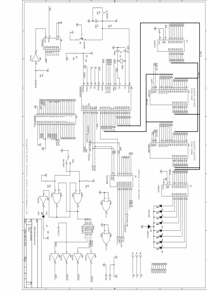
memory & i/o decoder
Designed by Wichit Sirichote, [email protected]
0x8000-0xFFFF32kB SRAM
0x0000-0x7FFF32kB ROM
<Doc>
2
8085 Microprocesor K
it
B
13
Friday, April 15, 2016
Title
Size
Docum
ent Num
berR
ev
Date:
Sheet
of
D1
D0
CLK
OU
T
A14
A9
A0A3D
4
A0
A2A2A7
SO
D
D[0..7]
D0
/RD
D7
A2
A10A11
A12
A8
A14
A12
D5
A6 A5
D5
D5
D3
A4D
4
A8
/RD
D7
A3
D0
D6
D2
A8
A[0..7]
D2
A6
A12
A9
D6
A13
/WR
A13
A1
D2
D7
D0
A10
A4
D1
D2
A[8..14]
D1
A0
D7
D3
D2
D6
ALE
A5
A9
A7
D5
D4
A1A6D
3
D0
D4
D6
D1
D5
D4
RO
M_C
E
A3A5
D6
A14
A13D
1
D7
D3
RAM
_CE
A10
A4A1
A11
A11
D3
A7
A15
A15
IO/M
RAM
_CE
S0
S1
A4A5A6A7
/RD
/WR
ALE
HLD
A
RE
SE
T_OU
T
RO
M_C
E
SID
TRAP
RS
T5.5R
ST6.5
RS
T7.5
INTR
INTA
S0
S1
RE
ADY
SID
D2
D0
D7
D3
D4
GP
IO1
D1
D6
D5
ALE
TRAP
*RS
T5.5R
ST5.5
*RS
T6.5
*INTR
RS
T6.5
RS
T7.5
INTR
D0
D1
D2
D3
D4
D5
D7
D6
/RD
/WR
SID
S0
S1
ALE
IO/M
SO
D
RE
ADY
RE
SE
T_OU
T
CLK
OU
T
*RS
T7.5
A0
*RS
T5.5
A1
HLD
A A3A6
*INTR A7
INTA
A4 A2A5
*RS
T6.5
HO
LD
A0A1A2
GP
IO1
D7
D5
D6
CLK
OU
T
D4
D2
D3
D0
D1
WR
RD
reset
SY
STE
M_P
PI
CTC
US
ER
_PP
IU
ART
LCD
_E
TRAC
E
*RS
T7.5
VCC
VSS
A0A1A2
OU
T1O
UT2
+5V
+5V
+5V
+5V
+5V
+5V
+5V
+5V
+5V
+5V
+5VVC
C
+5V
+5V
D5
D4
JP1
HE
ADE
R 20X
2
12
34
56
78
910
1112
1314
1516
1718
1920
2122
2324
2526
2728
2930
3132
3334
3536
3738
3940
D3
LED
3mm
R3
10k
D2
R6
10k
D91N
5237A
D1
U9
74HC
164
1289
345610111213
ABCLK
CLR
QA
QB
QC
QD
QE
QF
QG
QH
U5
GAL16V8B
111
1213141516171819
23456789
I/CLK
I/OE
I/O/Q
I/O/Q
I/O/Q
I/O/Q
I/O/Q
I/O/Q
I/O/Q
I/O/Q
IIIIIIII
U7A
4001
123
Q2
KIA7042
1
2
3
U7B
4001
564
SW
2
SW
SP
DT
123
U4
74HC
573
1 1120
1918171615141312
23456789
OE
LEVCC
1Q2Q3Q4Q5Q6Q7Q8Q
1D2D3D4D5D6D7D8D
+C
310uF
U1
27C256
109876543252421232262720221
1112131516171819
A0A1A2A3A4A5A6A7A8A9A10A11A12A13A14
CE
OE
VPP
O0
O1
O2
O3
O4
O5
O6
O7
U2
HM
62256B
109876543252421232261202227
1112131516171819
A0A1A2A3A4A5A6A7A8A9A10A11A12A13A14
CE
OE
WE
D0
D1
D2
D3
D4
D5
D6
D7
U6
MS
M80C
85A
361256987101129333935
1213141516171819212223242526272830313234337438
RS
T-IN
X1
X2
SID
TRAP
RS
T 5.5R
ST 6.5
RS
T 7.5
INTR
INTA
S0
S1
HO
LD
RE
ADY
AD0
AD1
AD2
AD3
AD4
AD5
AD6
AD7A8A9
A10A11A12A13A14A15
ALEW
RR
DIO
/MR
ST-O
TC
LKO
SO
DH
LDA
SW
1
SW
DIP
-4
1234
8765
U8F
74LS14
1312
U7C
4001
8910
U7D
4001
121311
R1
10k
U8E
74LS14
1110
R2
100
R4
10k
R510k
U8A
74LS14
12
R8
10k
D10
LED
Q1
4MH
z
U8B
74LS14
34
U8C
74LS14
56
R7
330
U8D
74LS14
98
S1
RE
SE
T
D8
C1
30pF
D7
C2
30pF
U3
74HC
573
1 1120
1918171615141312
23456789
OE
LEVCC
1Q2Q3Q4Q5Q6Q7Q8Q
1D2D3D4D5D6D7D8D
D6

55
44
33
22
11
DD
CC
BB
AA
GO INC
0 4 8 CD951
DEC
ALT
EA62
STEP
ADDR
FB73
HOME
DATA
USER1
MODE
OPTION
<Doc>
2
8085 Microprocesssor K
it
B
23
Friday, April 15, 2016
Title
Size
Docum
ent Num
berR
ev
Date:
Sheet
of
CDG EF ADP
BCG ED
P
BF D AP
B0
PB
1
PB
3P
B2
PB
5P
B6
PB
7
PB
4
PC
0
PC
3
PC
1P
C2
PB
0P
B1
PB
2P
B3
PB
5P
B4
PB
7P
B6
PA0
PA3
PA7
PA6
PA1
PA2
PA4
PA5
PC
5
PC
0
PC
3P
C2
PC
7
PC
4
PC
1
SP
EAK
ER
PC
6
PA5
PA2
PA6
PA3
PA7
PA0
PA1
PA4
D6
D3
D2
D1
D4
D7
D0
D5
A1A0
D1
D6
D3
D7
D4
D2
D5
D0
A0A1A2 SP
EAK
ER
PA6
PA7
US
ER
TRAC
E
VSS
VCC
SY
STE
M_P
PI
reset
WR
RD
D0
D7
D5
D2
D4
D3
D1
D6
A0A1A2
VCC
+5V
VCC
VCC
+5V
U11
LTC-4727JR
1416133511157
1
2
6
8
4
ABCDEFGDP
DIGIT1
DIGIT2
DIGIT3
DIGIT4
L1L2L3
SW
8
12
SW
13
12
SW
3
12
SW
17
12
R9
R-P
ACK
116
215
314
413
512
611
710
89
SW
14
12
SW
15
12
SW
16
12
R1210
LS1
SP
EAK
ER
SW
25
12
SW
22
12
SW
23
12
SW
26
12
SW
12
12
U12
74LS244
246811131517119
181614129753
1A11A21A31A42A12A22A32A4
1G2G
1Y1
1Y2
1Y3
1Y4
2Y1
2Y2
2Y3
2Y4
SW
24
12
SW
9
12
U13
74LS145
15141312
123456791011
ABCD
0123456789
U14
8255
34 33 32 31 30 29 28 27 5 36 9 8 35 6
4 3 2 1 40 39 38 37 18 19 20 21 22 23 24 2514 15 16 17 13 12 11 10
D0
D1
D2
D3
D4
D5
D6
D7
RD
WR
A0 A1 RE
SE
TC
S
PA0
PA1
PA2
PA3
PA4
PA5
PA6
PA7
PB
0P
B1
PB
2P
B3
PB
4P
B5
PB
6P
B7
PC
0P
C1
PC
2P
C3
PC
4P
C5
PC
6P
C7
SW
10
12
SW
27
12
SW
11
12
SW
28
12
D11
TON
E
C
R13
10k RE
SIS
TOR
SIP
91
23456789
R104.7k
SW
29
12
SW
21
12
R11
330
SW
18
12
SW
7
12
SW
19
12
SW
4
12
SW
5
12
SW
20
12
Q3
BC
557
1
2
3
SW
6
12
U10
LTC-4727JR
1416133511157
1
2
6
8
4
ABCDEFGDP
DIGIT1
DIGIT2
DIGIT3
DIGIT4
L1L2L3

55
44
33
22
11
DD
CC
BB
AA
RS R/W
16x2 text LCD interface
<Doc>
2
8085 Microprocessor K
it
B
33
Friday, April 15, 2016
Title
Size
Docum
ent Num
berR
ev
Date:
Sheet
of
D5
D6
D4
D7
D0
D3
D2
D1
D1
D6
D7
D0
D2
D5
D4
D3
D[0..7]
A0A1
A0A1A2
A0A1A2R
XD
TXD
RTSD
CD
RTS
DC
D
D7
D0
D3
D2
D1
D4
A0
D6
A1
D5
DC
2
D1
D3
D4
D0
D6
D7
D2
D5
RD
WR
CTC
CLK
OU
T
VCC
VSS
*RS
T7.5
A0A1A2
RD
WR
reset
UAR
T
RX
D
TXD
LCD
_EO
UT1
OU
T2
D4
D5
D6
D1
D3
D0
D7
D2
VCC
+5V
+5V
+5V
+5V
+5V
+5V
VCC
+5V
+5V+5V
+C
1110uFC
180.1uF
C16
0.1uF
D13
1N4007
12
+C
12
10uF 16V
C15
0.1uF
+
C5
10uF
VB1
SU
B-D
9, Male (cross cable)
594837261
+
C4
10uF 10V
U16
8254
876543212223192021
91110151413181617
D0
D1
D2
D3
D4
D5
D6
D7
RD
WR
A0A1CS
CLK
0G
0O
UT0
CLK
1G
1O
UT1
CLK
2G
2O
UT2
C19
0.1uF
U15
8250
1213142118221928272612345678253516179
343130113233103837363924232915
CS
0C
S1
CS
2
RD
WR
RD
WR
A0A1A2D0
D1
D2
D3
D4
D5
D6
D7
ADS
RE
SE
T
XTAL1/C
LKX
TAL2
RC
LK
OU
T1O
UT2
INT
TXD
RTS
DTR
RX
DD
CD
DS
RC
TSRI
CS
OU
TD
DIS
NC
BAU
DO
UT
C17
0.1uF
J1D
C input
1
2
JR1
CO
NN
RE
CT 16
1 2 3 4 5 6 7 8 9 10 11 12 13 14 15 16
1 2 3 4 5 6 7 8 9 10 11 12 13 14 15 16
+
C6
10uF
R14
5
C20
0.1uF
C8
100nF
R16
2k
C9
100nF
TP1
+5V1
+
C7
10uF R15
10K
13
2
D12
PO
WE
R
U17
MAX
232A
138
1110 1345
26
129
147R
1INR
2IN
T1INT2IN C
+C
1-C
2+C
2-
V+V-
R1O
UT
R2O
UT
T1OU
TT2O
UT
C14
0.1uF
TP2
GN
D1
+C
131000uF 16V
U18
LM7805/TO
1
2
3VIN
GND
VOU
T
+C
1010uF