Programmer Electronic Control - Command Set€¦ · adding and Programmer Electronic Control...
17
Programmer Electronic Control - Command Set - Reverse-Engineering and restoration Project 2005-2009 by Dr. Erik Baigar, [email protected] Revision 2009/04/10 All Rights Reserved and Description 0 0 0 0 LDI-Group: Data from memory position is transferred to index register . Next Operation of STA, STS, INC, ADD and SUB occurs relative to this index register. Afterwards is cleared by these instructions. The index register is always loaded from the zero-page if (LDI). The LDIP instruction with uses the page register to calculate the adress via . The unit freezes during memory access and needs power cycle to recover if P is not initialized before using the LDIP instruction. 0x000, 0, Function 0, 0 0 0 1 ADD-Group: Data from memory position is ADDed to accumulator and result is stored within accumulator (ADD, ). is cleared during adding and Programmer Electronic Control freezes if (ADDP) in an attempt to access a not initialized page register . Address calculation as in LDI. There seems to be no carry flag mechanism during addition. 0x100, 256, Function 1, 0 0 1 0 SUB-Group: Accumulator is subtracted from data in memory location . Result is kept in the accumulator register, set to zero after the in- struction. SUBP uses the above mentioned paging register and the CPU freezes in SUBP ( ) in encountering an uninitializted register. No carry mechanism discovered so far. 0x200, 512, Function 2, 0 0 1 1 STS/STB-Group: Stores the register 1 to core memory . is used for relative memory access and cleared after this access. Accumulator remains unchanged. The register is implemented on the data boards SK8 and SK9 and is used in SHR, SHL, MUL and DIV commands - see below. Bit7 switches the paging mechanism: STB for without paging and STBP if with paging (ad- dress calculated as in ADD above). The unit freezes on STBP if is not initialized! Waveform-Example sta0_clr129_sta2: NRESET RESET AAD[11:0] NAD[11:0] 7MEMCK 7MEMRD 7MEMWR fff f5e fff c7e fff 57e fff f5d fff afd fff ffd fff 0a1 381 a81 0a2 502 002 6000 7200 8400 9600 10800 6408 9392 2984 0x300, 768, Function 3, 1 Early during investigation this was called ¨ extended shifter register¨ , thus the assembler understands the old STS
Transcript of Programmer Electronic Control - Command Set€¦ · adding and Programmer Electronic Control...

Programmer Electronic Control- Command Set -
Reverse-Engineering and restoration Project2005-2009 by Dr. Erik Baigar, [email protected]
Revision 2009/04/10All Rights Reserved
����� ����� ��� ��� ��� � ����� and Description
0 0 0 0
LDI-Group: Data from memory position� ����� � ��� ��� is transferred to index register�����
. Next Operation of STA, STS, INC, ADD and SUB occurs relative to thisindex register. Afterwards
�����is cleared by these instructions. The index register
is always loaded from the zero-page if � ���� (LDI). The LDIP instruction with� �"! uses the page register # to calculate the adress via !%$'&�( #*) ����� )*+ ����� � ��� �-, .The unit freezes during memory access and needs power cycle to recover if P is notinitialized before using the LDIP instruction. 0x000, 0, Function 0, .�/ 0 ���21�3
0 0 0 1
ADD-Group: Data from memory position� ����� ) ����� � ��� ��� is ADDed to accumulator
and result is stored within accumulator (ADD, �� �4� ) .�����
is cleared duringadding and Programmer Electronic Control freezes if � 5�6! (ADDP) in an attemptto access a not initialized page register # . Address calculation as in LDI. There seemsto be no carry flag mechanism during addition. 0x100, 256, Function 1, .�/ 7 � 0 1�3
0 0 1 0
SUB-Group: Accumulator is subtracted from data in memory location� ����� )� � � � ���8� � . Result is kept in the accumulator register,
�����set to zero after the in-
struction. SUBP uses the above mentioned paging register # and the CPU freezes inSUBP ( � 9�:! ) in encountering an uninitializted # register. No carry mechanismdiscovered so far. 0x200, 512, Function 2, 7�/ ;�;20 1�3
0 0 1 1
STS/STB-Group: Stores the < register1 to core memory� ����� ) ��-� � ��� ��� . ����� is
used for relative memory access and cleared after this access. Accumulator remainsunchanged. The < register is implemented on the data boards SK8 and SK9 and isused in SHR, SHL, MUL and DIV commands - see below. Bit7 switches the pagingmechanism: STB for � =�6� without paging and STBP if � =�>! with paging (ad-dress calculated as in ADD above). The unit freezes on STBP if # is not initialized!Waveform-Example sta0_clr129_sta2:
NRESET
RESET
AAD[11:0]
NAD[11:0]
7MEMCK
7MEMRD
7MEMWR
fff f5e fff c7e fff 57e fff f5d fff afd fff ffd fff
0a1 381 a81 0a2 502 002
6000 7200 8400 9600 10800
6408 9392
2984
0x300, 768, Function 3, .�/ ��� . 1�31Early during investigation this was called ¨ extended shifter register¨ , thus the assembler understands the old STS

� ��� � ��� � � � � � � � ��� � and Description
0 1 0 0
LDA-Group: With � �"� (LDA) the accumulator register is loaded from memorylocation
� ����� ) � � � � ����� � and the < register is unmodified by this instruction.�����
is cleared by the LDA operation and PEC switches paging on if � � ! (LDAP).Adress is calculated as followd for paging on: !%$'&�( #") ����� ) + ����� � ��� � , . PECfreezes if � � ! (LDAP) in an attempt to access a not initialized page register # .
0x400, 1024, Function 4, .�/ 7 � . 1�3
0 1 0 1
STA-Group: The accumulator register is stored in memory location� ����� ) � ��� � ��� ���
and the accumulator is not affected by the instruction.�����
is cleared by theSTA/STAP operation and PEC freezes if a STAP ( � �� ! ) is used and # has notbeen initialized before. Signals during STA:
NRESET
RESET
AAD[11:0]
NAD[11:0]
7MEMCK
7MEMRD
7MEMWR
f5f fff aff fff f5e fff cfe fff
0a0 500 0a1 301
2400 3600 4800 6000 7200
3524 6499
2975
0x500, 1280, Function 5, .�/ � � ; 1�3
0 1 1 0
AND-Group: The accumulator register logically ANDes with memory location� ����� ) �8�-� � ��� � � . ����� is cleared by the AND/ANDP operation and PEC calcu-lates the address from !%$'& ( # ) ����� ) + � � � � ���8� , if paging is activated in ANDP( � � ! ).
0x600, 1536, Function 6, .�/ 7 � 1�3
0 1 1 1
RJAZ-Group: Continues with next instruction immediately if accumulator is notzero. Otherwise the RJAZ instruction (Relative-Jump-if-Accu-Zero) performs a re-lative jump like RJMP.
0x700, 2047, Function 7,� / � � � .�/ � . � 1�3
as well as the new STB.
� ��� � ��� � � � � � � � ��� � and Description
1 0 0 0
RJMP-Group: � determines wether the jump is � ��� � ��� � instructions forward ( � =0)or backward ( � =1). Especially 100000000000 and 100010000000 are the same re-presentation of a loop lasting forever.
NRESET
RESET
AAD[11:0]
NAD[11:0]
7MEMCK
7MEMRD
7MEMWR
f5f fff 7f5 fff f55 fff 775 fff f5f fff 7f5 fff
0a0 80a 0aa 88a 0a0 80a
2400 3600 4800 6000 7200
3496 5261
1765
Special care has to be taken if�����
is not zero. In this case the jump width is calcu-lated in the following way: + � ! ,�� � �� � ����� ) ����� � ��� ��� and IDX is cleared by thejump. 0x800, 2048, Function 8,
� / � �21�3
1 0 0 1
RJAN-Group: Continues with next instruction immediately if accumulator is positi-ve, i.e. � ��� � � . Otherwise the RJAN instruction (Relative-Jump-if-Accu-Negative)performs a relative jump like RJMP. 0x900, 2304, Function 9,
� / � 7 1�3
1 0 1 0
INC-Group: The accumulator register is loaded from memory location� ����� ) �8��� � ��� ��� (INC, paging off for � � � ) or from� !%$'& ( # ) ����� ) + �8��� � ��� � ,��
(INCP, paging active for � � ! ). Then the accumulator incremented and the resultis stored back to the same address.
�����is cleared after the INC’s write operation
and PEC freezes in INCP if the page register # has not been initialized after bootingthe PEC. Especially remember, that INC modifies the accumulator!
0xa00, 2560, Function 10, 7�/ � � � 1�3
1 0 1 1
IDXCALL-Group: First, the memory location of the next instruction to execute (i.e.# � ) ! ) is saved to the memory adress specified in the lower 7 bits of the command:# � ) !�� � � � � � � � � � ��� ��� (In case of the IDXCALLP the the paging is used only inthis step, i.e. # � ) !�� � !%$'&=( # ) � � � � � � � � ��� ��� . If # is not initialized here, PECwill freeze!).Afterwards the new program counter # �is loaded from the memory location where�����
points to, i.e. the execution is continuedwith an indirect jump (
� ����� � � # � ,here no paging is used.). Adresses arestored/read in two successive words withMSW ( �'�'� � � . �'�'�'�'�'�'�'� ) first and than LSW( � ��� � � � � � ). In case of the paging variantIDXCALLP, the MSW of the return addresscontains the current value of the pagingregister ( �'�'� � � . � � � � ). The accumulatorregister is not affected by this operation and�����
is cleared. This operation can jump thethe upper half of the memory without free-zing the unit and < and # are not influenced2 .
IDXCALL AdrPC IDX
AdrAdr+1
IDXIDX+1
.
.
.
WritecurrentPC+1
000 pc12 00000000pc11 ........ pc0
.
.
.
000 Npc12 00000000Npc11 ....... Npc0
GetnewPC
.
.
.
NPC
Continue Operationat NPC
0xb00, 2816, Function 11,� / � � 1�3
2This indeed remarkable, since the � is written together with the current address but it is NOT read in reading thedestination address!

� ��� � ��� � � � � � � � ��� � and Description
1 1 0 0
UMUL-Group: This command multiplies the accumulator with the value read from� ����� ) � � � � ����� � . Using the paging variant UMULP (for �� � ! ), the address iscalculated including the # and the
�����registers as usual. The unit freezes in exe-
cuting an UMULP if # has not been initialized. This multiplication is executed inmicrocode and incorporates 12 shift and add operations. Therefore the multiply lastsfor more than & � &���� . IDX operates as usual. The result is stored in the < 3 register(LSW, i.e. ��� ����� � � � � ) and the accumulator (MSW, ��� . � � � � � ��� ).Caution: Only positive numbers (i.e. with bit 11 zero) are multiplied correctly. ThusUMUL and UMULP essentially are 11bit * 11bit multiplications. IDX is cleared bythe operation and the special shift register is cleared before the multiply process.
0xc00, 3072, Function 12,� / 7 � �21�3
1 1 0 1
UDIV-Group: Iteratively executes a division. Herein the 22bit value formed by Accuand < is divided by the memory operand and the result is stored in the accumulatorregister:
� ��� � � � � � ����� /�/�/ ���� ��� /�/�/ �� �� /�/�/ � �< is invalid after the operation (especially it does NOT give the reminder of theoperation). The address of the memory operand is calculated according to the pagingmechanism: For UDIV (specified by � � � ) paging is disabled and the address isgiven by
����� ) � � � � ����� . For the paging UDIVP (for �� � ! ) the address is givenby !%$'& ( # ) ����� ) �8��� � ��� � . The paging variant freezes if # has not been initializedsince powering up the unit.
0xd00, 3382, Function 13,� / � ;�. 1�3
3 � is the same as the special shift register in previous versions of this document since this register was discoveredduring investigating shift operations.

� ��� � ��� � � � � � � � ��� � and Description
1 1 1 0
Special-Group: Depending on � � � ��� � special functionality is available:� �8� � ; � 0 � � ��� � and Description
0 0 0
SHL: Shifts accu left by � 0 � � ����� bits. Instruction takes +�� )� 0 � � ��� � , -MEMEN/AADEN2-Cycles to complete. In each shiftcycle first accumulator is shifted left where the MSB is dropped.Afterwards on the right side of accumulator � ��� of the < register(extended shift register) is inserted for � � . Afterwards < is shiftedleft as well where the LSB is cleared: � � � � . The extended shiftregister < can be accessed via the STB instruction.
0xe00, 3584, Function 14-0-0, .�/ � . �21�3��5� / ; � 1�3����
0 0 1
� 0 � 7 � . � � � - MSRTA/MBTA: Regardless of � 0 � 7 � . � �Moves the < register to the Accumulator4 . All 16 possibleopcodes encode the MBTA instruction. Additionally, if
�����has been set prior to MBTA then the following actions occur:(1) B:= + ������� ! ,(2) Akku:= + �������� ! ,
0xe20, 3616, Function 14-0-32, .�/ 7�7 � 1�3
0 0 1
� 0 � 7 � . ��� ! - RSIDXTA: R ight Shift IDX to Accumulator(16 possible bit patterns): With
�����set prior to RSIDXTA the
following operations are executed:(1) B:= + ������� ! , and(2) if
�����odd then Akku:= + �������� ! , otherwise Akku un-
changed.0xe21, 3617, Function 14-0-33, .�/ 7 � �21�3
0 1 0
� 0 � 7 � . � � � - MPTA - Move # to Accu: Regardless of � 0 � � ��� �the lower byte of the Accu is read back from the page register # .
0xe40, 3648, Function 14-0-64, .�/ 720 �21�3
0 1 0
� 0 � 7 � . ��� ! - MTA: This instruction makes a second core readcycle at the next program counter address and reads this to theaccumulator register. Regardless of � 0 � 7 � . � � this is done, i.e.16 possible bit patterns exist for this instruction and this is theonly two-cycle-instructionof the unit! (Move to Accumulator.)
0xe41, 3649, Function 14-0-65, .�/ � � 0 1�3
0 1 1
SHR: Shifts accu right by - � 0 � � ��� � bits (i.e. � 0 � � ��� � � !'!'!'!'!shifts right one bit). Instruction takes +���)� + � 0 � � ��� � , ) ! , -MEMEN/AADEN2-Cycles to complete. First the extended shiftregister ( < ) which can be accessed by the STB instruction is shif-ted right one position where it’s � � bit is lost. Afterwards the ac-cu is shifted right and therein � ��� is replicated to � ��� . The bit � �which is shifted out of accumulator is inserted as � ��� into < . Thusthere exist 11 hidden bits in the shifter unit’s extended shift regi-ster < : � ��� � � � � � .
0xe60, 3680, Function 14-0-96, .�/ � . �21�3��5� / ; � 1�3����
4Earlier this instruction was called MSRTA as a acronym for Move the extended Shift Register to the Accumulator.But since the extended shift register is now � , the instruction has been changed. Old instruction still supported forcompatibility.

� ��� � ��� � � � � � � � ��� � and Description
1 1 1 0
Special-Group: Depending on � � � ��� � special functionality is available:
1 0 0
Does an IOR instruction to address ! � � 0 � � ���8�(EMUX=EMUXA=EMUXB=1) where the accumulator ismodified.
0xe80, 3712, Function 14-1-0, 0 / � 2�21�3
1 0 1
MATSR/MATB: Completely independent of � 0 � � ��� � this instruc-tion Moves the Accumulator to < , the extended shift register5.All 32 possible combinations encode the MATB instruction!
0xea0, 3744, Function 14-1-32, .�/ 720�0 1�3
1 1 0
MATP with � 0 � � ��� � � is a single word instruction copying the cur-rent value of the accumulator to the page register # . After thisoperation, the paging instructions can be used without freezingthe PEC. Adress is calculated in all these instruction according tothe following formula, whereas
�����is cleared in each instructi-
on and # is persistent: !%$'& ( # ) ����� ) + ���� � ��� � , .0xec0, 3776, Function 14-1-64, .�/ � 7 �21�3
1 1 0
MTP with � 0 � � ��� � � is a dual word instruction loading the wordfollowing the command to the page register # . After this operati-on, the paging instructions can be used without freezing the PEC.Adress is calculated in all these instruction according to the fol-lowing formula, whereas
�����is cleared in each instruction and
# is persistent: !%$'& ( # ) ����� )"+ ��-� � ��� �-, . No other registersare affected.
0xec1, 3777, Function 14-1-65, 7�/ ;�7 �21�3
1 1 1
IRQack: Acknowledge interrupt and write interrupt mask regi-ster: � 0 � � ���8� has the following meaning:
Bit Action� 0 1: Enable IRQ for DPL2.� 7 1: Enable IRQ for DPL3.� . 1: Enable IRQ for DPL1.��� 1: Enable IRQ for DPL4.� � 1: Global IRQ enable and ack current IRQ.Does not alter the accumulator or the extended shift register.
0xee0, 3808, Function 14-1-96, ;�/ ��� 1�3
5Historcally this was the MATSR instruction: Moves the Accumulator to extended Shift Register. It is supported forcompatibility, but in the future it should be replaced by MATB since the registers are called � , � , ����� and � fromnow on.
� ��� � ��� � � � � � � � ��� � and Description
1 1 1 1
IOR-Group: Data is read from the IO modules. � 0 � � ��� � is some kind of addresswhich is applied to the bus in an intermediate state:
0 x y 0
The read commands first send a header out via the correspondingfast link:
Output due to reading:
1 ParamLSB0
ParamMSB3
Id0
Id1
01
After terminating this by a clock high phase PEC waits up to � � ���for a packet being received (12 bits, LSB first, also terminatedby clk high for 2 cycles). Afterwards PEC reads the contents ofthe fast serial link’s input and continues operation. � 7 � � ��� � aretransmitted within the header as address as well as the plug-index(see WDPL commands).// Some instructions code the internaltimer and DPL05 registers and PEC will only wait for an incomingpacket, if the inbound clk is at low level during the RDPLcommand:
DPL � � Command01 0 0 RDPL1 � 7 � � ��� � +��� �'�'� ��� 0:ppt � 1:tty ,02 0 1 RDPL2 � 7 � � ��� � +��� !'!'!'! � timer ,03 1 1 RDPL3 � 7 � � ��� �04 1 0 RDPL4 � 7 � � ��� � +��� �'�'� ! � �� �'�'�'� � DPL05 ,
Waveform seen on the outbound channel in RDPL1 2:
Function 15-0-(2-15,32-46,64-79,98-111), 0 / � ��� 1�3 � 7 � / �����21�3
0 x y 1
Yet unknown command - internally performs an IOR cycle to theaddress given by the parameter.
Function 15-0-(16-31,48-63,80-95,112-127), 0 / � ��� 1�3

� ��� � ��� � � � � � � � ��� � and Description
1 1 1 1
IO-Group2: Accesses the internal timer module and the seperate 24 bit transceivermodule for DPL05. Listed seperately despite the commands beeing integral part ofthe IOR and IOW module. This is for clarity. DPL05 operates at a data rate of $��������per bit (3.906kBaud) and the timer has tic period of one per ��� .
0 0 0
RPPT: + � 0 � � ����� � �'�'�'�'��, Gets the next value from paper tapeinto accumulator; Caution: PEC is waiting until the word has beenloaded, even if no paper tape is connected. Reset works in thissituation.
0xf00, 7400, Function 15-0-0, variable
0 0 0
RTTY: + � 0 � � ��� �5� �'�'�'� ! , Reads a word into accumulator; Cau-tion: PEC is waiting until the word has been transferred. WithoutTTY PEC is waiting indefnitely, but Reset recovers PEC.
0xf01, 7401, Function 15-0-1, variable
0 0 1
MTTA: + �8��� � ��� � �4� !'!'!'!'!'! , Loads the accumulator with thecurrent value of the timer.
0xf3f, 7477, Function 15-0-63, 0 / .�; � 1�3
0 1 0
RDPL5H, RDPL5L: Reads the current values of the shift regi-sters into the accumulator. Transmission has to be controlled byinterrupt routine: Only there these registers should be accessed.
0xf4(0,1), 750(0,1), Function 15-0-(64,65), .�/ � � 1�3
1 0 0
WPPT: + � 0 � � ����� � �'�'�'�'��, Write accumulator to paper tape andwait for acknowledge from paper tape. Prolonged waiting mayoccur, especially without paper tape connected.
0xf80, 7600, Function 15-1-0, variable
1 0 0
WTTY: + � 0 � � ��� � � �'�'�'� ! , Write current contents of the accu-mulator to TTY. PEC is waiting until the word has been trans-ferred and without TTY connected to PEC waiting is indefnitely.Reset ca terminate this state.
0xf81, 7601, Function 15-1-1, variable
1 0 1
MATTC: + �8��� � ��� � � � !'!'!'!'!'! , Stores the accumulator into thethe timer’s 12 bit comparator register for the internal timer of thePEC. A counter is counting upwards until it reaches the valuespecified in the comparator register. This counter is incrementedevery &���� , leading to approx. 32ms maximum interval betweeninterrupts.On occurence of an interrupt, the program execution is interrup-ted, the current address is saved to memory 0x00 (high bit, pageregister) and 0x001 (low word) and execution continues at the ad-dress specified by 0x84, 0x85.
0xfbf, 7677, Function 15-1-63, 7�/ � .20 1�3
1 1 0
WDPL5H, WDPL5L: Write the accumulator the the DPL05’stransmitter registers. High + ����� � ��� � � �'�'�'�'� ! , and low+ �8��� � ��� � � �'�'�'�'�'��, word have to be written seperately and theMSB of MSW is automatically set to 1 during write. Unclear howtransmission is started (needs more than one write) and the LSBof LSW is sent first. This bit is present during the clock pausebefore each transmission.
0xfc(0,1), 770(0,1), Function 15-1-(64,65), 0 / 0 ; � 1�3
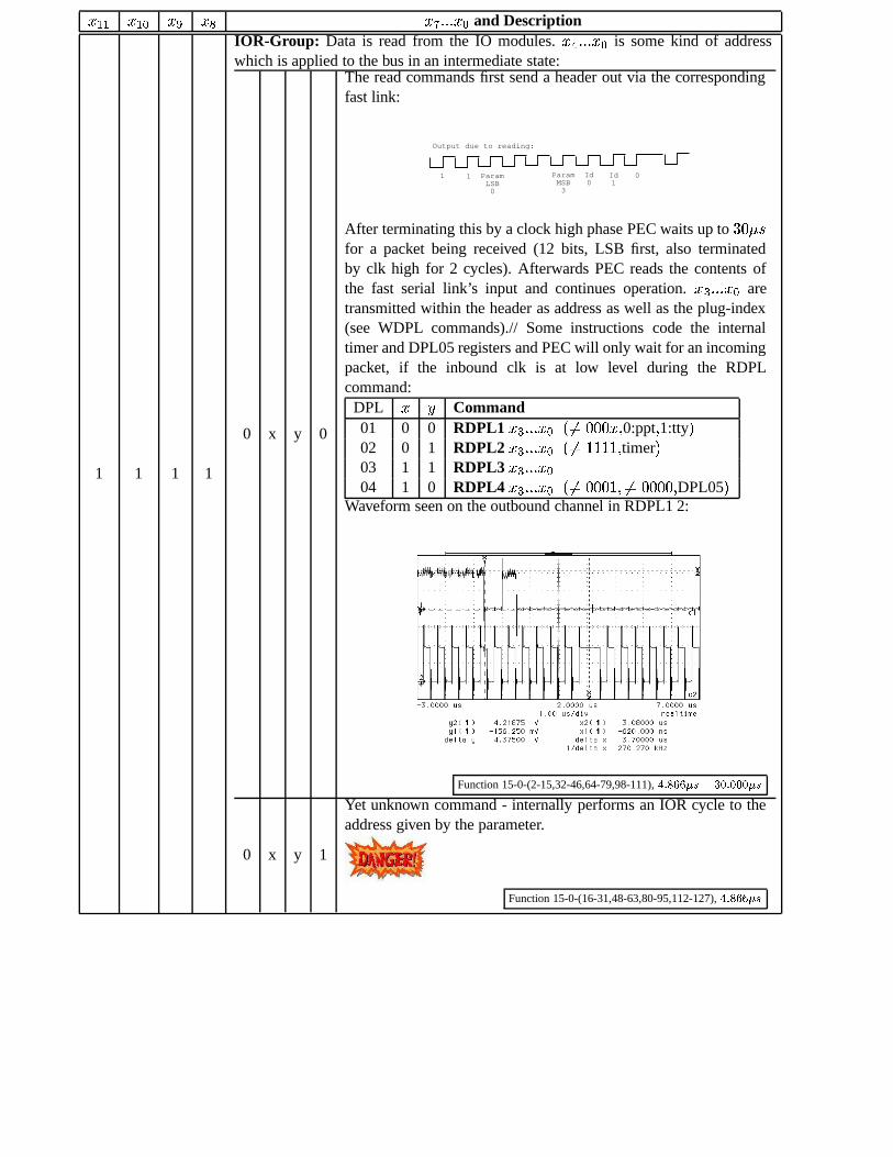
Waveforms during transmission on DPL05: Top channel is the clock signal which is running all the time(except reset and DMA state). Lower trace shows the data signal. Only during the first 24 clock cycles data
is transmitted:
During the pause on the clock signal when it is high, the lowest bit of the transmitter is directly visible onthe output. Thus writing the transmit register continuously leads to the bursts visible on the data line in the
clock pause.
Still unknown how to determine, when the transmission has completed.
� ��� � ��� � � � � � � � ��� � and Description
1 1 1 1
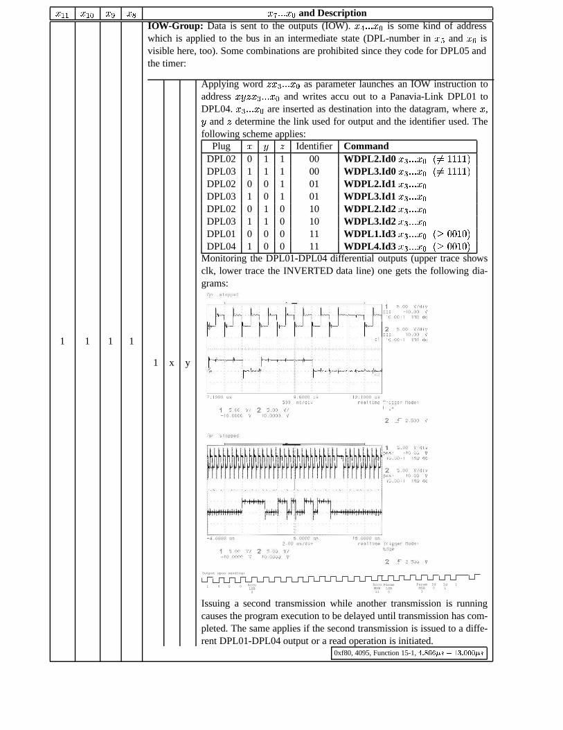
IOW-Group: Data is sent to the outputs (IOW). � 0 � � ��� � is some kind of addresswhich is applied to the bus in an intermediate state (DPL-number in � ; and � � isvisible here, too). Some combinations are prohibited since they code for DPL05 andthe timer:
1 x y
Applying word � � 7 � � ��� � as parameter launches an IOW instruction toaddress � � � � 7 � � ���8� and writes accu out to a Panavia-Link DPL01 toDPL04. � 7 � � ��� � are inserted as destination into the datagram, where � ,� and � determine the link used for output and the identifier used. Thefollowing scheme applies:
Plug � � � Identifier CommandDPL02 0 1 1 00 WDPL2.Id0 � 7 � � ���8� +��� !'!'!'! ,DPL03 1 1 1 00 WDPL3.Id0 � 7 � � ��� � +��� !'!'!'! ,DPL02 0 0 1 01 WDPL2.Id1 � 7 � � ��� �DPL03 1 0 1 01 WDPL3.Id1 � 7 � � ��� �DPL02 0 1 0 10 WDPL2.Id2 � 7 � � ��� �DPL03 1 1 0 10 WDPL3.Id2 � 7 � � ���8�DPL01 0 0 0 11 WDPL1.Id3 � 7 � � ��� � + � �'� ! ��,DPL04 1 0 0 11 WDPL4.Id3 � 7 � � ��� � + � �'� ! ��,
Monitoring the DPL01-DPL04 differential outputs (upper trace showsclk, lower trace the INVERTED data line) one gets the following dia-grams:
Output upon sending:
0 0 0 AccuLSB0
AccuMSB11
ParamLSB0
ParamMSB3
Id0
Id1
11
Issuing a second transmission while another transmission is runningcauses the program execution to be delayed until transmission has com-pleted. The same applies if the second transmission is issued to a diffe-rent DPL01-DPL04 output or a read operation is initiated.
0xf80, 4095, Function 15-1, 0 / � ��� 1�3 �
� 7�/ �����21�3
� ��� � ��� � � � � � � � ��� � and Description
1 1 1 1RETFI: Return from Interrupt if � � � � � � � � �"! .
0xfff, 4095, Function 15-1-127, / � . �21�3
Sun-Sparc SS20512MB, Solaris 2.6Hardware-Control
SGI-Indigo2768MB, IRIX 6.5.22
Visualization
HP1661A102-Channel
Logic-Analyzer
Transputer T805-254MB, Helios,
Homebuilt IO 32bit
BBK-S4Interface
Deviceunder Test:
Programmer ElectronicControlSerial#42
Supplies: 5V (8A), +/-12V (1A), Vcore (1A)
sbus
SPARC
20MBit/sTransputer
Link
Ethernet10MBit/s
GPIB
24 Open-CollectorInput/Outputs andseperate RESET
>64 Channels watching nearlyall vital lines
Setup for analyzing
Programmer Electronic Control
2005 by Erik Baigar,Richard-Strauss-Str. 987616 Marktoberdorf
5 -> Z2/7404 -> 6
9 -> Z2/7404 -> 8
3 -> Z2/7404 -> 4
11 -> Z2/7404 -> 10
Z27 ->4
Z23 ->9
Z17 ->9
6 -> Z25 ->9
Z23 ->4
Z22 ->4
Z17 ->4
13->Z14->10
3 -> Z1/7404 -> 4
9 -> Z1/7404 -> 8
5 -> Z2/7404 -> 640 41
20
18
17
55
54
53
43
Z11/74001112
13
Z7/7438
Z7/7438
60
32
89
10
64
5
OpenCollector
Z7/7438 25
OpenCollector
Z7/7438 45
OpenCollector
42
Z9, &
8
Tornado Computer UnitProgrammer Electronic Control
Control Board, SK7Analyzed 9.11.2005, EBCore Memory Timing
In dieser Spaltesind die Analogen
Chips 55107
To SK1/53DriverBRD
To SK6/53DriverBRD
SK1+SK6/17DriverBRD
SK1+SK6/18DriverBRD
SK1+SK6/19DriverBRD
SK1+SK6/54DriverBRD
59GND SK1+SK6/58DriverBRD
SK2+SK5/43DataBRD
SK2+SK5/42DataBRD
8
10
Z5/7400
Z10/7410NAND, 3in
SK2+SK5/8DataBRD
SK2+SK5/10DataBRD
SK2+SK5/45DataBRD
48GND SK1+SK6/48DriverBRD
Not Driver-or DataBRD
GND
NC?
POD5/77XP
POD5/87YP1
POD5/97ALS
POD5/47XN
POD5/57YN
POD5/67YP
Drive X pos
Drive Y(SK1) pos
Rising Edge:Latch Adress
for line drivers
Drive X neg
Drive Y neg
Drive Y(SK6) pos
POD5/127INH
POD5/27MEMRD
POD5/107MEMOE
Drive inhibitcurrent
Falling edgetriggers Memory
activita: 7MEMRD only is read, together with
leads to write
Low: Send Dataregister to bus
POD5/137NRDS
POD5/157NSELAS
POD5/147NLADA
Low-Pulse readsAmplifier-Signalsinto data latch
High: Data readlatch is set (before
read operation)
Low pulse readsdata from bus intodata latch (for write operation)
Z7/7438 24 POD5/37MEMCK
Memory-Clock outrising edge tellsthat data is vaild
in read cycle
POD5/07NC
No connection and activity
found
65
POD5/17MEMWR
Together with 7MEMRDtriggers write cyclewith falling edge
Z16,&
1
2
4 -> Z21 -> 6,9:NC
Z22 ->6+9
44
POD5/117NRESET
Low duringnormal operationunknown
who drivesthis!
Z5
Z5
Z9
5 4
11
6
9
8
Z9
54
Lots of chips:Z16/4, Z12/4, Z11/4Z10/1, Z5/13, Z1/13
Z1
Z1
6
13
1211
10
Z9
Z9
Z9Z16
12
4
564
PATCH185DPL07-18
PATCH134DPL07-31
PATCH203DPL07-27
PATCH139DPL07-28

SK2
+ S
K5
from SK7
SK1 + SK6
SK1 + SK6
SK3 + SK4

10DataAdr12Bit
Addierer12Bit, 74157Z13,Z19,Z31
Memory12Bit, 2*74174
Z3,Z9
Memory12Bit, 2*74174
Z33,Z35
MUX12 Bit, 2*74157
AND-Gate3*7408
OC-NAND-Driver3*7438
OC-NAND-Driver3*7438
OC-NAND-Driver3*7438
59,24,58,23,57,22,56,21,55,20,54,19
69,33,68,32,67,31,66,30,65,29,64,28
10AUX-Out12Bit
46,9,45,8,44,7,
43,10,42,11,41,12
10AUX-In12Bit
OC-NAND-Driver3*7438
10CYin1410TrEn
49
10MUXSEL48
10ADEN1
10AOEN1
63
27
10ADEN2
10AOEN2
62
26
AND, 0-77430/2
Are Bit0-7High?
51
10LBHI
Tornado Computer UnitProgrammer Electronic Control
Control Register, SK10Analyzed 29.3.2005, EBAdress-Generation (PC)
Globaler Daten- undAdressbus, u.a. zuden Datenboards desCoreMemory: SK2, SK5
AUX-Bus von denbeiden Daten-Registern (X,Y)
SK8 und SK9
AUX-Bus zu denbeiden Daten-Registern (X,Y)
SK8, SK9
10AD0 SK10/59 P1/0 Patch-75 DPL07-510AD1 SK10/24 P1/1 Patch-100 DPL07-610AD2 SK10/58 P1/2 Patch-76 DPL07-710AD3 SK10/23 P1/3 Patch-73 DPL07-810AD4 SK10/57 P1/4 Patch-95 DPL07-910AD5 SK10/22 P1/5 Patch-72 DPL07-10
10AD6 SK10/56 P1/6 Patch-77 DPL07-1110AD7 SK10/21 P1/7 Patch-74 DPL07-1210AD8 SK10/55 P1/8 Patch-94 DPL07-1310AD9 SK10/20 P1/9 Patch-71 DPL07-1410AD10 SK10/54 P1/10 Patch-93 DPL07-15 10AD11 SK10/19 P1/11 Patch-70 DPL07-16 14AD12 SK1/14 ----- Patch162 DPL07-17
10ADEN1 SK10/63 P1/12 10ADEN2 SK10/62 P1/13 10AOEN1 SK10/27 P1/14 Patch-62 DPL07-5110AOEN2 SK10/26 P1/15 Patch-63 DPL07-52
10TrEn SK10/49 P2/010MUXSELSK10/48 P2/110CYin SK10/14 P2/210LBHI SK10/51 P2/310IDXT SK10/13 P2/410MEMEN SK10/53 P2/510PCT SK10/18 P2/610A12 SK10/ 2 P2/710R2 SK10/37 P2/810R3 SK10/ 1 P2/9RESET SK12/ 4 P2/1010FF2I SK10/34 P2/1110FF3I SK10/70 P2/1210FF1I1 SK10/17 P2/1310FF1I2 SK10/16 P2/1410FF1I3 SK10/52 P2/15
12
12
[0-7]
12
12
1212
12 12
12
12
NAND,Z27,7400/2
NAND,Z27,7400/2
T
T
18
13
5310MEMEN
10PCT
10IDXT
Z29,unknown
1
37
2
10R3
10A12
10R2
RR
Reset
7474/2,Z21AFlipFlop
7474/2, Z21BFlipFlop
7474/2, Z15BFlipFlop
OC-NAND-Driver7438
2 37 1
Siehe obenlinks
R R R
3410FF2I
D
10ADEN2 62
70
10FF3I
D
7400/2NAND, Z27
7400/2NAND, Z27
D
171652
10FF1I110FF1I210FF1I3
10MUXSEL
10CYin
10MUXSEL
5410/2, Z253-Fach-NAND
5410/2, Z253-Fach-NAND
10PCT
10MEMEN
TTaktalle drei
FlipFlopsparallel
Minor change, 27.5.06

Tornado Computer Unit,Programmer Electronic Control,
SK13, Rx-Tx-InterfaceAnalyzed by Erik Baigar
22.2.2005
DPL01
DPL02
DPL03
DPL04
55183Output-Driver100Ohm, 2mal
55183Output-Driver100Ohm, 2mal
55183Output-Driver100Ohm, 2mal
18
Clk, approx 2MHz,
50:50
53
Strobe,every 16ms
55183Output-Driver100Ohm, 2mal
33
34
68
69
55182100R-Receiver2 diff. lines
55182100R-Receiver2 diff. lines
55182100R-Receiver2 diff. lines
55182100R-Receiver2 diff. lines
74153 MUX4-to-1Teil1
55182100R-Receiver2 diff. lines
55182100R-Receiver2 diff. lines
55183Output-Driver100Ohm, 2mal
55183Output-Driver100Ohm, 2mal
13ST
13CLK13IRQ1
13IRQ2
13IRQ3
13IRQ4
74153 MUX4-to-1Teil2
19
20
13IN1
13IN2
MUX 1-to-454155Part1
MUX 1-to-454155Part1
13EN16
FreigabeMUXer
51 13O1
13O252
17 5013A 13B
Select-Lines Aand B for allMUXes connected
13EN13IN113IN2
13IRQ113IRQ213IRQ313IRQ4
13A13B
SK13/19SK13/20SK13/16
P5/0P5/1P5/2
P5/3P5/4P5/5P5/6
SK13/17SK13/50
P5/7P5/8
13CLK13ST13O113O2
SK13/18SK13/53SK13/51SK13/52
P5/9P5/10P5/11P5/12
SK13/34SK13/33SK13/68SK13/69
13A SK13/17 POD6/1313B SK13/50 POD6/1213EN SK13/16 POD6/1413CLK SK13/18 POD6/15
Geplante Verkabelung,NICHT UMGESETZT
AKTUELLE VERKABELUNG
1. Update 27.5.20062. Update 11.4.2009
A B
C
R
P
U
L F
K G
M E
D
S T
N
HJ
a
Z V
XY W
b
c
A: CLK Out + B: CLK Out -
C: Data Out +D: Data Out -
E: Data In + F: Data In -
G: CLK In + H: CLK In -
DPL01 - DPL04
V: IRQ out +W: IRQ out -
T: IRQ in + U: IRQ in -
Output upon sending:
Output due to reading:
0 0 0 AccuLSB0
AccuMSB11
ParamLSB0
ParamMSB3
Id0
Id1
1Fix
1 ParamLSB0
ParamMSB3
Id0
Id1
0Fix
1
1
DANGER: Upon reading, PEC sends the headerbut only if the incoming CLK is low. Aftertransmission of the header PEC expects an
incoming transmission of 12 bits terminated byclk-high phase of 2 cycles before it continues.
But maximum waiting time is around 30us!

Counter12Bit, 7493/1*3
Z40,Z37,Z48
Comparator <,>,=12Bit, 7485/1*3Z54, Z55,Z56
Buffer12Bit, 74174*2
Z46,Z47
DPL1-4Sender 16Bit + 4 Bit
16Bit, 74165*2Z38,Z39
DPL5 (Slow Link)Empfaenger/Sender
24Bit, 7495*6Z28-Z32,Z20MUX 4-fach
12Bit, 6*54153Z21-Z24,Z15,Z16
DPL1-4 Empfaenger16Bit, 74164*2
Z11,Z19
Mux0
Mux1
Mux2,Mux3
20
Data-In
13
23
28 Data-Out
Data-In
S/L
T
Internal buffered 12-Bit-IO-Bus
INVZ4
T
22
Output-Drivers12Bit, 7438/1*3
Z13,Z14,Z8
Input-Buffer12Bit, 7400/2*3
Z5-Z7
IO-Bus:D0-61 D6-62D1-60 D7-63D2-59 D8-55D3-58 D9-54D4-57 D10-53D5-56 D11-52
A B
NANDZ26
NANDZ26
11
5
6
1,1435,50
INVZ8
CD401068, Z2
TR
Data-In??
Tornado Computer Unit,Programmer Electronic Control,SK14, Serial Parallel Converter
Analyzed by Erik Baigar21.4.2005
14IOR
14IOW
14DIN1
14DIN0
14T0
14SL0
14DOUT0
14TR2
14TIME
14MUXA 14MUXB
14MUX
AD0-12
14IOW14IOR14DIN114MUXA14MUXB14MUX14DIN014T014SL014DOUT014TR214TIME
SK14/6SK14/5SK14/20SK14/11SK14/10SK14/12SK14/13SK14/18SK14/23SK14/28SK14/1SK14/22
POD6/0POD6/1POD6/2POD6/3POD6/4POD6/5POD6/6POD6/7POD6/8POD6/9POD6/10POD6/11
12
10
181. Update 27.5.20062. Update 10.4.2009
1,2
A<B
Z4504/2
Z63, 7432,3-NAND
9 14TIRQ
Z17, 5432T
19 14CLKIN


![ADDP-ME-ED0003571 · Web viewADDP-ME-ED0003571 Rev. [-] Page 13 of 16 ADDP-ME-ED0003571 Rev. [-] Page 12 of 16 Accelerator Division Mechanical Support Department CONTROLLED DOCUMENT](https://static.fdocuments.in/doc/165x107/60bffb1ccd1b21075f41bfc8/addp-me-ed0003571-web-view-addp-me-ed0003571-rev-page-13-of-16-addp-me-ed0003571.jpg)