
Programmable LED Driver - Farnell element14 · Unless otherwise noted, specifications apply to...
18
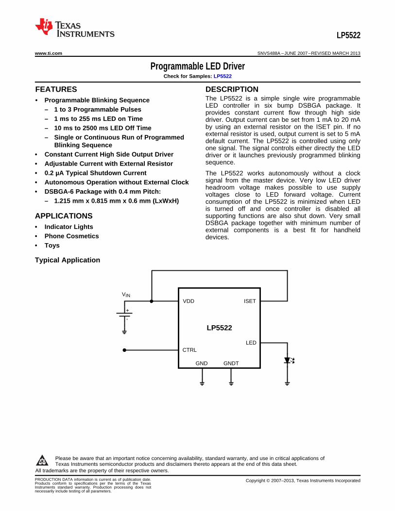
LP5522 - + GND GNDT CTRL VDD ISET LED V IN LP5522 www.ti.com SNVS488A – JUNE 2007 – REVISED MARCH 2013 Programmable LED Driver Check for Samples: LP5522 1FEATURES DESCRIPTION The LP5522 is a simple single wire programmable 2• Programmable Blinking Sequence LED controller in six bump DSBGA package. It – 1 to 3 Programmable Pulses provides constant current flow through high side – 1 ms to 255 ms LED on Time driver. Output current can be set from 1 mA to 20 mA by using an external resistor on the ISET pin. If no – 10 ms to 2500 ms LED Off Time external resistor is used, output current is set to 5 mA – Single or Continuous Run of Programmed default current. The LP5522 is controlled using only Blinking Sequence one signal. The signal controls either directly the LED • Constant Current High Side Output Driver driver or it launches previously programmed blinking sequence. • Adjustable Current with External Resistor • 0.2 μA Typical Shutdown Current The LP5522 works autonomously without a clock signal from the master device. Very low LED driver • Autonomous Operation without External Clock headroom voltage makes possible to use supply • DSBGA-6 Package with 0.4 mm Pitch: voltages close to LED forward voltage. Current – 1.215 mm x 0.815 mm x 0.6 mm (LxWxH) consumption of the LP5522 is minimized when LED is turned off and once controller is disabled all supporting functions are also shut down. Very small APPLICATIONS DSBGA package together with minimum number of • Indicator Lights external components is a best fit for handheld • Phone Cosmetics devices. • Toys Typical Application 1 Please be aware that an important notice concerning availability, standard warranty, and use in critical applications of Texas Instruments semiconductor products and disclaimers thereto appears at the end of this data sheet. 2All trademarks are the property of their respective owners. PRODUCTION DATA information is current as of publication date. Copyright © 2007–2013, Texas Instruments Incorporated Products conform to specifications per the terms of the Texas Instruments standard warranty. Production processing does not necessarily include testing of all parameters.
Transcript of Programmable LED Driver - Farnell element14 · Unless otherwise noted, specifications apply to...
LP5522
-+
GND GNDT
CTRL
VDD ISET
LED
VIN
LP5522
www.ti.com SNVS488A –JUNE 2007–REVISED MARCH 2013
Programmable LED DriverCheck for Samples: LP5522
1FEATURES DESCRIPTIONThe LP5522 is a simple single wire programmable
2• Programmable Blinking SequenceLED controller in six bump DSBGA package. It
– 1 to 3 Programmable Pulses provides constant current flow through high side– 1 ms to 255 ms LED on Time driver. Output current can be set from 1 mA to 20 mA
by using an external resistor on the ISET pin. If no– 10 ms to 2500 ms LED Off Timeexternal resistor is used, output current is set to 5 mA– Single or Continuous Run of Programmed default current. The LP5522 is controlled using only
Blinking Sequence one signal. The signal controls either directly the LED• Constant Current High Side Output Driver driver or it launches previously programmed blinking
sequence.• Adjustable Current with External Resistor• 0.2 µA Typical Shutdown Current The LP5522 works autonomously without a clock
signal from the master device. Very low LED driver• Autonomous Operation without External Clockheadroom voltage makes possible to use supply
• DSBGA-6 Package with 0.4 mm Pitch: voltages close to LED forward voltage. Current– 1.215 mm x 0.815 mm x 0.6 mm (LxWxH) consumption of the LP5522 is minimized when LED
is turned off and once controller is disabled allsupporting functions are also shut down. Very smallAPPLICATIONSDSBGA package together with minimum number of
• Indicator Lights external components is a best fit for handheld• Phone Cosmetics devices.• Toys
Typical Application
1
Please be aware that an important notice concerning availability, standard warranty, and use in critical applications ofTexas Instruments semiconductor products and disclaimers thereto appears at the end of this data sheet.
2All trademarks are the property of their respective owners.
PRODUCTION DATA information is current as of publication date. Copyright © 2007–2013, Texas Instruments IncorporatedProducts conform to specifications per the terms of the TexasInstruments standard warranty. Production processing does notnecessarily include testing of all parameters.

LED GND GNDT
CTRLVDD ISET
A B C
2
1
LEDGNDGNDT
CTRL VDDISET
ABC
2
1
LP5522
SNVS488A –JUNE 2007–REVISED MARCH 2013 www.ti.com
Connection Diagrams
DSBGA-6 package, 0.815 x 1.215 x 0.60 mm body size, 0.4 mm pitch, Package Number YFQ0006
Figure 1. Top View Figure 2. Bottom View
PIN DESCRIPTIONS (1)
Pin Name Type Description
A1 VDD P Power supply pin
B1 ISET AI Current set input
C1 CTRL DI Digital control input
A2 LED AO Current source output
B2 GND G Ground
C2 GNDT G Ground
(1) A: Analog Pin, D: Digital Pin, G: Ground Pin, P: Power Pin, I: Input Pin, O: Output Pin
These devices have limited built-in ESD protection. The leads should be shorted together or the device placed in conductive foamduring storage or handling to prevent electrostatic damage to the MOS gates.
Absolute Maximum Ratings (1) (2) (3)
V (VDD, LED, ISET) -0.3V to +6.0V
Voltage on logic pin (CTRL) -0.3V to VDD +0.3Vwith 6.0V max
Continuous Power Dissipation (4) Internally Limited
Junction Temperature (TJ-MAX) 125°C
Storage Temperature Range -65°C to +150°C
Maximum Lead Temperature (Reflow soldering, 3 times) 260°C(5)
ESD Rating (6)
Human Body Model 2 kV
(1) Absolute Maximum Ratings indicate limits beyond which damage to the component may occur. Operating Ratings are conditions underwhich operation of the device is ensured. Operating Ratings do not imply ensured performance limits. For ensured performance limitsand associated test conditions, see the Electrical Characteristics tables.
(2) All voltages are with respect to the potential at the GND pins.(3) If Military/Aerospace specified devices are required, please contact the Texas Instruments Office/ Distributors for availability and
specifications.(4) Internal thermal shutdown circuitry protects the device from permanent damage. Thermal shutdown engages at TJ=160°C (typ.) and
disengages at TJ=140°C (typ.).(5) For detailed soldering specifications and information, please refer to Application Note AN1112 : DSBGA Wafer Level Chip Scale
Package SNVA009.(6) The Human body model is a 100 pF capacitor discharged through a 1.5 kΩ resistor into each pin. MIL-STD-883 3015.7
2 Submit Documentation Feedback Copyright © 2007–2013, Texas Instruments Incorporated
Product Folder Links: LP5522

LP5522
www.ti.com SNVS488A –JUNE 2007–REVISED MARCH 2013
Operating Ratings (1) (2)
Voltage on power pin (VDD) 2.7V to 5.5V
Recommended Load Current 1 mA to 20 mA
Junction Temperature (TJ) Range -30°C to +125°C
Ambient Temperature (TA) Range (3) -30°C to +85°C
(1) Absolute Maximum Ratings indicate limits beyond which damage to the component may occur. Operating Ratings are conditions underwhich operation of the device is ensured. Operating Ratings do not imply ensured performance limits. For ensured performance limitsand associated test conditions, see the Electrical Characteristics tables.
(2) All voltages are with respect to the potential at the GND pins.(3) In applications where high power dissipation and/or poor package thermal resistance is present, the maximum ambient temperature may
have to be derated. Maximum ambient temperature (TA-MAX) is dependent on the maximum operating junction temperature (TJ-MAX-OP =125°C), the maximum power dissipation of the device in the application (PD-MAX), and the junction-to ambient thermal resistance of thepart/package in the application (θJA), as given by the following equation: TA-MAX = TJ-MAX-OP – (θJA × PD-MAX).
Thermal PropertiesJunction-to-Ambient Thermal Resistance (θJA) (1) 87°C/W
(1) Junction-to-ambient thermal resistance is highly application and board-layout dependent. In applications where high maximum powerdissipation exists, special care must be paid to thermal dissipation issues in board design.
Copyright © 2007–2013, Texas Instruments Incorporated Submit Documentation Feedback 3
Product Folder Links: LP5522

LP5522
SNVS488A –JUNE 2007–REVISED MARCH 2013 www.ti.com
Electrical Characteristics (1) (2)
Limits in standard typeface are for TJ = 25°C. Limits in boldface type apply over the operating ambient temperature range (-30°C < TA < +85°C). Unless otherwise noted, specifications apply to LP5522 Block Diagram with: VIN = 3.6V, RISET = 24 kΩ,CIN = 100 nF.
Symbol Parameter Condition Min Typ Max Units
IVDD Standby supply current CTRL = L 0.2 1 µA
Active Mode Supply Current CTRL = H, LED = off 40 55 µA
ILEAKAGE LED Pin Leakage Current 1 µA
IOUT LED Output Current Without external resistor 5 mA−8 +8 %
LED Output Current With external 24kΩ 0.04% resistor 20 mA−8 +8 %
IMIRROR External RISET 1:400Mirroring Ratio
VISET ISET Reference Voltage 1.23 V
VHR Minimum Headroom Voltage IOUT set to 10 mA 35 50 mV(VIN - VLED) (3)
IOUT set to 20 mA 70 100 mV
T_CYCLE_H Minimum LED On Time 0.9 1.0 1.1 ms
T_CYCLE_L Minimum LED Off Time 9 10 11 ms
ONRESOLUTION LED On Time Resolution 1 ms
OFFRESOLUTIO LED Off Time Resolution 10 msN
T_Timeout_H LED Timeout On Time 287 319 351 ms
T_Timeout_L LED Timeout Off Time 2.87 3.19 3.51 s
VIL Logic Input Low Level 0.5 V
VIH Logic Input High Level 1.2 V
IIN CTRL Input Current -1 1 µA
tON CTRL Pulse ON Time 15 µs
tOFF CTRL Pulse OFF Time 30 µs
tENTER Command Entering Period 500 µs
tENTER+tBLANK Command Entering Period + 1500 µsBlank Period
(1) All voltages are with respect to the potential at the GND pins.(2) Min and Max limits are ensured by design, test, or statistical analysis. Typical numbers are not ensured, but do represent the most likely
norm.(3) The current source is connected internally between VIN an VLED. The voltage across the current source, (VIN - VLED), is referred to a
headroom voltage (VHR). Minimum headroom voltage is defined as the VHR voltage when the LED current has dropped 10% from thevalue measured at VLED = VIN - 1V.
4 Submit Documentation Feedback Copyright © 2007–2013, Texas Instruments Incorporated
Product Folder Links: LP5522

LP5522
www.ti.com SNVS488A –JUNE 2007–REVISED MARCH 2013
LP5522 BLOCK DIAGRAM
Copyright © 2007–2013, Texas Instruments Incorporated Submit Documentation Feedback 5
Product Folder Links: LP5522

RESET
STANDBY
ACTIVE
POR = L
Control command
POR
Control commandends
POR = H
LP5522
SNVS488A –JUNE 2007–REVISED MARCH 2013 www.ti.com
Modes of Operation
RESET In the reset mode all functions are off and all registers are reset to the default values. Reset is enteredalways if internal Power On Reset (POR) is active. Power On Reset will activate during the device startupor when the supply voltage VIN falls below 1.5V (typ.).
STANDBY: After Power On Reset device is in Standby mode. This is the low power consumption mode, whenall circuit functions are disabled.
ACTIVE: Once rising edge of CTRL signal is detected device goes into Active mode. In Active mode four submodes are present:
RUN: Run mode is divided into two sub modes depending on whether a blinking sequence is programmed intomemory or not.
Non-programmed mode:No blinking sequence programmed to memory. LED output follows CTRL input
Programmed mode:Blinking sequence programmed to memory. LED output follows the programmed blinkingsequence
RUN ONCE: In Run once mode, programmed blinking sequence is performed once and after that devicereturns into Standby mode. Run once mode is available only if a blinking sequence is programmed intomemory.
TRAINING: In Training mode new blinking sequence can be programmed. LED output follows CTRL signalduring the programming
TSD: If chip temperature rises above 160°C (typ.) device goes into Thermal Shut Down (TSD) mode. In TSDmode output is disabled but supporting functions are on.
LED Driver Operational Description
The LP5522 LED driver is constant current source. Current can be set with external resistor (RISET) so that thecurrent ratio between resistor and LED is 1:400. RISET current correlates to ISET reference voltage (VISET).Consequently, current through LED can be adjusted using equation IOUT = 480/RISET.
Use of external resistor is optional. If external resistor is not connected, default output current is 5 mA. Whenexternal resistor is not used ISET pin should be connected to VDD.
6 Submit Documentation Feedback Copyright © 2007–2013, Texas Instruments Incorporated
Product Folder Links: LP5522

LP5522
www.ti.com SNVS488A –JUNE 2007–REVISED MARCH 2013
LED Driver Typical Performance CharacteristicsTJ = 25°C. Unless otherwise noted, typical performance characteristics apply to LP5522 Block Diagram with: VIN = 3.6V, RISET
= 24 kΩ, CIN = 100 nF.
Output Current vs RISET (Expanded Range) Output Current vs RISET
Figure 3. Figure 4.
Output Current vs Input Voltage(ISET Connected To VDD) Output Current vs Headroom Voltage
Figure 5. Figure 6.
Line Regulation LED Startup
Figure 7. Figure 8.
Copyright © 2007–2013, Texas Instruments Incorporated Submit Documentation Feedback 7
Product Folder Links: LP5522

Command entering period Blank period Command execution starts
CTRL
LED
Command entering period Blank period Command execution starts
CTRL
LED
LP5522
SNVS488A –JUNE 2007–REVISED MARCH 2013 www.ti.com
CONTROL INTERFACE OPERATIONAL DESCRIPTION
LP5522 has one digital control input, CTRL. Threshold levels of CTRL input are fixed to enable control from lowvoltage controller. CTRL signal is used to control the mode of the circuit. A rising edge of the CTRL signalactivates the circuit and starts a command entering period. During the command entering period all rising edgesare counted. After command entering period there is a blank period when no rising edges are allowed. If CTRL isleft high after command entering period, the consequent command is performed right after the blank period.
Note that timing diagrams are not on scale!
If CTRL signal is low after command entering period, command execution starts when CTRL is pulled high. Thisdoes not apply to Run command. With Run command CTRL must be high. Note that no rising edges are allowedduring blank period.
LED Controller Commands and Operation
There are four commands available for LP5522.
Command Number of rising edges during command entering period
Run One rising edge
Training start Two rising edges
Training end Three rising edges
Run once Four rising edges
RUN COMMAND
One rising edge of CTRL signal within command entering period is interpreted as Run command. In programmedmode blinking sequence is started right after Blank period and it is repeated as long as CTRL signal is kept high.When CTRL signal is set low device goes into Standby mode.
8 Submit Documentation Feedback Copyright © 2007–2013, Texas Instruments Incorporated
Product Folder Links: LP5522

Command entering period
Blank period
CTRL
LED
To Standby
Programmed sequence
Command entering period
Blank period
CTRL
LED
To Standby
Programmed sequence
Command entering period
Blank period
CTRL
LED
To Standby
Command entering period
Blank period Programmed sequence
CTRL
LED
To Standby
LP5522
www.ti.com SNVS488A –JUNE 2007–REVISED MARCH 2013
In non-programmed mode LED is on as long as CTRL is kept high. When CTRL signal is set low device goesinto Standby mode.
RUN ONCE COMMAND
Programmed blinking sequence is performed once after Run Once command. Four rising edges of CTRL signalwithin command entering period is interpreted as Run Once command. If CTRL is kept high after commandentering period the programmed blinking sequence starts right after the blank period has elapsed. CTRL signalmust stay high as long as programmed blinking sequence is executed. If CTRL is set low during execution ofblinking sequence, device goes to standby and execution of blinking sequence is stopped.
If CTRL signal is low after command entering period, Run Once command is executed once the CTRL is sethigh.
Copyright © 2007–2013, Texas Instruments Incorporated Submit Documentation Feedback 9
Product Folder Links: LP5522

1st ON time 1st OFF time
CTRL
LED
2nd ONtime
2nd OFF time tENTER
To Standby
Blank period
Command entering period
Blank period
CTRL
LED
1st ON Time 1st OFF Timestarts
LP5522
SNVS488A –JUNE 2007–REVISED MARCH 2013 www.ti.com
TRAINING START COMMAND
Blinking sequence is programmed into memory in training mode. Blinking sequence is stored into volatilememory, thus removing input voltage VIN resets the memory. Memory can also be reset by giving Training Startand Training End commands without any valid LED ON/OFF times.
LP5522 enters to Training mode after Training Start command. Two rising edges within command enteringperiod is interpreted as the Training Start command. The first LED ON time capturing is started once the risingedge of CTRL signal is detected after the blank period. LED output follows CTRL signal during the programming.
The first LED ON time is recorded once CTRL signal is set low. Same time the first LED OFF time capturing isstarted. Programmed blinking sequence can have one to three LED ON/OFF times. In order to be programmedcorrectly, at least one valid LED ON and LED OFF time must be recorded.
TRAINING END COMMAND
Blinking sequence programming ends once Training End command is introduced. Three rising edges within timeperiod of tENTER is interpreted as Training End command. Note that blank period is also reguired after TrainingEnd command. During blanc period no rising edges are allowed.
When Training End command is introduced during LED OFF time capturing, LED OFF time is recorded and chipgoes to standby mode.
If Training End command is introduced during LED ON time capturing, the associated LED ON period is notrecorded and hence neither OFF time. Notice that valid OFF time before Training End is longer than half ofMinimum LED OFF period (T_CYCLE_L).
10 Submit Documentation Feedback Copyright © 2007–2013, Texas Instruments Incorporated
Product Folder Links: LP5522

tENTER + tBLANK
CTRL
LED
To Standby
T_TIMEOUT_L
Run once command To Standby
tENTER + tBLANK
CTRL
LED
To Standby
T_TIMEOUT_H T_TIMEOUT_L
Run command
1st ON time 1st OFF time
CTRL
LED
2nd ONtime
t < ½*T_CYCLE_L
tENTER
To Standby
Blank period
LP5522
www.ti.com SNVS488A –JUNE 2007–REVISED MARCH 2013
LED TIMEOUT ON/OFF TIMES
When LP5522 is in training mode and CTRL signal is high longer than LED Timeout ON time, the ON timecounter saturates. In this case saturated ON time is recorded and LED OFF time capturing is started. At thesame time LED is switched off even if the CTRL signal is still high.
If ON time counter has saturated, LED OFF time recording is terminated either by giving a Train End commandor setting the CTRL signal to low and back to high. Setting the CTRL signal back to high records the LED OFFtime and starts next ON time capturing.
If anyhow CTRL is still high after the LED Timeout OFF time has been elapsed the OFF time counter saturatesand saturated OFF time is recorded. After that chip waits the CTRL signal to go low which cause the chip to goStandby.
LED OFF time counter can saturate also if Training end command is not given or no new ON time has beenstarted. In this case saturated OFF time is recorded and chip goes to Standby.
Copyright © 2007–2013, Texas Instruments Incorporated Submit Documentation Feedback 11
Product Folder Links: LP5522

LP5522
SNVS488A –JUNE 2007–REVISED MARCH 2013 www.ti.com
Recommended External Components
INPUT CAPACITOR, CIN
Although not required for normal operation, a capacitor can be added to VIN to reduce line noise. A surface-mount multi-layer ceramic capacitor (MLCC) is recommended. MLCCs with a X7R or X5R temperaturecharacteristic are preferred.
CURRENT SET RESISTOR, RISET
If other than 5 mA current is required, RISET resistor can be used to adjust the current. For 20 mA current 24 kΩresistor is required. Accuracy of the resistor directly effects to the accuracy of the LED current. 1% or better isrecommended.
LED
Forward voltage of LED must be less than minimum input voltage minus minimum headroom voltage (VHR). Forexample with 2.7V input voltage and 20 mA LED current the maximum LED forward voltage is 2.7V - 100 mV =2.6V.
List of Recommended External Components
Symbol Symbol Explanation Value Unit Type
CIN VDD Bypass Capacitor 100 nF Ceramic, X7R or X5R
RISET Current Set Resistor for 20 mA LED Current 24 kΩ 1%
LED User defined
12 Submit Documentation Feedback Copyright © 2007–2013, Texas Instruments Incorporated
Product Folder Links: LP5522

LP5522
www.ti.com SNVS488A –JUNE 2007–REVISED MARCH 2013
REVISION HISTORY
Changes from Original (March 2013) to Revision A Page
• Changed layout of National Data Sheet to TI format .......................................................................................................... 12
Copyright © 2007–2013, Texas Instruments Incorporated Submit Documentation Feedback 13
Product Folder Links: LP5522

PACKAGE OPTION ADDENDUM
www.ti.com 11-Apr-2013
Addendum-Page 1
PACKAGING INFORMATION
Orderable Device Status(1)
Package Type PackageDrawing
Pins PackageQty
Eco Plan(2)
Lead/Ball Finish MSL Peak Temp(3)
Op Temp (°C) Top-Side Markings(4)
Samples
LP5522TM/NOPB ACTIVE DSBGA YFQ 6 250 Green (RoHS& no Sb/Br)
SNAGCU Level-1-260C-UNLIM -30 to 85 6
LP5522TMX/NOPB ACTIVE DSBGA YFQ 6 3000 Green (RoHS& no Sb/Br)
SNAGCU Level-1-260C-UNLIM -30 to 85 6
(1) The marketing status values are defined as follows:ACTIVE: Product device recommended for new designs.LIFEBUY: TI has announced that the device will be discontinued, and a lifetime-buy period is in effect.NRND: Not recommended for new designs. Device is in production to support existing customers, but TI does not recommend using this part in a new design.PREVIEW: Device has been announced but is not in production. Samples may or may not be available.OBSOLETE: TI has discontinued the production of the device.
(2) Eco Plan - The planned eco-friendly classification: Pb-Free (RoHS), Pb-Free (RoHS Exempt), or Green (RoHS & no Sb/Br) - please check http://www.ti.com/productcontent for the latest availabilityinformation and additional product content details.TBD: The Pb-Free/Green conversion plan has not been defined.Pb-Free (RoHS): TI's terms "Lead-Free" or "Pb-Free" mean semiconductor products that are compatible with the current RoHS requirements for all 6 substances, including the requirement thatlead not exceed 0.1% by weight in homogeneous materials. Where designed to be soldered at high temperatures, TI Pb-Free products are suitable for use in specified lead-free processes.Pb-Free (RoHS Exempt): This component has a RoHS exemption for either 1) lead-based flip-chip solder bumps used between the die and package, or 2) lead-based die adhesive used betweenthe die and leadframe. The component is otherwise considered Pb-Free (RoHS compatible) as defined above.Green (RoHS & no Sb/Br): TI defines "Green" to mean Pb-Free (RoHS compatible), and free of Bromine (Br) and Antimony (Sb) based flame retardants (Br or Sb do not exceed 0.1% by weightin homogeneous material)
(3) MSL, Peak Temp. -- The Moisture Sensitivity Level rating according to the JEDEC industry standard classifications, and peak solder temperature.
(4) Multiple Top-Side Markings will be inside parentheses. Only one Top-Side Marking contained in parentheses and separated by a "~" will appear on a device. If a line is indented then it is acontinuation of the previous line and the two combined represent the entire Top-Side Marking for that device.
Important Information and Disclaimer:The information provided on this page represents TI's knowledge and belief as of the date that it is provided. TI bases its knowledge and belief on informationprovided by third parties, and makes no representation or warranty as to the accuracy of such information. Efforts are underway to better integrate information from third parties. TI has taken andcontinues to take reasonable steps to provide representative and accurate information but may not have conducted destructive testing or chemical analysis on incoming materials and chemicals.TI and TI suppliers consider certain information to be proprietary, and thus CAS numbers and other limited information may not be available for release.
In no event shall TI's liability arising out of such information exceed the total purchase price of the TI part(s) at issue in this document sold by TI to Customer on an annual basis.
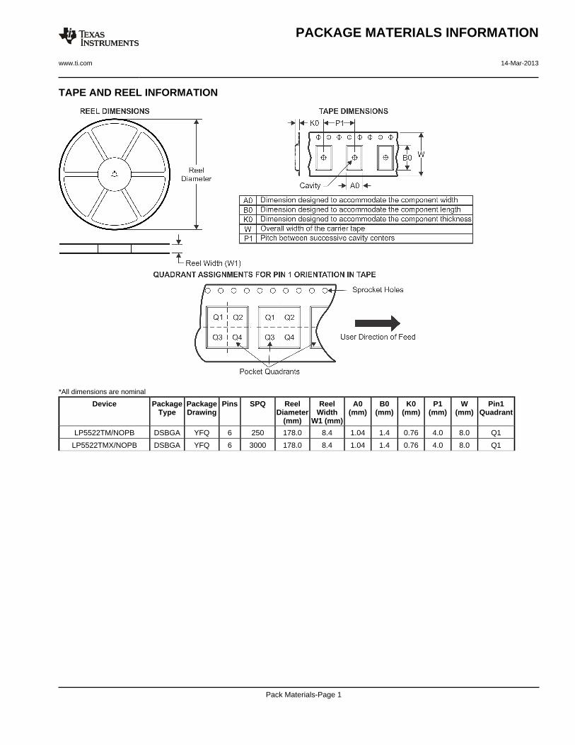
TAPE AND REEL INFORMATION
*All dimensions are nominal
Device PackageType
PackageDrawing
Pins SPQ ReelDiameter
(mm)
ReelWidth
W1 (mm)
A0(mm)
B0(mm)
K0(mm)
P1(mm)
W(mm)
Pin1Quadrant
LP5522TM/NOPB DSBGA YFQ 6 250 178.0 8.4 1.04 1.4 0.76 4.0 8.0 Q1
LP5522TMX/NOPB DSBGA YFQ 6 3000 178.0 8.4 1.04 1.4 0.76 4.0 8.0 Q1
PACKAGE MATERIALS INFORMATION
www.ti.com 14-Mar-2013
Pack Materials-Page 1

*All dimensions are nominal
Device Package Type Package Drawing Pins SPQ Length (mm) Width (mm) Height (mm)
LP5522TM/NOPB DSBGA YFQ 6 250 210.0 185.0 35.0
LP5522TMX/NOPB DSBGA YFQ 6 3000 210.0 185.0 35.0
PACKAGE MATERIALS INFORMATION
www.ti.com 14-Mar-2013
Pack Materials-Page 2

MECHANICAL DATA
YFQ0006xxx
www.ti.com
TMD06XXX (Rev B)
E
0.600±0.075
D
A. All linear dimensions are in millimeters. Dimensioning and tolerancing per ASME Y14.5M-1994.B. This drawing is subject to change without notice.
NOTES:
4215075/A 12/12
D: Max =
E: Max =
1.24 mm, Min =
0.84 mm, Min =
1.18 mm
0.78 mm

IMPORTANT NOTICE
Texas Instruments Incorporated and its subsidiaries (TI) reserve the right to make corrections, enhancements, improvements and otherchanges to its semiconductor products and services per JESD46, latest issue, and to discontinue any product or service per JESD48, latestissue. Buyers should obtain the latest relevant information before placing orders and should verify that such information is current andcomplete. All semiconductor products (also referred to herein as “components”) are sold subject to TI’s terms and conditions of salesupplied at the time of order acknowledgment.
TI warrants performance of its components to the specifications applicable at the time of sale, in accordance with the warranty in TI’s termsand conditions of sale of semiconductor products. Testing and other quality control techniques are used to the extent TI deems necessaryto support this warranty. Except where mandated by applicable law, testing of all parameters of each component is not necessarilyperformed.
TI assumes no liability for applications assistance or the design of Buyers’ products. Buyers are responsible for their products andapplications using TI components. To minimize the risks associated with Buyers’ products and applications, Buyers should provideadequate design and operating safeguards.
TI does not warrant or represent that any license, either express or implied, is granted under any patent right, copyright, mask work right, orother intellectual property right relating to any combination, machine, or process in which TI components or services are used. Informationpublished by TI regarding third-party products or services does not constitute a license to use such products or services or a warranty orendorsement thereof. Use of such information may require a license from a third party under the patents or other intellectual property of thethird party, or a license from TI under the patents or other intellectual property of TI.
Reproduction of significant portions of TI information in TI data books or data sheets is permissible only if reproduction is without alterationand is accompanied by all associated warranties, conditions, limitations, and notices. TI is not responsible or liable for such altereddocumentation. Information of third parties may be subject to additional restrictions.
Resale of TI components or services with statements different from or beyond the parameters stated by TI for that component or servicevoids all express and any implied warranties for the associated TI component or service and is an unfair and deceptive business practice.TI is not responsible or liable for any such statements.
Buyer acknowledges and agrees that it is solely responsible for compliance with all legal, regulatory and safety-related requirementsconcerning its products, and any use of TI components in its applications, notwithstanding any applications-related information or supportthat may be provided by TI. Buyer represents and agrees that it has all the necessary expertise to create and implement safeguards whichanticipate dangerous consequences of failures, monitor failures and their consequences, lessen the likelihood of failures that might causeharm and take appropriate remedial actions. Buyer will fully indemnify TI and its representatives against any damages arising out of the useof any TI components in safety-critical applications.
In some cases, TI components may be promoted specifically to facilitate safety-related applications. With such components, TI’s goal is tohelp enable customers to design and create their own end-product solutions that meet applicable functional safety standards andrequirements. Nonetheless, such components are subject to these terms.
No TI components are authorized for use in FDA Class III (or similar life-critical medical equipment) unless authorized officers of the partieshave executed a special agreement specifically governing such use.
Only those TI components which TI has specifically designated as military grade or “enhanced plastic” are designed and intended for use inmilitary/aerospace applications or environments. Buyer acknowledges and agrees that any military or aerospace use of TI componentswhich have not been so designated is solely at the Buyer's risk, and that Buyer is solely responsible for compliance with all legal andregulatory requirements in connection with such use.
TI has specifically designated certain components as meeting ISO/TS16949 requirements, mainly for automotive use. In any case of use ofnon-designated products, TI will not be responsible for any failure to meet ISO/TS16949.
Products Applications
Audio www.ti.com/audio Automotive and Transportation www.ti.com/automotive
Amplifiers amplifier.ti.com Communications and Telecom www.ti.com/communications
Data Converters dataconverter.ti.com Computers and Peripherals www.ti.com/computers
DLP® Products www.dlp.com Consumer Electronics www.ti.com/consumer-apps
DSP dsp.ti.com Energy and Lighting www.ti.com/energy
Clocks and Timers www.ti.com/clocks Industrial www.ti.com/industrial
Interface interface.ti.com Medical www.ti.com/medical
Logic logic.ti.com Security www.ti.com/security
Power Mgmt power.ti.com Space, Avionics and Defense www.ti.com/space-avionics-defense
Microcontrollers microcontroller.ti.com Video and Imaging www.ti.com/video
RFID www.ti-rfid.com
OMAP Applications Processors www.ti.com/omap TI E2E Community e2e.ti.com
Wireless Connectivity www.ti.com/wirelessconnectivity
Mailing Address: Texas Instruments, Post Office Box 655303, Dallas, Texas 75265Copyright © 2013, Texas Instruments Incorporated