Program & Abstracts - McGill PhysicsSPM/nano2012/cifar_rqmp_nano2012_progra… · Program &...
52
& May , 2012 at McGill University in 21-25 Montreal Nanoelectronics Summer School 2012 Program & Abstracts
Transcript of Program & Abstracts - McGill PhysicsSPM/nano2012/cifar_rqmp_nano2012_progra… · Program &...

&
May , 2012 at McGill University in 21-25 MontrealNanoelectronics Summer School 2012
Program & Abstracts

A
D
F
B B
B C
E
E
A A
A A
AMcConnell Engineering Bldg3480 rue University, room 13
Rutherford Physics Building3600 rue University, board room
Trottier Building3630 rue University, lobby
New Residence Hall3625 avenue du Parc, lobby
Centre Mont-Royal2200 rue Mansfield
Restaurant L'Academie2100 rue Crescent
B
C
D
E
F

INVITED TALKS
Kirk Bevan Department of Mining and Materials Engineering, Department of Physics, McGill University
Using Effective Mass Models in Nanoelectronics
Tuesday 9:00-10:00 am
In this talk the fundamentals, applications, advantages, and limitations of the effective mass
approximation in nanoelectronic device modeling will be covered. Starting from the fundamental
finite difference approach, we will examine the importance band bending, doping, and self-
consistency in capturing device and materials phenomena. An emphasis will be placed on length
scales on the order of 100nm.
Using Atomistic Models in Nanoelectronics
Tuesday 10:30-11:30 am
In this talk the various types of atomistic models will be covered, with an overview of their
benefits and limitations. In particular, we will cover the recent rise in popularity of atomistic
models to capture bulk properties, as well as interface and surface interactions between distinct
materials in nanoelectronic architectures. The state-of-the-art will be overviewed in capturing
various materials and device structures. This will include an overview of magnetoresistance,
semiconductor-oxide interfaces, Schottky junctions, and associated phenomena. An emphasis
will be placed on length scales on the order of 10nm and below.
Some Engineering Challenges in Nanoelectronics
Tuesday 1:00-2:00 pm
In this talk we will cover some of the rising and existing engineering challenges in
nanoelectronic device design and semiconductor scaling. This will include coverage of issues
such as power consumption, leakage currents, interconnect capacitance, and next generation
memory storage. An overall emphasis will be placed on the concepts of reliability and
manufacturing variability in the maturation of any new prototype nanoelectronic technology.

INVITED TALKS
Iain R. McNab School of Biological Sciences and Applied Chemistry,
Seneca College of Applied Arts & Technology
Tuesday 2:30-4:30 pm
The Polanyi laboratory has recently been studying adsorption and reactions of molecules at
surfaces, leading to chemically attached (robust) nano-patterns.
These studies use Scanning Tunneling Microscopy to track adsorption and reaction,
augmented with first-principles calculations. The calculations are needed both to interpret the
STM images and to provide energetics of physisorption and reactive processes at the surface.
I will discuss:
1. the charge distribution at surfaces, with particular reference to the Si(111)-7x7 surface
2. modification of the surface charge distribution by physisorption and chemisorption
3. physisorption patterns of mobile and immobile species, captured by STM, and interpreted
with theory
4. mobile precursors to reaction.
Thomas Szkopek Department of Electrical and Computer Engineering, Department of Physics, McGill University
Wednesday 9:00-10:00 am & 10:30-11:30 am
Graphene - the first and most well known of the new material family of 2D atomic crystals - is
unique in its combination of material properties. In this talk, I will describe the synthesis and
electrical properties of graphene, with an emphasis on new opportunities for graphene
applications. The advent of chemical vapour deposition growth of graphene on Cu enables the
synthesis of continuous monolayer graphene films extending over macroscopic areas. Raman
spectroscopy and electron transport indicate high material quality.
The high-mobility conduction of electrons at a surface in graphene translates into the
facile measurement of surface potential. Examples of charge detection include the real-time
monitoring of surface redox reactions with atto-ampere current sensitivity, and ion trapping / de-
trapping at Si/SiO2 interfaces. Non-covalent functionalization can be used to enhance the
adsorbate sensitivity of graphene field effect transistors, including small gas molecules.
The high mobility of graphene is attractive for high-frequency applications, including
high-speed transistors, frequency multipliers and non-reciprocal devices such as Faraday
rotators. Microwave frequency transport measurements to 110GHz of graphene reveal the
complete absence of skin-effects and anomalous magneto-resistance.
My talk concludes with a discussion of the current state of the art in 2D atomic crystal
synthesis, and the potential for band engineering of 2D atomic crystals.

INVITED TALKS
Yong P. Chen Department of Physics, Purdue University
Graphene
Wednesday 1:00-2:00 pm & 2:30-3:30 pm
With many superior properties and promising application potentials, graphene has become one of
the most actively studied nanomaterials and currently attracts intense interests in condensed
matter physics, nanoelectronics, and other scientific and engineering disciplines. In these two
lectures, I will give a brief tutorial of the major material and physical properties of graphene, and
the key experimental techniques to study them, with several examples drawn from work in my
group on graphene materials and devices. Graphene offers unique properties as a high quality,
“relativistic” 2D electron system that resides right on the surface, can be transferred to arbitrary
substrate, and can be readily probed by a combination of transport, optical and scanning probe
measurements.
Lecture 1 topics: basic material and electronic properties of graphene, graphene fabrication and
synthesis, quantum Hall effect, localization, field effect, disordered graphene, graphene
transistors and graphene sensors;
Lecture 2 topics: advanced and multi-mode experimental techniques: scanning tunneling
microscopy (STM) and scanning gate microscopy (SGM), Raman spectroscopy and imaging,
and in conjunction with device/transport measurements; case studies and applications in
graphene grain boundaries, thermal transport, sensing etc.
For people new to graphene, the following general articles are recommended as preparation for
the lectures: AK Geim and P. Kim, “Carbon wonderland”, Scientific American, April 2008; AK
Geim and NS Novoselov, “The Rise of Graphene”, Nature Materials 6, 183 (2007); AK Geim,
“Graphene: status and prospects”, Science 324, 1530 (2009).

INVITED TALKS
Peter Grutter Director and Fellow, CIFAR Nanoelectronics Program
Physics Department, McGill University
Nanoelectronics – quo vadis?
Thursday 9:00-10:00 am
The 1974 theory paper by Aviram and Ratner, which proposes a molecular rectifier, is generally
credited as starting the field of nanoelectronics. The field seriously started experimentally about
20 years later, culminating in AAAS publication Science declaring „Nanocircuits‟ as the
breakthrough of the year 2001. It was only in 2009, however, that conclusive proof was
presented for transport through one single molecule, as envisaged by Aviram and Ratner [Reed
group, Nature 462, 1039 (2009)] and 2012 for a single atom transistor to be demonstrated
convincingly [Simmons group, Nature Nanotech. 7, 242 (2012)]. Experimental realizations are
finally catching up with the hype of 10 years ago! In this talk I will critically review some of the
challenges and opportunities in nanoelectronics and discuss some of the future directions of this
exciting field.

INVITED TALKS
Andreas Heinrich IBM Almaden Research Center, San Jose, California
The magnetism of atoms and nanostructures on surfaces: an atomic-scale perspective
Thursday 10:30-11:30 am & 1:00 – 2:00 pm
The scanning tunneling microscope has been an extremely successful experimental tool because
of its atomic-scale spatial resolution. In recent years this has been combined with the use of low
temperatures, culminating in precise atom manipulation and spectroscopy with sub-millivolt
energy resolution. In this talk we will demonstrate the possibilities for cutting-edge experiments
that arise from this unique set of “hands and eyes” on the atomic scale.
A sizable cluster of magnetic atoms on a surface behaves similar to a classical magnetic
particle: it‟s magnetization points along an easy-axis direction in space and magnetization
reversal requires sufficient thermal energy to overcome an energy barrier. In this talk we will
discuss how many atoms it takes to create such a bistable magnetic system, which offers crucial
insights into the size limits of magnetic nanoparticles for future applications in data storage and
computation. When the number of magnetic atoms becomes smaller, a smooth transition to
quantum behavior occurs, exemplified by more and more rapid quantum tunneling of
magnetization [1].
Single atoms that are slightly decoupled from conducting substrates behave more like
quantum mechanical entities; classical concepts of magnetization are not appropriate to describe
their behavior. These quantum spin systems can be studied with inelastic tunneling spectroscopy,
a technique we coined spin-excitation spectroscopy a few years back [2]. With this approach it is
possible to measure the energy eigenstates of the quantum spin Hamiltonian that describes spins
on surfaces with high precision. We will introduce its application to the measurement of the
Zeeman energy [2], the magneto-crystalline anisotropy [3], and the spin-spin coupling via a
superexchange interaction [4].
[1] Sebastian Loth, Susanne Baumann, Christopher P. Lutz, D. M. Eigler, and
Andreas J. Heinrich, “Bistability in Atomic-Scale Antiferromagnets”, Science 335, 196
(2012)
[2] A.J. Heinrich, J.A. Gupta, C.P. Lutz, and D.M. Eigler, ”Single-atom spin-flip
spectroscopy”, Science 306, 466 (2004)
[3] C.F. Hirjibehedin, C.-Y. Lin, A.F. Otte, M. Ternes, C.P. Lutz, B.A. Jones, A.J. Heinrich,
"Large Magnetic Anisotropy of a Single Atomic Spin Embedded in a Surface Molecular
Network", Science 317, 1199 (2007)
[4] C.F. Hirjibehedin, C.P. Lutz, A.J. Heinrich, “Spin-coupling in engineered atomic
structures”, Science 312, 1021 (2006)
INVITED TALKS
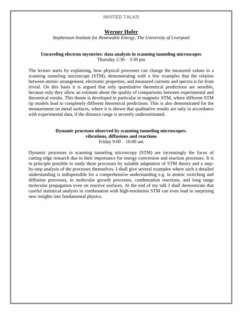
Werner Hofer Stephenson Institute for Renewable Energy, The University of Liverpool
Unraveling electron mysteries: data analysis in scanning tunneling microscopes
Thursday 2:30 – 3:30 pm
The lecture starts by explaining, how physical processes can change the measured values in a
scanning tunneling microscope (STM), demonstrating with a few examples that the relation
between atomic arrangement, electronic properties, and measured currents and spectra is far from
trivial. On this basis it is argued that only quantitative theoretical predictions are sensible,
because only they allow an estimate about the quality of comparisons between experimental and
theoretical results. This theme is developed in particular in magnetic STM, where different STM
tip models lead to completely different theoretical predictions. This is also demonstrated for the
measurement on metal surfaces, where it is shown that qualitative results are only in accordance
with experimental data, if the distance range is severely underestimated.
Dynamic processes observed by scanning tunneling microscopes:
vibrations, diffusions and reactions
Friday 9:00 – 10:00 am
Dynamic processes in scanning tunneling microscopy (STM) are increasingly the focus of
cutting edge research due to their importance for energy conversion and reaction processes. It is
in principle possible to study these processes by suitable adaptation of STM theory and a step-
by-step analysis of the processes themselves. I shall give several examples where such a detailed
understanding is indispensible for a comprehensive understanding e.g. in atomic switching and
diffusion processes, in molecular growth processes, condensation reactions, and long range
molecular propagation even on reactive surfaces. At the end of my talk I shall demonstrate that
careful statistical analysis in combination with high-resolution STM can even lead to surprising
new insights into fundamental physics.
STUDENT ORAL PRESENTATIONS
Electronic structure of graphene nanoribbons with metallic contacts Thursday 3:30 – 3:50 pm
Chloé Archambault, Alain Rochefort
École Polytechnique de Montréal, C.P. 6079, Succ. Centre-ville, Montréal, Québec, H3C 3A7
E-mail: [email protected]
Graphene is a very promising material for electronics due to its extremely high electron mobility.
Its two-dimensional structure is especially well suited for the current microfabrication
techniques. It can be made semiconducting after being engineered into nanoribbons [1, 2] such
that graphene transistors have already been reported [3, 4].
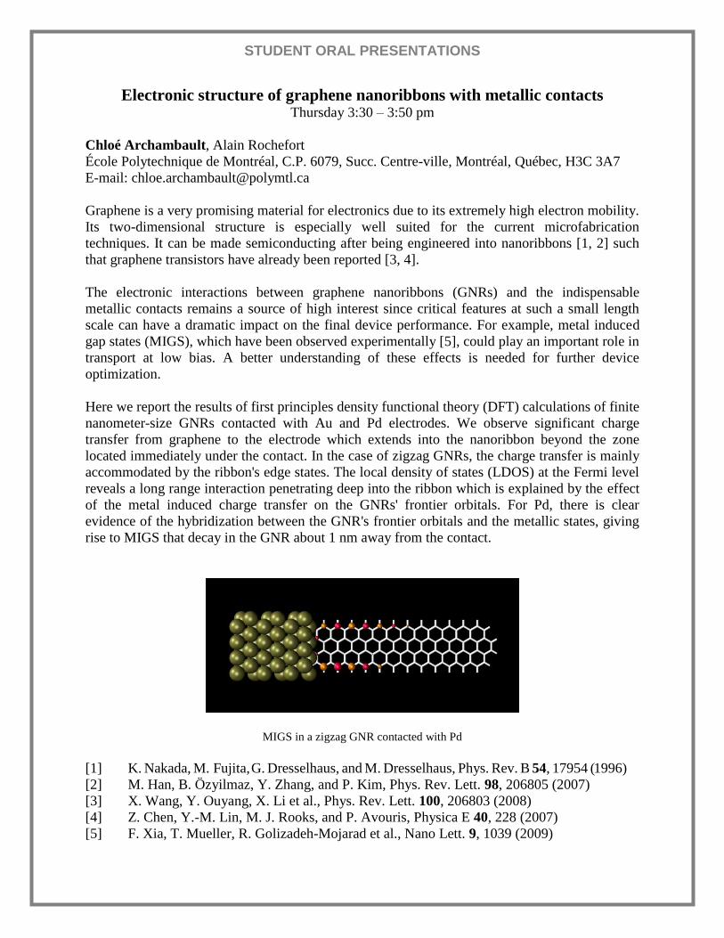
The electronic interactions between graphene nanoribbons (GNRs) and the indispensable
metallic contacts remains a source of high interest since critical features at such a small length
scale can have a dramatic impact on the final device performance. For example, metal induced
gap states (MIGS), which have been observed experimentally [5], could play an important role in
transport at low bias. A better understanding of these effects is needed for further device
optimization.
Here we report the results of first principles density functional theory (DFT) calculations of finite
nanometer-size GNRs contacted with Au and Pd electrodes. We observe significant charge
transfer from graphene to the electrode which extends into the nanoribbon beyond the zone
located immediately under the contact. In the case of zigzag GNRs, the charge transfer is mainly
accommodated by the ribbon's edge states. The local density of states (LDOS) at the Fermi level
reveals a long range interaction penetrating deep into the ribbon which is explained by the effect
of the metal induced charge transfer on the GNRs' frontier orbitals. For Pd, there is clear
evidence of the hybridization between the GNR's frontier orbitals and the metallic states, giving
rise to MIGS that decay in the GNR about 1 nm away from the contact.
MIGS in a zigzag GNR contacted with Pd
[1] K. Nakada, M. Fujita, G. Dresselhaus, and M. Dresselhaus, Phys. Rev. B 54, 17954 (1996)
[2] M. Han, B. Özyilmaz, Y. Zhang, and P. Kim, Phys. Rev. Lett. 98, 206805 (2007)
[3] X. Wang, Y. Ouyang, X. Li et al., Phys. Rev. Lett. 100, 206803 (2008)
[4] Z. Chen, Y.-M. Lin, M. J. Rooks, and P. Avouris, Physica E 40, 228 (2007)
[5] F. Xia, T. Mueller, R. Golizadeh-Mojarad et al., Nano Lett. 9, 1039 (2009)
STUDENT ORAL PRESENTATIONS
Solution of the Contact Problem of Molecular Nanoelectronics Thursday 3:50 – 4:10 pm
Firuz Demir, George Kirczenow1
Simon Fraser University
E-mail: [email protected]
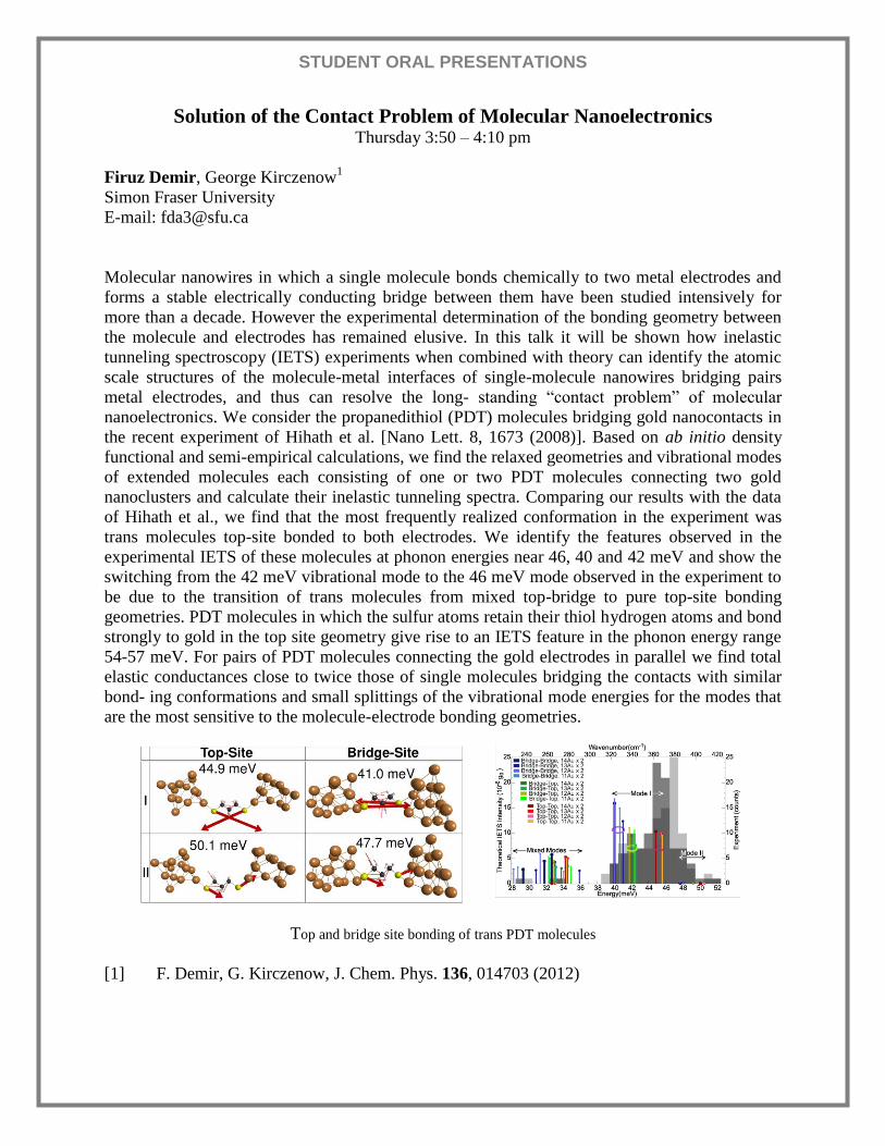
Molecular nanowires in which a single molecule bonds chemically to two metal electrodes and
forms a stable electrically conducting bridge between them have been studied intensively for
more than a decade. However the experimental determination of the bonding geometry between
the molecule and electrodes has remained elusive. In this talk it will be shown how inelastic
tunneling spectroscopy (IETS) experiments when combined with theory can identify the atomic
scale structures of the molecule-metal interfaces of single-molecule nanowires bridging pairs
metal electrodes, and thus can resolve the long- standing “contact problem” of molecular
nanoelectronics. We consider the propanedithiol (PDT) molecules bridging gold nanocontacts in
the recent experiment of Hihath et al. [Nano Lett. 8, 1673 (2008)]. Based on ab initio density
functional and semi-empirical calculations, we find the relaxed geometries and vibrational modes
of extended molecules each consisting of one or two PDT molecules connecting two gold
nanoclusters and calculate their inelastic tunneling spectra. Comparing our results with the data
of Hihath et al., we find that the most frequently realized conformation in the experiment was
trans molecules top-site bonded to both electrodes. We identify the features observed in the
experimental IETS of these molecules at phonon energies near 46, 40 and 42 meV and show the
switching from the 42 meV vibrational mode to the 46 meV mode observed in the experiment to
be due to the transition of trans molecules from mixed top-bridge to pure top-site bonding
geometries. PDT molecules in which the sulfur atoms retain their thiol hydrogen atoms and bond
strongly to gold in the top site geometry give rise to an IETS feature in the phonon energy range
54-57 meV. For pairs of PDT molecules connecting the gold electrodes in parallel we find total
elastic conductances close to twice those of single molecules bridging the contacts with similar
bond- ing conformations and small splittings of the vibrational mode energies for the modes that
are the most sensitive to the molecule-electrode bonding geometries.
Top and bridge site bonding of trans PDT molecules
[1] F. Demir, G. Kirczenow, J. Chem. Phys. 136, 014703 (2012)

STUDENT ORAL PRESENTATIONS
Magnetoresistance in Hydrogenated Graphene Thursday 4:10 – 4:30 pm
Jonathan Guillemette1, Shadi Sabri
1, Binxin Wu
1, Pierre Lévesque
2, Abdelaadim Guermoune
3,
Mohammed Siaj3, Richard Martel
2, Guillaume Gervais
1, Thomas Szkopek
1
1McGill University, Physics Department
2École Polytechnique, Départment de Génie Chimique
3Université du Québec à Montréal, Départment de Chimie
E-mail: [email protected]
Using a custom built hydrogenation gun in a UHV system, graphene samples hydrogenated to
various degrees were prepared. Room temperature resistance increases ranging from a few
percent to a 3 order of magnitude increase were achieved. The analysis of the thermal transport
of the hydrogenated graphene samples has revealed a metal insulator transition. By inserting
these samples in a 0.3K 9T magnetic field, negative magnetoresistance all the way to 9T was
found. By using the Tallahassee Magnetic Laboratory, we were able to have access to a 30T
magnet which displayed negative magnetoresistance all the way up to those magnetic fields. This
is the first report of negative magnetoresistance going all the way to 30T in hydrogenated
graphene. This disordered system can be used to explore the limits of weak and strong
localization as well as the metal – insulator transition. The investigation of the evolution of
scattering times as a function of the Fermi level of the hydrogenated graphene will be presented.
1- Variable range hopping in hydrogenated graphene
2- Normalized magnetoresistance trace at various temperatures
[1] X. Hong, S. H. Cheng, C. Herding, J. Zhu, Physical Review B 83, 085410 (2011)
[2] J. Moser et al., Physical Review B 81, 205445 (2010)
[3] Y. F. Chen et al., Journal of Physics-Condensed Matter 22, 205301 (2010)

STUDENT ORAL PRESENTATIONS
Effect of alkyl chain-length on dissociative attachment in two families of
reaction at Si(100) Friday 10:00 – 10:20 am
Maryam Ebrahimi1, Si Yue Guo, Kai Huang, Tingbin Lim, Iain R. McNab
2, Zhanyu Ning, John
C. Polanyi, Mark Shapero, and Jody (S.Y.) Yang
Department of Chemistry, University of Toronto, Toronto, ON, Canada 1Department of Chemistry, University of California, Riverside, Riverside, CA, USA
2School of Biological Sciences & Applied Chemistry, Seneca College, Toronto, ON, Canada
Presenting author E-mail: [email protected]
Corresponding author E-mail: [email protected]
We studied the dissociative attachment (D.A.), on silicon, of two families of molecules:
1-bromoalkanes and primary alcohols (which we will refer to as R-Br and R-OH, where R is a
carbon chain). The question of interest is the effect of increasing chain length, R, from C2H5 to
C5H11, on the chemical reactivity at the Si(100) surface. Each molecule was examined by
scanning tunneling microscopy (STM) at temperatures ranging from 50 K to 300 K to determine
(i) the geometry of species at the surface, (ii) the pattern of reaction to give D.A., and (iii) the
activation energy for D.A. The results were interpreted by ab initio quantum mechanical
calculation.
The three 1-bromoalkane molecules studied, bromoethane (EtBr), 1-bromopropane (PrBr), and
1-bromobutane (BuBr), were seen to physisorb and react exclusively in an inter-row
configuration on the Si(100)-c(4x2) with activation energies Ea of 0.343±0.005 eV for EtBr,
0.410±0.006 eV for PrBr, and 0.536±0.002 eV for BuBr [1]. In constrast, the three primary
alcohols, ethanol (EtOH), 1-propanol (PrOH), and 1-pentanol (PeOH), reacted exclusively on
inter-dimer sites. The energy barriers were measured to be 0.41±0.02 eV for EtOH, 0.60±0.01
eV for PrOH, and 1.004±0.007 eV for PeOH. The molecules in both families, R-Br and R-OH,
were found to have increasing activation energy for every additional carbon in the alkyl-chain.
Extensive calculations using density function theory was completed for R-Br, confirming the
increase in energy barrier by amounts comparable with the observed values. We interpret the
increase in Ea in terms of the additional energy required to lift the alkyl-chain away from the
surface, going from the initial physisorbed state to the transition state. Calculations are in
progress for R-OH.
[1] Ebrahimi, M. et al, J. Phys. Chem. C, in press (web publication on April 12, 2012)

STUDENT ORAL PRESENTATIONS
Limits of Detection for Silicon Nanowire BioFETs Friday 10:20 – 10:40 am
Nitin K. Rajan1, Xuexin Duan
2, Aleksandar Vacic
2, David A. Routenberg
2, Mark A. Reed
1,2
1Dept. of Applied Physics, Yale University, 15 Prospect St, New Haven CT06511
2Dept. of Electrical Engineering, Yale University, 15 Prospect St, New Haven CT06511
E-mail: [email protected]
Over the past decade, silicon nanowire/nanoribbon field-effect transistors (NWFETs) have
demonstrated great sensitivity to the detection of biomolecular species, with limits of detection
(LOD) down to femtomolar concentrations [1]. Several well known factors limit the LOD;
among them, ionic concentration, efficiency of the biomolecule-specific surface
functionalization, binding constants, and the delivery of the analyte to the sensor surface.
However, the signal-to-noise ratio (SNR) of these bioFET sensors, and the device parameters
that determine the LOD, are not well understood. In this work, we apply noise spectroscopy (Fig
1.) to silicon NWFETs with the goal of understanding and improving the detection limit of such
devices. Using low frequency noise measurements, we quantify the effect on device performance
of different process parameters. We also show that the SNR is maximized at maximum
transconductance (Fig 2.) due to the effects of 1/f noise, and not in the subthreshold regime
where sensitivity is maximized [2]. These devices currently have a LOD of 4 electronic charges
in ambient conditions. Using these devices, with very good performance in terms of SNR, we
were able to measure and extract the binding kinetics of protein interactions, which have never
been done with NWFETs. Binding constant determination is a critical parameter for
biomolecular design, and has until now been primarily assessed by surface plasmon resonance
(SPR). Utilizing the low LOD of these devices, we are able to extract binding constants into the
sub-picomolar range.
Fig. 1 Typical Noise Spectra for field effect
biosensors as a function of solution gate voltage.
-1.0 -0.8 -0.6 -0.4 -0.2 0.0
20000
25000
30000
35000
40000
45000
50000
55000
60000
SNR
Gm
Solution Gate Voltage Vsg
(V)
SN
R (
V-1)
0
200
400
600
800
1000
1200
gm (n
A/V
)
Fig 2. Signal-to-noise ratio plotted as a function of
solution gate voltage. Peak SNR occurs at -0.5V and
is equal to 59000 V-1
. Transconductance (gm) also
plotted as a function of solution gate bias confirming
that SNR is maximized close to the peak gm.
[1] Stern et al. Nature 445, 519-522 (2007)
[2] Rajan et al. Applied Physics Letters 97, 243501 (2010)
STUDENT POSTER PRESENTATIONS – POSTER 1
b)
A Highly Sensitive Au-string Nanoresonator as a Sensor
T.S. Biswas
1, A. Suhel
1, B.D. Hauer
1, K.S.D. Beach
1 and J.P. Davis
1, 2
1Department of Physics, University of Alberta, Edmonton, Alberta, Canada T6G 2E9
2Canadian Institute for Advanced Research, Toronto, Ontario M5G 1Z8, Canada
E-mail: [email protected]
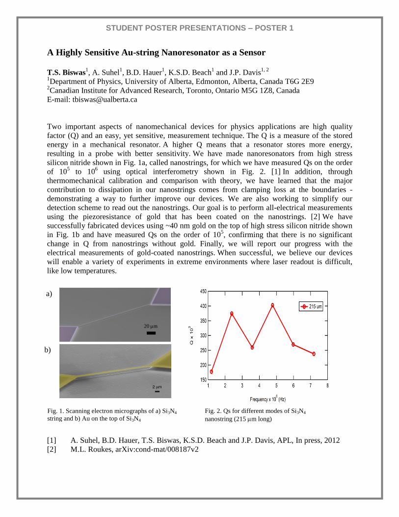
Two important aspects of nanomechanical devices for physics applications are high quality
factor (Q) and an easy, yet sensitive, measurement technique. The Q is a measure of the stored
energy in a mechanical resonator. A higher Q means that a resonator stores more energy,
resulting in a probe with better sensitivity. We have made nanoresonators from high stress
silicon nitride shown in Fig. 1a, called nanostrings, for which we have measured Qs on the order
of 105 to 10
6 using optical interferometry shown in Fig. 2. [1] In addition, through
thermomechanical calibration and comparison with theory, we have learned that the major
contribution to dissipation in our nanostrings comes from clamping loss at the boundaries -
demonstrating a way to further improve our devices. We are also working to simplify our
detection scheme to read out the nanostrings. Our goal is to perform all-electrical measurements
using the piezoresistance of gold that has been coated on the nanostrings. [2] We have
successfully fabricated devices using ~40 nm gold on the top of high stress silicon nitride shown
in Fig. 1b and have measured Qs on the order of 105, confirming that there is no significant
change in Q from nanostrings without gold. Finally, we will report our progress with the
electrical measurements of gold-coated nanostrings. When successful, we believe our devices
will enable a variety of experiments in extreme environments where laser readout is difficult,
like low temperatures.
[1] A. Suhel, B.D. Hauer, T.S. Biswas, K.S.D. Beach and J.P. Davis, APL, In press, 2012
[2] M.L. Roukes, arXiv:cond-mat/008187v2
a)
Fig. 2. Qs for different modes of Si3N4
nanostring (215 m long)
Fig. 1. Scanning electron micrographs of a) Si3N4
string and b) Au on the top of Si3N4
20 m

STUDENT POSTER PRESENTATIONS – POSTER 2
Graphene Nanomechanical Resonators
Arnab Chaudhuri1, R. Saydur Rahman
2, R. G. Knobel
3
1PhD Candidate, Queen‟s University, Canada
2Post Doctoral Fellow, Memorial University, Canada
3Associate Professor, Queen‟s University, Canada
E-mail: [email protected]
Graphene, a single atomic layer of graphite, possesses remarkable properties has drawn attention
of physicists, chemists and engineers since its extraction in 2004 [1]. Along with its fascinating
electronic properties [2], graphene because of its high Young‟s modulus, low mass, high surface
area and high quality factor (Q) (Q ~ 100000 at low temperature) [3] is an ideal candidate for
sensitive mechanical resonators. Graphene is extracted using mechanical exfoliation [4] or
chemical vapour deposition [5] transferred to Si-Si oxide substrate and then suspended graphene
device is fabricated using electron beam lithography, metal deposition to build electrodes and
substrate etching [6]. In this poster we present our progress towards realizing graphene
nanomechanical resonators for both fundamental experiments and applications as sensors. The
device is driven into vibrational motion by applying an oscillating voltage to the graphene bridge
and can be controlled by varying the back gate voltage. The readout is detected electrically by
measuring the output current through the graphene flake, which is a function of vibrational
frequency and graphene-substrate distance, using a lock in amplifier. If the temperature of the
system is lowered, the vibrational motion will tend towards quantum zero-point motion, which
will be manifested with increased visibility for graphene resonators, owing to their extremely
light mass. Tuning the driving signal introduces a duffing non-linearity, which modulates the Q
factor thus providing control over its mechanical properties [7]. Apart from these studies an
immediate application of these devices will be for ultra-sensitive mass and force detection.
[1] Novoselov et. al., Science 306, 666 (2004)
[2] Castro Neto et. al., Rev. Mod. Phys. 81, 109 (2009)
[3] Chen et. al., Nature Nanotechnology 4, 861 (2009)
[4] Geim et. al., Nature Materials 6, 183 (2007)
[5] Reina et. al., Nano Letters 9, 30-35 (2009)
[6] Bunch et al., Science 315, 490-493 (2007)
[7] Eichler et. al., Nature Nanotechnology 6, 339 (2011)

STUDENT POSTER PRESENTATIONS – POSTER 3
Thermal transport in partially unzipped carbon nanotubes
Xiaobin Chen,1 Yong Xu,
1 Bing-Lin Gu,
1 Wenhui Duan
1*
1Department of Physics, Tsinghua University, Beijing 100084, China
*E-mail: [email protected]
We report systematic investigation on the thermal properties of partially unzipped carbon
nanotubes (PUNTs) using the nonequilibrium Green's function method. It is found that thermal
conductance shows linear dependence on the central unzipped width and exponentially decays to
a finite value as the unzipped part increases. Further analysis on one dimensional atom chains
confirms that the exponential decay is due to interface scattering of the mismatched modes. Our
findings of wide-range linear controllable thermal conductance in PUNTs may help find high-
performance thermoelectric devices and the exponential decay behaviour may lead to a better
understanding of phonon transport in nanoscale systems.

STUDENT POSTER PRESENTATIONS – POSTER 4
Investigation of kinetics and growth mechanisms of graphene on copper
Saman Choubak, Pierre Levesque, Patrick Desjardins, Richard Martel
École Polytechnique, Départment de Génie Chimique
E-mail: [email protected]
Graphene, a single atomic layer of sp2-bonded carbon atoms packed to a two-dimensional
honeycomb lattice, has attracted scientists since its discovery . It is potentially a next generation
material for the electronic industry due to its novel physical and electrical properties. Graphene‟s
high carrier mobility and phenomenal optical transparency makes it an ideal material for
numerous applications in electronics, optoelectronics, biosensors, etc. In order for graphene to
become useful in practical applications, its uniform and large-area mass-production with low
defects and controlled thicknesses has become crucial.
In order to shed light to critical aspects of graphene growth mechanisms and kinetics, we are
using low energy electron microscope, (LEEM), to observe and investigate graphene nucleation
and growth mechanisms on single crystal copper. The ultimate purpose of this project is to
elucidate a viable and reproducible avenue for the production of high quality and
monocrystalline graphene films. In situ LEEM observation provides information of the processes
taking place on the surface, which allows a thorough description and understanding of growth
features. In our experiments, LEEM will serve as a tool to study graphene growth on single
crystal copper exposed to a flux of elemental carbon, atomic hydrogen, and C-based precursors.
The design of the experiments is aimed to imitate the surface kinetics involved in CVD growth
of graphene on copper foils and to gain insight into the growth mechanisms. These observations
demonstrate graphene growth from vapor-deposited carbon on the surface and the phenomenon
that occur in order for the film to nucleate and grow . This knowledge and information will allow
the control of the process in detail, whereas, otherwise stable structures may not be produced
with perfection.

STUDENT POSTER PRESENTATIONS – POSTER 5
Theory of anomalous magnetotransport in triple quantum dots
B. D’Anjou, W.A. Coish
McGill University, 3600 rue University, Montreal (QC), Canada H3A 2T8
E-mail: [email protected]
Magneto-transport measurements on a triple quantum dot ring have recently shown anomalous
quantum oscillations with dominant frequencies separated by a factor of three in magnetic flux
[1]. Such oscillations, suggestive of a one-third periodicity in the flux quantum, are usually not
observed in larger mesoscopic rings in which only larger periods are observed. We develop a
microscopic transport model for the triple dot and show that the anomalous oscillations can
dominate the transport behavior under certain conditions. Furthermore, we discuss the range of
validity of our model by studying dephasing due to broadening and electric dipole interactions.
[1] L. Gaudreau et al., Phys. Rev. B 80, 075415 (2009)
STUDENT POSTER PRESENTATIONS – POSTER 6
Structural profiling and electronic properties of pentacene on Ni(111) surface
Laurentiu Eugeniu Dinca, Jennifer MacLeod, Csaba E. Szakacs, Josh Lipton-Duffin,
Dongling Ma and Federico Rosei
INRS-EMT, 1650 boulevard Lionel-Boulet, Varennes, QC, J3X 1S2, Canada
E-mail: [email protected]
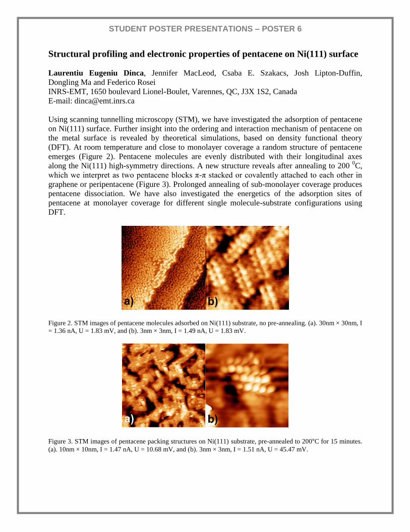
Using scanning tunnelling microscopy (STM), we have investigated the adsorption of pentacene
on Ni(111) surface. Further insight into the ordering and interaction mechanism of pentacene on
the metal surface is revealed by theoretical simulations, based on density functional theory
(DFT). At room temperature and close to monolayer coverage a random structure of pentacene
emerges (Figure 2). Pentacene molecules are evenly distributed with their longitudinal axes
along the Ni(111) high-symmetry directions. A new structure reveals after annealing to 200 0C,
which we interpret as two pentacene blocks π-π stacked or covalently attached to each other in
graphene or peripentacene (Figure 3). Prolonged annealing of sub-monolayer coverage produces
pentacene dissociation. We have also investigated the energetics of the adsorption sites of
pentacene at monolayer coverage for different single molecule-substrate configurations using
DFT.
Figure 2. STM images of pentacene molecules adsorbed on Ni(111) substrate, no pre-annealing. (a). 30nm × 30nm, I
= 1.36 nA, U = 1.83 mV, and (b). 3nm × 3nm, I = 1.49 nA, U = 1.83 mV.
Figure 3. STM images of pentacene packing structures on Ni(111) substrate, pre-annealed to 200ºC for 15 minutes.
(a). 10nm × 10nm, I = 1.47 nA, U = 10.68 mV, and (b). 3nm × 3nm, I = 1.51 nA, U = 45.47 mV.
STUDENT POSTER PRESENTATIONS – POSTER 7
Étude comparative du taux de recristallisation interfacique entre le silicium
amorphe relaxé et le silicium amorphe dé-relaxé
Ousseynou Diop, Sjoerd Roorda
Département de physique, Université de Montréal, Montréal (Québec), H3C 3J7, Canada
E-mail: [email protected]
Nous avons montré une différence entre les taux de recristallisation interfacique pour le silicium
amorphe relaxé versus celui dé-relaxé. Pour cela nous avons amorphisé deux zones distinctes sur
une gaufre de silicium cristallin en lui bombardant par des ions 28Si+. C‟est à dire on effectue
une série d‟implantations sur le c-Si avec des énergies de 2 MeV, 1 MeV et 0.5 MeV
consécutives à une fluence de 5x10¹⁵ ions/cm² chacune. Après un recuit, RTA (Rapide Thermal
Annealing) de relaxation pendant 5s à 650 °C dans un four et réimplantation d‟une zone, les
deux échantillons ont une épaisseur amorphe de (1.50±0.07) μm. La recristallisation débute à
l‟interface et s‟étend graduellement à une certaine vitesse vers la partie amorphe avec le nombre
de recuits. Une série de recuit à (500±4) °C, nous a permis de montrer que la différence entre la
zone relaxée versus dé-relaxée est significative après 4 heures de recuit et est de (0.096 ±0.007)
μm, ce qui correspond à 4.8x10¹⁷
atomes déplacés par cm2. Les taux de recristallisations sont à
l‟ordre de (2.722±0.005)×10-9
cm/s et (1.826±0.003)×10-9
cm/s respectivement dans l‟échantillon
dé-relaxé et relaxé. Soit environ 1.490±0.004 fois plus important dans l‟état dérelaxé. Ces
valeurs diminuent graduellement avec le nombre de recuits. Nous avons constaté que cette
différence de taux de recristallisation est liée à la réduction de densité de défauts supplémentaires
produits dans le silicium amorphe dérelaxé. Après le septième recuit cette différence diminue
considérablement. Ce qui veut dire que nos deux échantillons se recristallisent progressivement
avec le même taux à une légère différence de (0.14 ±0.07) x10-9
cm/s pour l‟échantillon relaxé.
STUDENT POSTER PRESENTATIONS – POSTER 8
Phase stack limit charge transport in polymer photovoltaic devices
Fei Dou1,2
, Carlos Silva2, Baozeng Wang
1, Le Kong
1, Xinping Zhang
1
1Institute of Information Photonics Technology and College of Applied Sciences,
Beijing University of Technology, Beijing 100124, China 2Département de Physique and Regroupement Québécois sur les Matériaux de Pointe, Université
de Montréal, Montréal (Québec), H3C 3J7, Canada
E-mail: [email protected]
We found the external quantum efficiency of the photovoltaic device of poly(9,9¢-
dioctylfluorene-co-bis(N,N¢- (4,butylphenyl) bis(N,N¢- phenyl -1,4- phenylene)diamine) (PFB)
and poly(9,9¢-dioctylfluorene- co-benzothiadiazole) (F8BT) can be strongly modified through
changing the mixed polymer composite ratio, which obtained the optimum at ratio 1:3 of F8BT:
PFB. After comparing the influence of charge separation and charge recombination at polymer
interface, and comparing different charge transport road at different composite ratio samples, we
proposed that not only the phase interface area, but also the phase stack configuration can largely
influence the device performance. It implies that the device performance can be improved by
better control the phase separation and phase stack through changing the blend film morphology.

STUDENT POSTER PRESENTATIONS – POSTER 9
Instrumentation and Methods for Inertial Motors used in Scanning Probe
Microscopes
Benedict Drevniok1, William M.P. Paul
2, Alastair B. McLean
1
1Department of Physics, Queen's University, Kingston, Ontario, Canada
2Department of Physics, McGill University, Montreal, QC, Canada
E-mail: [email protected]
Scanning probe microscopy continues to evolve and push the boundaries of research into basic
electronic and mechanical behaviour of surfaces and adsorbates. The ultra-high vacuum, low-
temperature, high magnetic field environments that are becoming more common in fundamental
SPM research place a unique set of demands on the instrumentation used to approach and scan a
sample. As many of the highest-performance instruments remain home-built, it is important for
wide-spread understanding of the basic building blocks of microscope operation.
We present information that will facilitate the assembly, characterization and operation of
inertial motors for modern scanning probes [1]. Specifically, a model describing the forces
required to create a step in a stick-slip type motor is developed. Simple, inexpensive drive
electronics with high slew rate and high output current are described that have been used with a
number of commercial controllers. Additionally, a novel reflective object sensor that can be used
to characterize motor performance is described. We illustrate the application of the drive
electronics and the optical sensor using a Pan-style inertial motor [2] that we have used in our
laboratory for the last three years.
[1] B. Drevniok et al., Rev. Sci. Instrum. 83, 033706 (2012)
[2] S.H. Pan et al., Rev. Sci. Instrum. 70, 1459 (1999)
STUDENT POSTER PRESENTATIONS – POSTER 10
Design and fabrication of QCA based on a SET process
G. Droulers1, S. Ecoffey
1, M. Pioro-Ladrière
2, D. Drouin
1
13IT, Université de Sherbrooke, Sherbrooke, Quebec J1K 2R1, Canada
2Départment de physique, Université de Sherbrooke, Sherbrooke, Quebec J1K 2R1, Canada
E-mail: [email protected]
As the MOSFET is further scaled down, the increase in undesirable quantum effects and the need
for better energy efficiency is driving the development of new technologies and computational
methods. The quantum cellular automata (QCA) paradigm, where two excess electrons are
confined in two of four quantum dots placed at the corners of a square, was introduced
in 1993 [1]. Since then, many theoretical and experimental demonstrations have been made.
However, room temperature operation is still a challenge especially if one wants to integrate
QCA to usable, everyday life technologies. Here, we propose a technology platform for QCA
room temperature operation. Our platform is based on the nanodamascene process [2], used for
the fabrication of single electron transistor (SET).
The first part of the project concerns the design and simulation of a clocked QCA half-cell with
SET readout (see [3]). This involves finite element method for capacitance extraction and
numerical solving of the Coulomb blockade master equations. The clocking is achieved by the
addition of a third, centered dot in the half-cell to enable a “NULL” state. The second part of the
project is to fabricate and characterize devices and demonstrate the application of the process to
these QCA principles. Intermediate devices like nanowires and metal-insulator-metal (MIM)
capacitors have been fabricated and characterized, but metal-oxide interface states remain a
challenge. Low temperature electrical characterization and devices optimisation will follow in an
attempt to raise the operating temperature. The new paradigm introduced with QCA in
combination with the present process has the potential to greatly reduce the power consumption
of future electronics and this project is a step in that direction.
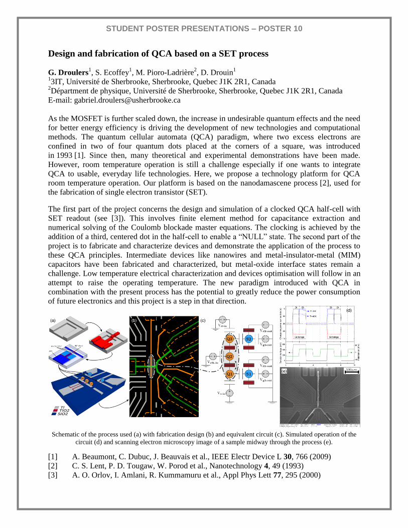
Schematic of the process used (a) with fabrication design (b) and equivalent circuit (c). Simulated operation of the
circuit (d) and scanning electron microscopy image of a sample midway through the process (e).
[1] A. Beaumont, C. Dubuc, J. Beauvais et al., IEEE Electr Device L 30, 766 (2009)
[2] C. S. Lent, P. D. Tougaw, W. Porod et al., Nanotechnology 4, 49 (1993)
[3] A. O. Orlov, I. Amlani, R. Kummamuru et al., Appl Phys Lett 77, 295 (2000)
STUDENT POSTER PRESENTATIONS – POSTER 11
Encapsulated graphene field effect transistors
S A Imam, A Guermoune, M Siaj, T Szkopek
Department of Electrical and Computer Engineering, Department of Physics, McGill University
E-mail: [email protected]
Graphene field effect transistors are fabricated on silicon oxide and silicon nitride substrates.
They are then encapsulated by 10nm thin silicon oxide and silicon nitride by room temperature
magnetron sputtering. The oxide encapsulated devices retain 55% of its bare device mobility,
while nitride retains almost 80%. Both the films result in minimal lattice degradation of
graphene, as verified by Raman Spectroscopy.

STUDENT POSTER PRESENTATIONS – POSTER 12
Characterization of Silicon Nanoribbon Debye Length Modulation using DNA
M. H. Izadi1, J. Thomas
2, X. Duan
3, D. Sen
2, P. Grutter
1, M. Reed
3
1Dept. of Physics, McGill University, Montreal, Canada
2Dept. of Molecular Biology and Biochemistry, Simon Fraser University, Burnaby, Canada
3Depts. of Elec. Eng. and Applied Physics, Yale University, New Haven, CT, USA
E-mail: [email protected]
Silicon nanoribbon field effect transistors (SiNR-FET) have the ability to sense changes in the
charge distribution of surface bound biomolecules [1] which gives them the potential to monitor
molecular charge distributions of chemical reactions in real-time. We employ DNA in order to
explore the capabilities of SiNR-FET charge detection from bound biomolecules.
SiNR-FETs can sense the molecular charge distribution of bound biomolecules with changing
ion concentration of the buffer solution. A changing ion concentration will change the Debye
screening length and thus change how much of the charge associated with the bound
biomolecules the nanoribbon „sees‟ (Figure 1).
We use duplex and triplex DNA to serve as „charge rulers‟ due to their regularly and finely
spaced negative charges along the DNA backbone (3.4 Angstroms between charges). Proper
formation of triplex DNA is confirmed using circular dichroism spectroscopy. Attachment of
DNA to silicon surfaces has been characterized using both fluorescent tagging and XPS. Initial
studies indicate effective charge screening modulation with varying salt buffer concentration.
Figure 1. SiNR-FET with duplex DNA attached. Increasing the salt buffer concentration reduces the Debye
screening length and hence the amount of attached biomolecule charge the nanoribbon „sees‟.
[1] A. Vacic, J. Criscione, N. K. Rajan, et al., J. Am. Chem. Soc. 133, 35 (2011)

STUDENT POSTER PRESENTATIONS – POSTER 13
Raising the bar on optomechanics in Davis lab
Paul H. Kim1, Bradley D. Hauer
1, Callum Doolin
1, and John P. Davis
1,2
1Department of Physics, University of Alberta, Edmonton, Alberta, Canada T6G 2G7
2Canadian Institute for Advanced Research, Toronto, Ontario, Canada M5G 1Z8
E-mail: [email protected]
Recently, there has been a breakthrough in measuring mechanical displacements of on-chip
nanomechanical devices, which has been named optomechanics [1]. This ultra-sensitive
measurement technique goes beyond the traditional interferometric scheme and is made possible
through a strong correlation between an optical cavity and a mechanical resonator. In essence, a
high quality factor for the optical cavity yields increased sensitivity for nanomechanical
detection. From advances in fabrication methods, ultra-high quality factors on the order of ~106
have been achieved using various types of Fabry-Perot, whispering gallery, and photonic cavities
[2]. Our ultimate goal is to further investigate quantum properties of nanoscale devices at low
temperatures. Our lab is currently under construction, installing two nuclear demagnetization
dilution refridgerators that will achieve lowest temperatures in Canada. After completion, I will
test various designs of nanomechanical devices, which are extensions of previously fabricated
devices in our lab [3]. We highlight our current progress towards fabricating a successful
dimpled tapered fiber, a custom machined vacuum chamber for environment control, and the
design of silicon-on-insulator optomechanical devices.
Optical image of the fabricated dimpled fiber, SEM image of the 80 m disk with a mechanical beam, and the
vacuum chamber for the apparatus.
[1] G. Anetsberger et al., arXiv:1108.4608v1, (2009)
[2] K. J. Vahala., Nature 424, 6950 (2003)
[3] J.P. Davis, et al., Appl. Phys. Lett. 96, 072513 (2010)

STUDENT POSTER PRESENTATIONS – POSTER 14
Graphene Studied by Highly Coherent Low Energy Electron Holography
A. Peter Legg, Josh Mutus, Lucian Livadaru, Radovan Urban, Jason Pitters, Robert A. Wolkow
Department of Physics, University of Alberta, 11322 89 Ave , Edmonton Alberta 1National Institute of Nanotechnology, 11421 Saskatchewan Drive, Edmonton Alberta
E-mail: [email protected]
Advances in low energy (~100 eV) in-line point projection microscopy had stalled at the ~1 nm
scale as a consequence of nano-tip emission limitations and possibly also as a result of
instrument instabilities. The recently developed nitrogen etched and stabilized tungsten nano-tip,
together with lowered mechanical noise and reduced stray magnetic perturbations have allowed a
>4 times increase in coherence angle and a virtual source size of 1.6 +/- 0.6 Angstrom, evidently
opening the door to atom-scale holographic imaging of molecules and other nano-scale entities.
Point projection microscopy will allow us to probe a graphene surface for defects as previous
experiments have shown no adverse effects from imaging. Theoretically, 3 dimensional
reconstructions of the surface are also possible which may reveal important properties invisible
to other imaging techniques.
Starting with Gabor, and by touching upon the work of other contributors to the field, the idea
and practice of point projection microscopy will be briefly reviewed. Our particular, ultra high
vacuum, instrument will be described. The instrument is at once both an atom-scale imaging
scanning tunneling microscope and a point projection microscope. The stable, reproducible and
readily repairable nitrogen etched nano-tip will be described. Results of a published study of
graphene, including observation of opacity changes with heat cleaning, and observations of ~nm
scale corrugation of suspended graphene will be shown [1]. Characterization of the electron
beam will be shown. Un-supported graphene/vacuum knife edge studies, among others, will be
described in the context of beam coherence properties. Where in the past a maximum coherence
half angle of 2 or 3 degrees had been observed [2], with the new apparatus a half coherence
angle of over 14 degrees is obtained. Some discussion of the interwoven properties of lateral and
longitudinal coherence, together with energy spread will be offered.
Graphene edge in point projection microscopy
[1] J. Y. Mutus, L. Livadaru, J. T. Robinson et al., New J. Phys. 13, 063011 (2011)
[2] Che-Cheng Chang, Hong-Shi Kuo et al., Nanotechnology, 20, 115401 (2009)

STUDENT POSTER PRESENTATIONS – POSTER 15
Ising spins on a tuneable fcc to bcc lattice
Andrew Macdonald, Sarah Burke, Doug Bonn, Yan Pennec
Depart. of Physics and Astronomy, University of British Columbia, V6T1Z4 Vancouver, Canada
E-mail: [email protected]
The study of magnetically frustrated materials has led to the discovery and control of novel
nano-scale devices [1]. A prime example is the phenomenon of exchange bias, which caused a
revolution in hard-drive read-head technology. Current research hints at further breakthroughs,
from experimental realization of ac magnetic “currents” in spin ice materials [2] to construction
of a quantum computer using magnetic qubits [3]. Future progress in frustrated magnetism will
require an strong union of experiment and theory. It is in this spirit that we report the results of a
Monte Carlo study of an Ising spin system on a tunable fcc to bcc lattice aimed at describing the
magnetic configuration of thin Cr films grown epitaxially on Au(100).
Cr has been studied extensively as the “archetypical itinerant antiferromagnet” [4]. In the early
1990s the surface of Cr(100) was the first system to be studied with spin-polarized scanning
tunneling microscopy (SP-STM), which demonstrated “topological antiferromagnetic order”
between the magnetic moments in neighbouring atomic planes [5]. In recent work at UBC it was
found that thin film fcc Cr(100) can be grown epitaxially on Au(100). An antiferromagnet on a
fcc lattice is strongly geometrically frustrated and SP-STM images of the fcc Cr(100) surface
showed that this frustration fundamentally altered the magnetic order. The surface exhibited a
complex magnetic topography with regions of ferromagnetic and antiferromagnetic order
separated by domain walls within the same [100] plane. These ordered regions were contrasted
by a breakdown of the topological order seen in bulk bcc Cr, with no apparent correlation
between spin directions in adjacent atomic terraces. The observed spin structure did not
correspond to that of a pure bcc or fcc lattice but a structure containing elements of both lattices.
To model the influence of frustration in this system computationally we employed a classical
Monte Carlo simulation of Ising pseudo-spins with nearest neighbour antiferromagnetic
exchange and single spin flip dynamics. Simulating 105 to 10
6 spins on a tuneable fcc to bcc
lattice we let the dynamics evolve with the Metropolis algorithm and examined the evolution of
the ground state as a function of the tuning parameter and simulation cell boundary conditions. A
comparison of the simulation with experiment shows strong agreement, and explains how the
inherent geometric frustration of the fcc lattice causes the breakdown of topological order
between successive atomic planes.
[1] J. P. Liu et al., Nanoscale Magnetic Materials and Applications, Springer (2009)
[2] O. Tchernyskyov, Nature New & Views 451, 22 (2008)
[3] J. Tejada, E. M. Chudnovsky, E del Barco et al. Nanotechnology 12, 181 (2001)
[4] E. Fawcett, Rev. Mod. Phys. 60, 209 (1988)
[5] R. Wiesendanger, H. J. Güntherodt et al., Phys. Rev. Lett. 65, 247 (1990)

STUDENT POSTER PRESENTATIONS – POSTER 16
Dynamics of one and two-bond dissociations of 1,2-dihaloethanes on Si(100)
Oliver MacLean, Si Yue Guo, Kai Huang, K. R. Harikumar, Amir Zabet-Khosousi, Iain
McNab1, John C. Polanyi
Department of Chemistry, University of Toronto, 80 St. George Street, Toronto, ON M5S 3H6 1Biol. Sciences and Appl. Chemistry, Seneca College, 70 The Pond Rd, Toronto, ON, M3J 3M6
Corresponding author e-mail: [email protected]
Colleagues in my group recently observed that 1,2-dichloroethane and 1,2-dibromoethane
dissociate on Si(100) in intriguingly different ways at room temperature and 110 K. At room
temperature, both carbon-halide bonds dissociate to form ethylene and a pair of halogen atoms,
with the halogen atoms bonded to Si atoms on the same dimer [1]. The ethylene is found on
average about 30 Å away from the halogen pair, which was attributed to “cartwheeling” of the
hot ethylene across the surface.
We examined the dissociation at lower temperature to investigate what further dynamics could
be in play. Surprisingly, at 110 K, only one carbon-halide bond dissociates, forming a halogen
and a haloethyl fragment [2]. Furthermore, both the physisorbed and chemisorbed features
adsorb on Si atoms that are on neighbouring rows, rather than on the same dimer as we saw at
room temperature. We suspect that the difference in reaction is a consequence of the much
slower rate of dimer flipping at 110 K relative to the room temperature rate. We are currently
working to measure activation energies for the one-bond and two-bond dissociation reactions for
both 1,2-dihaloethanes. Future work will use DFT calculations, as implemented by VASP, to
determine physisorption and chemisorption configurations, which will then used to find the
transition state using the Nudged Elastic Band method.
[1] Harikumar, K. R.; Polanyi, J. C.; Zabet-Khosousi, A.; Czekala, P.; Lin, H.; Hofer, W.
Directed long-range molecular migration energized by surface reaction, Nature
Chemistry 3, 400-408 (2011)
[2] Huang, K., Reaction Dynamics of Alkyl Bromides at Silicon; Experiment and Theory.
Ph.D. Dissertation, University of Toronto, 2011

STUDENT POSTER PRESENTATIONS – POSTER 17
Growth and properties of Graphlocons (large dendritic single graphene
crystals)
Mathieu Massicotte, Victor Yu, Eric Whiteway, and Michael Hilke
Department of Physics, McGill Universisty, Montreal, Québec H3A 2T8, Canada
E-mail: [email protected]
Graphene grown by chemical vapor deposition (CVD) on copper has attracted considerable
amount of attention due to its great potential for large scale fabrication of graphene-based
devices. However, one of the main factors limiting certain applications for CVD–graphene, is the
presence of grain boundaries of micrometer-size due to high density nucleation sites. These
domain boundaries in polycrystalline graphene reduce electronic mobilities and thermal
conductivities[1].
Hence, decreasing the number of nucleation sites and increasing the size of single grains is
important. Here, we report the growth of large dendritic-shaped and more regular shaped
graphene single-crystals (Figure 1). The crystals were grown inside a copper enclosure in order
to slow down the gas transport rate and limit the rapid surface reaction. With their sixfold
symmetry and fractal-like shape, the resulting crystals resemble snow flakes. They were found to
nucleate on copper defects and in some cases bilayers were present in the center of some
crystals. They were transferred onto a silicon oxide/silicon substrate and their lobes were
electrically contacted. The electronic properties of the devices were investigated down to sub-
Kelvin temperatures, showing mobility over 1000 cm2v
-1s
-1.
Figure 1: Graphlocon on Cu
[1] Q. Yu, L. A. Jauregui, W. Wu et al., Nature Materials 10, 443-449 (2011)

STUDENT POSTER PRESENTATIONS – POSTER 18
Ultra-short single-walled carbon nanotube NEMS transistors
Andrew C. McRae1, Joshua O. Island, Vahid Tayari, Serap Yiǧen and A.R. Champagne
2
Department of Physics, Concordia University, Montréal, Québec H4B 1R6, Canada
E-mails: [email protected],
We study electron transport in clean suspended single-wall carbon nanotube (SWCNT)
transistors hosting a single quantum dot (QD) ranging in length from 10s of nanometers down to
≈ 3 nm. Fig. 1 (a) shows a SEM image of a 70 nm breakjunction, illustrating device geometry.
To fabricate these QD devices, we align narrow gold bow-tie junctions on top of individual
SWCNTs using e-beam lithography, and suspend the devices with a buffered HF etch. We then
use a feedback-controlled electromigration to controllably open a gap in the gold junctions and
expose nm-sized sections of the SWCNTs [1]. Fig. 1 (b) shows a device with a 22 nm gap in
which the tube is visible.
We measure low temperature DC electron transport in these devices and show that they form
tunable quantum dot transistors. The Coulomb blockade characteristics show that a single QD is
housed on each nanotube. Both the stretching and bending vibronic modes are visible in
differential conductance - bias voltage - gate voltage plots of our data (Fig. 1 (c)). Despite the
bending mode‟s weak electron-vibron coupling, a high quality factor (Q) device can have a large
population of long-lived vibrons. If the current is large enough, vibron assisted electrons can then
tunnel through the QD, allowing us to directly calculate the bending frequency through DC
measurement. In our samples we find bending frequencies in the 100s of GHz range and we
calculate Q ~106. The bending frequency can controllably be tuned by tension induced by an
electrostatic or static mechanical force. These ultra-short suspended QDs are promising
candidates to develop sensitive tunable NEMS and explore the strong electron-vibron coupling
regime in SWCNTs.
Figure 1: (a) SEM image of a 70 nm nanotube connected by an electromigrated breakjunction. (b) SEM image of a
22 nm breakjunction, inset shows an enlargement of the nantotube. (c) Differential conductance data corresponding
to the device shown in (b). This data shows both stretching and bending excitations.
[1] J. Island, V. Tayari, S. Yiǧen, A. McRae and A. Champagne, App. Phys. Lett. 99,
243106 (2011)
[2] O. Usmani, Y. Blanter, and Y. Nazarov et al., Phys. Rev. B. 75, 195312 (2007)
(a)
(b) (c) (a)

STUDENT POSTER PRESENTATIONS – POSTER 19
A real space approach to DFT using finite-differences and LOBPCG
Vincent Michaud-Rioux, Hong Guo
University, Department of Physics, McGill University, Rutherford Building,
3600 rue University, Montréal (Québec), PQ H3A 2T8, Canada
E-mail: [email protected]
Ab initio atomistic calculations provide a way to achieve a microscopic understanding of
observed experimental phenomena and to make quantitative predictions of the physical
properties of nanoelectronics. In practice, atomic scale systems have irregularities (e.g. surface
roughness) or defects (e.g. substitutional atoms or vacancies) that are too strong to be ignored or
treated as small perturbations. Density functional theory[1] (DFT) is a powerful method for first
principles modelling. In Kohn-Sham density functional theory[2] (KS-DFT), a system of partial
differential equations (PDE) must be solved self-consistently. In real space techniques, the KS
Hamiltonian matrix is typically much larger but also much sparser than the matrices arising in
state-of-the-art DFT codes used in the communities of condensed matter physics, quantum
chemistry, materials science and engineering. Evidence of good performance of real space
methods - by Chebyshev filtered subspace iteration (CFSI) - was reported by Zhou et al.[3] and
such real space methods are gaining popularity[4]. Some of the reasons are that real space
computational techniques are well-suited to deal with non-symmetric systems and the locality of
real space bases results in embarrassingly parallelizable algorithms.
We report the development of a real space DFT code that calculates the electronic structure of
materials. Our code is named MatRcal which stands for "Matlab-based real space calculator". All
the terms of the Kohn-Sham Hamiltonian are projected on a three-dimensional real space mesh.
Our work indicates that the performance of the locally optimal block preconditioned conjugate
gradient method (LOGPCG) introduced by Knyazev[5] generally exceeds the performance of
CFSI for solving the KS equations. We present our implementation of a LOGPCG-based real
space electronic structure calculator and use it to compute the electronic structure of many
organic and inorganic molecules. Our results are in excellent agreement with the well established
quantum chemistry commercial code Gaussian. Our method gains in computational speed and
parallelism, but the main advantage is the possibility to handle real space boundary conditions
which is critical for future applications in nanoelectronic device modeling.
[1] P. Hohenberg, W. Kohn, Phys. Rev. 136, B864–B871 (1964)
[2] W. Kohn, L. J. Sham, Phys. Rev. 140, A1133–A1138 (1965)
[3] Y. Zhou, Y. Saad, M. L. Tiago, J. R. Chelikowsky, J. Comput. Phys. 219, 172-184 (2006)
[4] L. Lin, J. Lu, L. Ying, E. Weinan, J. Comput. Phys. 231, 2140-2154 (2012)
[5] A. Knyazev, SIAM J. Sci. Comput. 23, 517 (2001)

STUDENT POSTER PRESENTATIONS – POSTER 20
Spin pumping/transport in magnetic metal and insulator heterostructures
Eric Montoya, Bret Heinrich, Capucine Burrowes, Bartek Kardasz, Wendell Huttema, Erol
Girt
Department of Physics, Simon Fraser University, Burnaby, British Columbia, Canada
E-mail: [email protected]
Recently attention has been turned toward ideas where magnetization reversal and dynamics can
be achieved by spin transfer torque (STT) using spin polarized currents. STT devices are
intended for future nonvolatile Magnetic RAM and logic. Spin currents can come in two
flavours: spin polarized electric currents and pure spin currents. By using pure spin currents one
can avoid the perils of conventional electronics: circuit capacitance, heat generation, and electron
migration. In order to utilize pure spin currents in devices, a detailed understanding of spin
transport in normal metals is necessary. To study spin transport in Au, single layer
GaAs/16Fe/(20,300)Au and double layer GaAs/16Fe/(20,300)Au/12Fe/20Au heterostructures
were investigated using ferromagnetic resonance, where the numerals indicate the layer thickness
in atomic layers. By measuring the total Gilbert damping, α, in the 16Fe layer in the
aforementioned heterostructures as a function of temperature, we are able to determine the spin
mixing conductance, g
, at the Fe/Au interface and the spin flip relaxation time, τsf , in Au as a
function of temperature. We show that the spin flip relaxation time in Au is dominated by
phonon interactions [1]. Recently spin caloritronics posed the question; can one use spin
pumping to generate a spin current using magnetic insulators? Magnetic insulators, YIG in
particular, have very low magnetic damping allowing one to create a large number of low loss
magnons, a necessary requirement for an efficient spin pumping. We have shown that there is an
efficient transfer of spin momentum across the YIG/Au interface even when conduction
electrons in Au are fully reflected at the YIG/Au interface. We have shown that the spin
pumping efficiency of YIG films with an appropriate surface chemistry treatment is high and can
generate pure spin currents that are attractive for spintronics device applications [2,3].
[1] Eric Montoya, et al., J. Appl. Phys. 111, 07C512 (2012)
[2] B. Heinrich, et al., Phys. Rev. Lett. 107, 066604 (2011)
[3] C. Burrowes, et al., Appl. Phys. Lett. 100, 092403 (2012)

STUDENT POSTER PRESENTATIONS – POSTER 21
Vacancies in Bi2Se3: in bulk - conductance drops after 3%, in surface - robust
Vadim Nemytov, Hong Guo
Department of Physics, McGill University, Montreal, Quebec H3A 2T8, Canada
E-mail: [email protected]
3D Strong Topological Insulator (STI) has topologically protected surface states inside the bulk
gap which can carry current or spin current.[1] Bi2Se3 has been shown to be 3D STI with a
single Dirac cone and a bulk gap of ~0.2-0.3eV.[2-4] Moreover, spectroscopic study of Bi2Se3
surface state is comparable with theoretical prediction [2-4], however transport measurements
have failed to reach the predicted value of (e2/h). [5]
In experiments, vacancies might exist in the bulk and on the surface of Bi2Se3. A preliminary
transport simulation based on finite-differences method suggests that a) vacancies at random
positions throughout the sample don't affect the conductance below about 2% vacancy
concentration (VC), beyond which the conductance starts dropping rapidly b) vacancies which
reside only on top and bottom surfaces have very little effect on conductance even for relatively
high VC. The results a) strongly suggest that the topological phase breaks in the range 3-6% VC
and that surface states disappear. The results b) may be due to robustness of the topologically
protected surface states or there may be other processes at hand; it would be interesting to
compare this to other future experiments or theoretical models.
Figure 1: Conductance in Bi2Se3 Slab due to vacancies throughout the material and only on surfaces.
[1] Liang Fu, C. L. Kane, and E. J. Mele, Phys. Rev. Lett. 98, 106803 (2007)
[2] Y. Xia, D. Qian, D. Hsieh et al., Nature Physics 5, 398-402 (2009)
[3] D. Hsieh, Y. Xia, D. Qian et al., Nature 460, 1101-1105 (2009)
[4] Y. L. Chen, J. G. Analytis, J.-H. Chu, Science 325, 178-181 (2009)
[5] Desheng Kong, Judy J. Cha, Keji Lai, ACS Nano 5, 4698-4703 (2011)

STUDENT POSTER PRESENTATIONS – POSTER 22
Nanomechanical resonator circuits with atomically-thin layers
D. B. Northeast, R. Knobel
Department of Physics, Queen‟s University, Kingston, Ontario, Canada K7L 3N6
E-mail: [email protected]
Advances in nanomechanical systems [1] has allowed for the study of the motion of structures at
or near their quantum ground state for mechanical motion. Coupling these devices to resonant
electrical circuits provides not only a method of measuring with standard laboratory electronics,
but (particularly using superconducting waveguides [2]) a method for cooling towards the
ground state. Recent work [3] has recently enabled strong coupling between mechanical motion
and an LC resonator using a superconducting aluminum membrane as the mechanical element. In
this poster we propose the use of exfoliated membranes as the mechanical element, potentially
enabling a lighter resonator and stronger electromechanical coupling. Predictions based on the
use of single layers of graphene, NbSe and BSCCO are presented.
[1] J. Chan, T. P. Mayer Alegre, A. Safavi-Naeini et al., Nature 478, 7367 (2011)
[2] D. Vitali, P. Tombesi, M. J. Woolley et al., Physical Review A 76, 4 (2007)
[3] J. D. Teufel, T. Donner, D. Li et al., Nature 475, 7356 (2011)

STUDENT POSTER PRESENTATIONS – POSTER 23
Adsorption of meta-diiodobenzene on Cu(110): a theoretical study.
Chiara Panosetti, Werner A. Hofer
Surface Science Research Centre, University of Liverpool
E-mail: [email protected]
We have modeled the adsorption of 1,3-diiodobenzene (meta-diiodobenzene or m-DIB) on
Cu(110) [1] by means of Density Functional Theory as implemented in VASP [2]. We have
compared the adsorption energies of 23 possible physisorption arrangements and we have
simulated STM images for the four most stable configurations using the Tersoff-Hamann
approach [3]. We discuss the stability and relative probabilities of experimentally observing the
different structures as well as the nature of the bonding (physisorption or chemisorption) with
Density of States and charge distribution arguments. We find that the adsorption induces small
distortions in the adsorbate and in some cases an adsorption-induced symmetry breakdown
occurs. Furthermore, we find evidence that the most stable arrangement is actually a bistable
system with interesting symmetry properties.
Simulated STM images of the four most stable configurations of m-DIB on Cu(110). An overlay of the
corresponding structure is shown on the right side of each panel. The images were taken at a bias voltage of -0.2 V
and plotted as isocurrent surfaces at 0.001 pA.
[1] C. Panosetti, W. A. Hofer, J. Comput. Chem, in press (2012)
[2] G. Kresse, J. Hafner, Phys. Rev. B 47, 558 (1993)
[3] J Tersoff, D. R. Hamann, Phys. Rev. Lett. 50, 1998 (1983)

STUDENT POSTER PRESENTATIONS – POSTER 24
Implementation of atomically defined Field Ion Microscopy tips in Scanning
Probe Microscopy
William Paul, David Oliver, Mehdi El Ouali, Till Hagedorn, Yoichi Miyahara,
and Peter Grütter
McGill University Physics Department, Montréal, Québec, H3A 2T8, Canada
E-mail: [email protected]
The atomic scale geometry of scanning probe tip-sample junctions is usually unknown. Several
groups have investigated combinations Scanning Tunneling Microscopy (STM) with Field Ion
Microscopy (FIM) or Atom Probe (AP) methods in order to characterize material transfer during
adhesion or tip pulsing in STM experiments, but control over the exact atomic structure of the
tip-sample contact has yet to be demonstrated.
We employ FIM to atomically engineer the apex of a tungsten tip which is then used in a
combined STM/AFM. In order to preserve the atomic structure of the FIM prepared tip apex,
several considerable experimental challenges arise. We have developed techniques to preserve
the apex against corrosion by rest gases in UHV over long periods of time, and show that when
proper precautions are taken, an atomically defined apex can be approached to tunneling
proximity with a sample. We report results of recent experiments with atomically defined tips
from the tunneling to point contact regime performed at room temperature and at 150K on
Au(111) and other substrates.
These atomically defined tips are also used in the nanoindentation regime, where a precise
knowledge of tip geometry is needed to calculate contact area. From the contact area, we can
compute an upper bound for junction conductance based on the maximal conductivity calculated
for a W-Au interface, and attribute an additional conductance drop to scattering at defects and
disorder in the compressed junction.
(1) Tunneling to contact I(z) of W tip with Au(111) surface at 150K; (b) local tip changes
(red/green colour for adsorbed/evaporated atoms) due to contact with Au(111) near the center of
the FIM image.
(2) Nanoindentation regime where detailed knowledge of tip structure is used to set bounds on
junction conductivity (black lines). Supported by molecular dynamics and DFT calculations.
[1] A.-S. Lucier, H. Mortensen, Y. Sun & P. Grütter, Phys. Rev. B 72, 1-9 (2005)
[2] T. Hagedorn, M. El Ouali, W. Paul, D. Oliver, Y. Miyahara & P. Grütter,
Rev. Sci Instrum. 82, 113903 (2011)

STUDENT POSTER PRESENTATIONS – POSTER 25
Supramolecular Assembly of Molecules on Delta-Doped Silicon Pohl D.
1, McLean A. B.
1, Veiga R. G. A.
2, and R. H. Miwa
2
1Department of Physics, Astronomy and Engineering Physics, Queen‟s University.
2Instituto de Física, Universidade Federal de Uberlândia, Brazil.
E-mail: [email protected]
The successful manufacture of hybrid devices, that utilize the optical response or the bio-
functional properties of organic materials [1], faces the challenge of interfacing organic material
to crystalline Si because Si still dominates the semiconductor industry. However, Si surfaces are
extremely reactive and this hinders the supramolecular assembly of organic molecules. One
approach is to passivate the surfaces with Ag or Au. Our aim is to explore the possibility of using
Si surfaces that have been doped with a single atomic layer of sub-surface B [2] as a platform for
molecular self-assembly. Our methodology is to identify molecules that will assemble into
ordered layers on the template afforded by the B-passivated surface using ab initio calculation
with density functional theory and then study the adsorption and subsequent supramolecular
assembly of these molecules with STM.
In the above figure, we show an STM image collected from a Si surface that has an incompletely
formed delta doped later. On the right, we show a unit cell of the delta-doped Si surface. The
equilibrium geometry was calculated and is in good agreement with previous calculations which
show that the surface is semiconducting and that the sub-surface S5 geometry (shown) is most
stable.
[1] J. Heath, Annu. Rev. Mater. Res. 39, 1-23 (2009)
[2] A.B. McLean, L.J. Terminello and F.J. Himpsel, Phys. Rev. B 41, 7694-700 (1990)

STUDENT POSTER PRESENTATIONS – POSTER 26
Thermal Conductivity of Graphene
Serap Yigen, James Porter, Vahid Tayari, Joshua O. Island, A. R. Champagne
Concordia University, Department of Physics, Montréal, Canada
E-mail: [email protected]
We fabricated suspended graphene devices, Fig. 1(a), and measured their thermal conductivity,
, as a function of both temperature, T, and charge carrier density, n. Heat transport is a
powerful tool to obtain information about both the phononic and electronic properties of
graphene. Recent experiments on heat transport in graphene have shown a high [1], but a
detailed mapping of graphene‟s heat conductivity versus T and n is not yet available. The
measurement technique we developed is a two-point method which uses graphene as its own heat
source (Joule heating) and thermometer (resistivity). We report at temperatures ranging from
10 to 350 Kelvin, and at charge carrier densities close to the Dirac point up to about
1.51011
/cm2, in graphene crystals whose length varies from 250 nm up to one micron, Fig. 1(b).
We observed that the thermal conductivity increases by over two orders of magnitude over the
temperature range, and that it increases with the crystal‟s length [2]. can be tuned by more
than a factor of 3 with gate voltage, Fig. 1(c) [2], opening the possibility of creating room
temperature heat transistors.
1
10
100
1000
(W/m
.K)
6 7 8 9
1002 3 4
T (K)
Vgate = 0 V
l = 1 µm
l = 0.5 µm
l = 0.25 µm
1.2 μm
4
5
6
7
8
9
10
(W/m
.K)
-6 -4 -2 0 2 4 6Vgate (V)
T = 250 K
L = 0.5 µm
(a) (b) (c)
Figure 1: (a) SEM image of one of our suspended graphene device. (b) Heat conductivity, , vs T for devices
whose length varies from 250 nm to one micron. (c) vs Vgate for a 500 nm long device at T = 250K.
[1] A. A. Balandin, et al., Nano Letters 8, 902 (2008)
[2] S. Yigen, V. Tayari, J. O. Island, J. Porter, and A. R. Champagne (in preparation)

STUDENT POSTER PRESENTATIONS – POSTER 27
Designing the Electron and Spin Transport Properties of Molecular Nano-
Magnet Transistors
Fatemeh Rostamzadeh Renani, George Kirczenow
Simon Fraser University, Canada
E-mail: [email protected]
A molecular nano-magnet is a single molecule that contains transition metal atoms that endow it
with a stable magnetic moment. Transistors based on single molecule nano-magnet (SMNM) are
potential candidates for spintronic devices and information storage. Theoretical studies of
molecule nano-magnet transistors (SMNMT) have been based on simple, phenomenological spin
Hamiltonians or more complete density functional theory (DFT) calculations. This talk will
report on a tight-binding model that provides a realistic description of SMNMTs comparable to
that of DFT while being capable of treating much larger molecules. Thus it allows us to propose
ways to design the properties of SMNMT. We consider in detail some examples of Mn12 based
SMNMT in which the molecules bond to gold electrodes via thiol-terminated ligands.
For neutral and negatively charged Mn12 SMNMs with acetate or benzoate ligands the model
yields the total SMNM spin, the spins of the individual Mn ions, the magnetic easy axis
orientation, the size of the magnetic anisotropy barrier and the size of the HOMO-LUMO gap
consistent with experiments.
In experiments, the orientation of the molecule‟s easy axis relative to leads is not controllable
and it has not been feasible to measure it. Our calculations reveal the possibility of determining
the easy axis orientation experimentally by means of current measurements: We find the lowest
unoccupied molecule orbitals (LUMO) of Mn12-benzoate to be on ligands, unlike the highest
occupied molecule orbitals which is located on the Mn12magnetic core. Therefore, we predict
the transport via LUMO not to be subjected to Coulomb blockade. We predict gate controlled
switching between Coulomb blockade and coherent resonant tunneling in SMNMTs based on
such SMNMs. We propose that this effect can be used to identify specific experimentally
realized SMNMTs in which the easy axis and magnetic moment are approximately parallel to the
direction of the current flow. We also predict effective spin filtering by these SMNMs to occur at
low bias whether the transport is mediated by the HOMO that is on the magnetic core of the
SMNM or by near LUMO orbitals located on the nominally non-magnetic ligands.1
Electrons can pass through the molecular nanomagnet easily only if their spins are oriented parallel to the direction
of electric current through the molecule.
[1] F. Rostamzadeh Renani, G. Kirczenow, Phys. Rev. B 84, 180408 (2011)
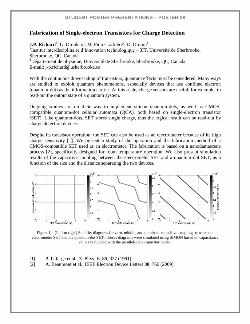
STUDENT POSTER PRESENTATIONS – POSTER 28
Fabrication of Single-electron Transistors for Charge Detection
J.P. Richard1, G. Droulers
1, M. Pioro-Ladrière
2, D. Drouin
1
1Institut interdisciplinaire d‟innovation technologique – 3IT, Université de Sherbrooke,
Sherbrooke, QC, Canada 2Département de physique, Université de Sherbrooke, Sherbrooke, QC, Canada
E-mail: [email protected]
With the continuous downscaling of transistors, quantum effects must be considered. Many ways
are studied to exploit quantum phenomenons, especially devices that use confined electron
(quantum-dot) as the information carrier. At this scale, charge sensors are useful, for example, to
read-out the output state of a quantum system.
Ongoing studies are on their way to implement silicon quantum-dots, as well as CMOS-
compatible quantum-dot cellular automata (QCA), both based on single-electron transistor
(SET). Like quantum-dots, SET stores single charge, thus the logical result can be read-out by
charge detection devices.
Despite its transistor operation, the SET can also be used as an electrometer because of its high
charge sensitivity [1]. We present a study of the operation and the fabrication method of a
CMOS-compatible SET used as an electrometer. The fabrication is based on a nanodamascene
process [2], specifically designed for room temperature operation. We also present simulation
results of the capacitive coupling between the electrometer SET and a quantum-dot SET, as a
function of the size and the distance separating the two devices.
Figure 1 – (Left to right) Stability diagrams for zero, middle, and dominant capacitive coupling between the
electrometer SET and the quantum-dot SET. Theses diagrams were simulated using SIMON based on capacitance
values calculated with the parallel-plate capacitor model.
[1] P. Lafarge et al., Z. Phys. B. 85, 327 (1991)
[2] A. Beaumont et al., IEEE Electron Device Letters 30, 766 (2009)

STUDENT POSTER PRESENTATIONS – POSTER 29
Modelling of electrical percolation in size distributed carbon nanostructures
networks
Simoneau L-P., Rochefort A.
École Polytechnique de Montréal, Engineering Physics Department
Regroupement québécois sur les matériaux de pointe (RQMP)
E-mail: [email protected]
Electronic display and photovoltaic devices typically rely on the use of transparent electrodes,
which are in their great majority rigid, brittle and expensive. An alternative that would not
possess those drawbacks is thus highly desirable and the properties of percolative networks of
carbon nanotubes (CNT) or graphene nanoribbons (GNR) place them among the most promising
candidates to reach this goal. Computational means are well suited for the description of the
underlying physics and the optimization of the characteristics of such nanostructures networks,
but previous efforts in this direction typically consider a single parameter to describe the CNT-
CNT junctions [1], which is in fact the limiting factor the propagation of charge carriers [2].
We have developed Monte Carlo (MC) algorithms to study the charge transport in bi- and
tridimensionnal networks of CNT and GNR by incorporating realistic distributions and
descriptions of CNT-CNT (or GNR-GNR) junctions. Our MC algorithms generate random
networks with many controlled parameters which can be tuned to represent experimental
networks of CNTs, GNRs or some mixture of different nanostructures. We then evaluate the total
conductance of the generated networks on the basis of individual contacts conductance, which in
turn depend on the local network properties. Our results show that the length, diameter,
orientation and chirality distributions within the percolative network of the CNT and GNR
networks have a great importance on the resulting electrical performances. By varying the
contact resistances distributions, we reproduce experimental results for CNTs networks [3].
[1] Hicks J, Behnam A, Ural A. Physical Review E 79, 012102 (2009)
[2] Nirmalraj PN, Lyons PE, De S, Coleman JN, Boland JJ. Nano Letters 9, 3890 (2009)
[3] Aguirre CM. Ph.D. Thesis (2007)

STUDENT POSTER PRESENTATIONS – POSTER 30
Modeling of Clocked Molecular-scale Quantum-dot Cellular Automata
Beyond the Mean-field Approximation
Marco Taucer
1, Faizal Karim
2, Konrad Walus
2, Robert A. Wolkow
1
1Dept of Physics, University of Alberta, T6G 2E1, Edmonton, AB
2Dept of Electrical and Computer Engineering, University of British Columbia, Vancouver, BC
V6T 1Z4
E-mail: [email protected]
Quantum-dot Cellular Automata (QCA) provides a basis for classical computation without
transistors. QCA cells consist of tunnel-coupled quantum dots with mobile electrons, and
information is encoded in the positions of electrons within each cell.
In this talk, I will present computational results that treat small groups of QCA cells with a
Hamiltonian analogous to a quantum mechanical Ising-like spin chain in a transverse field. These
simulations include the effects of inter-cellular entanglement whereas many previous QCA
simulations relied upon the so-called Intercellular Hartree Approximation (ICHA), which
neglects the possibility of entanglement[1]. When energy relaxation is included in the model, we
find that intercellular entanglement changes the qualitative behaviour of the system. Specifically,
certain schemes for memory and for clocked QCA architectures, which are predicted to work on
the basis of the ICHA, do not work when entanglement is accounted for. The ICHA is a valid
approximation in the limit of very low tunneling rates, which are realized in lithographically
defined quantum-dots[2]. However, in molecular-scale QCA[3], entanglement may play a role.
The degree to which entanglement poses a problem for memory and clocking depends upon the
interaction of the system with its environment, as well as the system‟s internal dynamics.
[1] J. Timler and C. S. Lent, J. Appl. Phys. 19, 823 (2002)
[2] I. Amlani, A. O. Orlov, G. Toth et al., Science 283, 289-291 (1999)
[3] M. B. Haider, J. L. Pitters, G. A. DiLabio et al., Phys, Rev. Lett. 102, 046805 (2009)

STUDENT POSTER PRESENTATIONS – POSTER 31
Fabrication of nanometer-scale suspended graphene transistors
Vahid Tayari, Joshua O. Island, Serap Yiğen, James Porter, A.R.Champagne,
Department of Physics, Concordia University, Montreal, Quebec, Canada
E-mails: [email protected] , [email protected]
We present a method to fabricate suspended ultra-short graphene transistors. We define narrow
bowtie gold junctions on exfoliated graphene, and use oxygen plasma to etch away the graphene
not masked by the gold junctions. The junctions are suspended using a wet etch. We use a
feedback-control electromigration procedure to open a nm size gap in the gold bridge to expose
sections of graphene which are 100 to 300 nm wide, and as short as ≈10 nm Fig. (a). Using
electron transport, we measure conductance in these suspended graphene nanocrystals as a
function of temperature and charge carrier density Fig. (b) and observe near ballistic transport.
These ultra-short transistors offer the prospect of exploring the coupling between flexural
vibrons and charge carriers in graphene and developing ultra high frequency NEMS.
Fig. (a): Suspended gold bridge with nanometer size graphene crystal. Fig. (b):
Conductance of a ≈7nm long graphene crystal with width of ≈100nm as a function
of gate voltage which controls charge carrier density. µ=1800cm2/Vs at n=10
11/cm
2
and T=4.2K.
[1] J. O. Island, V. Tayari, et al., App. Phys. Lett 99; 243106 (2011)
[2] Hongkun Park, Andrew K. L. Lim, Jiwoong Park, et al., App. Phys. Lett 75, 301 (1999)
[3] J. Scott Bunch, Arend M. van der Zande, et al., Science 315, 5811 (2007)
Graphene
Source Drain
Gate
(a) (b)

STUDENT POSTER PRESENTATIONS – POSTER 32
Growth of MgO and NaCl thin insulating films on iron surfaces
Antoni Tekiel, Jessica Topple, Shawn Fostner, Yoichi Miyahara, Peter Grütter
Department of Physics, McGill University, Montreal, H3A 2T8, Canada
E-mail: [email protected]
Thin insulating films grown on a variety of metal substrates, such as Ag(001), Mo(001) and
Fe(001), are frequently used in systems where the film serves as a tunnelling barrier directly
controlling properties of a device. For example in heterogeneous catalysis and magnetoelectronic
devices the insulating film is often made of magnesium oxide that can be grown layer by layer
allowing for control of the tunnelling barrier thickness. However, well-defined and fully
crystalline MgO thin layers are difficult to fabricate and are usually oxygen deficient. These
difficulties have been attributed to the MgO-metal lattice mismatch and the fact that in ultra-high
vacuum (UHV), regardless the preparation method, MgO is essentially grown from two separate
sources of magnesium and oxygen, which have to react on the substrate to nucleate MgO.
In this work, we characterize the morphology of MgO and NaCl thin films on Fe(001) surfaces
by UHV atomic force microscopy (NC-AFM) and low energy electron diffraction (LEED). First,
to determine the possibilities for quality improvement of MgO films grown on iron we choose
reactive deposition method, which gives full control over the gaseous species existing in the
evaporated beam. We demonstrate that it can produce much larger terraces of up to 20 nm (on an
8 monolayer thick film) compared to other methods [1,2]. Second, we investigate the
morphology and orientation of NaCl thin films grown on clean Fe(001) and oxygen passivated
Fe(001)-p(1x1)O surfaces, with the former system identified recently as an alternative tunnelling
barrier in magnetic tunnelling junctions [3]. Contrary to MgO, growth of NaCl proceeds from
molecular dimers, and thus is much better controlled due to reduced complexity of on surface
NaCl nucleation. We discuss the effects of the temperature and the oxygen presence on the
growth and demonstrate that on the oxygen passivated surface NaCl can be grown in a layer-by-
layer mode providing atomically flat films with 40-60 nm wide terraces and with much less
defects than the MgO films.
[1] M. Klaua et al., Phys. Rev. B 64 134411 (2001)
[2] M. Mizuguchia et al., Appl. Phys. Lett. 88 251901 (2006)
[3] P. Vlaic, J. Magn. Magn. Mater. 322 1438 (2010)

STUDENT POSTER PRESENTATIONS – POSTER 33
Short channel low field impurity mobility in graphene from first principles
Zi Wang1, Hong Guo
2, Kirk H. Bevan
1
1Department of Materials Engineering, McGill University, Montreal, QC H3A 2B2, Canada
2Department of Physics, McGill University, Montreal, QC H3A 2T8, Canada
E-mail: [email protected]
The remarkable properties of graphene have been studied extensively since its discovery in 2004
[1,2]. Due to its very high carrier mobility, graphene has attracted considerable interest in high-
performance radio frequency (r.f.) applications [3]. Since graphene is a surface, from a
topological perspective, it will interact with any environment: substrate adatoms, imperfections,
and impurities all act as disordered scattering sites on the graphene surface, and it is believed that
defect scattering is the dominant scattering mechanism in graphene [4,5]. The present work uses
the first-principles non-equilibrium Green's function (NEGF) formalism to study the effects of
dopant disorder on carrier mobility in graphene devices. More specifically, this theory
incorporates the contributions from diffusive impurity scattering [6]. This term is typically
assumed to be negligible in transport studies of short channel devices, where current flow is
assumed to be ballistic. However, here we show that diffusive impurity scattering can play a
crucial role in the conduction properties of wide short channel device materials (such as
graphene). The results of this study could substantially impact upon the design of ultra-high
frequency graphene r.f.-devices, where short channels on the order of tens of nanometers are
needed to modulate current flow [3].
A graphene two-probe device. One possible path of an electron undergoing diffusive scattering is shown.
[1] A. K. Geim and K. S. Novoselov, Nat. Mater. 6, 183 (2007)
[2] A. K. Geim, Science 324, 1530 (2009)
[3] Y.Wu, Y.-m. Lin, A. A. Bol, et al., Nature 472, 74 (2011)
[4] K. S. Novoselov, A. K. Geim, S. V. Morozov et al., Nature 438, 197 (2005)
[5] J.-H. Chen, C. Jang, S. Xiao, et al., Nat. Nano. 3, 206 (2008)
[6] Y. Ke, K. Xia, and H. Guo, Phys. Rev. Lett. 100, 166805 (2008)

MONTREAL ATTRACTIONS
Close to McGill
Restaurants
Lola Rosa (vegetarian bistro, $12-20)
537 Milton (corner Aylmer)
Offering tasty & hearty vegetarian meals: burritos, quesadillas, lasagne, curries. Also serves
nachos and beer. One of the most tasty restaurants near McGill.
Pizza Il Focolaio ($13-20)
1223 Rue Du Square Phillips (just south of St-Catherine St)
This wood fired pizzeria always draws a large crowd - don‟t be discouraged, the service is
incredibly quick. One of Montreal‟s top pizzas.
Amelios Pizza ($10-20)
201 Rue Milton (corner Sainte-Famille)
A bring your own wine restaurant that‟s a legend in the area. Serves up well priced fresh pasta
and pizza.
Coffee
Pikolo Espresso Bar
3418 B Avenue du Parc (between Sherbrooke and Milton)
Great coffees and tasty baked snacks. A real gem in the neighbourhood.
There are also several large coffee chains nearby: Starbucks (Union/Ontario; University/de
Maisonneuve; Eaton center), Second Cup (Milton/Parc), Presse Cafe (Milton/Parc), Tim Hortons
(Parc between Sherbrooke and Milton; Sherbrooke/University)
Bars
Benelux (brewpub)
245 Rue Sherbrooke Ouest (corner Jeanne-Mance)
Benelux offers many excellent beers primarily in the Belgian and American styles.
Olde Orchard (Irish Pub)
20 Rue Prince Arthur Ouest (corner St-Laurent)
Standard Irish Pub fare.
Pullman (Wine Bar)
3424 Avenue du Parc (between Sherbrooke and Milton)
Their sommeliers will delight in finding you something really exciting to try. Grab a flight of
three wines for a tasting. Great selection of snacks and cheeses.

Liquor Stores
Beer and table wine can be bought at any grocery store or dépanneur (convenience store) until
11pm (known as “Beer O‟Clock”) in Quebec.
The SAQ provincial liquor commission has many outlets in the downtown area including one at
the Galeries Du Parc underground mall (connected to New Residence Hall).
Grocery Stores
Can be found in the Galeries Du Parc mall: Metro is a large grocery store chain. You can buy
excellent fruits and vegetables at Eden in the same mall.
Iconic Montreal Food
Smoked Meat
The Main (24 hrs)
3864 St-Laurent (between des Pins and Duluth)
Across the street from the iconic Schwartz‟, this is where real Montrealers go for their smoked
meat at any hour of the day. On the scale of lean to fatty, order a medium at the very least.
Bagels
Fairmount (24 hrs)
74 Fairmount Ouest (1.5 blocks east of Parc avenue)
Montreal‟s first bagel bakery, opening in 1919. Montreal‟s best bagel. Nearby: Dieu Du Ciel.
Rotisserie Chicken
Romados 115 Rachel Est (3 blocks east of St-Laurent)
Charcoal grilled Portuguese rotisserie chicken. Take it for a picnic in Jeanne-Mance Park, where
Rachel ends 6 blocks West of here (the City of Montreal allows the consumption of alcohol in
parks as long as one is having a picnic where picnic tables exist).
Poutine
La Banquise (24 hrs)
994 Rachel Est
This is the poutine place, if you‟re looking for it. Fries, cheese curds, and gravy of the highest
quality (100% vegetarian options available). Lots of styles to suit any poutine craving, any time
of day. Don‟t get a large unless you‟re dared to.
Beer
Dieu Du Ciel
29 Avenue Laurier Ouest (accessible from 80 du Parc bus or Laurier metro)
Montreal‟s most renowned brewpub. Always creating fantastic offerings, but can be unpleasantly
busy at night – get there early, or late (after 11pm). Fairmount bagels are just around the corner
to help soak up the excess beer for a classic Montreal night...

Places to Visit
Mount Royal
There are several convenient ways to visit the Mount Royal park from New Residence Hall. Two
popular ways to get to the Chemin Olmstead (a pedestrian & bicycle gravel road that runs
through the park) are shown in this map: http://g.co/maps/ktkep. Once you‟re in the park, you
can visit the Chalet (look-out) for a nice view over downtown Montreal. This is about 10 minutes
walk from the entrance at Peel & des Pins if you take the stairs up.
Old Montreal
Vieux-Montréal is one of the most beautiful, well-preserved vibrant “old towns” in North
America. You can get there by walking from McGill Campus through Place des Arts and
Montreal China Town. The old town starts once you cross St. Antoine Street. Walk on Notre-
Dame and St. Paul Streets from Place d'Armes to Place Jacques-Cartier. Make sure to see the
Notre-Dame Basilica, the City Hall, the Bonsecours Market and of course the Old Port of
Montréal.
Montreal Museum of Fine Arts (Musée des Beaux-Arts)
One of Canada's most famous museums, this popular institution houses a wide collection of
international contemporary and Canadian exhibits, and straddles two buildings, the 1912 original
and its 1991 across-the-street annex with underground galleries that connect the two sites.
Admission to the Museum's collection is free at all times, but the main exhibition (Beyond Pop:
Tom Wesselmann) costs, which is half price ($7.5) on Wednesday nights, from 5 to 8 p.m. for
adults. Note that the Museum's collection is closed after 5 p.m. To get there, walk west on
Sherbrooke Street. The museum is just 10 minutes walk away from McGill University campus.

La Ronde
Six Flags operates Canada‟s second largest amusement park on St Helen‟s Island. It is home to
10 roller coasters, and a total of 40 rides. Among them, Le Monstre is the largest wooden roller
coaster in Canada, and at 39.9 meters, currently holds the record for tallest two-track roller
coaster in the world. La Ronde can be easily reached by Metro to Jean-Drapeau station on St
Helen‟s island, where there is a bus to help get you there faster (the park is a 15-20 min walk
from the metro station). On the topic of molecular electronics, while visiting St Helen‟s Island,
go see the fabulous pentagons and hexagons of Buckminster Fuller‟s dome, built for Expo ‟67!
Olympic Stadium – Biodôme – Jardin Botanique
A Metro ride out to Viau or Pie-IX (they are very close together) will take you to these
attractions. The Olympic Stadium might not be that attractive, but the view from the top of the
tower is cool. If you‟re into observing penguins, monkeys, bats, beavers, alligators and other
animals all under one roof, check out the Biodôme where you can explore indoor replicas of four
ecosystems found in the Americas. The Jardin Botanique is just around the corner and “ranks as
one of the world‟s largest and most spectacular botanical gardens.”
Bixi
Montreal‟s self-serve bicycle rental network costs $7 for 24 hr access or $15 for 72 hr access by
credit card. Once you have access, you can borrow the bicycles as often as you wish from any
station on the network, but only for 30 minute rides: Heavy fines start accruing nearly
exponentially with time after the initial 30 minutes. For longer trips, dock the bike after short
stretches and you can take another after a 2 minute delay. If a station is full, you can get a 15
minute extension to find another one to dock the bike by inserting your credit card at the terminal
and following the directions. See the map of the Bixi network at http://montreal.bixi.com
Markets
The Marché Atwater is located at the south end of Avenue Atwater, near the Lachine Canal.
You can get to it by Bixi (check the map online for exact station locations) or by Metro to
Lionel-Groulx station. The market has many local produce vendors, restaurants, bakeries, and
butchers. A major highlight is the Fromagerie Atwater cheese shop. The Marché Jean-Talon
(accessible near Metro Jean-Talon) is much larger, with ~3x the number of vendors of glorious
local products. Lots of things to taste on site.
Tam-tams and Medieval Foam Fighters
On Sunday afternoons a large drum circle forms at the George-Étienne Cartier monument
(Mount Royal Park, on the Park Avenue side, where Rachel would intersect Park). It has
become one of the main tourist attractions of the city. People assemble in the park around the
monument to relax, tan, play frisbee, and smoke. The Medieval Foam Fighters usually battle it
out with their foam swords and spears nearby in the woods of the park. These warriors are very
kind and may offer you a sword to borrow for combat.

A
BCD
EF

A
McConnell Engineering Bldg3480 rue University, room 13
Rutherford Physics Building3600 rue University, board room
Trottier Building3630 rue University, lobby
New Residence Hall3625 avenue du Parc, lobby
Centre Mont-Royal2200 rue Mansfield
Restaurant L'Academie2100 rue Crescent
B
C
D
E
F
Rue Crescent
Rue Crescent
Mansfield St
Mansfield St
UNION
“Mon
trea
lN
orth
”
“Mon
trea
lN
orth
”
UNION
747
BU
S
PLACE DU FRÈRE-ANDRÉ
747
BU
S
PLACE DU FRÈRE-ANDRÉ
AIR
PO
RT
AIR
PO
RT
500m500m
JEANNE-MANCE
JEANNE-MANCE