profile estimation Sequential measurement strategy for...
13
This article was downloaded by: [Virginia Tech Libraries] On: 17 May 2014, At: 14:39 Publisher: Taylor & Francis Informa Ltd Registered in England and Wales Registered Number: 1072954 Registered office: Mortimer House, 37-41 Mortimer Street, London W1T 3JH, UK IIE Transactions Publication details, including instructions for authors and subscription information: http://www.tandfonline.com/loi/uiie20 Sequential measurement strategy for wafer geometric profile estimation Ran Jin a , Chia-Jung Chang a & Jianjun Shi a a H. Milton Stewart School of Industrial and Systems Engineering , Georgia Institute of Technology , 765 Ferst Drive NW, Atlanta , GA , 30332 , USA Accepted author version posted online: 24 May 2011.Published online: 07 Nov 2011. To cite this article: Ran Jin , Chia-Jung Chang & Jianjun Shi (2012) Sequential measurement strategy for wafer geometric profile estimation, IIE Transactions, 44:1, 1-12, DOI: 10.1080/0740817X.2011.557030 To link to this article: http://dx.doi.org/10.1080/0740817X.2011.557030 PLEASE SCROLL DOWN FOR ARTICLE Taylor & Francis makes every effort to ensure the accuracy of all the information (the “Content”) contained in the publications on our platform. However, Taylor & Francis, our agents, and our licensors make no representations or warranties whatsoever as to the accuracy, completeness, or suitability for any purpose of the Content. Any opinions and views expressed in this publication are the opinions and views of the authors, and are not the views of or endorsed by Taylor & Francis. The accuracy of the Content should not be relied upon and should be independently verified with primary sources of information. Taylor and Francis shall not be liable for any losses, actions, claims, proceedings, demands, costs, expenses, damages, and other liabilities whatsoever or howsoever caused arising directly or indirectly in connection with, in relation to or arising out of the use of the Content. This article may be used for research, teaching, and private study purposes. Any substantial or systematic reproduction, redistribution, reselling, loan, sub-licensing, systematic supply, or distribution in any form to anyone is expressly forbidden. Terms & Conditions of access and use can be found at http:// www.tandfonline.com/page/terms-and-conditions
-
Upload
hoangthuan -
Category
Documents
-
view
212 -
download
0
Transcript of profile estimation Sequential measurement strategy for...

This article was downloaded by: [Virginia Tech Libraries]On: 17 May 2014, At: 14:39Publisher: Taylor & FrancisInforma Ltd Registered in England and Wales Registered Number: 1072954 Registered office: Mortimer House,37-41 Mortimer Street, London W1T 3JH, UK
IIE TransactionsPublication details, including instructions for authors and subscription information:http://www.tandfonline.com/loi/uiie20
Sequential measurement strategy for wafer geometricprofile estimationRan Jin a , Chia-Jung Chang a & Jianjun Shi aa H. Milton Stewart School of Industrial and Systems Engineering , Georgia Institute ofTechnology , 765 Ferst Drive NW, Atlanta , GA , 30332 , USAAccepted author version posted online: 24 May 2011.Published online: 07 Nov 2011.
To cite this article: Ran Jin , Chia-Jung Chang & Jianjun Shi (2012) Sequential measurement strategy for wafer geometricprofile estimation, IIE Transactions, 44:1, 1-12, DOI: 10.1080/0740817X.2011.557030
To link to this article: http://dx.doi.org/10.1080/0740817X.2011.557030
PLEASE SCROLL DOWN FOR ARTICLE
Taylor & Francis makes every effort to ensure the accuracy of all the information (the “Content”) containedin the publications on our platform. However, Taylor & Francis, our agents, and our licensors make norepresentations or warranties whatsoever as to the accuracy, completeness, or suitability for any purpose of theContent. Any opinions and views expressed in this publication are the opinions and views of the authors, andare not the views of or endorsed by Taylor & Francis. The accuracy of the Content should not be relied upon andshould be independently verified with primary sources of information. Taylor and Francis shall not be liable forany losses, actions, claims, proceedings, demands, costs, expenses, damages, and other liabilities whatsoeveror howsoever caused arising directly or indirectly in connection with, in relation to or arising out of the use ofthe Content.
This article may be used for research, teaching, and private study purposes. Any substantial or systematicreproduction, redistribution, reselling, loan, sub-licensing, systematic supply, or distribution in anyform to anyone is expressly forbidden. Terms & Conditions of access and use can be found at http://www.tandfonline.com/page/terms-and-conditions
IIE Transactions (2012) 44, 1–12Copyright C© “IIE”ISSN: 0740-817X print / 1545-8830 onlineDOI: 10.1080/0740817X.2011.557030
Sequential measurement strategy for wafer geometric profileestimation
RAN JIN, CHIA-JUNG CHANG and JIANJUN SHI∗
H. Milton Stewart School of Industrial and Systems Engineering, Georgia Institute of Technology, 765 Ferst Drive NW, Atlanta, GA30332, USAE-mail: [email protected]
Received April 2010 and accepted December 2010
The geometric profile, factors such as thickness, flatness, and local warp, are important quality features for a wafer. Fast and accuratemeasurements of those features are crucial in multistage wafer manufacturing processes to ensure product quality, process monitoring,and quality improvement. The current wafer profile measurement schemes are time-consuming and are essentially an offline technologyand hence are unable to provide a quick assessment of wafer quality. This article proposes a sequential measurement strategy to reducethe number of samples measured in wafers while still providing an adequate accuracy for quality feature estimation. In the proposedapproach, initial samples are measured and then a Gaussian process model is used to fit the measured data and generate a trueprofile of the measured wafer. The profile prediction and its uncertainty serve as guidelines to determine the measurement locationsfor the next sampling iteration. The measurement stops when the prediction error of the testing sample set satisfies a pre-designatedaccuracy requirement. A case study is provided to illustrate the procedures and effectiveness of the proposed methods based on thewafer thickness profile measurement in slicing processes.
Keywords: Gaussian process model, inspection, sampling, semiconductor industry, sequential measurement
1. Introduction
In semiconductor manufacturing, the geometric shape ofa wafer is an important index that can be used to evaluateits quality. For example, the profile can be used to estimatequality variables defined by the Semiconductor Equipmentand Materials International as industrial standards, suchas Total Thickness Variation (TTV), Bow, and Warp. Thesevariables are not only used as measures of the quality of thefinal wafer but also to identify root the causes of surfaceimperfections created during a production (Pei et al., 2003;Pei et al., 2004; Zhu and Kao, 2005). Also, the geometricprofiles of wafers are modeled to obtain the optimal val-ues of process variables in a wafer manufacturing process(Zhao et al., 2011). This requires online measurement of awafer’s geometric profiles in order to obtain relevant andtimely information. This timely information is required ifeffective process control of a wafer manufacturing processis to be obtained. Unfortunately, current measuring proce-dures are time-consuming and are unable to provide waferprofile information in a timely manner. For example, theexisting wafer measurement technologies, such as touchingprobe–type sensors, take more than 8 hours to measure a
∗Corresponding author
typical batch of wafers (e.g., 400 wafers in one productionrun). Time-consuming measurements prevent the imple-mentation of advanced process monitoring and diagnosistechnologies for quality improvement. Therefore, the ob-jective of this article is to develop an efficient and system-atic measurement strategy to reduce the measurement timeusing a sequential sampling and modeling approach. Wepropose to minimize a composite index that is based on themeasured sample size and times for the model fittings asthe efficiency improvement index:
Comp.Index = τntotal
max(ntotal)+ (1 − τ )Itotal
max(Itotal), (1)
where ntotal is the total sample size measured for a wafer,Itotal is the total time for the model fitting in the measure-ment strategy, τ is a weighting coefficient that evaluatesthe measurement time for each point and the computationtime, and max(ntotal) and max(Itotal) are the maximum ofthe total sample size and total time of model fittings fora batch of wafers, which are used to normalize the effectsof sample size and number of model fittings. If the sameaccuracy is created with a smaller composite index, thenwe consider the measurement strategy to have a higherefficiency.
High-definition geometric profiles of each wafer are mea-sured during the wafer manufacturing process. There are
0740-817X C© 2012 “IIE”
Dow
nloa
ded
by [
Vir
gini
a T
ech
Lib
rari
es]
at 1
4:39
17
May
201
4

2 Jin et al.
numerous methods to model the geometric profiles pre-sented in the literature. From an engineering perspective,physical analytical models, such as finite element analysisor partial differential equations, are adopted to model thegeometric profiles (Zhang and Kapoor, 1990; Abburi andDixit, 2006; Ozcelik and Bayramoglu, 2006; Huang andGao, 2010). A major limitation of these methods is thatthey require a sophisticated understanding of the forma-tion of the profile. Another limitation is that these methodsare usually used to model a deterministic profile and there-fore they have limited capabilities to model the randomnessof the profile errors or the random field effects. Some otherapproaches, such as methods in computer graphics, usespline (Forsey and Bartels, 1988; Lee et al., 1997; Sederberget al., 2004) or wavelet analysis (Schroder, 1996; Valette andProst, 2004) to model the profile data. In most cases, poten-tial factors that could influence the shape or characteristicsare not considered in the profile modeling.
In this article, a Gaussian Process (GP) model is usedto characterize the spatially correlated geometric shape ofa wafer, including the profile mean, correlated variability,and measurement noise. One of the advantages of the pro-posed GP model is that the correlated variability can befurther decomposed into global variability and local vari-ability components that can be easily interpretated. Globalvariability represents the trend in variation over the wholewafer, whereas local variability captures the variation onlywithin a small region around the measurement locations.An optimal sampling scheme is required to implement GPmodels. In the spatial statistics approach, the grid spac-ing determination approach has been applied to reduce thesample size. By maximizing the grid space, the samplingcost can be minimized in an optimal sampling scheme un-der the constraints of an allowed maximum error variance(Curran and Williamson, 1986; Curran, 1988). Anotherapproach to determine the optimal grid spacing design forsampling multiple variables is to use the conditional krig-ing variance based on cross-correlations among variables(McBratney and Webster, 1983a, 1983b; Atkinson et al.,1992, 1994). In addition the relationships between the esti-mation accuracy of the response variable and the requiredsample size have been explored and investigated (Wang etal., 2005; Xiao et al., 2005). However, a major limitation ofthese sampling strategies is that the local spatial variabilityin the response variable is neglected. Variable grid spac-ing approaches have been developed that address this defi-ciency (Anderson et al., 2006). In this approach a smallergrid space is determined in regions with higher local vari-ability, which is equivalent to measuring more samples inthat region and vice versa. There are measurement strate-gies that are based on sequentially allocating the samplesbased on prior information. This type of strategy is widelyused in optimal sensor selection and allocation problems. Inthe optimal sensor selection or allocation problem, poste-rior distributions based on prior measurements are used todetermine the sensor location that maximizes the informa-
tion gain. When it is difficult to evaluate an exact posteriordistribution, the Sequential Monte Carlo (SMC) methodis used for numerical approximation. The SMC methodhas shown a powerful ability to solve both sophisticatedstatistical problems and engineering applications (Liu andChen, 1998; Doucet et al., 2000; Doucet et al., 2001). TheBayesian SMC method has been used to solve the opti-mal sensor selection problem and target tracking and lo-calization problems (Guo and Wang, 2004). However, theperformance of this method depends on the existance ofan appropriate parametric form of the Bayesian model,and it is generally computationally intensive for posteriorcalculations.
The sequential design approach found in computer ex-periments in CEs is another type sampling strategy that hasbeen extensively used to optimize input variables (Schonlauet al., 1998; Williams et al., 2000; Park et al., 2002; Kleijnenand Van Beers, 2004; Huang et al., 2006). One of the ob-jectives of the sequential design approach is to reduce thenumber of experimental runs required to reach the opti-mal solution, which refers to minimum or maximum of theresponse. A sequential measurement design strategy hasbeen proposed that sequentially allocates more samplingpoints at the locations with a higher Expected Improve-ment (EI) to allow the minimum of an investigated surfaceto be reached quickly (Williams et al., 2000). A larger EI im-provement is defined as locations with a smaller predictedvalue or a larger predicted variance for the minimization ofa problem.
Other than focusing on minimizing the required experi-mental runs to obtain the optimal solution, there are otherGP-based sequential sampling approaches that focus onhow to sample sequentially in order to obtain an improvedmodel fitting, conditional on the new pair of sample points.These models are usually obtained from the posterior distri-butions via a Markov Chain Monte Carlo approach. Var-ious thrifty criteria–based sequential sampling problemscan be found in MacKay (1992), Cohn (1996), and Mulleret al. (2004). Some sequential applications have been shownto approximate static optimal designs (Seo et al. 2000; Gra-macy and Lee, 2009).
Optimal sampling schemes and sequential designs pro-vide effective ways to reduce the sample size by solving aset of optimization problems. However, some of these ap-proaches are computationally intensive and others are notapplicable in online measurement situations. For grid spac-ing determination, the chosen sample locations are not di-rectly associated with locations with higher local variabilitywithin each grid. In the sequential design approach, somemethods are targeted at optimization objectives, which isnot the same as for online measurements. Moreover, mostof the sampling schemes and existing sequential measure-ments involve computationally intensive optimization pro-cedures to determine additional samples.
This article continues the stream of sequential de-sign in CEs to measure samples sequentially, called a
Dow
nloa
ded
by [
Vir
gini
a T
ech
Lib
rari
es]
at 1
4:39
17
May
201
4
Sequential measurements of wafer profile 3
sequential measurement strategy, but differs in the followingways. First, the proposed sampling scheme aims to simul-taneously consider both the global variation trend and thelocal variability pattern to achieve a more accurate predic-tion ability. Second, prior engineering knowledge on theinput–output relationships is taken into account to deter-mine the initial measurement samples. By combining thesetwo aspects, the proposed sequential measurement strategyenhances the wafer quality profile prediction performancewith a higher efficiency. Although the proposed frameworkis similar to the sequential design approach, the innova-tion of this article lies in two proposed empirical distri-butions for initial measurements and sequential measure-ments, which will be discussed in detail later in this article.
The rest of this article is organized as follows. The GP-based sequential measurement strategy is described in de-tail in Section 2. A case study on wafer thickness profileestimation is provided in Section 3 to evaluate the pro-posed measurement strategy. Finally, the conclusions andfuture work directions are summarized in Section 4.
2. GP-based sequential measurement strategy
2.1. Overview of the sequential measurement strategy
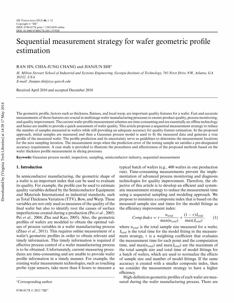
The framework of the proposed sequential measurementstrategy is shown in Fig. 1.
In the proposed methodology, all measurement loca-tions are determined by sampling empirical distributions.The empirical distributions are the estimated probabilitydensity functions evaluated at discrete potential measure-ment locations. The sequential measurement strategy startsto sample an empirical distribution based on engineeringknowledge and then fits a GP model that is based on theinitial measurements. In the estimation, the measured lo-cations are partitioned into a training sample set and atesting sample set. A GP model is estimated based on thetraining sample set and the model accuracy is evaluatedbased on the testing sample set. If the stopping rule is satis-fied, the iterative measurement procedure stops; otherwise,additional samples are measured to further improve the es-timation performance. In this approach, the magnitude ofthe gradient and the predicted Mean Squared Error (MSE)from the previous GP model are used to determine the se-
quential measurements. By iteratively taking the samplesand re-fitting the model, the GP models are expected tobetter approximate the true wafer profile.
2.2. Measurement locations and data format
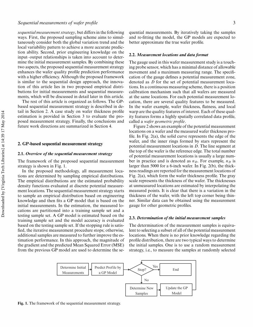
The gauge used in this wafer measurement study is a touch-ing probe sensor, which has a minimal distance of allowablemovement and a maximum measuring range. The specifi-cation of the gauge defines a potential measurement zone,denoted as D for the set of potential measurement loca-tions. In a continuous measuring scheme, there is a positioncalibration mechanism such that all wafers are measuredat the same locations. For each potential measurement lo-cation, there are several quality features to be measured.In the wafer example, wafer thickness, flatness, and localwarp are the quality features of interest. Each of these qual-ity features forms a highly spatially correlated data profile,called a wafer geometric profile.
Figure 2 shows an example of the potential measurementlocations on a wafer and the measured wafer thickness pro-file. In Fig. 2(a), the solid curve represents the edge of thewafer, and the inner rings formed by stars represent thepotential measurement locations in D. The line segment atthe top of the wafer is the reference edge. The total numberof potential measurement locations is usually a large num-ber in practice and is denoted as nD. For example, nD islarger than 5000 for a 6-inch wafer. In Fig. 2(b), the thick-ness readings are reported for the measurement locations ofFig. 2(a), which form the wafer thickness profile. The grayscale represents the thickness of the wafer. The thicknessesat unmeasured locations are estimated by interpolating themeasured points. It is clear that there is a variation in thethickness of the wafer, with the left top corner being thin-ner. Similar data can be obtained using the measurementgauge for other geometric profiles.
2.3. Determination of the initial measurement samples
The determination of the measurement samples is equiva-lent to selecting a subset of all of the potential measurementlocations. When there is no prior knowledge regarding theprofile distribution, there are two typical ways to determinethe initial samples. One is to use a random measurementstrategy, i.e., to measure the samples at randomly selected
Determine New
Samples
End
No
Stop?
Update the GP
Model
Determine Initial
Measurements
Predict Profile by
a GP Model
Yes
Fig. 1. The framework of the sequential measurement strategy.
Dow
nloa
ded
by [
Vir
gini
a T
ech
Lib
rari
es]
at 1
4:39
17
May
201
4
4 Jin et al.
Fig. 2. Potential measurement points and measurement result (a) potential measurement locations and (b) thickness profile.
locations; the other way is to view the initial measurementsamples as a design in a CE and then incorporate a LatinHypercube Design (LHD) or uniform design with spacefilling criteria to define sample locations (Santner et al.,2003).
The random measurement approach is straightforwardand easy to implement; however, a major limitation of thisapproach is that initial samples may be too close together.Since the wafer profile is spatially correlated, such sampleswithin a region will not only have a high correlation andhence contribute little information toward better fitting butmay also may create a singularity when correlation matrixesare inverted in the model estimation process (Santner et al.,2003).
The space filling design approach has an advantage inCEs over the random sampling strategy in that it in-creases the distance between pairs of points in an initialdesign. However, this approach can be difficult to imple-ment in regions with irregular shapes, as is the case forthe potential measurement points on a wafer consideredin this article. Other typical forms of space filling designchoose the design points mainly based on the distancesbetween the input variables, which ignores the relation-ship between response (profile) and input variables (loca-tions). In this case, the design may be inefficient, especiallywhen input–output relationships are available based onengineering knowledge. More advanced techniques mayuse these input–output relationships in a more complexmanner (Santner et al., 2003). Therefore, this article pro-poses a computationally efficient approach by samplinga weighted empirical distribution based on engineeringknowledge.
To efficiently determine the measurement samples,the local variability of a wafer profile is defined asfollows.
Definition 1. Local variability of a wafer profile. The localvariability of a wafer profile at location x is the samplevariance of the profile values at the measured locations
within a region �(x):
σ 2Y(x) = 1
nx − 1
∑x′∈�(x)
(Y(x′) − Y(x′))2 (2)
where x′ is a location within the region around of x, Y(x′) isthe sample mean of the profile values in the region, and nxis the sample size region. The region �(x) is defined as thekth nearest neighborhood. Generally, k is chosen to have avalue of at least 25 so that a good estimation of variancecan be guaranteed.
To determine efficient initial measurement samples, re-gions that potentially have a higher local variability shouldhave more samples taken from them, as in the grid spac-ing determination approach (Anderson et al., 2006). Inthe wafer manufacturing process, the ideal wafer profilehas a uniform thickness. Unfortunately, observed thick-ness values deviate from the ideal profile, which has aset of potential root cause factors, denoted as U(x) ={u1(x), . . . , uq(x)}. Here, the ui (x)(i = 1, 2, . . . , q) are thepotential factors associated with the wafer locations, suchas the contact span at x. The local variability of the profilehas a proportional relationship to its potential factors fromthe engineering perception and is verified by the data:
σ 2Y(x) ∝
∏q1i=1 uti
i (x)∏qj=q1+1 utj
j (x)(3)
where∏q1
i=1 utii (x) is the product of the factors that
are proportional to the local variability of the profile,∏qj=q1+1 uti
j (x) is the product of factors that are inverselyproportional to local variability of the profiles (there areq1 proportional factors and (q − q1) inversely proportionalfactors), and ti and tj are the powers for each factor.
Based on the proportional relationship in Equation (3),the initial measurement points are determined by samplingan empirical distribution defined as
Pr(x) = 1c1
∏q1i=1 uti
i (x)∏qj=q1+1 utj
j (x)(4)
Dow
nloa
ded
by [
Vir
gini
a T
ech
Lib
rari
es]
at 1
4:39
17
May
201
4

Sequential measurements of wafer profile 5
where c1 is the corresponding normalizing constant.By sampling the empirical distribution defined in Equa-
tion (4), the sample locations with larger local variabilitywill have a higher probability to be selected as the initialmeasurements. The detailed procedure can be summarizedas follows:
Step 1. Obtain the proportional relationship between thelocal variability of the wafer profile and its potentialfactors as in Equation (3).
Step 2. Estimate the empirical distribution for the initialmeasurement using Equation (4).
Step 3. Determine the sample size n0 and allocate the sam-ple sizes to circles, so that they are proportional tothe summation of the probability of the points onthat circle.
Step 4. Sample the points from the outermost circle to theinnermost circle one by one. For each circle, thepoints are sampled G times, and the samples areselected to have max–min distances to the sampleson the outer circles.
Step 5. Measure the wafer profile at the locations deter-mined in Step 4.
In this procedure, we use stratified sampling and a max–mincriterion to determine initial measurements from the outer-most circle to the innermost circle. The max–min criterionis
max min∀x1∈Cir1,∀x2∈Cir2‖x1 − x2‖2 (5)
where Cir1 and Cir2 are the sets of locations of the outercircle and the inner circle in Step 4.
2.4. GP models for the geometric profile of a wafer
Based on the measurements, a GP model is adopted tomodel the geometric profile of a wafer:
Y(x) = fT(x)β+ Z(x) + ε (6)
where fT(x)β represents the mean part of the wafer pro-file; in general, the basis functions fT(x) = [ f1(·), . . . , fp(·)]are known; β = [β1, . . . , βp]T is the regression coefficientvector; Z(x) is a Gaussian process with mean zero and co-variance function σ 2
Zψ ; σ 2Z is the variance of the covariance
function, which represents the wafer profile fluctuationcaused by manufacturing error; and ε is the uncorrelatednoise term and follows a normal distribution NID(0, σ 2
∈),which represents the measurement noise. Note that the cor-relation function used is an anisotropic Gaussian correla-tion function that has the form
ψ(x j , xk) = exp
(−
p∑i=1
φi (xi j − xik)2
)(7)
where φi is the scale parameter associated with the ith pre-dictor;� = [φ1, . . . , φp]; and p is the dimension of the inputvariables. In the wafer profile estimation problem, x j is the
jth location on the wafer with coordinate (x1 j , x2 j ), andp = 2. To be more specific, x1 j is the axis parallel to the ref-erence edge of a wafer, and x2 j is the axis perpendicular tothe reference edge of a wafer. The origin is at the geometriccenter of the wafer.
In the wafer profile estimation problem, we use an ordi-nary kriging model to fit the wafer’s geometric profile:
Y(x) = β0 + Z(x), (8)
where β0 is the constant mean part. This simplification isbased on the facts that (i) a GP model with a constantmean part can adequately model the wafer profile; and (ii)the measurement noise of the wafer profile ε is negligiblecompared with the profile accuracy requirement.
This model is obtained in the following way. We partitionthe measured samples into a training sample set {xi , Yi }nTr
i=1,and a testing sample set {xi , Yi }nTr +nTe
i=nTr +1. Based on the train-ing sample set, the predicted profile at an unobserved loca-tion x is obtained by the ordinary kriging predictor as
Y(x) = β0 + ψ(x)T�−1(Y − β01) (9)
where 1 is a nTr × 1 vector with all elements equal to 1;ψ(x)T = [ψ(x − x1)ψ(x − x2) . . . ψ(x − xnTr )]; ψ is a ma-trix with elements ψ(x j − xk) in the row j and column k;Y = Y1,Y2, . . . ,YnTr T; and β0 = 1T�−1Y/1T�−11. TheY(x) is the best linear unbiased estimator that interpolatesall the measured locations (Santner et al., 2003).
In the parameter estimation, the scale parameter � isestimated by Maximum Likelihood Estimation (MLE), de-noted as �. Then � is plugged into Equation (9) to calculateβ0 (Santner et al., 2003). In this way, a predicted profile isobtained by changing x in Equation (9). When there are ad-ditional samples collected in new iterations, the unknownparameters are re-estimated, and a new profile for the lo-cations of interest is predicted with the updated ordinarykriging model.
2.5. Determination of sequential samples
The samples are measured sequentially so that the sam-ples collected at later measurement iterations can be ap-propriately selected based on prior information from theGP model. If the stopping rule is not satisfied, the mea-surement of the (i+ 1)th iteration is required based on theGP model in the ith iteration. We propose to sample anempirical distribution, weighted by the magnitude of thegradient and predicted MSE of the GP model.
Denote the predicted GP response as Yi (x) in the ithiteration, the gradient of the predicted GP as dYi (x) withthe magnitude |dYi (x)|, and the MSE at any location x asErri (x), then we have (Lophaven et al., 2002)
dYi (x) = ∂ pYi (x)∂x1, ∂x2, . . . , ∂xp
,
Dow
nloa
ded
by [
Vir
gini
a T
ech
Lib
rari
es]
at 1
4:39
17
May
201
4
6 Jin et al.
and
Erri (x) = σ 2Z(1 + (1T�−1ψ(x) − 1)T(1�−11)−1
(1T�−1ψ(x) − 1) − ψ(x)T�−1ψ(x)).
Then the samples of the (i+ 1)th iteration are sampledfrom the following empirical distribution:
Pr(x) = 1c2
{λ
( |dYi (x)|c3
)+ (1 − λ)
(Erri (x)
c4
)}(10)
where λ is a weighting coefficient, which is a tuning param-eter; c2 is a normalizing constant for the distribution; andc3 and c4 are the maximum values of the magnitude of thegradient and prediction error, respectively, which are usedto standardize the magnitude of the gradient and predic-tion error. In Equation (10), the first part represents thearea with a large fluctuation, and the second part repre-sents the area with a large prediction uncertainty. Moremeasurements in these two types of local areas lead to areduction in the prediction error since the ordinary krig-ing model interpolates these extra measurements. Recallthat when two sampled locations are close to one another,their correlation may become high. In addition, for a largesample size the maximum distance between any two sam-pled locations is reduced. These points mean that a higherprediction accuracy can be achieved.
In practice, the distance between measurements shouldbe larger than a minimal distance to avoid the singularityproblem when computing the inverse of the correlationmatrix. In other words, measurements will not be taken atsampling locations that are too close to previously sampledlocations.
2.6. Stopping rule
In the sequential measurement strategy, the samples aremeasured sequentially until a stopping rule is satisfied. Inmost cases, the Root Mean Sum of the Prediction Error(RMSPE) of a profile is used to evaluate the overall profileprediction accuracy. It is defined as
RMSPE =√√√√1
n
n∑i=1
(Y(xi ) − Y(xi ))2 (11)
where Y(xi ) is the predicted profile at the location xi fromthe estimated GP model and n is the number of measure-ments that are compared.
It is ideal to evaluate the RMSPE of samples that arenot used in modeling. In order to estimate the RMSPEof the overall wafer profile, we compute the testing errorbased on the testing sample set collected in each measure-ment iteration to determine if the measurement stops. Themeasurement will stop if
RMSPEtesti ≤
√Thσ 2 (12)
where Thσ 2 is a pre-determined estimation variance thatrepresents the profile accuracy requirement. In this article.RMSPEtest
i is the root mean sum of the testing sample setin the ith measurement iteration.
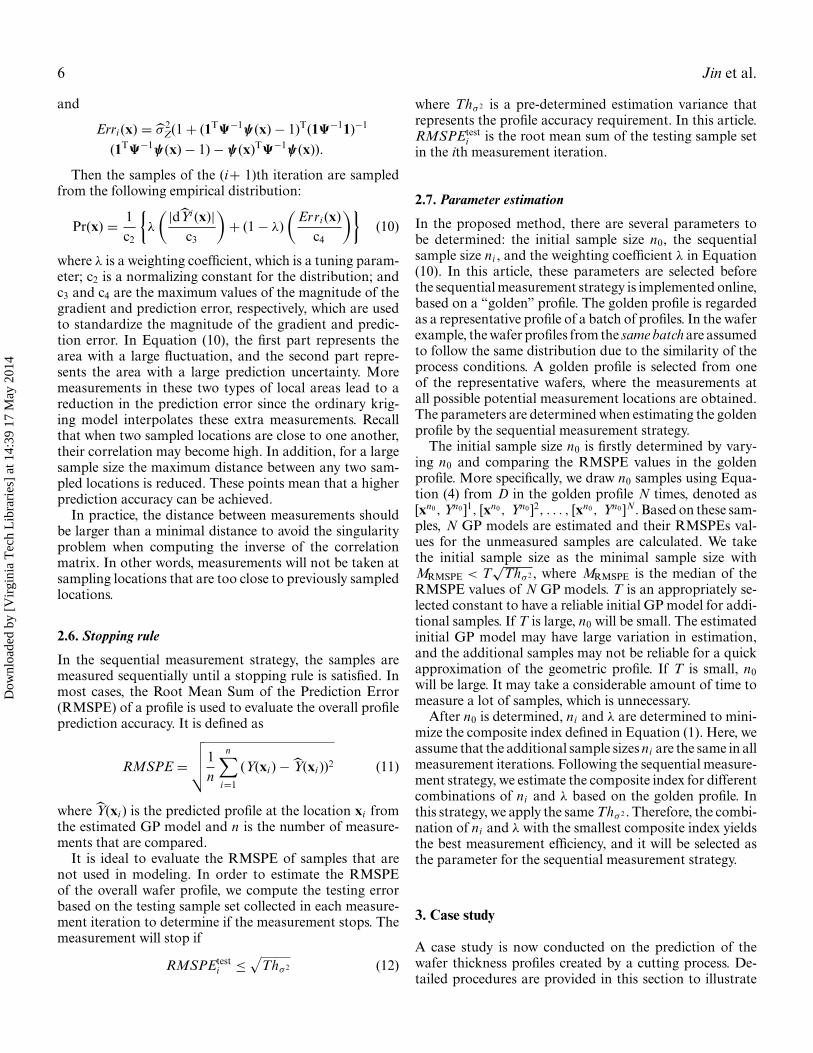
2.7. Parameter estimation
In the proposed method, there are several parameters tobe determined: the initial sample size n0, the sequentialsample size ni , and the weighting coefficient λ in Equation(10). In this article, these parameters are selected beforethe sequential measurement strategy is implemented online,based on a “golden” profile. The golden profile is regardedas a representative profile of a batch of profiles. In the waferexample, the wafer profiles from the same batch are assumedto follow the same distribution due to the similarity of theprocess conditions. A golden profile is selected from oneof the representative wafers, where the measurements atall possible potential measurement locations are obtained.The parameters are determined when estimating the goldenprofile by the sequential measurement strategy.
The initial sample size n0 is firstly determined by vary-ing n0 and comparing the RMSPE values in the goldenprofile. More specifically, we draw n0 samples using Equa-tion (4) from D in the golden profile N times, denoted as[xn0,Yn0 ]1, [xn0, Yn0 ]2, . . . , [xn0, Yn0 ]N. Based on these sam-ples, N GP models are estimated and their RMSPEs val-ues for the unmeasured samples are calculated. We takethe initial sample size as the minimal sample size withMRMSPE < T
√Thσ 2 , where MRMSPE is the median of the
RMSPE values of N GP models. T is an appropriately se-lected constant to have a reliable initial GP model for addi-tional samples. If T is large, n0 will be small. The estimatedinitial GP model may have large variation in estimation,and the additional samples may not be reliable for a quickapproximation of the geometric profile. If T is small, n0will be large. It may take a considerable amount of time tomeasure a lot of samples, which is unnecessary.
After n0 is determined, ni and λ are determined to mini-mize the composite index defined in Equation (1). Here, weassume that the additional sample sizes ni are the same in allmeasurement iterations. Following the sequential measure-ment strategy, we estimate the composite index for differentcombinations of ni and λ based on the golden profile. Inthis strategy, we apply the same Thσ 2 . Therefore, the combi-nation of ni and λ with the smallest composite index yieldsthe best measurement efficiency, and it will be selected asthe parameter for the sequential measurement strategy.
3. Case study
A case study is now conducted on the prediction of thewafer thickness profiles created by a cutting process. De-tailed procedures are provided in this section to illustrate
Dow
nloa
ded
by [
Vir
gini
a T
ech
Lib
rari
es]
at 1
4:39
17
May
201
4
Sequential measurements of wafer profile 7
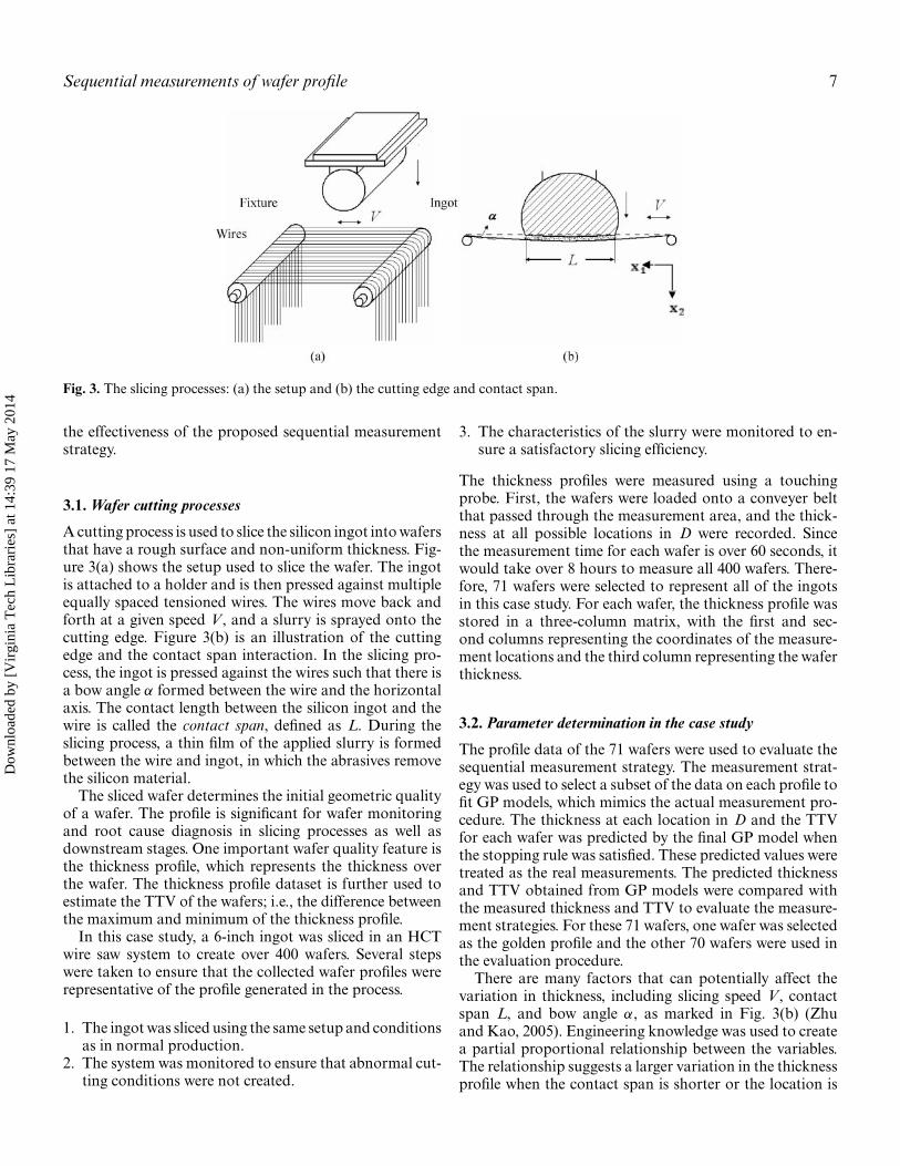
Fig. 3. The slicing processes: (a) the setup and (b) the cutting edge and contact span.
the effectiveness of the proposed sequential measurementstrategy.
3.1. Wafer cutting processes
A cutting process is used to slice the silicon ingot into wafersthat have a rough surface and non-uniform thickness. Fig-ure 3(a) shows the setup used to slice the wafer. The ingotis attached to a holder and is then pressed against multipleequally spaced tensioned wires. The wires move back andforth at a given speed V, and a slurry is sprayed onto thecutting edge. Figure 3(b) is an illustration of the cuttingedge and the contact span interaction. In the slicing pro-cess, the ingot is pressed against the wires such that there isa bow angle α formed between the wire and the horizontalaxis. The contact length between the silicon ingot and thewire is called the contact span, defined as L. During theslicing process, a thin film of the applied slurry is formedbetween the wire and ingot, in which the abrasives removethe silicon material.
The sliced wafer determines the initial geometric qualityof a wafer. The profile is significant for wafer monitoringand root cause diagnosis in slicing processes as well asdownstream stages. One important wafer quality feature isthe thickness profile, which represents the thickness overthe wafer. The thickness profile dataset is further used toestimate the TTV of the wafers; i.e., the difference betweenthe maximum and minimum of the thickness profile.
In this case study, a 6-inch ingot was sliced in an HCTwire saw system to create over 400 wafers. Several stepswere taken to ensure that the collected wafer profiles wererepresentative of the profile generated in the process.
1. The ingot was sliced using the same setup and conditionsas in normal production.
2. The system was monitored to ensure that abnormal cut-ting conditions were not created.
3. The characteristics of the slurry were monitored to en-sure a satisfactory slicing efficiency.
The thickness profiles were measured using a touchingprobe. First, the wafers were loaded onto a conveyer beltthat passed through the measurement area, and the thick-ness at all possible locations in D were recorded. Sincethe measurement time for each wafer is over 60 seconds, itwould take over 8 hours to measure all 400 wafers. There-fore, 71 wafers were selected to represent all of the ingotsin this case study. For each wafer, the thickness profile wasstored in a three-column matrix, with the first and sec-ond columns representing the coordinates of the measure-ment locations and the third column representing the waferthickness.
3.2. Parameter determination in the case study
The profile data of the 71 wafers were used to evaluate thesequential measurement strategy. The measurement strat-egy was used to select a subset of the data on each profile tofit GP models, which mimics the actual measurement pro-cedure. The thickness at each location in D and the TTVfor each wafer was predicted by the final GP model whenthe stopping rule was satisfied. These predicted values weretreated as the real measurements. The predicted thicknessand TTV obtained from GP models were compared withthe measured thickness and TTV to evaluate the measure-ment strategies. For these 71 wafers, one wafer was selectedas the golden profile and the other 70 wafers were used inthe evaluation procedure.
There are many factors that can potentially affect thevariation in thickness, including slicing speed V, contactspan L, and bow angle α, as marked in Fig. 3(b) (Zhuand Kao, 2005). Engineering knowledge was used to createa partial proportional relationship between the variables.The relationship suggests a larger variation in the thicknessprofile when the contact span is shorter or the location is
Dow
nloa
ded
by [
Vir
gini
a T
ech
Lib
rari
es]
at 1
4:39
17
May
201
4
8 Jin et al.
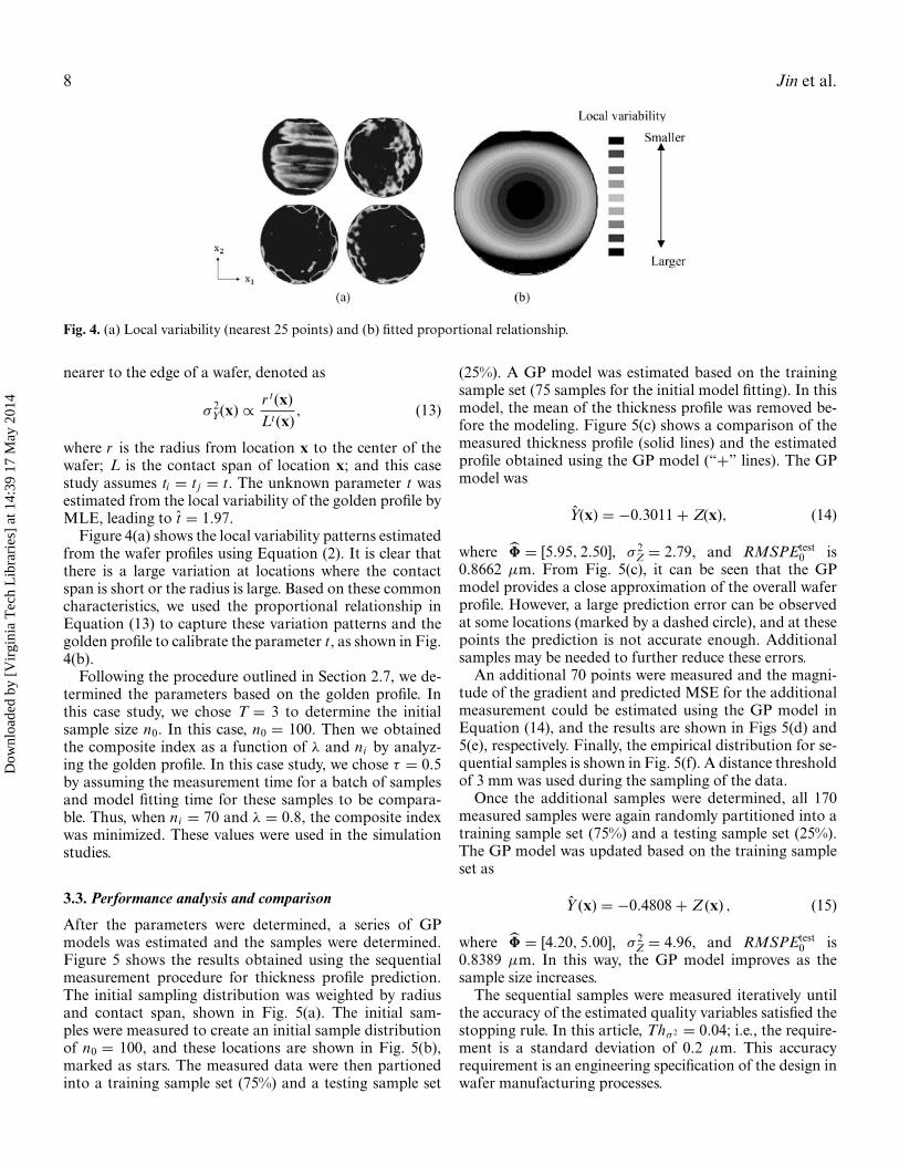
Fig. 4. (a) Local variability (nearest 25 points) and (b) fitted proportional relationship.
nearer to the edge of a wafer, denoted as
σ 2Y(x) ∝ r t(x)
Lt(x), (13)
where r is the radius from location x to the center of thewafer; L is the contact span of location x; and this casestudy assumes ti = tj = t. The unknown parameter t wasestimated from the local variability of the golden profile byMLE, leading to t = 1.97.
Figure 4(a) shows the local variability patterns estimatedfrom the wafer profiles using Equation (2). It is clear thatthere is a large variation at locations where the contactspan is short or the radius is large. Based on these commoncharacteristics, we used the proportional relationship inEquation (13) to capture these variation patterns and thegolden profile to calibrate the parameter t, as shown in Fig.4(b).
Following the procedure outlined in Section 2.7, we de-termined the parameters based on the golden profile. Inthis case study, we chose T = 3 to determine the initialsample size n0. In this case, n0 = 100. Then we obtainedthe composite index as a function of λ and ni by analyz-ing the golden profile. In this case study, we chose τ = 0.5by assuming the measurement time for a batch of samplesand model fitting time for these samples to be compara-ble. Thus, when ni = 70 and λ = 0.8, the composite indexwas minimized. These values were used in the simulationstudies.
3.3. Performance analysis and comparison
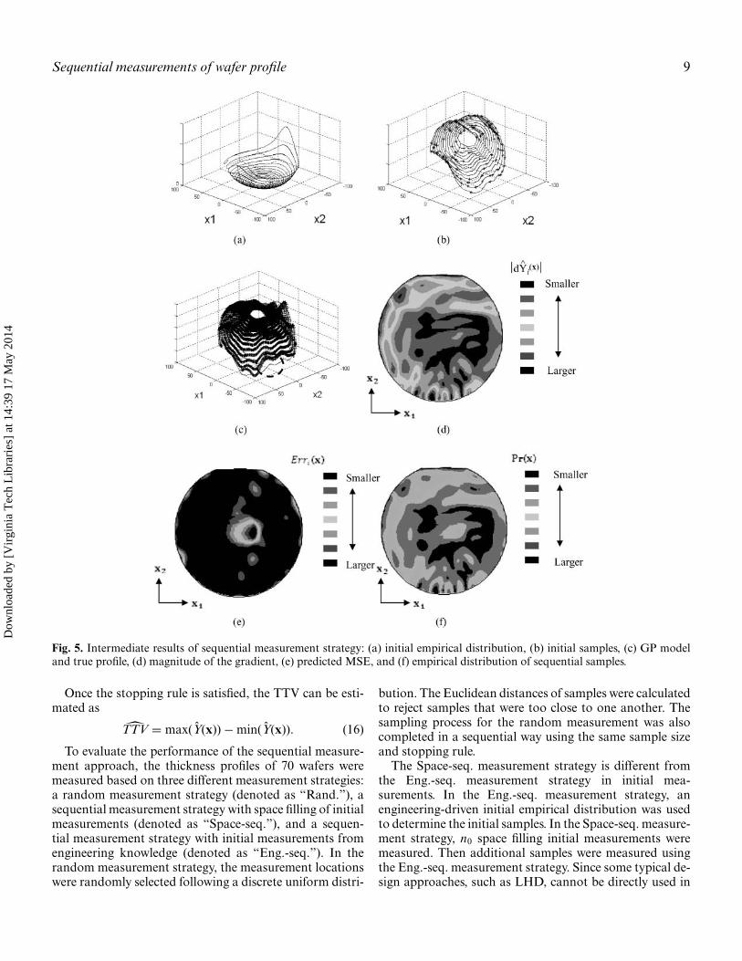
After the parameters were determined, a series of GPmodels was estimated and the samples were determined.Figure 5 shows the results obtained using the sequentialmeasurement procedure for thickness profile prediction.The initial sampling distribution was weighted by radiusand contact span, shown in Fig. 5(a). The initial sam-ples were measured to create an initial sample distributionof n0 = 100, and these locations are shown in Fig. 5(b),marked as stars. The measured data were then partionedinto a training sample set (75%) and a testing sample set
(25%). A GP model was estimated based on the trainingsample set (75 samples for the initial model fitting). In thismodel, the mean of the thickness profile was removed be-fore the modeling. Figure 5(c) shows a comparison of themeasured thickness profile (solid lines) and the estimatedprofile obtained using the GP model (“+” lines). The GPmodel was
Y(x) = −0.3011 + Z(x), (14)
where � = [5.95, 2.50], σ 2Z = 2.79, and RMSPEtest
0 is0.8662 µm. From Fig. 5(c), it can be seen that the GPmodel provides a close approximation of the overall waferprofile. However, a large prediction error can be observedat some locations (marked by a dashed circle), and at thesepoints the prediction is not accurate enough. Additionalsamples may be needed to further reduce these errors.
An additional 70 points were measured and the magni-tude of the gradient and predicted MSE for the additionalmeasurement could be estimated using the GP model inEquation (14), and the results are shown in Figs 5(d) and5(e), respectively. Finally, the empirical distribution for se-quential samples is shown in Fig. 5(f). A distance thresholdof 3 mm was used during the sampling of the data.
Once the additional samples were determined, all 170measured samples were again randomly partitioned into atraining sample set (75%) and a testing sample set (25%).The GP model was updated based on the training sampleset as
Y (x) = −0.4808 + Z (x) , (15)
where � = [4.20, 5.00], σ 2Z = 4.96, and RMSPEtest
0 is0.8389 µm. In this way, the GP model improves as thesample size increases.
The sequential samples were measured iteratively untilthe accuracy of the estimated quality variables satisfied thestopping rule. In this article, Thσ 2 = 0.04; i.e., the require-ment is a standard deviation of 0.2 µm. This accuracyrequirement is an engineering specification of the design inwafer manufacturing processes.
Dow
nloa
ded
by [
Vir
gini
a T
ech
Lib
rari
es]
at 1
4:39
17
May
201
4
Sequential measurements of wafer profile 9
Fig. 5. Intermediate results of sequential measurement strategy: (a) initial empirical distribution, (b) initial samples, (c) GP modeland true profile, (d) magnitude of the gradient, (e) predicted MSE, and (f) empirical distribution of sequential samples.
Once the stopping rule is satisfied, the TTV can be esti-mated as
TTV = max(Y(x)) − min(Y(x)). (16)
To evaluate the performance of the sequential measure-ment approach, the thickness profiles of 70 wafers weremeasured based on three different measurement strategies:a random measurement strategy (denoted as “Rand.”), asequential measurement strategy with space filling of initialmeasurements (denoted as “Space-seq.”), and a sequen-tial measurement strategy with initial measurements fromengineering knowledge (denoted as “Eng.-seq.”). In therandom measurement strategy, the measurement locationswere randomly selected following a discrete uniform distri-
bution. The Euclidean distances of samples were calculatedto reject samples that were too close to one another. Thesampling process for the random measurement was alsocompleted in a sequential way using the same sample sizeand stopping rule.
The Space-seq. measurement strategy is different fromthe Eng.-seq. measurement strategy in initial mea-surements. In the Eng.-seq. measurement strategy, anengineering-driven initial empirical distribution was usedto determine the initial samples. In the Space-seq. measure-ment strategy, n0 space filling initial measurements weremeasured. Then additional samples were measured usingthe Eng.-seq. measurement strategy. Since some typical de-sign approaches, such as LHD, cannot be directly used in
Dow
nloa
ded
by [
Vir
gini
a T
ech
Lib
rari
es]
at 1
4:39
17
May
201
4
10 Jin et al.
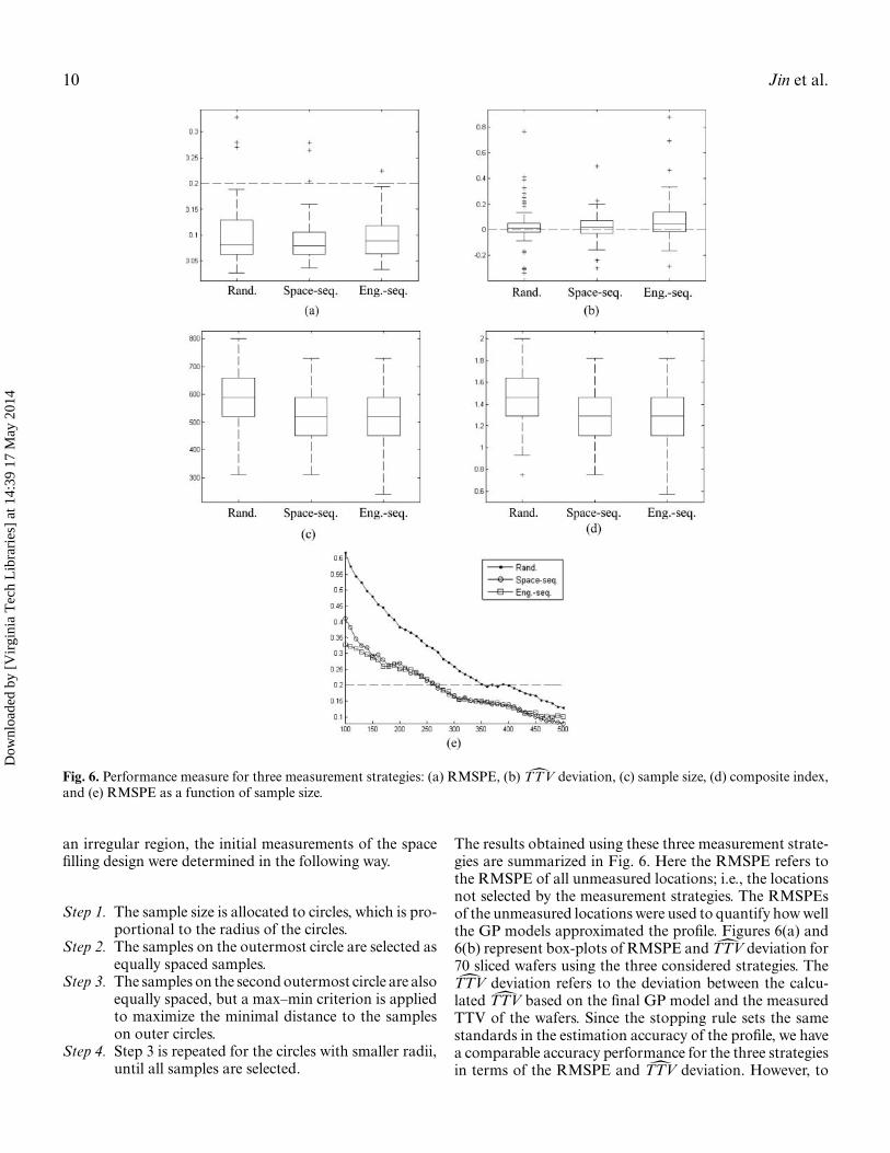
Fig. 6. Performance measure for three measurement strategies: (a) RMSPE, (b) TTV deviation, (c) sample size, (d) composite index,and (e) RMSPE as a function of sample size.
an irregular region, the initial measurements of the spacefilling design were determined in the following way.
Step 1. The sample size is allocated to circles, which is pro-portional to the radius of the circles.
Step 2. The samples on the outermost circle are selected asequally spaced samples.
Step 3. The samples on the second outermost circle are alsoequally spaced, but a max–min criterion is appliedto maximize the minimal distance to the sampleson outer circles.
Step 4. Step 3 is repeated for the circles with smaller radii,until all samples are selected.
The results obtained using these three measurement strate-gies are summarized in Fig. 6. Here the RMSPE refers tothe RMSPE of all unmeasured locations; i.e., the locationsnot selected by the measurement strategies. The RMSPEsof the unmeasured locations were used to quantify how wellthe GP models approximated the profile. Figures 6(a) and6(b) represent box-plots of RMSPE and TTV deviation for70 sliced wafers using the three considered strategies. TheTTV deviation refers to the deviation between the calcu-lated TTV based on the final GP model and the measuredTTV of the wafers. Since the stopping rule sets the samestandards in the estimation accuracy of the profile, we havea comparable accuracy performance for the three strategiesin terms of the RMSPE and TTV deviation. However, to
Dow
nloa
ded
by [
Vir
gini
a T
ech
Lib
rari
es]
at 1
4:39
17
May
201
4

Sequential measurements of wafer profile 11
achieve a comparable estimation accuracy of the profile,both the Space-seq. measurement strategy and Eng.-seq.measurement strategy use fewer samples, as shown in Fig.6(c), and they have smaller composite indexes, as shown inFig. 6(d).
The RMSPE values at different sample sizes are com-pared in Fig. 6(e). It is clear that the RMSPE values ofthe Space-seq. and Eng.-seq. measurement strategies havea better estimation performance than the random mea-surement strategy. The Eng.-seq. measurement strategy hasa better estimation performance when the sample size issmall, but it quickly converges to a similar performanceas that of the Space-seq. measurement strategy. This re-sult indicates that the initial empirical distribution providesuseful information to obtain a reliable initial GP modelfor sequential measurements. The sequential measurementstrategy performs well, even if engineering knowledge isnot available and the space filling initial measurements areused instead.
4. Conclusions
The geometric profiles of wafers are an important qualityfeature in semiconductor manufacturing. In most cases, themeasurements of the wafer profile are not available duringproduction, since it is time-consuming to measure profilesfor a large batch of wafers.
This article proposes an efficient sequential measurementstrategy to approximate the thickness profile by estimatedGP models. New empirical distributions are proposed todetermine measurement locations, including both the ini-tial distribution from engineering knowledge and the se-quential measurement distribution from the estimated GPmodels. In this article, the presented case study indicatesthat the proposed sequential measurement strategy requiresa smaller sample size to achieve a comparable estimationaccuracy to that of the random measurement strategy.Moreover, the initial empirical distribution allows a reli-able initial GP model to be obtained, when compared tothe space filling measurement strategy.
In the GP model estimation, the computation complex-ity is high when the training sample size becomes large,and the inversion of the covariance matrix may easily be-come ill-conditioned. In future research, computationallymore efficient metamodels will be studied to develop newmeasurement strategies.
Acknowledgement
The authors gratefully acknowledge the financial supportof the National Science Foundation under grant NSFCMMI-1030125.
References
Abburi, N.R. and Dixit, U.S. (2006) A knowledge-based system for theprediction of surface roughness in turning process. Robotics andComputer-Integrated Manufacturing, 22, 363–372.
Anderson, A.B., Wang, G. and Gertner, G. (2006) Local variability basedsampling for mapping a soil erosion cover factor by cosimulationwith Landsat TM images. International Journal of Remote Sensing,27, 2423–2447.
Atkinson, P.M., Webster, R. and Curran, P.J. (1992) Cokriging withground-based radiometry. Remote Sensing of Environment, 41, 45–60.
Atkinson, P.M., Webster, R. and Curran, P.J. (1994) Cokriging with air-borne MASS imagery. Remote Sensing of Environment, 50, 335–345.
Cohn, D.A. (1996) Neural network exploration using optimal experi-mental design. Neural Networks, 9, 1071–1083.
Curran, P.J. (1988) The semivariogram in remote sensing: an introduc-tion. Remote Sensing of Environment, 24, 493–507.
Curran, P.J. and Williamson, H.D. (1986) Sample size for ground andremotely sensed data. Remote Sensing of Environment, 20, 31–41.
Doucet, A., De Freitas, J.F.G. and Gordon, N. (2001) Sequential MonteCarlo in Practice, Cambridge University Press, Cambridge, UK.
Doucet, A., Godsill, S.J. and Andrieu, C. (2000) On sequential simulationbased methods for Bayesian filtering. Statistics and Computing, 10,197–208.
Forsey, D. and Bartels, R. (1988) Hierarchical B-spline refinement. Com-puter Graphics, 22, 205–212.
Gramacy, R.B. and Lee, H.K.H. (2009) Adaptive design and analysis ofsupercomputer experiment. Technometrics, 51, 130–145.
Guo, D. and Wang, X. (2004) Dynamic sensor collaboration via sequen-tial Monte Carlo. IEEE Journal on Selected Areas in Communica-tions, 22, 1037–1047.
Huang, D., Allen, T.T., Notz, W.I. and Miller, R.A. (2006) Sequentialkriging optimization using multiple-fidelity evaluations. Structureand Multidisciplinary Optimization, 32, 369–382.
Huang, X. and Gao, Y. (2010) A discrete system model for form errorcontrol in surface grinding. International Journal of Machine Toolsand Manufacture, 50, 219–230.
Kleijnen, J.P.C. and Van Beers, W.C.M. (2004) Application-driven se-quential designs for simulation experiments: kriging metamodelling.Journal of the Operational Research Society, 55, 876–883.
Lee, S., Wolberg, G. and Shin, S.Y. (1997) Scattered data interpolationwith multilevel B-splines. IEEE Transaction on Visualization andComputer Graphics, 3, 228–244.
Liu, J.S. and Chen, R. (1998) Sequential Monte Carlo methods for dy-namic systems. Journal of the American Statistical Association, 93,1032–1044.
Lophaven, S.N., Nielsen, H.B. and Søndergaard, J. (2002) Manual ofDACE. Available at http://www2.imm.dtu.dk/∼hbn/dace/.
Mackay, D.J.C. (1992) Information-based objective functions for activedata selection. Neural Computation, 4, 589-603.
McBratney, A.B. and Webster, R. (1983a) How many observations areneeded for regional estimation of soil properties? Journal of SoilScience, 135, 177–183.
McBratney, A.B. and Webster, R. (1983b) Optimal interpolation and is-arithmic mapping of soil properties V. Co-regionalization and mul-tiple sampling strategy. Journal of Soil Science, 34, 137–162.
Muller, P., Sanso, B. and De Iorio, M. (2004) Optimal Bayesian design byinhomogeneous Markov chain simulation. Journal of the AmericanStatistical Association, 99, 788–798.
Ozcelik, B. and Bayramoglu, M. (2006) The statistical modeling of sur-face roughness in high-speed flat end milling. International Journalof Machine Tools & Manufacture, 46, 1395–1402.
Park, S., Fowler, J.W., Mackulak, G.T., Keats, J.B. and Carlyle,W.M.M. (2002) D-optimal sequential experiments for generating a
Dow
nloa
ded
by [
Vir
gini
a T
ech
Lib
rari
es]
at 1
4:39
17
May
201
4

12 Jin et al.
simulation-based cycle time-throughput curve. Operations Research,50, 981–990.
Pei, Z.J., Kassir, S., Bhagavat, M. and Fisher, G.R. (2004) An experimen-tal investigation into soft-pad grinding of wire-sawn silicon wafers.International Journal of Machine Tools & Manufacture, 44, 299–306.
Pei, Z.J., Xin, X.J. and Liu, W. (2003) Finite element analysis for grindingof wire-sawn silicon wafers: a designed experiment. InternationalJournal of Machine Tools & Manufacture, 43, 7–16.
Santner, T.J., Williams, B.J. and Notz, W.I. (2003) The Design and Analysisof Computer Experiments, Springer, New York, NY.
Schonlau, M., Welch, W.J. and Jones, D.R. (1998) Global versus localsearch in constrained optimization of computer models. New Devel-opments and Applications in Experimental Design, 34, 11–25.
Schroder, P. (1996) Wavelets in computer graphics. Proceedings of theIEEE, 84, 615–625.
Sederberg, T.W., Cardon, D.L., Finnigan, G.T., North, N.S., Zheng, J.and Lyche, T. (2004) T-spline simplification and local refinement.ACM Transactions on Graphics, 3, 276–283.
Seo, S., Wallat, M., Graepel, T. and Obermayer, K. (2000) Gaussian pro-cess regression: active data selection and test point rejection, in Pro-ceedings of the International Joint Conference on Neural Networks,pp. 241–246.
Valette, S. and Prost, R. (2004) Wavelet-based multiresolution analysisof irregular surface meshes. IEEE Transaction on Visualization andComputer Graphics, 10, 113–122.
Wang, G., Gertner, Z.G. and Anderson, A.B. (2005) Sampling design anduncertainty based on spatial variability of spectral reflectance formapping vegetation cover. International Journal of Remote Sensing,26, 3255–3274.
Williams, B.J., Santner, T.J. and Notz, W.I. (2000) Sequential design ofcomputer experiments to minimize integrated response functions.Statistica Sinica, 10, 1133–1152.
Xiao, X., Gertner, G.Z., Wang, G. and Anderson, A.B. (2005) Optimalsampling scheme for estimation and landscape mapping of vegeta-tion cover. Landscape Ecology, 20, 375–387.
Zhang, G.M. and Kapoor, S.G. (1990) Dynamic generation of machinedsurfaces part 1: description of a random excitation system. Technicalreport. Institute for Systems Research, TR 1990-36.
Zhao, H., Jin, R. and Shi, J. (2011) PDE-constrained Gaussian processmodel on material removal rate of wiresaw slicing process mod-eling. ASME Transactions, Journal of Manufacturing Science andEngineering, 133(2), 021012-1–021012-9.
Zhu, L. and Kao, I. (2005) Galerkin-based modal analysis on the vibra-tion of wire–slurry system in wafer slicing using a wire saw. Journalof Sound and Vibration, 283, 589–620.
Biographies
Ran Jin is a Ph.D. student at the H. Milton Stewart School of Industrialand Systems Engineering at the Georgia Institute of Technology. Hereceived a B.Eng. in Electronics Information Engineering at TsinghuaUniversity, Beijing, in 2005, an M.S. in Industrial Engineering, and anM.A. in Statistics at the University of Michigan, Ann Arbor, in 2007 and2009, respectively. His research interests include data mining, engineeringknowledge–enhanced statistical modeling of complex systems, processmonitoring, diagnosis, and control.
Chia-Jung Chang is a Ph.D. student at the H. Milton Stewart School ofIndustrial and Systems Engineering, Georgia Institute of Technology. Shereceived both her B.S. and M.S. degrees from the Industrial Engineeringand Engineering Management Department at National Tsing-Hua Uni-versity in Taiwan in 2005 and 2007, respectively. Her research interestsfocus on quality engineering and applied statistics, system informaticsand control of complex systems, and design of experiments.
Jianjun Shi is the Carolyn J. Stewart Chair Professor at the H. MiltonStewart School of Industrial and Systems Engineering, Georgia Insti-tute of Technology. Before joined Georgia Tech in 2008, he was the G.Lawton and Louise G. Johnson Professor of Engineering at the Univer-sity of Michigan. He was awarded B.S. and M.S. degrees in ElectricalEngineering at the Beijing Institute of Technology in 1984 and 1987, re-spectively, and a Ph.D. in Mechanical Engineering at the University ofMichigan in 1992. His research interests focus on the fusion of advancedstatistics, signal processing, control theory, and domain knowledge to de-velop methodologies for modeling, monitoring, diagnosis, and control ofcomplex systems in data-rich environments. He is the founding chairper-son of the Quality, Statistics and Reliability subdivision at INFORMS.He currently serves as the Focus Issue Editor of IIE Transactions onQuality and Reliability Engineering. He is a Fellow of the Institute ofIndustrial Engineering, a Fellow of the American Society of Mechani-cal Engineering, a Fellow of the Institute of Operations Research andManagement Science, and also a life member of ASA.
Dow
nloa
ded
by [
Vir
gini
a T
ech
Lib
rari
es]
at 1
4:39
17
May
201
4