GLOBAL Fulong Wu, Bartlett Professor of Planning UCL, UK ...
Massively Parallel Optical Manipulation of Single Cells, Micro- and Nano-particles on Optoelectronic Devices
by
Pei-Yu Chiou
B.S. (National Taiwan University) 1998 M.S. (University of California at Los Angeles) 2004
A dissertation submitted in partial satisfaction of the
requirement for the degree of
Doctor of Philosophy
in
Engineering-Electrical Engineering and Computer Sciences
in the
GRADUATION DIVISION
of the
UNIVERSITY OF CALIFORNIA AT BERKELEY
Committee in charge:
Professor Ming C. Wu, chair Professor Connie J. Chang-Hasnain
Professor Luke P. Lee
Fall 2005
The dissertation of Pei-Yu Chiou is approved:
__________________________________________________________ Professor Ming C. Wu, Chair Date
__________________________________________________________ Professor Connie J. Chang-Hasnain Date
__________________________________________________________ Professor Luke P. Lee Date
University of California, Berkeley
Fall 2005
Massively Parallel Optical Manipulation of Single Cells, Micro- and Nano-particles on Optoelectronic Devices
Copyright © 2005
by
Pei-Yu Chiou
1
Abstract
Massively Parallel Optical Manipulation of Single Cells, Micro- and Nano-particles on Optoelectronic Devices
by
Pei-Yu Chiou
Doctor of Philosophy in Electrical Engineering and Computer Sciences
University of California, Berkeley
Professor Ming C. Wu, chair
The ability to manipulate biological cells and micrometer-scale particles plays an
important role in many biological and colloidal science applications. However,
conventional manipulation techniques, such as optical tweezers, electrokinetic forces
(electrophoresis, dielectrophoresis (DEP), and traveling-wave dielectrophoresis),
magnetic tweezers, acoustic traps, and hydrodynamic flows, cannot achieve high
resolution and high throughput at the same time. Optical tweezers offers high resolution
for trapping single particles, but has a limited manipulation area due to tight focusing
requirements, while electrokinetic forces and other mechanisms provide high throughput,
but lack the flexibility or the spatial resolution necessary for controlling individual
particles.
In the dissertation, I present a novel concept called optoelectronic tweezers (OET).
Using light-driven electrokinetic mechanisms (dielectrophoresis, ac electroosmosis),
OET permits high-resolution patterning of electric fields on a photoconductive surface
for manipulating single cells, micro- and nano-particles with light intensity of 10 nW/cm2,
2
which is 100,000 times less than with optical tweezers. It opens up the possibility of
optical manipulation using an incoherent light source such as light emitting diode (LED)
or a halogen lamp. Integrating with a digital micromirror or a liquid crystal spatial light
modulator, we have demonstrated parallel manipulation of 31,000 particle traps on a
1.3×1.0 mm2 area. Using OET technique, we have demonstrated optical manipulation on
various polystyrene particles with size range from 45 µm to 500 nm, bacteria (E. Coli),
cancer cells (HeLa), and human white blood and red blood cells. With direct optical
imaging control, multiple manipulation functions can be combined to achieve complex,
multi-step manipulation protocols.
_______________________________________________
Professor Ming C. Wu, Chair Date

i
To my parent
ii
TABLE OF CONTENTS
Chapter 1
Introduction
1.1. Introduction of Tools for Cell, Micro- and Nano-Particle Manipulation 1
1.2. Dielectrophoresis (DEP) 6
1.2.1 CM Factor of Multi-Layer Particles 7
1.2.2 Effect of Surface Conductance on Nanoparticles 11
1.3. Electroosmosis 13
1.3.1 Electric Double Layer 13
1.3.2 Electroosmosis 17
1.3.3 AC electroosmosis 20
1.4. Reference 21
Chapter 2
Principle of Optoelectronic Tweezers (OET)
2.1. Introduction 26
2.2. Amorphous silicon as a photosensitive material 29
2.3. OET Device Design 32
2.4. OET Device Fabrication 34
2.5. Simulated Electric Field Distribution 35
2.6. OET Manipulation of Polystyrene Beads 42
2.7. OET Trapping of Live Bacteria (E. Coli) 47
2.8. AC Frequency Range for OET Operation 56
2.9. Photocurrent Measurement and Simulation of OET 59
2.10. Reference 70
Chapter 3
Scanning OET for Microparticle Sorting
iii
3.1 Introduction 72
3.2 Sorting Mechanism 72
3.3 Experimental Setup and Results 75
3.4 Reference 78
Chapter 4
Optical Image Driven OET for Massively Parallel Manipulation
4.1. Introduction 80
4.2. System of Direct Optical Image Driven OET using a LED 81
4.3. Virtual Particle Concentrator and Conveyer 82
4.4. Selective Concentration of Live White Blood Cells 84
4.5. Massively Parallel Optical Manipulation of Microscopic Particles 85
4.6. Integrated Dynamic Optical Patterns for Multi-Step Manipulation 88
4.7. Long-Term Photodegradation of Photoconductivity in Amorphous Silicon 91
4.8. Reference 92
Chapter 5
Image Feedback Controlled OET for Automatic Processing
5.1. Introduction 94
5.2. Microvision-Activated OET system 94
5.3. Particle Recognition Process 96
5.4. Automatic Generation of Optical Patterns for Functional Manipulation 100
5.5. Continuous Sorting of Particles and Cells Based on Size and Color 104
5.6. Reference 114
Chapter 6
Light-patterned AC Electroosmosis for Nanoparticle Manipulation
6.1. Introduction 115
6.2. Analytical Model of Llight-Patterned AC Electroosmotic Flow 116
6.3. Numerical Simulation of Light-Patterned AC Electroosmotic Flow 123

iv
6.4. Light-Patterned AC Electroosmosis for Nanoparticle Trapping 130
6.5. Reference 135
Chapter 7
Conclusion 136

v
Acknowledgement
I would like to thank Prof. Ming C. Wu for his mentoring in the past five years.
My research would not be as fruitful as what has been included in this dissertation
without his continuous encouraging and supporting in the difficult time during the
process. I would also like to thank Prof. Chih-Ming Ho (in UCLA MAE department) and
the CMISE center for giving me so much multi-discipline training experience and
exposure to researchers from other fields. This provided me a much broader view of the
research environment and inspired many novel ideas in my mind than I could expect. I
would also like to thank Prof. Connie Chang Hasnian for her kindness of being my
qualify committee chair and also the committee of my dissertation. I would also like to
thank Prof. Luke Lee for being my committee in my qualify exam and dissertation. His
positive feedback to my research is my biggest reward as a Ph.D student.
In the past five years, I have received numerous help from my labmates in IPL. I
would like to give my special thanks to Aaron T. Ohta for his great help in both research
and English writing.
As an engineering student who is new to biological field, my dear friend Yu-
Ching (Kelly) Yang has being my greatest help in bridging the knowledge between the
biological and engineering fields. She is my tutor in biology in research and my mental
companion in life.
Finally, I would like to thank my parent for their support for my study so far away
from home.
1
CHAPTER 1
INTRODUCTION
1.1. Introduction of Tools for Cell, Micro- and Nano-Particle
Manipulation
Tools for manipulating small particles such as cells, micro-particles and nano-
particles play important roles in the fields of biological research and colloid science.
These tools are used to perform important functions such as the sorting, addressing,
transporting, and trapping of cells and particles in these fields. Several mechanisms have
been applied to manipulate small particles are versatile, including optical tweezers [1],
electrophoresis [2], dielectrophoresis [3], magnetic tweezers [4], acoustic force [5], and
hydrodynamic force [6]. Each technique has its advantages and unique features. For
example, optical tweezers provides precise trapping of single particles, but the number of
particles that can be manipulated in parallel is limited. Electrokinetic mechanisms
(electrophoresis and dielectrophoreisis) can achieve high throughput, but control at the
single-cell or single-particle level is limited. The same is true for other mechanisms such
as magnetic tweezers, or hydrodynamic forces. The restriction comes from the limitation
of addressing these forces to individual cells without interference with each other. Tools
that can simultaneously achieve high resolution and high throughput are missing.
2
Optical tweezers was first proposed by Ashkin in 1986[7]. It has become a
powerful tool in biological fields for trapping cells and characterizing the forces of bio-
molecules and molecular motors. The optical force originates from the transfer of the
photon momentum from the incident light beam to the manipulated particle. The first
optical radiation force was observed by Ashkin in 1970, showing that a focused laser
beam can affect the dynamics of small transparent particles[8]. Two forces were
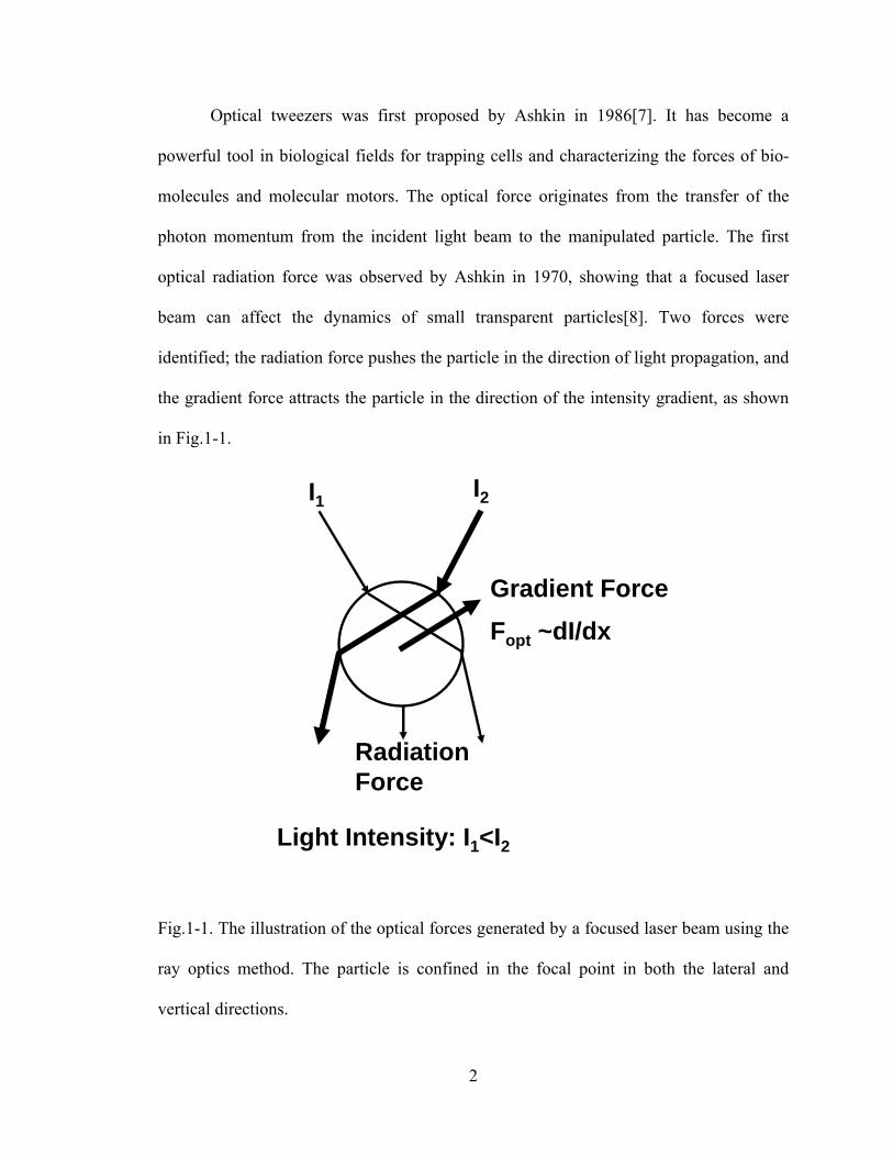
identified; the radiation force pushes the particle in the direction of light propagation, and
the gradient force attracts the particle in the direction of the intensity gradient, as shown
in Fig.1-1.
Fopt ~dI/dx
RadiationForce
Gradient Force
I2I1
Light Intensity: I1<I2
Fig.1-1. The illustration of the optical forces generated by a focused laser beam using the
ray optics method. The particle is confined in the focal point in both the lateral and
vertical directions.
3
To form a stable particle trap in the focal point, the gradient force needs to
overcome the scattering force that pushes the particle out of the trap point. An objective
lens with high numerical aperture (typically N.A. > 1) is required to form a tightly
focused laser beam in which the gradient force dominates at the focal point [1]. The first
single beam optical tweezers was demonstrated in 1986, with the trapping of a
submicron silica sphere using a highly focused 514 nm argon laser [7]. For biological cell
manipulation, a tightly focused laser beam with wavelength at the near infrared window
is used to prevent optical damage to the cell due to the heat generated from absorption of
the strong incident laser beam [9, 10]. The force generated by optical tweezers can be up
to the nanonewton level, depending on the optical power and the efficiency of the optical
trap. The force of the optical trap can be expressed by c
nPQF = , where c/n is the speed
of light in the medium, P is the optical power and Q is the trap efficiency[11]. For a
spherical particle with a radius equal to the wavelength of light, the efficiency is ~ 0.1
and the optical force is ~ 0.5 pN/mW. For particles much smaller than the wavelength,
the efficiency decreases as the optical force in this size range is proportional to the
volume of the particles.
However, optical tweezers has some limitations. The effective manipulation area
is limited by the field of view of the high N.A. objective lens. For a 100× oil immersion
lens, the effective area is less than 100 × 100 µm2, limiting the capability of parallel
manipulation to a small number of cells (the size of a mammalian cell is ~ 10 µm).
Increasing the manipulation area by using a low N.A. objective lens is possible, but
sacrifices the strength of the gradient force, resulting in a less stable trap. A further
limitation is the high light intensity requirement for optical traps. The minimum optical
4
power required to overcome the Brownian motion of the trapped particle, forming a
stable optical trap, is ~ 1 mW [12]. The power required for multiple traps is proportional
to the number of traps. To operate a typical holographic optical tweezers setup, a high-
power laser with 200 mW to 4W output power is required [12, 13]. The maximum laser
power is limited by the photodamage threshold of light-sensitive components such as the
spatial light modulator.
Magnetic forces are frequently used for the sorting of biological cells because
magnetic fields have less effects on the manipulated cells than electrical or optical fields.
Magnetic beads are polymer spheres containing a large number of superparamagnetic
nanoparticles. The surface of the magnetic bead can be functionalized with antibodies,
peptides, or lectins, to attach to or be engulfed by cells [14-16]. The target cells
recognized by these biomarkers are attached by the magnetic beads and can be sorted out
by applying a magnetic field. To achieve high-resolution manipulation using a magnetic
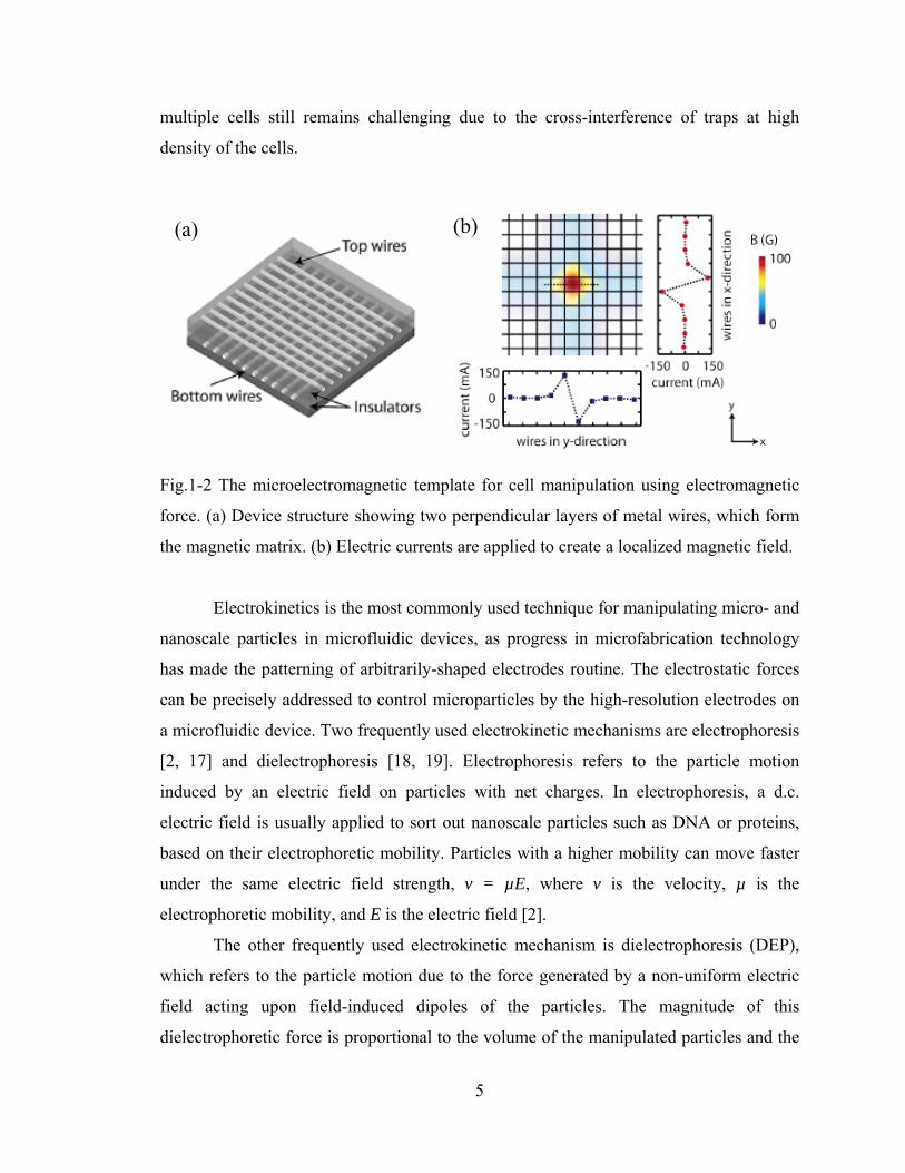
field, a microelectromagnetic template has been proposed to manipulate single cells as
shown in Fig.1-2 [4]. By controlling the applied electric currents to the programmed
wires in the matrix, a highly localized magnetic field profile can be created to address the
cells that have been pretreated with functionalized magnetic beads. The force generated
in the magnetic field can be expressed as BmF ∇⋅= , where m is the magnetic moment
and B is the magnetic flux. Due to the supermagnetic nature of the beads, the magnetic
moment is proportional to the field, m=VχB/µo, where V is the volume of the magnetic
bead, χ is the susceptibility of the bead, and µo is the permeability in the vacuum [4]. The
magnetic trap force is 2
21 BVF
o
∇= χμ
. For the applied current shown in Fig.1-2(b), a
peak magnetic flux of 10 mT and a maximum magnetic force of 40 pN are created.
There are, however, some limitations of using magnetic tweezers. The attachment
of magnetic beads to cells may affect the cells’ intrinsic properties, which may prevent
the user from observing the original cell responses. Although the microelectromagnetic
template has shown the potential to manipulate single cells, parallel manipulation of
5
multiple cells still remains challenging due to the cross-interference of traps at high
density of the cells.
Fig.1-2 The microelectromagnetic template for cell manipulation using electromagnetic
force. (a) Device structure showing two perpendicular layers of metal wires, which form
the magnetic matrix. (b) Electric currents are applied to create a localized magnetic field.
Electrokinetics is the most commonly used technique for manipulating micro- and
nanoscale particles in microfluidic devices, as progress in microfabrication technology
has made the patterning of arbitrarily-shaped electrodes routine. The electrostatic forces
can be precisely addressed to control microparticles by the high-resolution electrodes on
a microfluidic device. Two frequently used electrokinetic mechanisms are electrophoresis
[2, 17] and dielectrophoresis [18, 19]. Electrophoresis refers to the particle motion
induced by an electric field on particles with net charges. In electrophoresis, a d.c.
electric field is usually applied to sort out nanoscale particles such as DNA or proteins,
based on their electrophoretic mobility. Particles with a higher mobility can move faster
under the same electric field strength, v = µE, where v is the velocity, µ is the
electrophoretic mobility, and E is the electric field [2].
The other frequently used electrokinetic mechanism is dielectrophoresis (DEP),
which refers to the particle motion due to the force generated by a non-uniform electric
field acting upon field-induced dipoles of the particles. The magnitude of this
dielectrophoretic force is proportional to the volume of the manipulated particles and the
(b)(b)(a)
6
gradient of the electric field intensity (E2). Dielectrophoresis has been used to trap and
sort micro- and nano-meter particles such as cells, bacteria, and viruses [18, 20-23].
Electrokinetic mechanisms are convenient tools for cell manipulation in multi-
particle or batch modes. However, to manipulate single cells that are randomly
distributed on a surface, it needs high-resolution, pre-patterned electrode pixels to address
single cells. The chip also needs to cover sufficiently large areas to allow dispersion of
single cells. The wiring and addressing of these electrodes becomes one of the challenges
of using electrokinetic mechanisms for single cell manipulation. To solve this issue, a
complementary metal oxide semiconductor (CMOS) DEP has been proposed for parallel
manipulation of more than 10,000 electrodes[24]. However, the CMOS DEP chip might
be cost effective for many biological applications, especially for disposable devices for
the prevention of cross-contamination.
To summarize, optical tweezers offers high resolution for trapping single particles,
but has a limited manipulation area due to tight focusing requirements, while
electrokinetic forces and other mechanisms provide high throughput, but lack the
flexibility or the spatial resolution necessary for controlling individual cells. In this
dissertation, I propose optical image-driven electrokinetic mechanisms for massively
parallel real-time manipulation of single cells, micro- and nano-particles in real-time on
optoelectronic devices. This novel mechanism permits optical manipulation with a light
intensity 100,000 times less than optical tweezers and dramatically increases the effective
manipulation area for parallel manipulation using light. The light-driven electrokinetic
mechanisms also avoid the wiring issues present in addressing electrokinetic mechanisms
using patterned electrodes, promising the parallel manipulation of single cells on a low
cost, disposable, silicon-coated glass slide. Details of the applied electrokinetic
mechanisms are discussed in the following sessions.
1.2. Dielectrophoresis (DEP) Dielectrophoresis refers to the motion of a particle induced by the interaction
between a non-uniform electric field and the induced electric dipole of the particle. The
magnitude of DEP force can be expressed as [25]
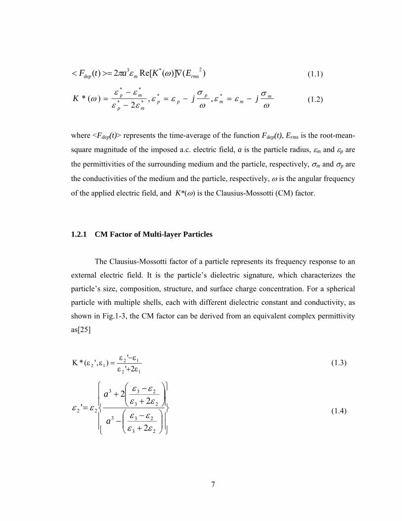
7
)()](Re[2)( 2*3rmsmdep EKatF ∇>=< ωεπ (1.1)
ωσεε
ωσ
εεεεεε
ω mmm
ppp
mp
mp jjK −=−=−
−= **
**
**
,,2
)(* (1.2)
where <Fdep(t)> represents the time-average of the function Fdep(t), Erms is the root-mean-
square magnitude of the imposed a.c. electric field, a is the particle radius, εm and εp are
the permittivities of the surrounding medium and the particle, respectively, σm and σp are
the conductivities of the medium and the particle, respectively, ω is the angular frequency
of the applied electric field, and K*(ω) is the Clausius-Mossotti (CM) factor.
1.2.1 CM Factor of Multi-layer Particles
The Clausius-Mossotti factor of a particle represents its frequency response to an
external electric field. It is the particle’s dielectric signature, which characterizes the
particle’s size, composition, structure, and surface charge concentration. For a spherical
particle with multiple shells, each with different dielectric constant and conductivity, as
shown in Fig.1-3, the CM factor can be derived from an equivalent complex permittivity
as[25]
12
1212 2'
'),'(*Kε+εε−ε
=εε (1.3)
⎪⎪⎭
⎪⎪⎬
⎫
⎪⎪⎩
⎪⎪⎨
⎧
⎟⎟⎠
⎞⎜⎜⎝
⎛+−
−
⎟⎟⎠
⎞⎜⎜⎝
⎛+−
+=
23
233
23
233
22
2
22
'
εεεεεεεε
εεa
a
(1.4)
8
R1
R2
R1
ε2ε3 ε2’
ε1: Medium
Fig.1-3 Spherical dielectric shells with radii of R1 and R2 and shell permittivities of ε2
and ε3, respectively.
where ε1, ε2, ε3 are the complex permittivities of the medium and the shells of the particle,
a=R1/R2, and ε2’ is the new equivalent permittivity of the particle. The real part of K*(ω),
Re[K*(ω)], has a value between 1 and –1/2, depending on the polarizability of the
medium and the particle at a certain frequency. If Re[K*(ω)] >0, the induced electric
dipole is collinear with the electric field as shown in Fig.1-4(a). The particle will move
towards the strong electric field region, a phenomenon known as positive DEP. On the
other hand, if Re[K*(ω)] <0, the induced electric dipole is anti-parallel to the electric
field as shown in Fig.1-4(b). The particle moves towards the weaker electric field region,
known as negative DEP.
9
Positive DEP Negative DEPPositive DEP Negative DEP
Fig.1-4 Illustration of positive and negative DEP forces. (a) For positive DEP, the field
induced electric dipole on the particle is collinear with the direction of the applied electric
field. The particles move towards the strong electric field region. (b) For negative DEP,
the dipole direction is anti-parallel to the applied electric field and the particles are
pushed towards the weaker electric field region.
104 105 106 107 108-1.0-0.8-0.6-0.4-0.20.00.20.40.60.81.0
Re(
K(f)
)
Electric Field Frequency (Hz)
1S/m
0.1S/m
0.001S/m
0.01S/m
104 105 106 107 108-1.0-0.8-0.6-0.4-0.20.00.20.40.60.81.0
Re(
K(f)
)
Electric Field Frequency (Hz)
1S/m
0.1S/m
0.001S/m
0.01S/m σ=0.5s/mε=80
σ=10-8 s/mε=10
D=10 µm
Cell Membrane: 10 nm
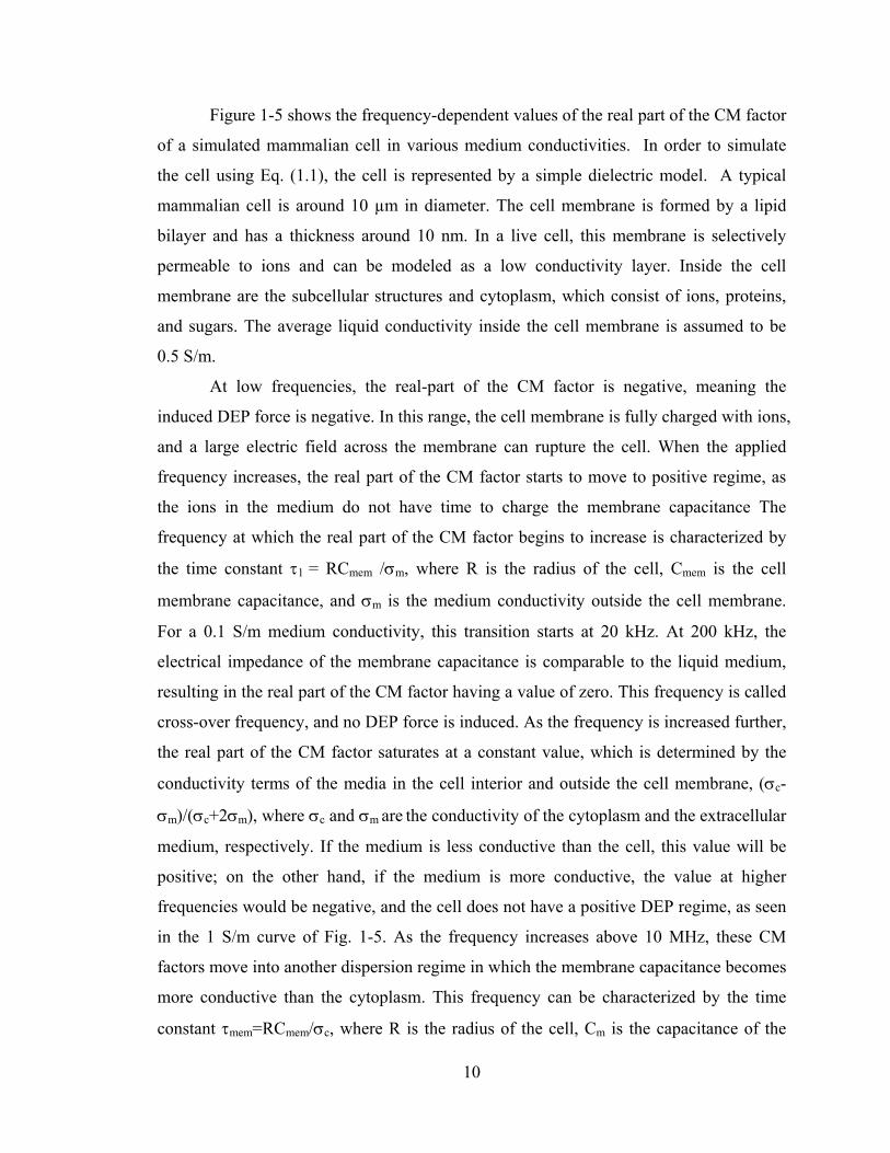
Fig.1-5 The simulated real part CM factor of a 10-µm mammalian cell in mediums with
liquid conductivities of 1 mS/m, 10 mS/m, 100 mS/m, and 1 S/m. The cell membrane is
assumed to have a 10 nm thickness and a low conductivity. Inside the cell membrane, the
liquid conductivity is assumed to have a constant value of 0.5 S/m.
10
Figure 1-5 shows the frequency-dependent values of the real part of the CM factor
of a simulated mammalian cell in various medium conductivities. In order to simulate
the cell using Eq. (1.1), the cell is represented by a simple dielectric model. A typical
mammalian cell is around 10 µm in diameter. The cell membrane is formed by a lipid
bilayer and has a thickness around 10 nm. In a live cell, this membrane is selectively
permeable to ions and can be modeled as a low conductivity layer. Inside the cell
membrane are the subcellular structures and cytoplasm, which consist of ions, proteins,
and sugars. The average liquid conductivity inside the cell membrane is assumed to be
0.5 S/m.
At low frequencies, the real-part of the CM factor is negative, meaning the
induced DEP force is negative. In this range, the cell membrane is fully charged with ions,
and a large electric field across the membrane can rupture the cell. When the applied
frequency increases, the real part of the CM factor starts to move to positive regime, as
the ions in the medium do not have time to charge the membrane capacitance The
frequency at which the real part of the CM factor begins to increase is characterized by
the time constant τ1 = RCmem /σm, where R is the radius of the cell, Cmem is the cell
membrane capacitance, and σm is the medium conductivity outside the cell membrane.
For a 0.1 S/m medium conductivity, this transition starts at 20 kHz. At 200 kHz, the
electrical impedance of the membrane capacitance is comparable to the liquid medium,
resulting in the real part of the CM factor having a value of zero. This frequency is called
cross-over frequency, and no DEP force is induced. As the frequency is increased further,
the real part of the CM factor saturates at a constant value, which is determined by the
conductivity terms of the media in the cell interior and outside the cell membrane, (σc-
σm)/(σc+2σm), where σc and σm are the conductivity of the cytoplasm and the extracellular
medium, respectively. If the medium is less conductive than the cell, this value will be
positive; on the other hand, if the medium is more conductive, the value at higher
frequencies would be negative, and the cell does not have a positive DEP regime, as seen
in the 1 S/m curve of Fig. 1-5. As the frequency increases above 10 MHz, these CM
factors move into another dispersion regime in which the membrane capacitance becomes
more conductive than the cytoplasm. This frequency can be characterized by the time
constant τmem=RCmem/σc, where R is the radius of the cell, Cm is the capacitance of the
11
cell membrane, and σc is the conductivity of the cytoplasm. The time constant τmem is cell
size-dependent and is equal to 8.8×10⁻⁸ sec for a 10-µm cell. Another time constant, τm =
εm/σm also plays an important role at this frequency range. For a 0.01 S/m aqueous
medium, τm has a value of 7×10⁻⁸ sec. When the applied frequency is higher than
f=1/(2πτm), the medium conductivity is dominated by the dielectric term, which increases
with the frequency [25]. This results in the decrease of the positive CM factors at
frequencies above 10 MHz for media with conductivities of 0.001 S/m, 0.01 S/m, and 0.1
S/m(Fig.1-5).
This multi-layer model can also predict the frequency-dependent CM factor for
bacteria, by adding one more layer to account for the cell wall (if necessary).
1.2.2 Effect of Surface Conductance on Nanoparticles
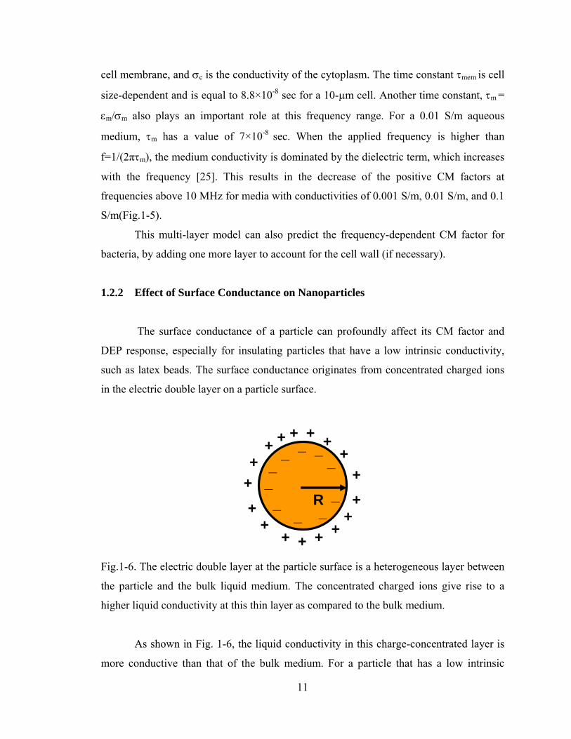
The surface conductance of a particle can profoundly affect its CM factor and
DEP response, especially for insulating particles that have a low intrinsic conductivity,
such as latex beads. The surface conductance originates from concentrated charged ions
in the electric double layer on a particle surface.
+ ++
++
+++++
++++
++
+R
__
__
_
_ __
__
Fig.1-6. The electric double layer at the particle surface is a heterogeneous layer between
the particle and the bulk liquid medium. The concentrated charged ions give rise to a
higher liquid conductivity at this thin layer as compared to the bulk medium.
As shown in Fig. 1-6, the liquid conductivity in this charge-concentrated layer is
more conductive than that of the bulk medium. For a particle that has a low intrinsic
12
conductivity, the overall particle conductivity is dominated by the surface conductance,
resulting in a frequency-dependent CM factor that is similar to that of a conductive
particle. The new effective particle conductivity, modified by the surface conductance,
can be expressed as [26]
Rpρμσσ 2
int += (1.5)
where σp, σint, ρ, µ, R are the particle’s effective conductivity, particle’s intrinsic
conductivity, surface charge density, ion mobility, and the radius of the particle,
respectively. Nanoscopic particles are more sensitive to the surface conductance than the
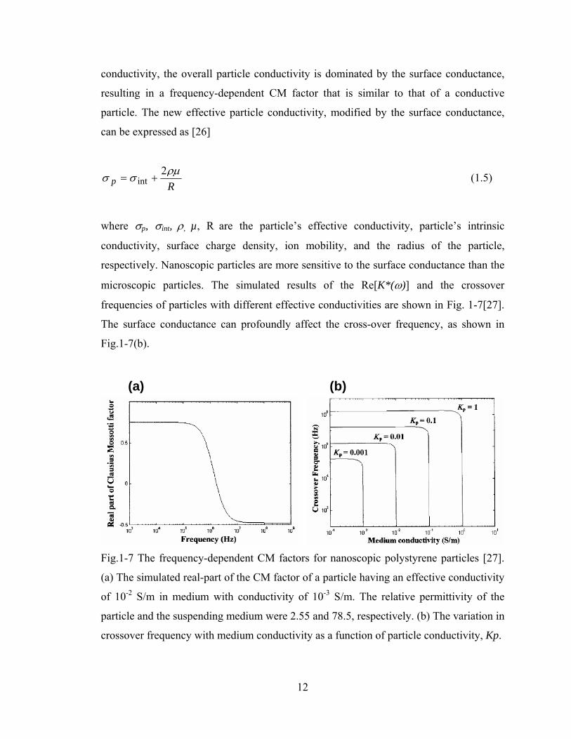
microscopic particles. The simulated results of the Re[K*(ω)] and the crossover
frequencies of particles with different effective conductivities are shown in Fig. 1-7[27].
The surface conductance can profoundly affect the cross-over frequency, as shown in
Fig.1-7(b).
(a) (b)
Fig.1-7 The frequency-dependent CM factors for nanoscopic polystyrene particles [27].
(a) The simulated real-part of the CM factor of a particle having an effective conductivity
of 10-2 S/m in medium with conductivity of 10-3 S/m. The relative permittivity of the
particle and the suspending medium were 2.55 and 78.5, respectively. (b) The variation in
crossover frequency with medium conductivity as a function of particle conductivity, Kp.
13
1.3. Electroosmosis
1.3.1 Electric Double Layer
In an electrochemical system where no charge can be transferred across the
electrode-solution interface, the electrode is called an ideal polarized electrode. The
electrode-solution interface behaves as a capacitor. As a potential is applied to the
electrode, charges will start to accumulate in the capacitor until the potential drop across
the capacitor is equal to the applied potential. During the charging process, charging
current is induced in the liquid, whose magnitude is limited by the resistance of the bulk
liquid medium. The charge on the metal, qm, represents the excess or deficiency of
electrons accumulating in a very thin layer (< 0.01 nm) on the metal surface. The charge
in the solution, qS, is made up of an excess of cations or anions in the vicinity of the
electrode surface. The whole array of charged species existing at the metal-solution
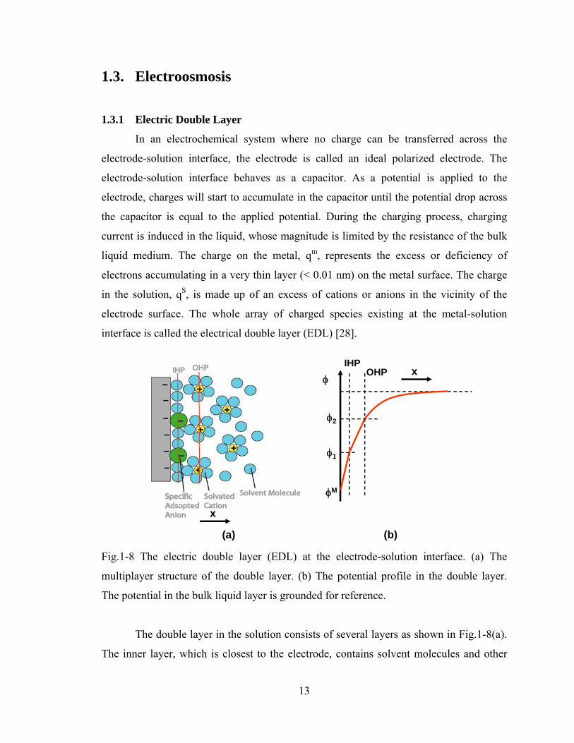
interface is called the electrical double layer (EDL) [28].
x
x
IHPOHP
φ
φM
φ1
φ2
(a) (b) Fig.1-8 The electric double layer (EDL) at the electrode-solution interface. (a) The
multiplayer structure of the double layer. (b) The potential profile in the double layer.
The potential in the bulk liquid layer is grounded for reference.
The double layer in the solution consists of several layers as shown in Fig.1-8(a).
The inner layer, which is closest to the electrode, contains solvent molecules and other
14
species that are specifically absorbed. This layer is also called the compact, Helmholtz, or
Stern layer. The locus of the electrical charge centers of the specifically absorbed ions is
called the inner Helmholtz plane (IHP). The solvated ions can only approach the
electrode at a distance beyond the IHP. The locus of the electrical centers of the closest
solvated ions is called the outer Helmholtz plane (OHP). The solvated ions and the
electrode interact via only long-range electrostatic forces, which is independent of the
chemical properties of the ions. The solvated ions are nonspecifically absorbed. Due to
thermal agitation, these ions extend from the OHP to the bulk solution, and form a three-
dimensional region called the diffuse layer. In equilibrium, the sum of the total charges of
the specifically absorbed ions and the nonspecifically absorbed ions is equal to that of the
charges on the electrode.
Even though the charge on the electrode is confined to the surface, it may take a
significant distance to accumulate enough ions in the diffuse double layer to
counterbalance the charges on the electrode, especially in solutions with a low electrolyte
concentration. The highest concentration of excess charges is adjacent to the electrode, as
there is a strong electrostatic force attracting these ions. The ion concentration becomes
progressively less at longer distances, since the electric field is partially screened by the
ions that are accumulated closer to the electrode. Gouy and Chapman have offered a
statistical mechanics approach to describe the relation between the applied potential and
the ion distribution in the diffuse double layer. In their approach, the Poisson equation in
electrostatic and the Boltzmann distribution in statistical mechanics are coupled to yield
the Poisson-Boltzmann equation to describe the system[29, 30]:
∑ −−=
i
ii
oi
o kTez
znedxd )exp(2
2 φεε
φ (1.6)
where φ is the potential measured with respect to the bulk solution, e is the electron
charge, nio is the bulk concentration of ion i, zi is the number of the valence electrons of
ion I ( for example, the valence of K+ is 1), k is the Boltzmann constant, and T is the
temperature. At the electrode surface, x=0. Solving Eq.(1.6) generates a potential profile
expressed as
15
xekToze
kTze κφφ −=
)4/tanh()4/tanh( (1.7)
where 2/1)222(
kTo
ezonkεε
= (1.8)
and φo is the potential at x=0, relative to the bulk solution. The value 1/κ is defined as the
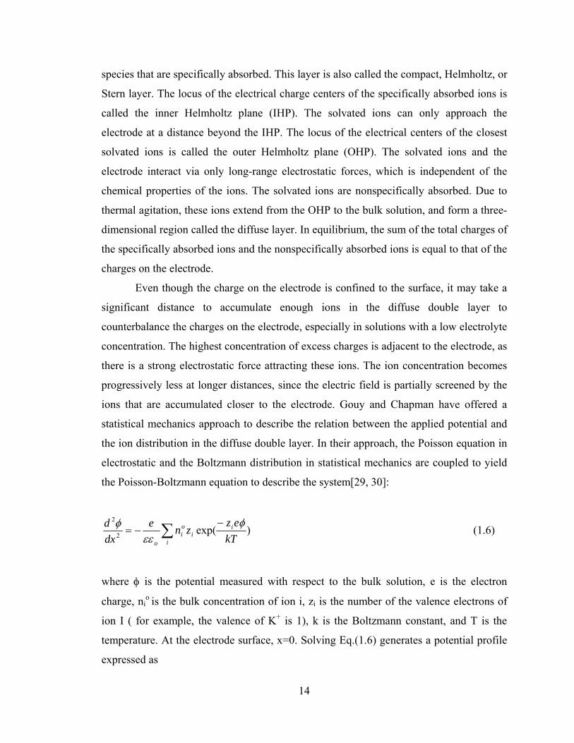
thickness of the diffuse layer, which depends on the electrolyte concentration. The diffuse
layer thickness in the high-concentration solutions is shorter than that of low-
concentration solutions. The diffuse layer is as thick as 30 nm in a solution with an
electrolyte concentration of 10-4M. In a typical bio-buffer (a buffer solution for biological
cells), the electrolyte concentration is ~ 100 mM, resulting in a double layer thickness of
~ 1 nm. Fig.1-9 shows the diffuse layer thickness as calculated from Eq.(1.8).
Dou
ble
Laye
r Thi
ckne
ss (m
)
Fig.1-9 The thickness of the diffuse layer calculated from Eq.(1.8).
The charge density at the electrode surface, σM, or the charge in the double layer,
σS, can be derived from Eq.(1.7) using Gauss’s Law:
16
∫ ⋅= surface dSEoq εε (1.9)
∫=
⎟⎠⎞
⎜⎝⎛= surface dS
xdxd
oq0
φεε (1.10)
)2
sinh(2/1)8(kT
ozeonokTSM φεεσσ =−= (1.11)
By differentiating Eq. (1.11), the differential capacitance is calculated:
)2
cosh(2
2/122
kTze
kTnez
C oo
od
φεε⎟⎟⎠
⎞⎜⎜⎝
⎛= (1.12)
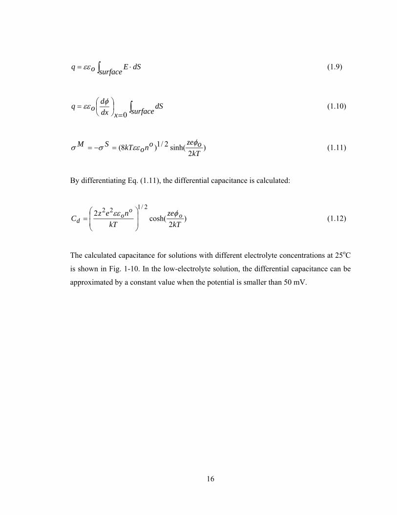
The calculated capacitance for solutions with different electrolyte concentrations at 25oC
is shown in Fig. 1-10. In the low-electrolyte solution, the differential capacitance can be
approximated by a constant value when the potential is smaller than 50 mV.
17
ElectrolyteConcentration
Fig.1-10 The predicted differential capacitance based on Gouy-Chapman theory. The
capacitance rises rapidly as the potential increases in the solution with a high electrolyte
concentration.
1.3.2 Electroosmosis
The theory of electroosmosis was first proposed by von Smoluchowski in 1921 to
explain the movement of liquid adjacent to an electrode surface under the influence of an
electric field applied parallel to the electrode-solution interface. If the electrode is
negatively charged, there are excess positive ions in the adjacent liquid. As the positive
ions move with the applied electric field, it draws the liquid along. The shear surface is a
plane parallel to the electrode, at a distance δ, as shown in Fig.1-11.
The velocity of the liquid moving in the direction parallel to the electrode rises
from zero at the shear surface to a maximum value of vslip at some distance from the
electrode. The maximum speed vslip is called the slip velocity or the electroosmotic
velocity of the liquid[31].
18
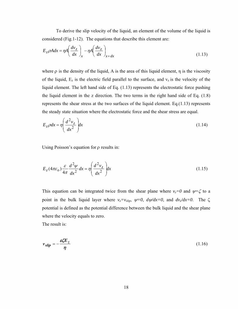
To derive the slip velocity of the liquid, an element of the volume of the liquid is
considered (Fig.1-12). The equations that describe this element are:
dxx
z
x
zz dx
dvAdx
dvAAdxE+
⎟⎠⎞
⎜⎝⎛−⎟
⎠⎞
⎜⎝⎛= ηηρ
(1.13)
where ρ is the density of the liquid, A is the area of this liquid element, η is the viscosity
of the liquid, Ez is the electric field parallel to the surface, and vz is the velocity of the
liquid element. The left hand side of Eq. (1.13) represents the electrostatic force pushing
the liquid element in the z direction. The two terms in the right hand side of Eq. (1.8)
represents the shear stress at the two surfaces of the liquid element. Eq.(1.13) represents
the steady state situation where the electrostatic force and the shear stress are equal.
dxdx
vddxE zz ⎟
⎟⎠
⎞⎜⎜⎝
⎛= 2
2ηρ (1.14)
Using Poisson’s equation for ρ results in:
dxdx
vddxdxdE z
oz ⎟⎟⎠
⎞⎜⎜⎝
⎛= 2
2
2
2
4)4( ηψπεπε (1.15)
This equation can be integrated twice from the shear plane where vz=0 and ψ=ζ to a
point in the bulk liquid layer where vz=vslip, ψ=0, dψ/dx=0, and dvz/dx=0. The ζ
potential is defined as the potential difference between the bulk liquid and the shear plane
where the velocity equals to zero.
The result is:
ηεζ z
slipE
v −= (1.16)
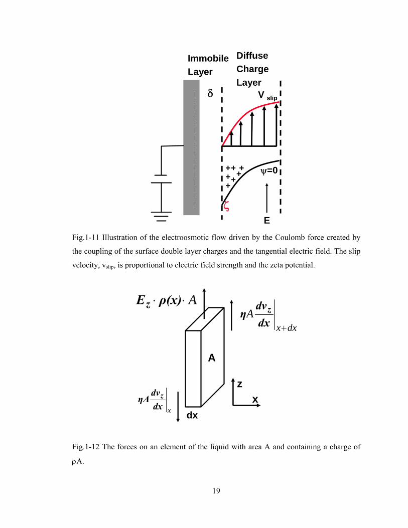
19
Diffuse Charge Layer
ζ
ψ=0
V slip
ImmobileLayer
++
++
+
++
E
δ__
__
__
__
__
__
__
__
Fig.1-11 Illustration of the electroosmotic flow driven by the Coulomb force created by
the coupling of the surface double layer charges and the tangential electric field. The slip
velocity, vslip, is proportional to electric field strength and the zeta potential.
dxxA
+dxdv
η zA⋅⋅ ρ(x)Ez
dx
zx
xdxdv
ηA z
A
Fig.1-12 The forces on an element of the liquid with area A and containing a charge of
ρA.
20
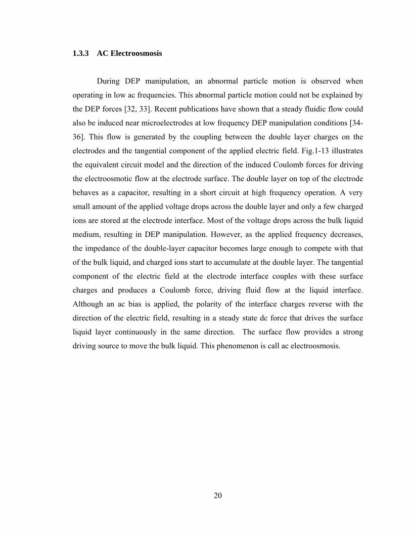
1.3.3 AC Electroosmosis
During DEP manipulation, an abnormal particle motion is observed when
operating in low ac frequencies. This abnormal particle motion could not be explained by
the DEP forces [32, 33]. Recent publications have shown that a steady fluidic flow could
also be induced near microelectrodes at low frequency DEP manipulation conditions [34-
36]. This flow is generated by the coupling between the double layer charges on the
electrodes and the tangential component of the applied electric field. Fig.1-13 illustrates
the equivalent circuit model and the direction of the induced Coulomb forces for driving
the electroosmotic flow at the electrode surface. The double layer on top of the electrode
behaves as a capacitor, resulting in a short circuit at high frequency operation. A very
small amount of the applied voltage drops across the double layer and only a few charged
ions are stored at the electrode interface. Most of the voltage drops across the bulk liquid
medium, resulting in DEP manipulation. However, as the applied frequency decreases,
the impedance of the double-layer capacitor becomes large enough to compete with that
of the bulk liquid, and charged ions start to accumulate at the double layer. The tangential
component of the electric field at the electrode interface couples with these surface
charges and produces a Coulomb force, driving fluid flow at the liquid interface.
Although an ac bias is applied, the polarity of the interface charges reverse with the
direction of the electric field, resulting in a steady state dc force that drives the surface
liquid layer continuously in the same direction. The surface flow provides a strong
driving source to move the bulk liquid. This phenomenon is call ac electroosmosis.
21
t
V
+ + + ++ _ _ _ _ _ _
Electric Field
DrivingForce
DrivingForce
++ _ _
RC C
Fig.1-13 Illustration of the mechanism of ac electroosmosis. The charged ions stored at
the electrode surface are driven by the tangential component of the electric field, causing
fluid flow. The flowing boundary layers behave as the driving source to pump flow in the
bulk liquid layer.
1.4 Reference [1] D. G. Grier, "A revolution in optical manipulation," Nature, vol. 424, pp. 810-816,
2003.
[2] L. Kremser, D. Blaas, and E. Kenndler, "Capillary electrophoresis of biological
particles: Viruses, bacteria, and eukaryotic cells," Electrophoresis, vol. 25, pp.
2282-2291, 2004.
22
[3] M. P. Hughes, "Strategies for dielectrophoretic separation in laboratory-on-a-chip
systems," Electrophoresis, vol. 23, pp. 2569-2582, 2002.
[4] H. Lee, A. M. Purdon, and R. M. Westervelt, "Manipulation of biological cells
using a microelectromagnet matrix," Applied Physics Letters, vol. 85, pp. 1063-
1065, 2004.
[5] H. M. Hertz, "Standing-Wave Acoustic Trap For Nonintrusive Positioning Of
Microparticles," Journal Of Applied Physics, vol. 78, pp. 4845-4849, 1995.
[6] N. Sundararajan, M. S. Pio, L. P. Lee, and A. A. Berlin, "Three-dimensional
hydrodynamic focusing in polydimethylsiloxane (PDMS) microchannels,"
Journal Of Microelectromechanical Systems, vol. 13, pp. 559-567, 2004.
[7] A. Ashkin, J. M. Dziedzic, J. E. Bjorkholm, and S. Chu, "Observation Of A
Single-Beam Gradient Force Optical Trap For Dielectric Particles," Optics Letters,
vol. 11, pp. 288-290, 1986.
[8] A. Ashkin, "Acceleration andTrapping of Particles by Radiation Pressure,"
Physical Review Letters, vol. 24, pp. 156, 1970.
[9] A. Ashkin and J. M. Dziedzic, "Optical Trapping And Manipulation Of Viruses
And Bacteria," Science, vol. 235, pp. 1517-1520, 1987.
[10] A. Ashkin, J. M. Dziedzic, and T. Yamane, "Optical Trapping And Manipulation
Of Single Cells Using Infrared-Laser Beams," Nature, vol. 330, pp. 769-771,
1987.
[11] J. Howard, Mechanics of Motor Proteins and the Cytoskeleton. Sunderland,
Massachusetts: Sinauer Associates, Inc., 2001.
23
[12] J. E. Curtis, B. A. Koss, and D. G. Grier, "Dynamic holographic optical
tweezers," Optics Communications, vol. 207, pp. 169-175, 2002.
[13] W. J. Hossack, E. Theofanidou, and J. Crain, "High speed holographic optical
tweezers using a ferroelectric liquid crystal microdisplay," Optics Express, vol.
11, pp. 2053-2059, 2003.
[14] A. G. J. Tibbe, B. G. de Grooth, J. Greve, P. A. Liberti, G. J. Dolan, and L.
Terstappen, "Optical tracking and detection of immunomagnetically selected and
aligned cells," Nature Biotechnology, vol. 17, pp. 1210-1213, 1999.
[15] A. Radbruch, B. Mechtold, A. Thiel, S. Miltenyi, and E. Pfluger, "High-Gradient
Magnetic Cell Sorting," in Methods In Cell Biology, Vol 42, vol. 42, Methods In
Cell Biology, 1994, pp. 387-403.
[16] J. Ugelstad, P. Stenstad, L. Kilaas, W. S. Prestvik, R. Herje, A. Berge, and E.
Hornes, "Monodisperse Magnetic Polymer Particles - New Biochemical And
Biomedical Applications," Blood Purification, vol. 11, pp. 349-369, 1993.
[17] W. D. Volkmuth and R. H. Austin, "Dna Electrophoresis In Microlithographic
Arrays," Nature, vol. 358, pp. 600-602, 1992.
[18] A. T. J. Kadaksham, P. Singh, and N. Aubry, "Dielectrophoresis of
nanoparticles," Electrophoresis, vol. 25, pp. 3625-3632, 2004.
[19] T. Muller, A. Pfennig, P. Klein, G. Gradl, M. Jager, and T. Schnelle, "The
potential of dielectrophoresis for single-cell experiments," Ieee Engineering In
Medicine And Biology Magazine, vol. 22, pp. 51-61, 2003.
24
[20] J. Tang, B. Gao, H. Z. Geng, O. D. Velev, L. C. Din, and O. Zhou, "Manipulation
and assembly of SWNTS by dielectrophoresis," Abstracts Of Papers Of The
American Chemical Society, vol. 227, pp. U1273-U1273, 2004.
[21] M. P. Hughes, H. Morgan, and F. J. Rixon, "Measuring the dielectric properties of
herpes simplex virus type 1 virions with dielectrophoresis," Biochimica Et
Biophysica Acta-General Subjects, vol. 1571, pp. 1-8, 2002.
[22] C. F. Chou, J. O. Tegenfeldt, O. Bakajin, S. S. Chan, E. C. Cox, N. Darnton, T.
Duke, and R. H. Austin, "Electrodeless dielectrophoresis of single- and double-
stranded DNA," Biophysical Journal, vol. 83, pp. 2170-2179, 2002.
[23] M. Stephens, M. S. Talary, R. Pethig, A. K. Burnett, and K. I. Mills, "The
dielectrophoresis enrichment of CD34(+) cells from peripheral blood stem cell
harvests," Bone Marrow Transplantation, vol. 18, pp. 777-782, 1996.
[24] N. Manaresi, A. Romani, G. Medoro, L. Altomare, A. Leonardi, M. Tartagni, and
R. Guerrieri, "A CMOS chip for individual cell manipulation and detection,"
IEEE J. Solid-State Circuits, vol. 38, pp. 2297-2305, 2003.
[25] T. B. Jones, Electromechanics of particles. New York: Cambridge University
Press, 1995.
[26] C. T. Okonski, "Electric Properties Of Macromolecules.5. Theory Of Ionic
Polarization In Polyelectrolytes," Journal Of Physical Chemistry, vol. 64, pp.
605-619, 1960.
[27] N. G. Green and H. Morgan, "Dielectrophoresis of submicrometer latex spheres. 1.
Experimental results," Journal Of Physical Chemistry B, vol. 103, pp. 41-50,
1999.
25
[28] A. J. Bard and L. R. Faulkner, Electrochemical methods: fundamentals and
applications. New York: John Wiley & Sons, 2001.
[29] D. L. Chapman, Philosophical Magazine, vol. 25, pp. 475, 1913.
[30] G. Gouy, Journal of Physical Chemistry, vol. 9, pp. 457, 1910.
[31] R. J. Hunter, Zeta Potential in Colloid Science. New York: Academic Press Inc.,
1981.
[32] A. Ramos, H. Morgan, N. G. Green, and A. Castellanos, "AC electric-field-
induced fluid flow in microelectrodes," Journal Of Colloid And Interface Science,
vol. 217, pp. 420-422, 1999.
[33] A. Ramos, A. Gonzalez, A. Castellanos, H. Morgan, and N. G. Green, "Fluid flow
driven by a.c. electric fields in microelectrodes," in Electrostatics 1999, vol. 163,
Institute Of Physics Conference Series, 1999, pp. 137-140.
[34] N. G. Green, A. Ramos, A. Gonzalez, H. Morgan, and A. Castellanos, "Fluid flow
induced by nonuniform ac electric fields in electrolytes on microelectrodes. I.
Experimental measurements," Physical Review E, vol. 61, pp. 4011-4018, 2000.
[35] A. Gonzalez, A. Ramos, N. G. Green, A. Castellanos, and H. Morgan, "Fluid flow
induced by nonuniform ac electric fields in electrolytes on microelectrodes. II. A
linear double-layer analysis," Physical Review E, vol. 61, pp. 4019-4028, 2000.
[36] N. G. Green, A. Ramos, A. Gonzalez, H. Morgan, and A. Castellanos, "Fluid flow
induced by nonuniform ac electric fields in electrolytes on microelectrodes. III.
Observation of streamlines and numerical simulation," Physical Review E, vol. 66,
2002.
26
CHAPTER 2
PRINCIPLE OF OPTOELECTRONIC TWEEZERS (OET)
2.1. Introduction
Electrokinetics has been widely applied in the manipulation of micro- and nano-
particles. However, parallel manipulation of individual particles remains challenging due
to wiring and interconnecting issues in addressing a large array of electrodes. One
solution is to integrate the electrode array with addressing circuits on a CMOS chip,
which increases the fabrication cost and limits the potential applications in many
biological fields. Here, we propose a novel concept called optoelectronic tweezers (OET)
that allow the control of electrokinetic mechanisms using direct optical images. Instead of
using metal wires, OET uses optical beams to pattern virtual electrodes on a
photoconductive material. This virtual electrode concept provides an elegant solution to
wiring and interconnecting issues since the light beams can propagate freely in space
without interfering with each other. By integrating the OET device with a spatial light
modulator, million-pixel resolution optical images can be created and projected onto the
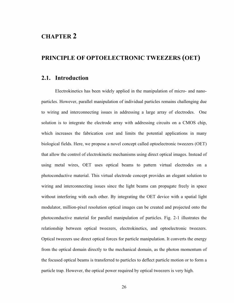
photoconductive material for parallel manipulation of particles. Fig. 2-1 illustrates the
relationship between optical tweezers, electrokinetics, and optoelectronic tweezers.
Optical tweezers use direct optical forces for particle manipulation. It converts the energy
from the optical domain directly to the mechanical domain, as the photon momentum of
the focused optical beams is transferred to particles to deflect particle motion or to form a
particle trap. However, the optical power required by optical tweezers is very high.
27
Fig. 2-1 Illustration of the energy conversion process of different manipulation
mechanisms. Unlike optical tweezers and electrokinetics, OET converts optical energy to
mechanical energy in an indirect way. The light in OET is used to trigger electrokinetic
mechanisms for particle manipulation.
On the other hand, electrokinetics converts electrical energy directly to
mechanical energy. Different electrokinetic mechanisms convert the energy in different
ways. Electrophoresis controls particle motion by using Coulomb forces to attract or
repel charged particles. Dielectrophoresis deflects particle motion through the interaction
force between a non-uniform electric field and the field-induced electric dipoles of the
particles. The particles can be either neutral or charged. Electroosmosis does not
introduce a force on the particle directly. Instead, the particles are transported by the
viscous force of a fluidic flow created by a liquid layer driven by surface charges and the
electric field parallel to the surface. However, all of the electrokinetic mechanisms have
the same wiring issues as discussed before. In order to combine the advantages of optical
tweezers and electrokinetics, OET uses an indirect method of particle manipulation. The
optical energy is first converted to electrical energy, triggering virtual electrodes on a
28
photoconductive surface. These virtual electrodes can then be used to control
electrokinetic mechanisms for particle manipulation. The light-patterned virtual
electrodes are reconfigurable, and can be actuated by a much lower optical power than
optical tweeszers. This permits OET for parallel single cell manipulation over a much
larger area than with optical tweezers techniques that use focused optical field.
Light-patterned electrodes have been widely used in xerography, which was
invented by Chester Carlson in 1942 [1]. In addition, optically-induced electrophoresis
was used to attract charged particles on indium tin oxide (ITO) and semiconductor
surfaces [2, 3] However, none of these examples has the capability of single particle
manipulation.
To achieve single-cell manipulation, the light-patterned virtual electrode has to be
sharply defined by the illumination light beam. This means the optically-generated
electron-hole pairs must have a short diffusion length before recombining. In single
crystalline silicon, the ambipolar diffusion length is ~140 µm. This is approximated from
the diffusion length of the slow carriers (Dambipolar=2DnDp/(Dn+Dp)~2Dp), holes, using the
following parameters from reference [4]: hole mobility, 400 cm2/V-sec, and carrier
lifetime, 76 µsec. This means that by using crystalline silicon as a photoconductor, one
cannot achieve high-resolution virtual electrodes. The carrier diffusion length has limited
the minimum size of the virtual electrode to ~ 280 µm, even though the light beam can be
focused to a spot size less than 1 µm. Indeed, most of the indirect bandgap crystalline
semiconductive materials have long diffusion lengths due to high carrier mobilities and
long recombination time, and are not appropriate for patterning high-resolution virtual
electrodes. For the direct bandgap III-V semiconductor such as GaAs, the short carrier
29
life time can reduce the diffusion length to ~1 µm range even though it has high carrier
mobility. The material might be cost effective.
2.2 Amorphous Silicon as a Photosensitive Material
Hydrogenated amorphous silicon (a-Si:H), which is a widely used material in the
solar cell and display industries, is a good photoconductive material for patterning high-
resolution virtual electrodes because of its short carrier diffusion length, and high optical
absorption coefficient as compared with crystalline silicon [5, 6]. The optical and
electrical properties of a-Si:H are very different from crystalline or poly-crystalline
silicon. It has an optical absorption coefficient one order of magnitude larger than
crystalline silicon near the maximum solar photon energy region of 500 nm. As a result,
the optimal active thickness of an a-Si:H solar cell, 1 µm, is much thinner than that of a
single crystalline silicon solar cell [7]. The electron transport properties in a-Si:H are also
profoundly affected by the high density of defect states. The electron mobility in
amorphous silicon is around 10 cm2/V-sec, two orders of magnitude lower than that of
single crystalline silicon. This results in a carrier diffusion length shorter than the
diffraction limit of the optical system. Experimental data has shown that the ambipolar
diffusion length in amorphous silicon is less than 100 nm [5].
The electron transport property in a-Si:H is very different from crystalline silicon
because of defect states in the mid-gap and band tails of the conduction and valence
bands. In amorphous silicon, the band edges are not as sharply defined as in crystalline
30
silicon due to the band tails. The energy band gap of amorphous silicon is around 1.85 eV,
which is much higher than the 1.12 eV in crystalline silicon [8].
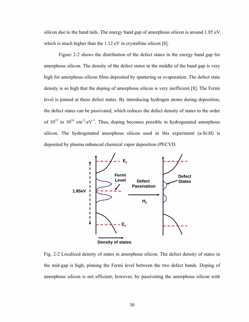
Figure 2-2 shows the distribution of the defect states in the energy band gap for
amorphous silicon. The density of the defect states in the middle of the band gap is very
high for amorphous silicon films deposited by sputtering or evaporation. The defect state
density is so high that the doping of amorphous silicon is very inefficient [8]. The Fermi
level is pinned at these defect states. By introducing hydrogen atoms during deposition,
the defect states can be passivated, which reduces the defect density of states to the order
of 1015 to 1016 cm-3-eV-1. Thus, doping becomes possible in hydrogenated amorphous
silicon. The hydrogenated amorphous silicon used in this experiment (a-Si:H) is
deposited by plasma enhanced chemical vapor deposition (PECVD.
DefectPassivation
H2
1.85eV
Density of states
FermiLevel
DefectStates
Ev
Ec
Fig. 2-2 Localized density of states in amorphous silicon. The defect density of states in
the mid-gap is high, pinning the Fermi level between the two defect bands. Doping of
amorphous silicon is not efficient; however, by passivating the amorphous silicon with
31
hydrogen atoms, the defect states can be greatly reduced to the order of 1015 to 1016
1/cm3-eV, making doping possible.
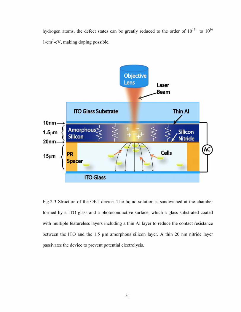
Fig.2-3 Structure of the OET device. The liquid solution is sandwiched at the chamber
formed by a ITO glass and a photoconductive surface, which a glass substrated coated
with multiple featureless layers including a thin Al layer to reduce the contact resistance
between the ITO and the 1.5 µm amorphous silicon layer. A thin 20 nm nitride layer
passivates the device to prevent potential electrolysis.
32
2.3 OET Device Design
The structure of the OET device is shown in Fig. 2-3. It is a sandwich structure
that consists of two surfaces: transparent and conductive ITO (heavily doped Indium Tin
Oxide) glass and a photoconductive surface made of ITO glass coated with multiple
featureless layers including 10 nm of aluminum, 1.5 µm of intrinsic a-Si:H, and 20 nm of
silicon nitride. The thickness of the chamber for the liquid solution containing the
particles of interest is defined by the spacer between the top and the bottom surfaces. The
chamber thickness can be adjusted to tune the electric field strength and to accommodate
particles of different sizes. The aluminum layer is used to reduce the contact resistance
between the ITO and the amorphous silicon layer. The thickness of this metal layer is less
than 10 nm to prevent blocking of the incident light beam. The 20-nm silicon nitride layer
is to prevent electrolysis during low frequency operation, which causes bubbling in the
liquid layer. The insulating silicon nitride layer will not block the ac signal at high ac
frequency, as it behaves as a capacitor and a high pass filter. As an ac signal is applied to
the top and the bottom electrodes, the majority of the applied voltage drops across the
amorphous silicon layer since it has high electrical impedance in its dark state. The dark
conductivity of the amorphous silicon is around 10-8 S/m, allowing only a very limited
electric field in the liquid layer, which produces no DEP force. When a light beam
illuminates the amorphous silicon layer, the light-generated electron-holes pairs increase
the conductivity of the amorphous silicon layer by several orders of magnitude,
depending on the intensity of the illumination. Reported data has shown that the
photoconductivity of amorphous silicon increases by five orders of magnitude under an
illumination intensity of 100 W/cm2 [9]. The increase in the conductivity of the
33
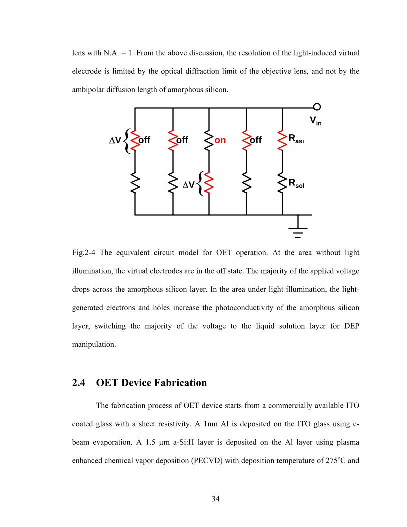
amorphous silicon layer shifts the majority of the voltage drop to the liquid layer as
shown in the equivalent circuit model in Fig.2-4. and creates a non-uniform electric field
near the illuminated spots. The cells or the particles near the illuminated spots are
polarized and experience DEP forces due to the interaction of the induced dipoles and the
local electric field. Particles experiencing positive DEP forces will be attracted to the
illuminated spots, while particles experiencing negative DEP forces will be pushed away
from the illuminated spots. The particles can be continuously addressed at any position
on the two-dimensional surface by canning the light beams across the surface.
The resolution of the light-patterned virtual electrode is limited by two factors: the
ambipolar diffusion length of the carriers in the amorphous silicon layer and the optical
diffraction limit of the focused light spot. The electron and hole concentration at the
illuminated spot is higher than the neighboring area, resulting in lateral carrier diffusion
away from the illuminated spot. In our OET device, the number of light-generated
carriers is far more than the intrinsic carrier concentration in the conduction band. The
numbers of light-generated electrons and holes are almost equal, resulting in an
ambipolar diffusion process. The ambipolar diffusion length is mainly determined by the
mobility of the slow carrier (the hole for amorphous silicon), and the recombination time
of the carriers. Previous literature has reported that the ambipolar diffusion length of
amorphous silicon is less than 100 nm [5]. The second limiting factor for the virtual
electrode resolution is the optical diffraction limit of the optical system. From Fraunhofer
diffraction theory, the minimum spot size that can be formed by an objective lens is
1.22λ/N.A., where N.A. is the numerical aperture of the objective lens. For example, 0.77
µm is the minimum spot size that can be formed using a 633 nm laser and an objective
34
lens with N.A. = 1. From the above discussion, the resolution of the light-induced virtual
electrode is limited by the optical diffraction limit of the objective lens, and not by the
ambipolar diffusion length of amorphous silicon.
Vin
on Rasi
Rsol
ΔV
ΔV
{{
offoff off
Fig.2-4 The equivalent circuit model for OET operation. At the area without light
illumination, the virtual electrodes are in the off state. The majority of the applied voltage
drops across the amorphous silicon layer. In the area under light illumination, the light-
generated electrons and holes increase the photoconductivity of the amorphous silicon
layer, switching the majority of the voltage to the liquid solution layer for DEP
manipulation.
2.4 OET Device Fabrication
The fabrication process of OET device starts from a commercially available ITO
coated glass with a sheet resistivity. A 1nm Al is deposited on the ITO glass using e-
beam evaporation. A 1.5 µm a-Si:H layer is deposited on the Al layer using plasma
enhanced chemical vapor deposition (PECVD) with deposition temperature of 275oC and
35
silane (SiH4) flow rate 9 sccm. Due to the limitation of our facility, no extra hydrogen gas
is added during the deposition to passivate the dangling bonds. This increases the defect
density in a-Si:H and the optical power of OET actuation. On top of the a-Si:H layer is a
20 nm silicon nitride layer deposited by PECVD. This silicon nitride layer, designed to
prevent electrolysis, can be removed if OET is operated in high ac frequency and low ac
bias range.
To sandwich the liquid between the ITO and the photoconductive surfaces, a
liquid droplet is pipetted on the photoconductive surface. The ITO glass is then glued to
the photoconductive surface using double-side tape, enclosing the liquid droplet between
the two surfaces and giving a spacing ~ 100 µm. To get different gap spacing, various
photoresist can be spin-coated at different speed and patterned as the spacer material.
To increase the photoconductivity of the OET device, we replaced the Al layer
with a 50 nm heavily doped n+ a-Si:H to further decrease the contact resistance between
the ITO and the intrinsic a-Si:H layer (This structure is shown in Chap. 4.2). This n+ layer
also reduces the loss due to the optical reflection in the metal and semiconductor interface
and increases the optical transmission to the intrinsic layer. This further lowers the optical
power for OET actuation. To get a better quality a-Si:H having less defect density, we
have used the foundry service to deposit the n+ and the intrinsic a-Si:H layers (SDtech
Inc., http://www.sdtech.co.kr). The company claims the spin defect density is ~ 1015 /cm3.
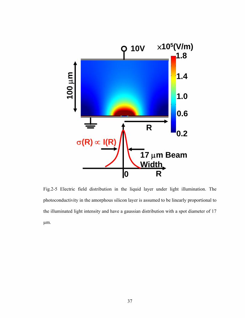
2.5 Simulated electric field distribution
We use the dc electrostatic module in FEMLAB for finite element simulations of
the electric field strength and its distribution in the solution of the OET device. In this
36
simulation, the liquid conductivity is assumed to be 0.01 S/m and the dark conductivity of
the amorphous silicon layer is 10-8 S/m. In the area under light illumination, we assume
there is no vertical variation of the photoconductivity and the radial distribution of the
photoconductivity is linearly proportional to the illumination intensity, which has a radial
gaussian distribution and a FWHM spot diameter of 17 µm. The result (Fig.2-5) shows
that the strongest electric field occurs near the surface of the illuminated spot. There is an
electric field gradient in both lateral and vertical directions, meaning that the generated
DEP forces will pull the nearby particles towards the surface of the virtual electrode if a
positive DEP force is induced, or in the opposite direction if a negative DEP force is
induced. To simulate the OET response to illumination power, we define a normalized
photoconductivity c, which is the ratio of σphoto/σm, where σphoto is the maximum
conductivity at the peak of the gaussian beam and σm is the medium conductivity.
37
×105(V/m)10V
100 μm
0.2R
17 μm Beam Width
σ(R) ∝ I(R)
R0
0.6
1.0
1.4
1.8
Fig.2-5 Electric field distribution in the liquid layer under light illumination. The
photoconductivity in the amorphous silicon layer is assumed to be linearly proportional to
the illuminated light intensity and have a gaussian distribution with a spot diameter of 17
µm.
38
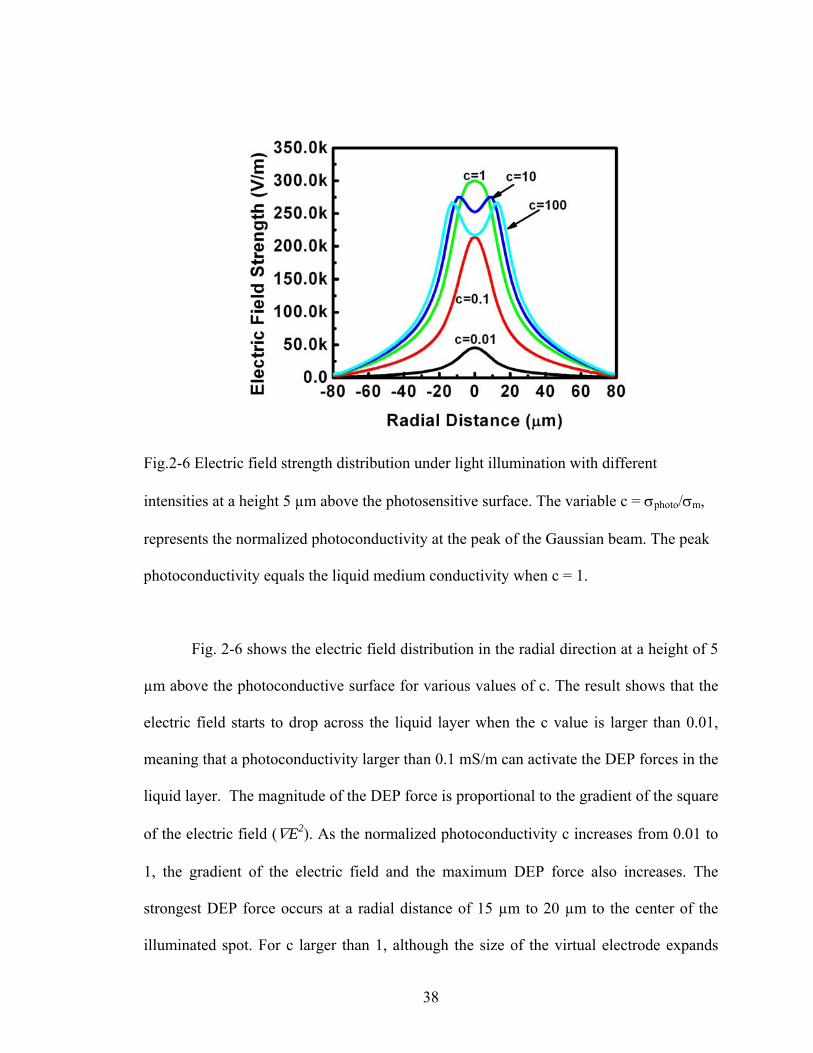
Fig.2-6 Electric field strength distribution under light illumination with different
intensities at a height 5 µm above the photosensitive surface. The variable c = σphoto/σm,
represents the normalized photoconductivity at the peak of the Gaussian beam. The peak
photoconductivity equals the liquid medium conductivity when c = 1.
Fig. 2-6 shows the electric field distribution in the radial direction at a height of 5
µm above the photoconductive surface for various values of c. The result shows that the
electric field starts to drop across the liquid layer when the c value is larger than 0.01,
meaning that a photoconductivity larger than 0.1 mS/m can activate the DEP forces in the
liquid layer. The magnitude of the DEP force is proportional to the gradient of the square
of the electric field (∇E2). As the normalized photoconductivity c increases from 0.01 to
1, the gradient of the electric field and the maximum DEP force also increases. The
strongest DEP force occurs at a radial distance of 15 µm to 20 µm to the center of the
illuminated spot. For c larger than 1, although the size of the virtual electrode expands
39
with the increased optical power, the maximum DEP force remains almost constant. This
can be found from the maximum slope of the electric field when c > 1. This implies that
the virtual electrode has been fully turned on, and further increases the photoconductivity
does not increase the maximum DEP forces, but only serves to increase the effective size
of the light-induced virtual electrode. There is one significant difference between the
curves for c < 1 and the curves for c > 1. In the case of c < 1, there is only one peak for
the electric field distribution, meaning that the positive DEP forces can concentrate
positive DEP particles to the center of the illuminated spot. For c > 1, a double-peak
profile emerges. Positive DEP forces will concentrate the particles to the edge, not the
center, of the virtual electrode. The effective range of the light-induced DEP forces is
also shown in Fig. 2-6. The light-induced DEP forces extend to ~ 80 µm in the radial
direction from the center of the illuminated spot. However, the strongest DEP forces
occur at a radial distance between 20 ~ 30 µm for all c values shown in Fig.2-6.
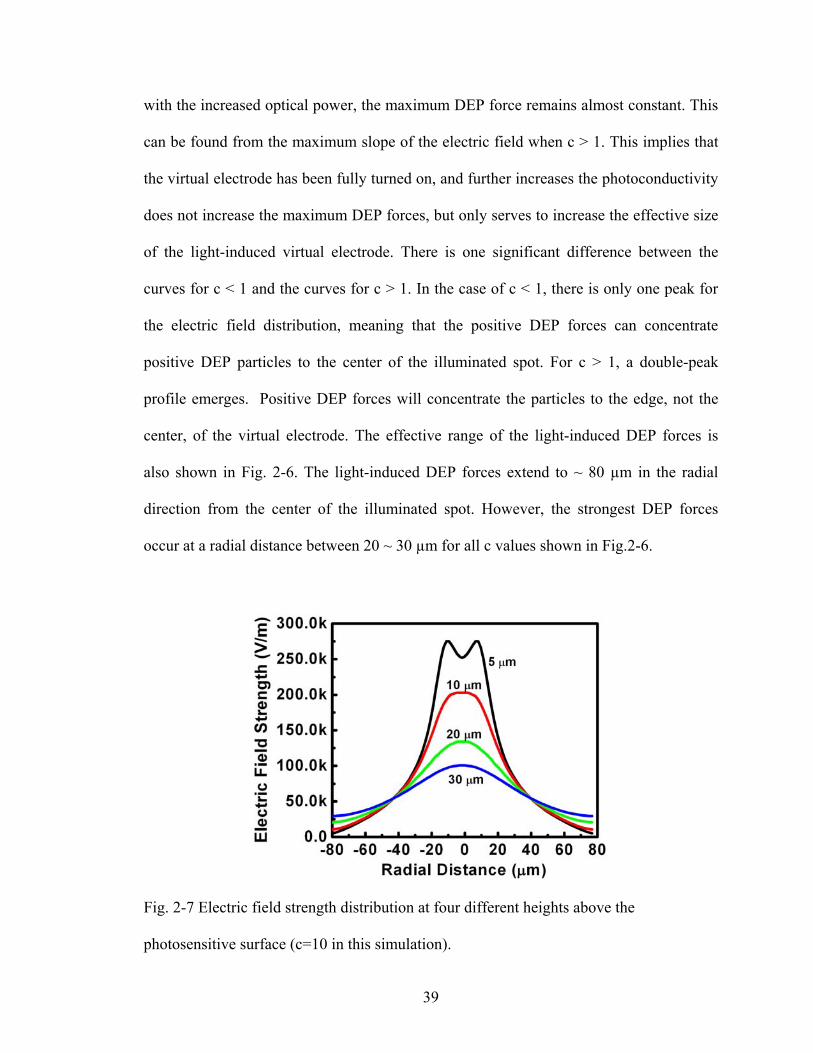
Fig. 2-7 Electric field strength distribution at four different heights above the
photosensitive surface (c=10 in this simulation).
40
To understand the DEP forces in the vertical direction, the electric field strength
at four different heights above the photoconductive surface for c=10 are plotted in Fig. 2-
7. The strongest electric field occurs right above the virtual electrode, and decays in the
vertical direction, resulting in a vertical DEP force that can be applied to concentrate
positive DEP particles onto the photoconductive surface. Near the photoconductive
surface, the electric field decays sharply in the lateral direction; however, at a position
higher than 30 µm above the photoconductive surface, the lateral gradient of the
electrical field is small, resulting in a small lateral DEP force even though the electric
field strength is still large. Thus, DEP manipulation of particles would only be effective
at positions near the photoconductive surface in both the lateral and vertical directions.
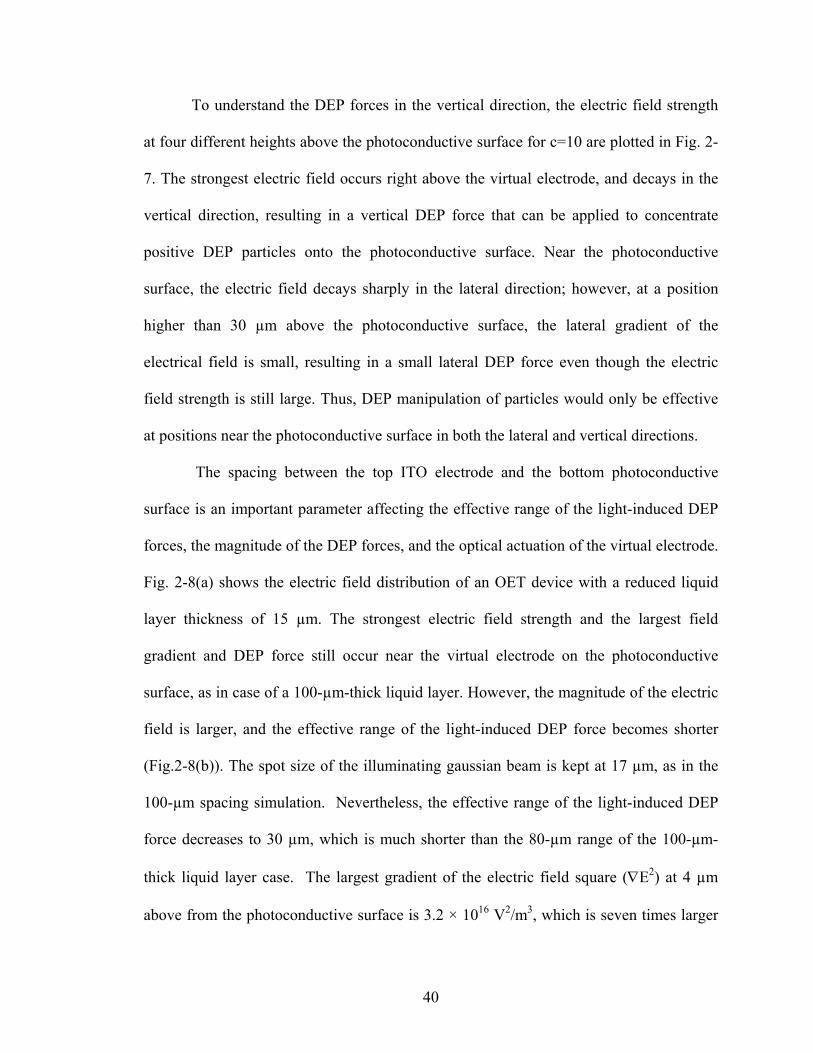
The spacing between the top ITO electrode and the bottom photoconductive
surface is an important parameter affecting the effective range of the light-induced DEP
forces, the magnitude of the DEP forces, and the optical actuation of the virtual electrode.
Fig. 2-8(a) shows the electric field distribution of an OET device with a reduced liquid
layer thickness of 15 µm. The strongest electric field strength and the largest field
gradient and DEP force still occur near the virtual electrode on the photoconductive
surface, as in case of a 100-µm-thick liquid layer. However, the magnitude of the electric
field is larger, and the effective range of the light-induced DEP force becomes shorter
(Fig.2-8(b)). The spot size of the illuminating gaussian beam is kept at 17 µm, as in the
100-µm spacing simulation. Nevertheless, the effective range of the light-induced DEP
force decreases to 30 µm, which is much shorter than the 80-µm range of the 100-µm-
thick liquid layer case. The largest gradient of the electric field square (∇E2) at 4 µm
above from the photoconductive surface is 3.2 × 10¹⁶ V2/m3, which is seven times larger
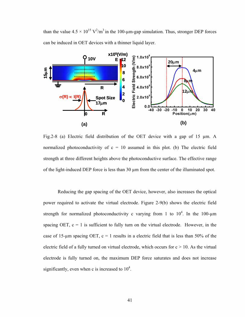
41
than the value 4.5 × 10¹⁵ V2/m3 in the 100-µm-gap simulation. Thus, stronger DEP forces
can be induced in OET devices with a thinner liquid layer.
x105(V/m)10V
0
R
Spot Size17μm
σ(R) ∝ I(R)
R0
E
2
6
1012
4
8
15μm
x105(V/m)10V
0
R
Spot Size17μm
σ(R) ∝ I(R)
R0
E
2
6
1012
4
8
15μm 4μm
8μm
12μm
20μm
4μm
8μm
12μm
20μm
(a) (b)
Fig.2-8 (a) Electric field distribution of the OET device with a gap of 15 µm. A
normalized photoconductivity of c = 10 assumed in this plot. (b) The electric field
strength at three different heights above the photoconductive surface. The effective range
of the light-induced DEP force is less than 30 µm from the center of the illuminated spot.
Reducing the gap spacing of the OET device, however, also increases the optical
power required to activate the virtual electrode. Figure 2-9(b) shows the electric field
strength for normalized photoconductivity c varying from 1 to 104. In the 100-µm
spacing OET, c = 1 is sufficient to fully turn on the virtual electrode. However, in the
case of 15-µm spacing OET, c = 1 results in a electric field that is less than 50% of the
electric field of a fully turned on virtual electrode, which occurs for c > 10. As the virtual
electrode is fully turned on, the maximum DEP force saturates and does not increase
significantly, even when c is increased to 104.
42
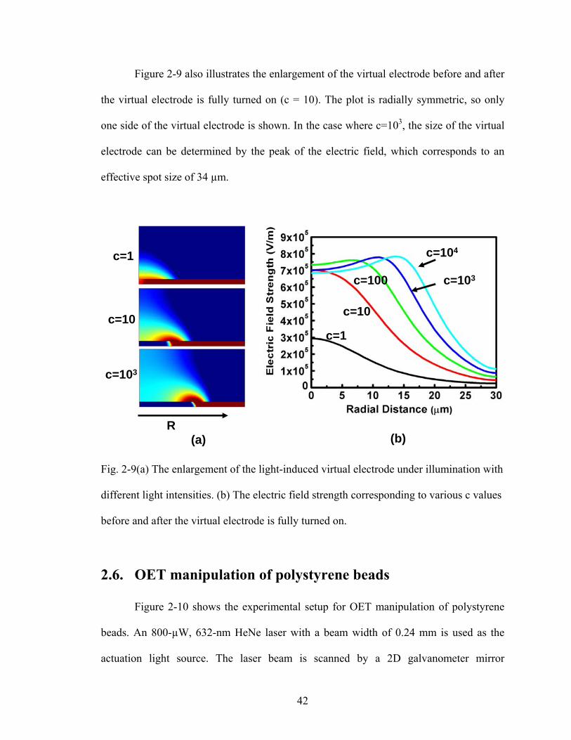
Figure 2-9 also illustrates the enlargement of the virtual electrode before and after
the virtual electrode is fully turned on (c = 10). The plot is radially symmetric, so only
one side of the virtual electrode is shown. In the case where c=103, the size of the virtual
electrode can be determined by the peak of the electric field, which corresponds to an
effective spot size of 34 µm.
c=103
c=10
c=1
R
c=1
c=10
c=100
c=104
c=103
(a) (b)
Fig. 2-9(a) The enlargement of the light-induced virtual electrode under illumination with
different light intensities. (b) The electric field strength corresponding to various c values
before and after the virtual electrode is fully turned on.
2.6. OET manipulation of polystyrene beads
Figure 2-10 shows the experimental setup for OET manipulation of polystyrene
beads. An 800-µW, 632-nm HeNe laser with a beam width of 0.24 mm is used as the
actuation light source. The laser beam is scanned by a 2D galvanometer mirror
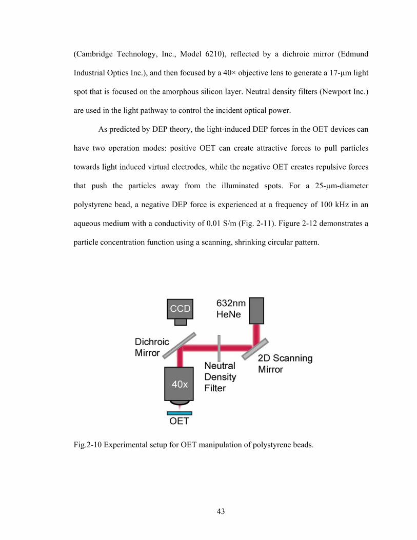
43
(Cambridge Technology, Inc., Model 6210), reflected by a dichroic mirror (Edmund
Industrial Optics Inc.), and then focused by a 40× objective lens to generate a 17-µm light
spot that is focused on the amorphous silicon layer. Neutral density filters (Newport Inc.)
are used in the light pathway to control the incident optical power.
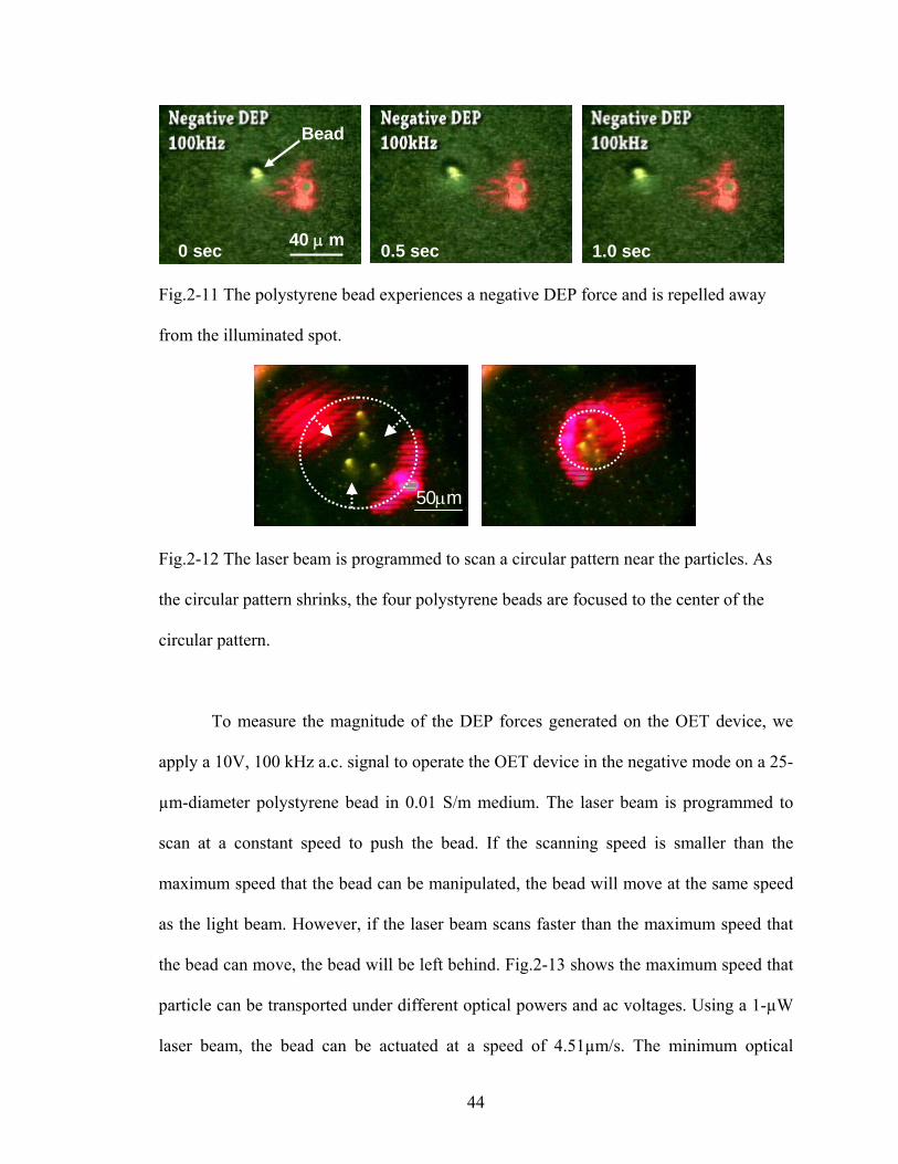
As predicted by DEP theory, the light-induced DEP forces in the OET devices can
have two operation modes: positive OET can create attractive forces to pull particles
towards light induced virtual electrodes, while the negative OET creates repulsive forces
that push the particles away from the illuminated spots. For a 25-µm-diameter
polystyrene bead, a negative DEP force is experienced at a frequency of 100 kHz in an
aqueous medium with a conductivity of 0.01 S/m (Fig. 2-11). Figure 2-12 demonstrates a
particle concentration function using a scanning, shrinking circular pattern.
Fig.2-10 Experimental setup for OET manipulation of polystyrene beads.
44
Fig.2-11 The polystyrene bead experiences a negative DEP force and is repelled away
from the illuminated spot.
50μm50μm
Fig.2-12 The laser beam is programmed to scan a circular pattern near the particles. As
the circular pattern shrinks, the four polystyrene beads are focused to the center of the
circular pattern.
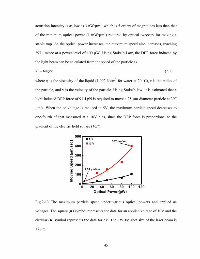
To measure the magnitude of the DEP forces generated on the OET device, we
apply a 10V, 100 kHz a.c. signal to operate the OET device in the negative mode on a 25-
µm-diameter polystyrene bead in 0.01 S/m medium. The laser beam is programmed to
scan at a constant speed to push the bead. If the scanning speed is smaller than the
maximum speed that the bead can be manipulated, the bead will move at the same speed
as the light beam. However, if the laser beam scans faster than the maximum speed that
the bead can move, the bead will be left behind. Fig.2-13 shows the maximum speed that
particle can be transported under different optical powers and ac voltages. Using a 1-µW
laser beam, the bead can be actuated at a speed of 4.51µm/s. The minimum optical
0 sec 0.5 sec 1.0 sec40 μ m
Bead
45
actuation intensity is as low as 3 nW/µm2, which is 5 orders of magnitudes less than that
of the minimum optical power (1 mW/µm2) required by optical tweezers for making a
stable trap. As the optical power increases, the maximum speed also increases, reaching
397 µm/sec at a power level of 100 µW. Using Stoke’s Law, the DEP force induced by
the light beam can be calculated from the speed of the particle as
rvF πη6= (2.1)
where η is the viscosity of the liquid (1.002 Ns/m2 for water at 20 oC), r is the radius of
the particle, and v is the velocity of the particle. Using Stoke’s law, it is estimated that a
light-induced DEP force of 93.4 pN is required to move a 25-μm-diameter particle at 397
µm/s. When the ac voltage is reduced to 5V, the maximum particle speed decreases to
one-fourth of that measured at a 10V bias, since the DEP force is proportional to the
gradient of the electric field square (∇E2).
Fig.2-13 The maximum particle speed under various optical powers and applied ac
voltages. The square (■) symbol represents the data for an applied voltage of 10V and the
circular (●) symbol represents the data for 5V. The FWHM spot size of the laser beam is
17 µm.
46
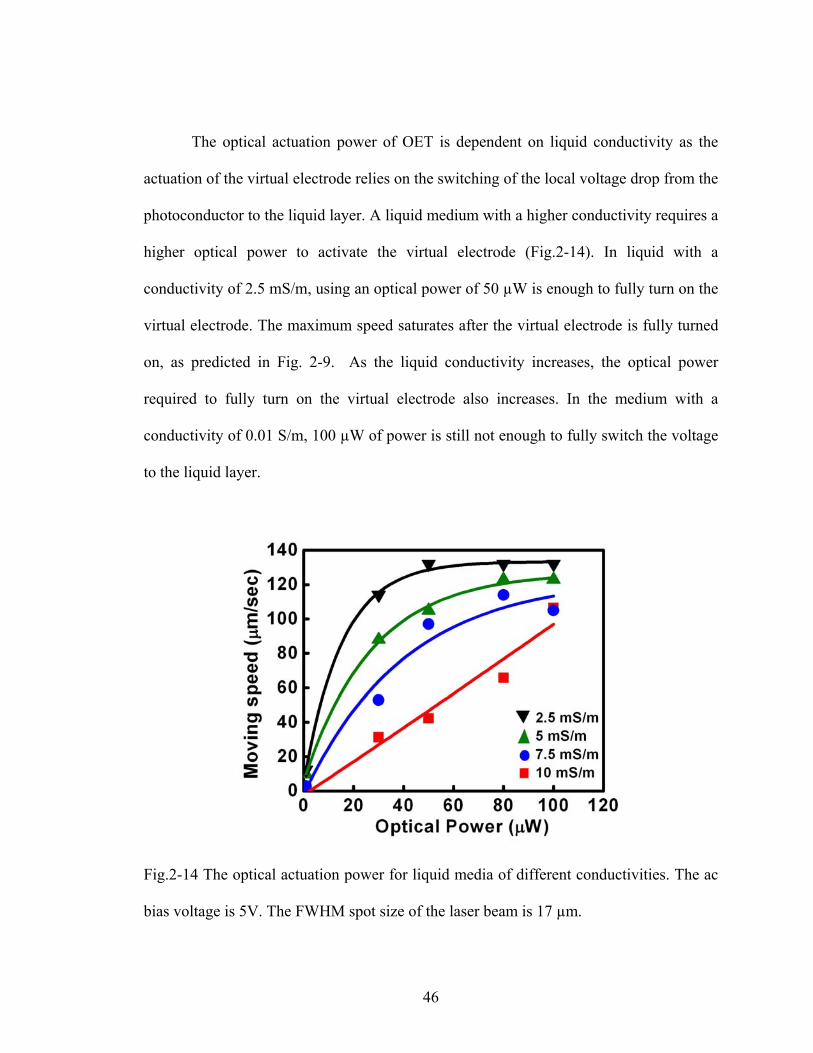
The optical actuation power of OET is dependent on liquid conductivity as the
actuation of the virtual electrode relies on the switching of the local voltage drop from the
photoconductor to the liquid layer. A liquid medium with a higher conductivity requires a
higher optical power to activate the virtual electrode (Fig.2-14). In liquid with a
conductivity of 2.5 mS/m, using an optical power of 50 µW is enough to fully turn on the
virtual electrode. The maximum speed saturates after the virtual electrode is fully turned
on, as predicted in Fig. 2-9. As the liquid conductivity increases, the optical power
required to fully turn on the virtual electrode also increases. In the medium with a
conductivity of 0.01 S/m, 100 µW of power is still not enough to fully switch the voltage
to the liquid layer.
Fig.2-14 The optical actuation power for liquid media of different conductivities. The ac
bias voltage is 5V. The FWHM spot size of the laser beam is 17 µm.
47
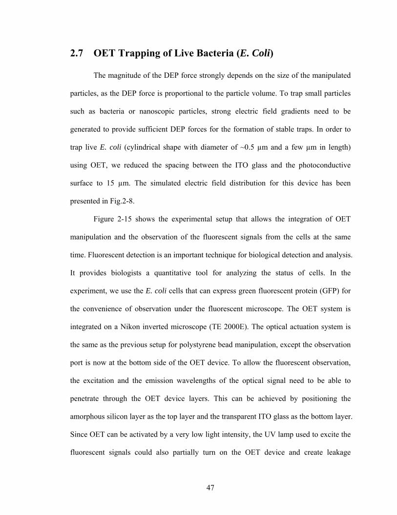
2.7 OET Trapping of Live Bacteria (E. Coli)
The magnitude of the DEP force strongly depends on the size of the manipulated
particles, as the DEP force is proportional to the particle volume. To trap small particles
such as bacteria or nanoscopic particles, strong electric field gradients need to be
generated to provide sufficient DEP forces for the formation of stable traps. In order to
trap live E. coli (cylindrical shape with diameter of ~0.5 µm and a few µm in length)
using OET, we reduced the spacing between the ITO glass and the photoconductive
surface to 15 µm. The simulated electric field distribution for this device has been
presented in Fig.2-8.
Figure 2-15 shows the experimental setup that allows the integration of OET
manipulation and the observation of the fluorescent signals from the cells at the same
time. Fluorescent detection is an important technique for biological detection and analysis.
It provides biologists a quantitative tool for analyzing the status of cells. In the
experiment, we use the E. coli cells that can express green fluorescent protein (GFP) for
the convenience of observation under the fluorescent microscope. The OET system is
integrated on a Nikon inverted microscope (TE 2000E). The optical actuation system is
the same as the previous setup for polystyrene bead manipulation, except the observation
port is now at the bottom side of the OET device. To allow the fluorescent observation,
the excitation and the emission wavelengths of the optical signal need to be able to
penetrate through the OET device layers. This can be achieved by positioning the
amorphous silicon layer as the top layer and the transparent ITO glass as the bottom layer.
Since OET can be activated by a very low light intensity, the UV lamp used to excite the
fluorescent signals could also partially turn on the OET device and create leakage
48
currents that could turn on the virtual electrodes in regions that do not have laser
illumination. This could potentially be serious for OET manipulation, depending on the
light intensity and the wavelength of the excitation signals. Figure 2-16 shows the
wavelength-dependent optical attenuation of the amorphous silicon layer using the
absorption coefficients from [10] . Wavelengths shorter than 600 nm are strongly
absorbed by the amorphous silicon, and are attenuated within 0.1 µm from the incident
surface. In the OET devices, the amorphous silicon layer has a thickness of 1 µm to 1.5
µm. Optical actuation using a wavelength shorter than 600 nm thus only increases the
photoconductivity near the surface of the amorphous silicon, keeping the overall
conductivity of the photoconductive layer low. This keeps the virtual electrode in the off
state. In most biological experiments, the excitation wavelengths of the fluorescent
signals are shorter than 600 nm, and the emission signals from the fluorescent particles to
weak to affect the OET operation. Thus, the effect of fluorescent excitation and emission
on the actuation of OET is limited, enabling the possibility of integrating OET with a
fluorescent microscope.
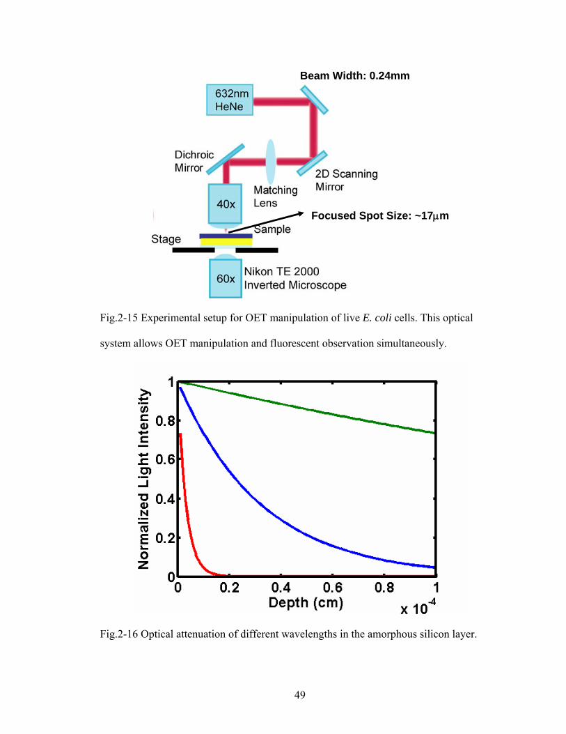
49
Beam Width: 0.24mm
Focused Spot Size: ~17μm
Fig.2-15 Experimental setup for OET manipulation of live E. coli cells. This optical
system allows OET manipulation and fluorescent observation simultaneously.
Fig.2-16 Optical attenuation of different wavelengths in the amorphous silicon layer.
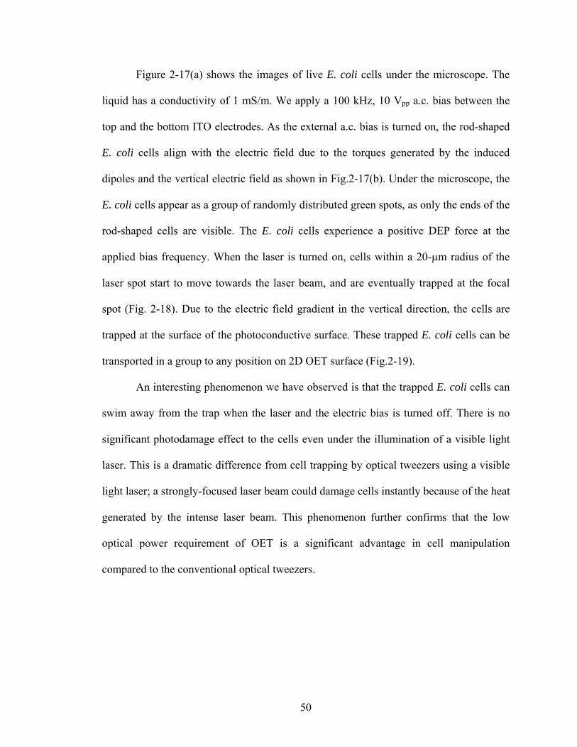
50
Figure 2-17(a) shows the images of live E. coli cells under the microscope. The
liquid has a conductivity of 1 mS/m. We apply a 100 kHz, 10 Vpp a.c. bias between the
top and the bottom ITO electrodes. As the external a.c. bias is turned on, the rod-shaped
E. coli cells align with the electric field due to the torques generated by the induced
dipoles and the vertical electric field as shown in Fig.2-17(b). Under the microscope, the
E. coli cells appear as a group of randomly distributed green spots, as only the ends of the
rod-shaped cells are visible. The E. coli cells experience a positive DEP force at the
applied bias frequency. When the laser is turned on, cells within a 20-µm radius of the
laser spot start to move towards the laser beam, and are eventually trapped at the focal
spot (Fig. 2-18). Due to the electric field gradient in the vertical direction, the cells are
trapped at the surface of the photoconductive surface. These trapped E. coli cells can be
transported in a group to any position on 2D OET surface (Fig.2-19).
An interesting phenomenon we have observed is that the trapped E. coli cells can
swim away from the trap when the laser and the electric bias is turned off. There is no
significant photodamage effect to the cells even under the illumination of a visible light
laser. This is a dramatic difference from cell trapping by optical tweezers using a visible
light laser; a strongly-focused laser beam could damage cells instantly because of the heat
generated by the intense laser beam. This phenomenon further confirms that the low
optical power requirement of OET is a significant advantage in cell manipulation
compared to the conventional optical tweezers.
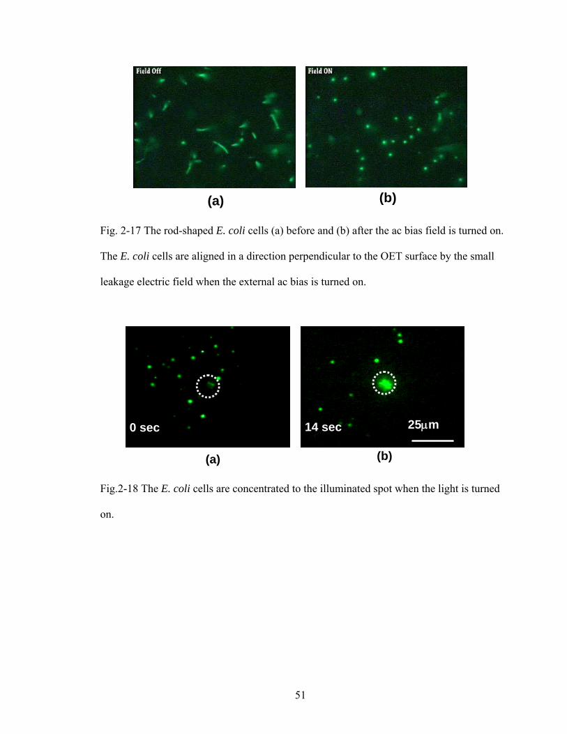
51
(a) (b)
Fig. 2-17 The rod-shaped E. coli cells (a) before and (b) after the ac bias field is turned on.
The E. coli cells are aligned in a direction perpendicular to the OET surface by the small
leakage electric field when the external ac bias is turned on.
25μm0 sec 14 sec
(a) (b)
Fig.2-18 The E. coli cells are concentrated to the illuminated spot when the light is turned
on.
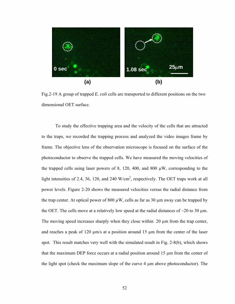
52
25μm1.08 sec0 sec
(a) (b)
Fig.2-19 A group of trapped E. coli cells are transported to different positions on the two
dimensional OET surface.
To study the effective trapping area and the velocity of the cells that are attracted
to the traps, we recorded the trapping process and analyzed the video images frame by
frame. The objective lens of the observation microscope is focused on the surface of the
photoconductor to observe the trapped cells. We have measured the moving velocities of
the trapped cells using laser powers of 8, 120, 400, and 800 µW, corresponding to the
light intensities of 2.4, 36, 120, and 240 W/cm2, respectively. The OET traps work at all
power levels. Figure 2-20 shows the measured velocities versus the radial distance from
the trap center. At optical power of 800 µW, cells as far as 30 µm away can be trapped by
the OET. The cells move at a relatively low speed at the radial distances of ~20 to 30 µm.
The moving speed increases sharply when they close within 20 µm from the trap center,
and reaches a peak of 120 µm/s at a position around 15 µm from the center of the laser
spot. This result matches very well with the simulated result in Fig. 2-8(b), which shows
that the maximum DEP force occurs at a radial position around 15 µm from the center of
the light spot (check the maximum slope of the curve 4 µm above photoconductor). The
53
cell velocity is a function of the optical power. The peak velocity increases from the 26
µm/s at 8 µW to the 90 µm/s at 120 µW. Above 120 µW, the peak velocity increases
slowly, and eventually saturates at about 200 µW (Fig.2-20(b)). This can be explained by
the following: when the optical power is lower than 120 µW, the virtual electrode is not
fully turned on. Above 200 µW, the virtual electrode is fully turned on, switching most of
the voltage drop to the liquid layer. Further increasing the optical power does not increase
the electric field strength. However, the effective size of the virtual electrode still
increases with higher optical powers. This is why the position where the peak velocity
occurs is farther away from the trap center for higher optical powers.
It should be pointed out that the saturation of the photoconductivity is another
reason that could cause the saturation effect of the peak velocity. If the saturated
photoconductivity is not high enough to fully turn on the virtual electrode, the
phenomenon of the saturation of the peak velocity and the enlargement of the virtual
electrode can also be observed. The only difference would be that the magnitude of the
peak velocity does not reach the value when the virtual electrode is truly turned on. The
reason for photoconductivity saturation will be discussed in detail later in this chapter.
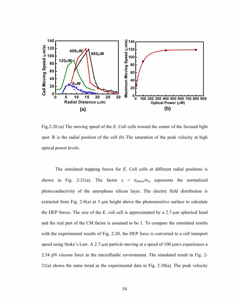
54
Fig.2-20 (a) The moving speed of the E. Coli cells toward the center of the focused light
spot. R is the radial position of the cell (b) The saturation of the peak velocity at high
optical power levels.
The simulated trapping forces for E. Coli cells at different radial positions is
shown in Fig. 2-21(a). The factor c = σphoto/σm represents the normalized
photoconductivity of the amorphous silicon layer. The electric field distribution is
extracted from Fig. 2-8(a) at 3 µm height above the photosensitive surface to calculate
the DEP forces. The size of the E. coli cell is approximated by a 2.7-µm spherical bead
and the real part of the CM factor is assumed to be 1. To compare the simulated results
with the experimental results of Fig. 2-20, the DEP force is converted to a cell transport
speed using Stoke’s Law. A 2.7-µm particle moving at a speed of 100 µm/s experiences a
2.54 pN viscous force in the microfluidic environment. The simulated result in Fig. 2-
21(a) shows the same trend as the experimental data in Fig. 2-20(a). The peak velocity
(a) (b)
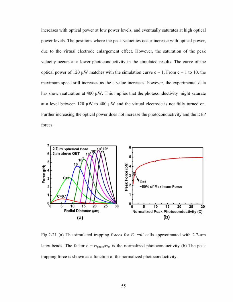
55
increases with optical power at low power levels, and eventually saturates at high optical
power levels. The positions where the peak velocities occur increase with optical power,
due to the virtual electrode enlargement effect. However, the saturation of the peak
velocity occurs at a lower photoconductivity in the simulated results. The curve of the
optical power of 120 µW matches with the simulation curve c = 1. From c = 1 to 10, the
maximum speed still increases as the c value increases; however, the experimental data
has shown saturation at 400 µW. This implies that the photoconductivity might saturate
at a level between 120 µW to 400 µW and the virtual electrode is not fully turned on.
Further increasing the optical power does not increase the photoconductivity and the DEP
forces.
Fig.2-21 (a) The simulated trapping forces for E. coli cells approximated with 2.7-µm
latex beads. The factor c = σphoto/σm is the normalized photoconductivity (b) The peak
trapping force is shown as a function of the normalized photoconductivity.
(a) (b)
Spherical Bead
56
2.8 AC Frequency Range for OET Operation
OET devices consist of multiple featureless layers including a 1~1.5 µm
amorphous silicon layer, a 20 nm nitride layer, and a liquid solution layer that can be
varied from 10 µm to 100 µm depending on the application (Fig. 2-22(a)). Between the
interface of the solid and liquid layer, there is an electric double layer (EDL) which
behaves as a capacitor. When an external a.c. bias is applied through the top and the
bottom electrodes, these multiple layers can be modeled as serially connected lumped
circuit elements (Fig. 2-22(b)). In ideal OET operation, all the applied voltage drops
across the amorphous silicon layer in the dark; under illumination, all the voltage is
dropped across the liquid layer. However, in a more realistic model, some of the voltage
may drop across the liquid layer in the dark, creating a leakage electric field. Under light
illumination, some of the voltage may drop across the insulating layers or the EDL,
decreasing the electric field strength and the DEP forces induced in the liquid layer. To
solve these issues, the thickness of the insulation layer and the frequencies of the applied
signals need to be carefully selected.
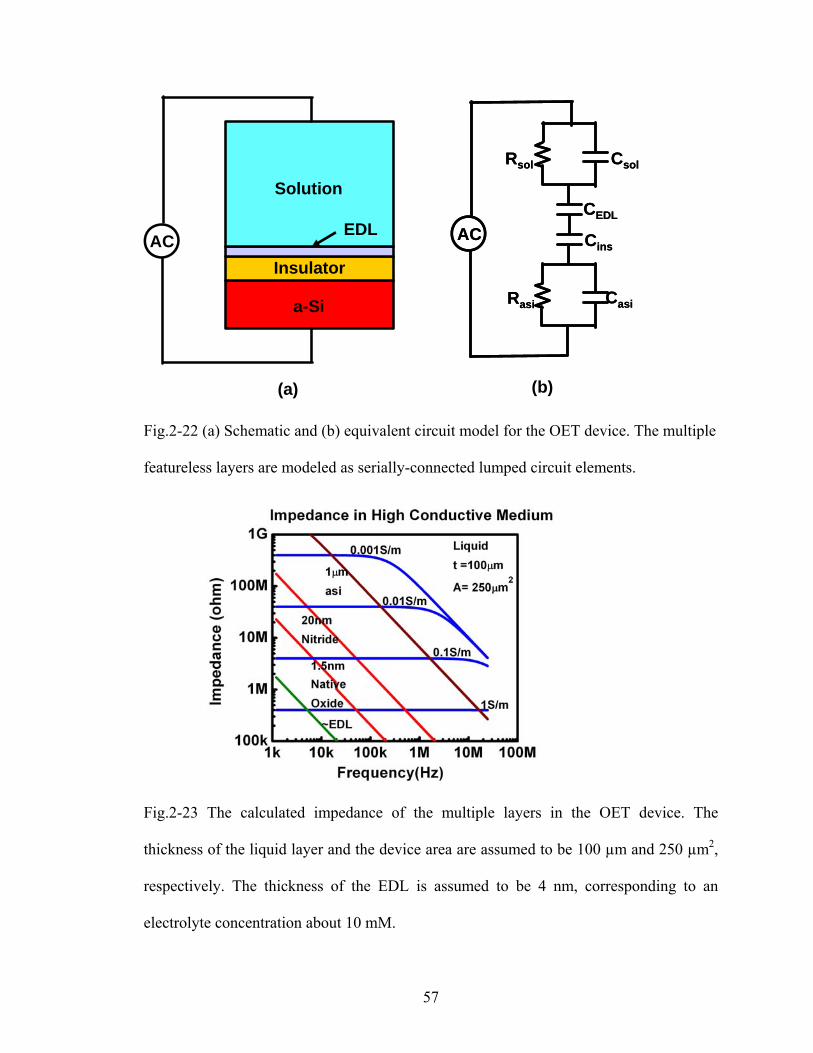
57
AC
Casi
Cins
CEDL
CsolRsol
Rasi
AC
Casi
Cins
CEDL
CsolRsol
Rasi
AC
Solution
a-Si
Insulator
EDL
(a) (b)
Fig.2-22 (a) Schematic and (b) equivalent circuit model for the OET device. The multiple
featureless layers are modeled as serially-connected lumped circuit elements.
Fig.2-23 The calculated impedance of the multiple layers in the OET device. The
thickness of the liquid layer and the device area are assumed to be 100 µm and 250 µm2,
respectively. The thickness of the EDL is assumed to be 4 nm, corresponding to an
electrolyte concentration about 10 mM.
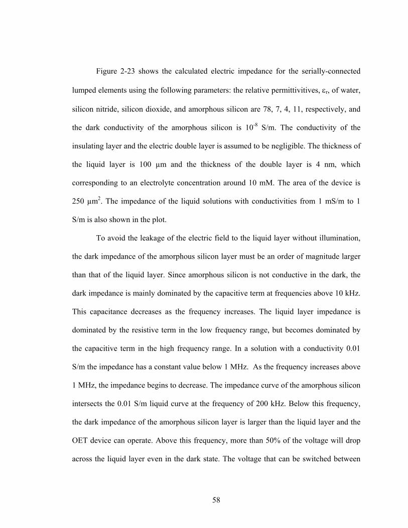
58
Figure 2-23 shows the calculated electric impedance for the serially-connected
lumped elements using the following parameters: the relative permittivitives, εr, of water,
silicon nitride, silicon dioxide, and amorphous silicon are 78, 7, 4, 11, respectively, and
the dark conductivity of the amorphous silicon is 10-8 S/m. The conductivity of the
insulating layer and the electric double layer is assumed to be negligible. The thickness of
the liquid layer is 100 µm and the thickness of the double layer is 4 nm, which
corresponding to an electrolyte concentration around 10 mM. The area of the device is
250 µm2. The impedance of the liquid solutions with conductivities from 1 mS/m to 1
S/m is also shown in the plot.
To avoid the leakage of the electric field to the liquid layer without illumination,
the dark impedance of the amorphous silicon layer must be an order of magnitude larger
than that of the liquid layer. Since amorphous silicon is not conductive in the dark, the
dark impedance is mainly dominated by the capacitive term at frequencies above 10 kHz.
This capacitance decreases as the frequency increases. The liquid layer impedance is
dominated by the resistive term in the low frequency range, but becomes dominated by
the capacitive term in the high frequency range. In a solution with a conductivity 0.01
S/m the impedance has a constant value below 1 MHz. As the frequency increases above
1 MHz, the impedance begins to decrease. The impedance curve of the amorphous silicon
intersects the 0.01 S/m liquid curve at the frequency of 200 kHz. Below this frequency,
the dark impedance of the amorphous silicon layer is larger than the liquid layer and the
OET device can operate. Above this frequency, more than 50% of the voltage will drop
across the liquid layer even in the dark state. The voltage that can be switched between
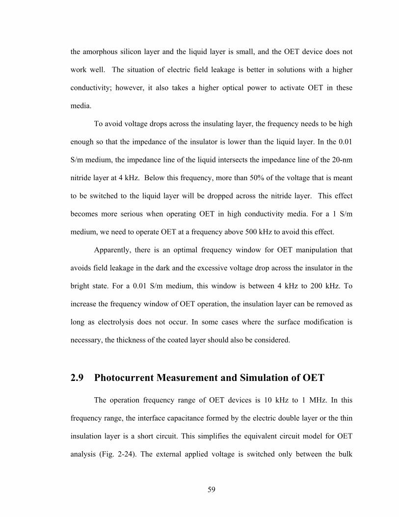
59
the amorphous silicon layer and the liquid layer is small, and the OET device does not
work well. The situation of electric field leakage is better in solutions with a higher
conductivity; however, it also takes a higher optical power to activate OET in these
media.
To avoid voltage drops across the insulating layer, the frequency needs to be high
enough so that the impedance of the insulator is lower than the liquid layer. In the 0.01
S/m medium, the impedance line of the liquid intersects the impedance line of the 20-nm
nitride layer at 4 kHz. Below this frequency, more than 50% of the voltage that is meant
to be switched to the liquid layer will be dropped across the nitride layer. This effect
becomes more serious when operating OET in high conductivity media. For a 1 S/m
medium, we need to operate OET at a frequency above 500 kHz to avoid this effect.
Apparently, there is an optimal frequency window for OET manipulation that
avoids field leakage in the dark and the excessive voltage drop across the insulator in the
bright state. For a 0.01 S/m medium, this window is between 4 kHz to 200 kHz. To
increase the frequency window of OET operation, the insulation layer can be removed as
long as electrolysis does not occur. In some cases where the surface modification is
necessary, the thickness of the coated layer should also be considered.
2.9 Photocurrent Measurement and Simulation of OET
The operation frequency range of OET devices is 10 kHz to 1 MHz. In this
frequency range, the interface capacitance formed by the electric double layer or the thin
insulation layer is a short circuit. This simplifies the equivalent circuit model for OET
analysis (Fig. 2-24). The external applied voltage is switched only between the bulk
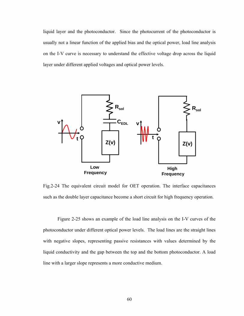
60
liquid layer and the photoconductor. Since the photocurrent of the photoconductor is
usually not a linear function of the applied bias and the optical power, load line analysis
on the I-V curve is necessary to understand the effective voltage drop across the liquid
layer under different applied voltages and optical power levels.
Z(v)
CEDL
Rsol
v
tZ(v)
Rsol
v
t
High Frequency
LowFrequency
Fig.2-24 The equivalent circuit model for OET operation. The interface capacitances
such as the double layer capacitance become a short circuit for high frequency operation.
Figure 2-25 shows an example of the load line analysis on the I-V curves of the
photoconductor under different optical power levels. The load lines are the straight lines
with negative slopes, representing passive resistances with values determined by the
liquid conductivity and the gap between the top and the bottom photoconductor. A load
line with a larger slope represents a more conductive medium.
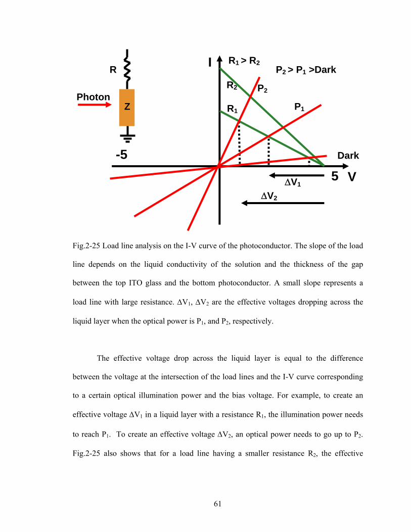
61
Fig.2-25 Load line analysis on the I-V curve of the photoconductor. The slope of the load
line depends on the liquid conductivity of the solution and the thickness of the gap
between the top ITO glass and the bottom photoconductor. A small slope represents a
load line with large resistance. ΔV1, ΔV2 are the effective voltages dropping across the
liquid layer when the optical power is P1, and P2, respectively.
The effective voltage drop across the liquid layer is equal to the difference
between the voltage at the intersection of the load lines and the I-V curve corresponding
to a certain optical illumination power and the bias voltage. For example, to create an
effective voltage ΔV1 in a liquid layer with a resistance R1, the illumination power needs
to reach P1. To create an effective voltage ΔV2, an optical power needs to go up to P2.
Fig.2-25 also shows that for a load line having a smaller resistance R2, the effective
V
I
5-5
P1
P2
Dark
P2 > P1 >Dark
R1
Photon
R
Z
ΔV1
ΔV2
R2
R1 > R2
62
voltage that can be switched to the liquid layer under the same optical power is smaller
than that of the load line having a higher resistance R1.
During OET operation, a signal with a large ac bias and zero dc bias is applied to
provide a sufficient DEP force for particle manipulation. In the load line analysis, this
means that the load line sweeps from the positive bias region to the negative bias region.
No dc bias is applied since the dc bias will be filtered out by the interface capacitance and
will probably create electrolysis at the photoconductor interface.
Electrical characterization of the OET device is challenging since it is operated in
a large signal ac bias. Exact characterization of the electrical properties of the OET
device is difficult since most of the current commercially available equipment such as
impedance analyzers or LCR meters only provide small signal analysis functions. Instead,
we have used some indirect methods to characterize the OET devices.
To measure the I-V curves of the OET devices for load line analysis, we have
adapted a modified OET structure which replaces the interface capacitance with an ohmic
contact electrode as shown in the inset of Fig. 2-26. This does not interfere with
characterization; since OET operates at a high frequency, the interface capacitances
between the liquid and the photoconductor are modeled as short circuits. This adapted
OET structure also has the same multiple layer structure of the original OET device,
except the top nitride layer is replaced by a 50-nm N+ a-Si:H layer and an aluminum layer.
The function of the N+ layers is to reduce the contact resistance between the electrode and
the intrinsic amorphous silicon layer. The thickness of the intrinsic layer is kept the same
as the real OET device. Optical illumination is introduced from the lower ITO glass
surface. Fig. 2-26 shows the I-V curve of this adapted structure under illumination of 51
63
mW/cm2 light intensity. The light source is a 625-nm LED. The data shows that the
photocurrent decays as the illumination time increases. In Fig. 2-27, we plot the
photocurrent at the 5 volt bias is as a function of time. A 38% decay of the photocurrent
has been observed after 80 minutes of illumination. This decay of the photocurrent comes
from the light-induced defect states in the amorphous silicon. The decay of the
photocurrent could affect the OET operation by decreasing the effective voltage drop
across the liquid layer when the light intensity is low. We will show the effect in Chap. 4
when discussing the particle sorting using an integrated virtual optical machine. However,
the decayed photocurrent can be recovered by annealing the device at 150oC for 1 hour
[11]. A load line representing a liquid conductivity of 0.01 S/m is drawn on the I-V
curves to show the effective voltage drop across the liquid layer under this illumination
(Fig. 2-26). Illumination at this light intensity can switch 3V of the applied 5V to the
liquid layer.
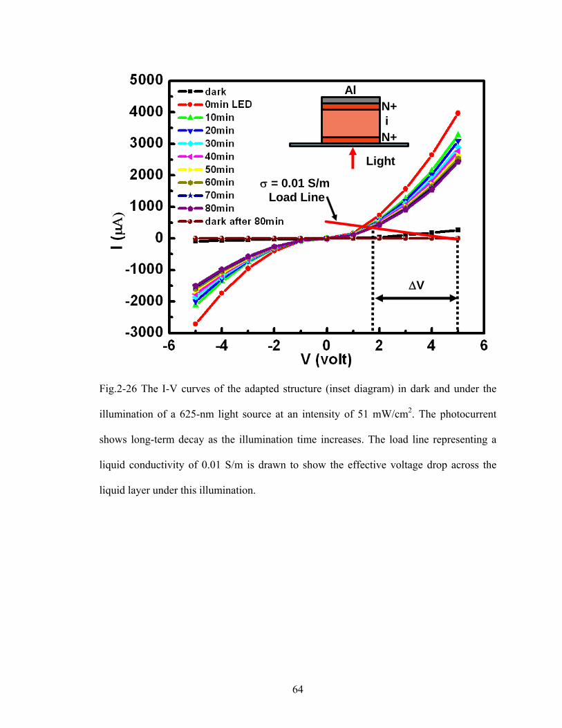
64
Al
N+
N+i
Light
σ = 0.01 S/mLoad Line
ΔV
Fig.2-26 The I-V curves of the adapted structure (inset diagram) in dark and under the
illumination of a 625-nm light source at an intensity of 51 mW/cm2. The photocurrent
shows long-term decay as the illumination time increases. The load line representing a
liquid conductivity of 0.01 S/m is drawn to show the effective voltage drop across the
liquid layer under this illumination.
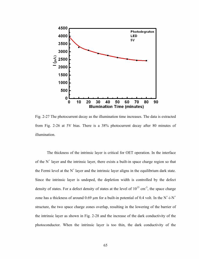
65
Fig. 2-27 The photocurrent decay as the illumination time increases. The data is extracted
from Fig. 2-26 at 5V bias. There is a 38% photocurrent decay after 80 minutes of
illumination.
The thickness of the intrinsic layer is critical for OET operation. In the interface
of the N+ layer and the intrinsic layer, there exists a built-in space charge region so that
the Fermi level at the N+ layer and the intrinsic layer aligns in the equilibrium dark state.
Since the intrinsic layer is undoped, the depletion width is controlled by the defect
density of states. For a defect density of states at the level of 1015 cm-3, the space charge
zone has a thickness of around 0.69 µm for a built-in potential of 0.4 volt. In the N+-i-N+
structure, the two space charge zones overlap, resulting in the lowering of the barrier of
the intrinsic layer as shown in Fig. 2-28 and the increase of the dark conductivity of the
photoconductor. When the intrinsic layer is too thin, the dark conductivity of the
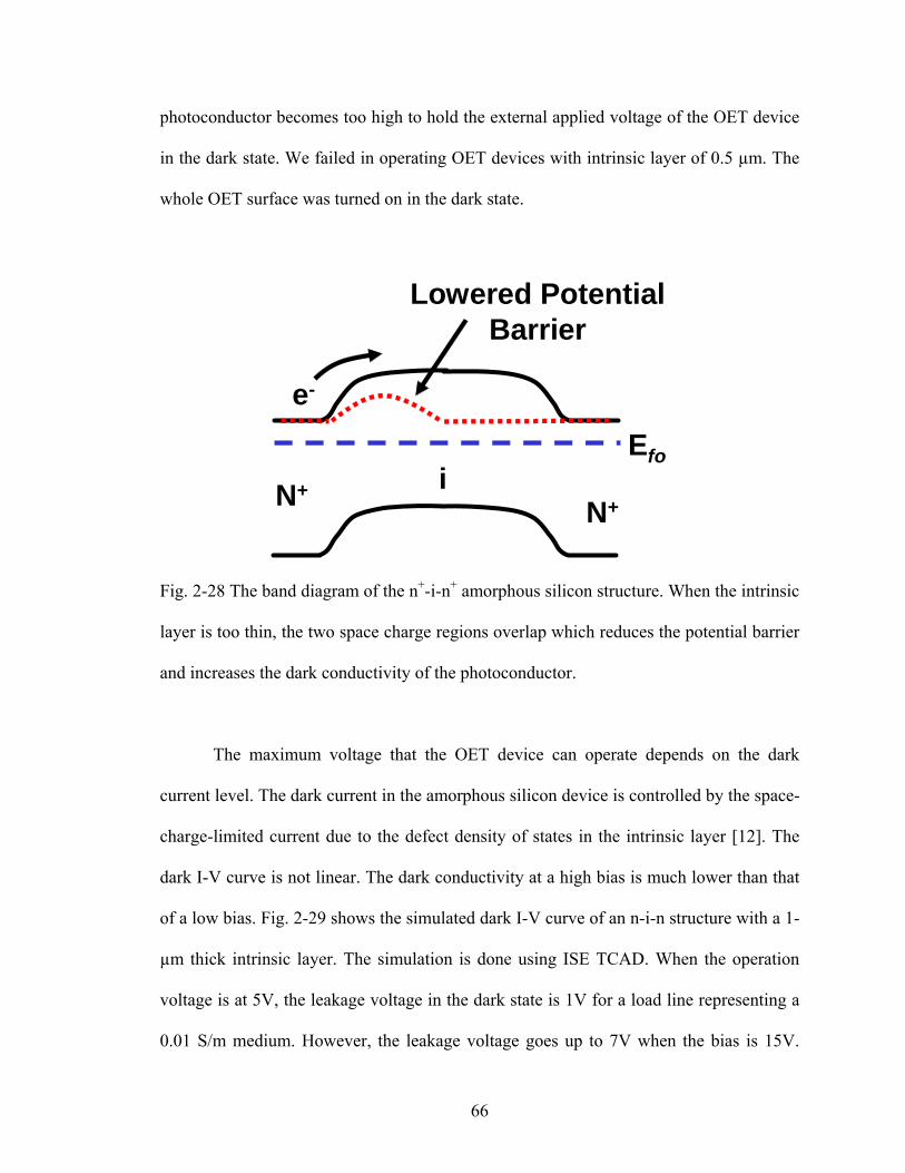
66
photoconductor becomes too high to hold the external applied voltage of the OET device
in the dark state. We failed in operating OET devices with intrinsic layer of 0.5 µm. The
whole OET surface was turned on in the dark state.
Efo
e-
Lowered Potential Barrier
N+N+
i
Fig. 2-28 The band diagram of the n+-i-n+ amorphous silicon structure. When the intrinsic
layer is too thin, the two space charge regions overlap which reduces the potential barrier
and increases the dark conductivity of the photoconductor.
The maximum voltage that the OET device can operate depends on the dark
current level. The dark current in the amorphous silicon device is controlled by the space-
charge-limited current due to the defect density of states in the intrinsic layer [12]. The
dark I-V curve is not linear. The dark conductivity at a high bias is much lower than that
of a low bias. Fig. 2-29 shows the simulated dark I-V curve of an n-i-n structure with a 1-
µm thick intrinsic layer. The simulation is done using ISE TCAD. When the operation
voltage is at 5V, the leakage voltage in the dark state is 1V for a load line representing a
0.01 S/m medium. However, the leakage voltage goes up to 7V when the bias is 15V.
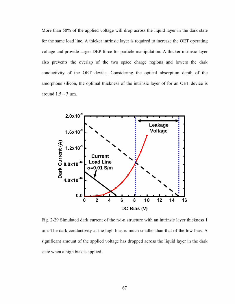
67
More than 50% of the applied voltage will drop across the liquid layer in the dark state
for the same load line. A thicker intrinsic layer is required to increase the OET operating
voltage and provide larger DEP force for particle manipulation. A thicker intrinsic layer
also prevents the overlap of the two space charge regions and lowers the dark
conductivity of the OET device. Considering the optical absorption depth of the
amorphous silicon, the optimal thickness of the intrinsic layer of for an OET device is
around 1.5 ~ 3 µm.
CurrentLoad Lineσ=0.01 S/m
LeakageVoltage
Fig. 2-29 Simulated dark current of the n-i-n structure with an intrinsic layer thickness 1
µm. The dark conductivity at the high bias is much smaller than that of the low bias. A
significant amount of the applied voltage has dropped across the liquid layer in the dark
state when a high bias is applied.
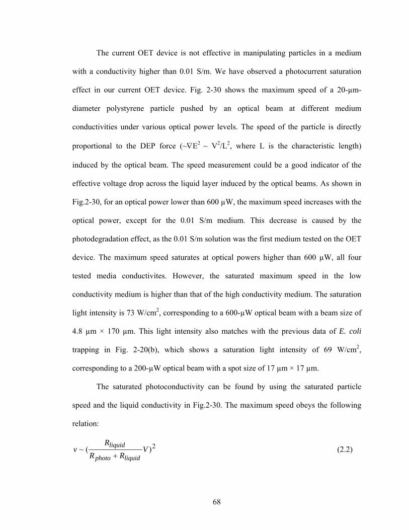
68
The current OET device is not effective in manipulating particles in a medium
with a conductivity higher than 0.01 S/m. We have observed a photocurrent saturation
effect in our current OET device. Fig. 2-30 shows the maximum speed of a 20-µm-
diameter polystyrene particle pushed by an optical beam at different medium
conductivities under various optical power levels. The speed of the particle is directly
proportional to the DEP force (~∇E2 ~ V2/L2, where L is the characteristic length)
induced by the optical beam. The speed measurement could be a good indicator of the
effective voltage drop across the liquid layer induced by the optical beams. As shown in
Fig.2-30, for an optical power lower than 600 µW, the maximum speed increases with the
optical power, except for the 0.01 S/m medium. This decrease is caused by the
photodegradation effect, as the 0.01 S/m solution was the first medium tested on the OET
device. The maximum speed saturates at optical powers higher than 600 µW, all four
tested media conductivites. However, the saturated maximum speed in the low
conductivity medium is higher than that of the high conductivity medium. The saturation
light intensity is 73 W/cm2, corresponding to a 600-µW optical beam with a beam size of
4.8 µm × 170 µm. This light intensity also matches with the previous data of E. coli
trapping in Fig. 2-20(b), which shows a saturation light intensity of 69 W/cm2,
corresponding to a 200-µW optical beam with a spot size of 17 µm × 17 µm.
The saturated photoconductivity can be found by using the saturated particle
speed and the liquid conductivity in Fig.2-30. The maximum speed obeys the following
relation:
2)(~ VRR
Rv
liquidphoto
liquid
+ (2.2)
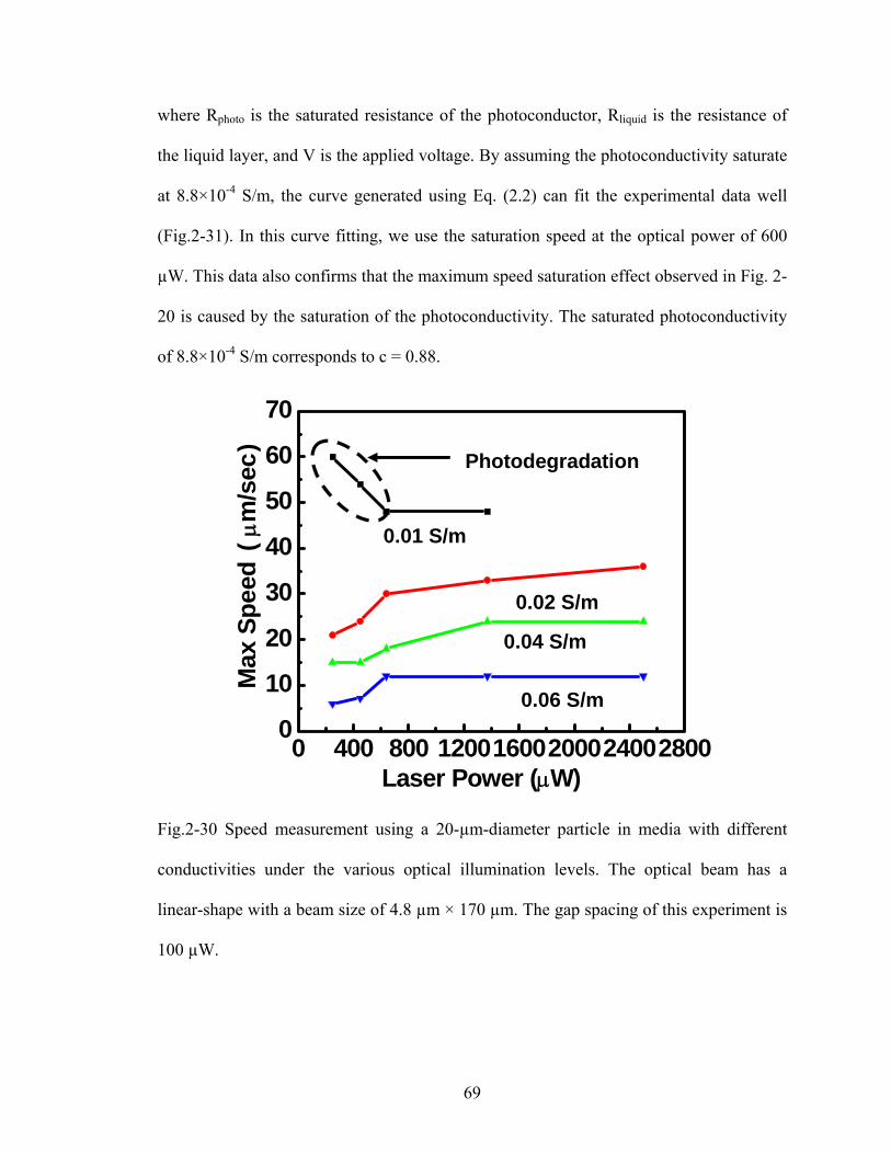
69
where Rphoto is the saturated resistance of the photoconductor, Rliquid is the resistance of
the liquid layer, and V is the applied voltage. By assuming the photoconductivity saturate
at 8.8×10⁻⁴ S/m, the curve generated using Eq. (2.2) can fit the experimental data well
(Fig.2-31). In this curve fitting, we use the saturation speed at the optical power of 600
µW. This data also confirms that the maximum speed saturation effect observed in Fig. 2-
20 is caused by the saturation of the photoconductivity. The saturated photoconductivity
of 8.8×10⁻⁴ S/m corresponds to c = 0.88.
0 400 800 120016002000240028000
10
20
30
40
50
60
70
0.06 S/m
0.04 S/m
0.02 S/m
M
ax S
peed
( μ
m/s
ec)
Laser Power (μW)
0.01 S/m0.01 S/m
0.02 S/m
0.04 S/m
0.06 S/m
Photodegradation
Fig.2-30 Speed measurement using a 20-µm-diameter particle in media with different
conductivities under the various optical illumination levels. The optical beam has a
linear-shape with a beam size of 4.8 µm × 170 µm. The gap spacing of this experiment is
100 µW.
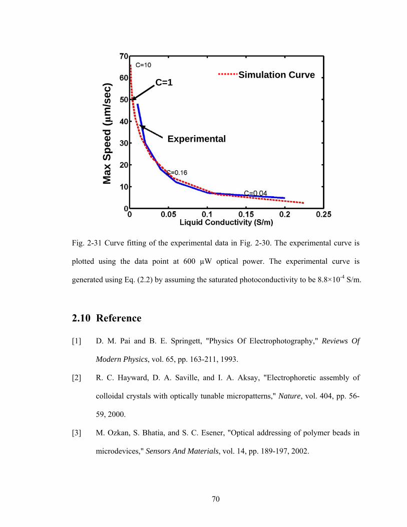
70
Max
Spe
ed (μ
m/s
ec) C=1
Experimental
Simulation Curve
Fig. 2-31 Curve fitting of the experimental data in Fig. 2-30. The experimental curve is
plotted using the data point at 600 µW optical power. The experimental curve is
generated using Eq. (2.2) by assuming the saturated photoconductivity to be 8.8×10⁻⁴ S/m.
2.10 Reference
[1] D. M. Pai and B. E. Springett, "Physics Of Electrophotography," Reviews Of
Modern Physics, vol. 65, pp. 163-211, 1993.
[2] R. C. Hayward, D. A. Saville, and I. A. Aksay, "Electrophoretic assembly of
colloidal crystals with optically tunable micropatterns," Nature, vol. 404, pp. 56-
59, 2000.
[3] M. Ozkan, S. Bhatia, and S. C. Esener, "Optical addressing of polymer beads in
microdevices," Sensors And Materials, vol. 14, pp. 189-197, 2002.
71
[4] S. Wang, Fundamentals of semiconductor theory and device physics. New Jersey:
Prentice Hall, 1989.
[5] R. Schwarz, F. Wang, and M. Reissner, "Fermi-Level Dependence Of The
Ambipolar Diffusion Length In Amorphous-Silicon Thin-Film Transistors,"
Applied Physics Letters, vol. 63, pp. 1083-1085, 1993.
[6] T. Tiedje, C. R. Wronski, B. Abeles, and J. M. Cebulka, "Electron-Transport In
Hydrogenated Amorphous-Silicon - Drift Mobility And Junction Capacitance,"
Solar Cells, vol. 2, pp. 301-318, 1980.
[7] M. J. Madou, Fundamentals of microfabrication. New York: CRC Press, 1997.
[8] R. A. Street, Hydrogenated Amorphous Silicon. New York: Cambridge University
Press, 1991.
[9] J. H. Wei and S. C. Lee, "Electrical and optical properties of implanted
amorphous silicon," Journal Of Applied Physics, vol. 76, pp. 1033-1040, 1993.
[10] S. M. Sze, Physics of Semiconductor Devices, 2 ed. New YorK: John Wiley &
Sons, Inc., 1981.
[11] D. L. Staebler and C. R. Wronski, "Optically Induced Conductivity Changes In
Discharge-Produced Hydrogenated Amorphous-Silicon," Journal Of Applied
Physics, vol. 51, pp. 3262-3268, 1980.
[12] V. Cech, "Modeling of the I-V characteristics in amorphous silicon n(+)-i-n(+)
devices," Journal Of Applied Physics, vol. 88, pp. 5374-5380, 2000.
72
CHAPTER 3
Scanning OET for Microparticle Sorting
3.1. Introduction
The optically-patterned electric field generated on the OET surface can be
configured to trap and transport single or multiple cells in parallel. Such a dynamic
reconfigurable electric field can provide driving forces for sorting particles without the
need for the pumps, channels, and valves used in most of the microfluidic sorters [1-4].
This completely eliminates the need for the fabrication and integration of complex
microfluidic components, adding much flexibility for cell or particle manipulation. In
this chapter, a novel particle sorting mechanism based on a dynamic electric field
patterned by scanning OET will be described. The sorting mechanism is based on the
force balance between the hydrodynamic viscous force and the dynamic light-induced
dielectrophoretic force. Randomly distributed particles with different sizes are sorted out
and positioned in deterministic positions relative to a line-shaped scanning laser beam.
3.2 Sorting Mechanism
Optoelectronic tweezers is a novel mechanism that enables optical patterns to
induce highly non-uniform electric fields on a photoconductive thin film material. The
particles near the non-uniform electric field experience a net force, resulting from the
73
interaction between the electric field and the induced electric dipole of the particles. As
discussed in Chap. 2, DEP force is expressed as [5]
)()](*Re[2 23 EKrF mdep ∇= ωεπ (3.1)
where E is the electric field strength, r is the particle radius, εm is the permittivity of the
surrounding medium, ω is the angular frequency of the applied electric field, and K*(ω)
is the Clausius-Mossotti (CM) factor, which has a value between 1 and -0.5, representing
the polarizability of the particle. This force is very sensitive to the size of the particle (r3)
and the non-uniformity of the field (∇E2). When a line-shaped laser beam scans across
the OET surface, it produces an electric field pattern that moves at the same speed, as
shown in Fig. 3.1. This light-induced electric field pushes particles forward in the OET
device. The relative distance between the moving light beam and the particles is
determined by the balance between the DEP force and the viscous force. Using Stoke’s
Law to estimate the viscous force for a moving particle, we obtain the following
relationship between the particle size and non-uniformity of the field:
)](*Re[3)( 22
ωεηkvCEr
m
==∇ (3.2)
where r is the particle radius and C is a constant determined by the light scanning speed,
v, the real part of the CM factor, and the viscosity, η, and permittivity, εm, of the
surrounding medium. Since the term ∇(E2) is a function of the relative distance between
the particle and the electric field maximum, particles with different sizes will have
different deterministic distances to the center of the scanning laser beam. Based on this
principle, particles with different sizes will be sorted out when the laser beam scans
across the OET surface as shown in Fig. 3-1(c).
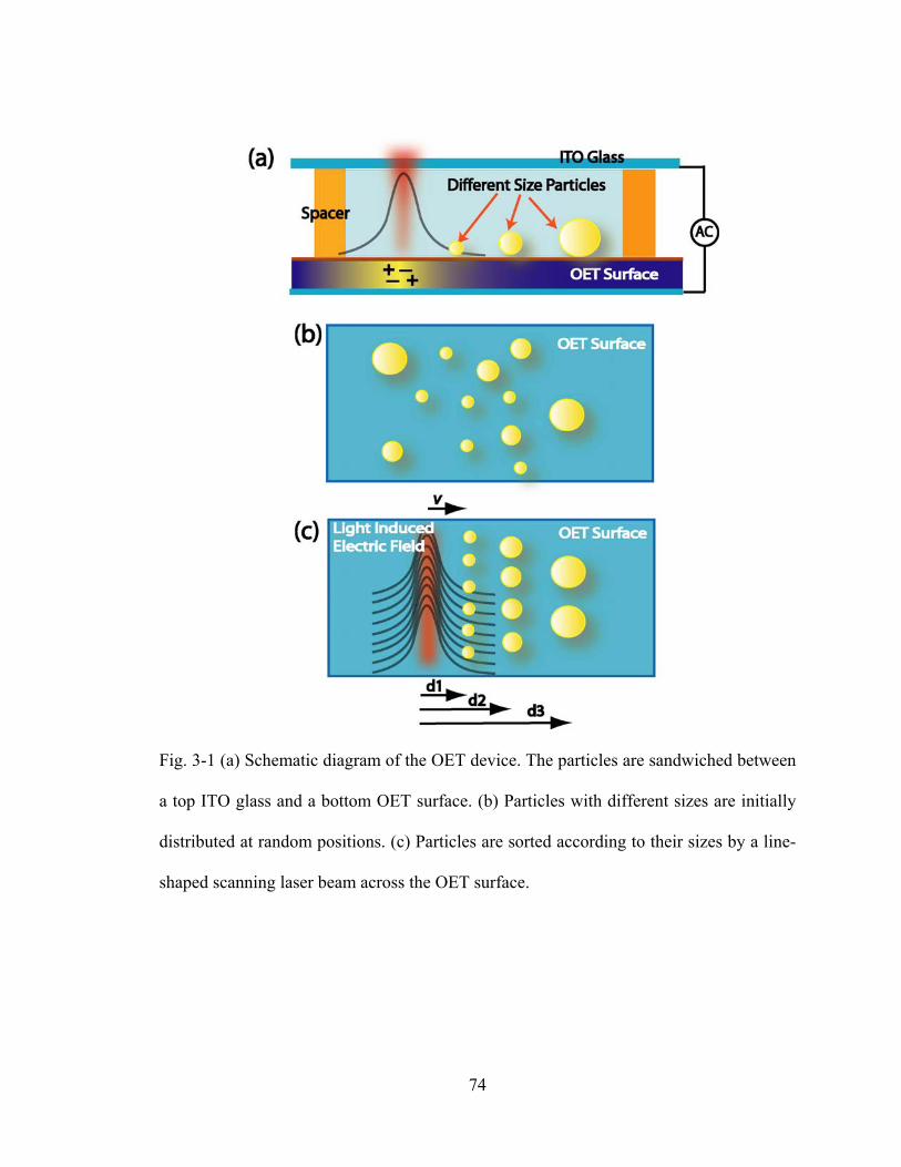
74
Fig. 3-1 (a) Schematic diagram of the OET device. The particles are sandwiched between
a top ITO glass and a bottom OET surface. (b) Particles with different sizes are initially
distributed at random positions. (c) Particles are sorted according to their sizes by a line-
shaped scanning laser beam across the OET surface.
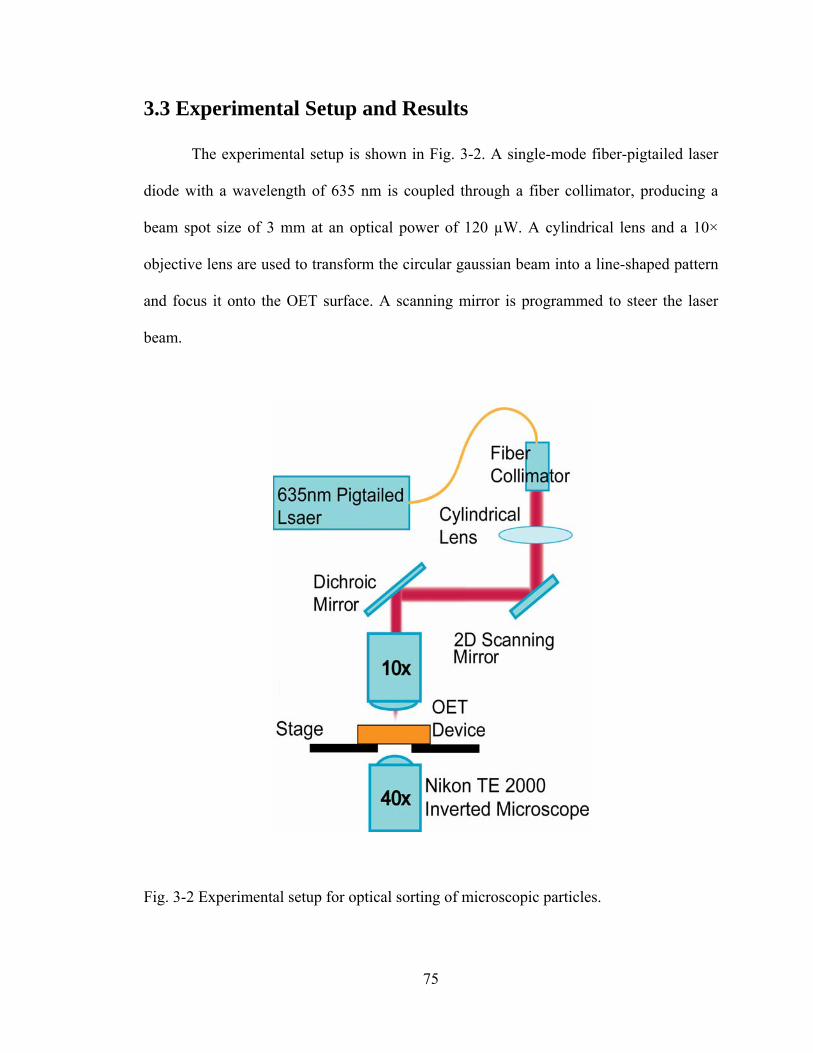
75
3.3 Experimental Setup and Results
The experimental setup is shown in Fig. 3-2. A single-mode fiber-pigtailed laser
diode with a wavelength of 635 nm is coupled through a fiber collimator, producing a
beam spot size of 3 mm at an optical power of 120 µW. A cylindrical lens and a 10×
objective lens are used to transform the circular gaussian beam into a line-shaped pattern
and focus it onto the OET surface. A scanning mirror is programmed to steer the laser
beam.
Fig. 3-2 Experimental setup for optical sorting of microscopic particles.
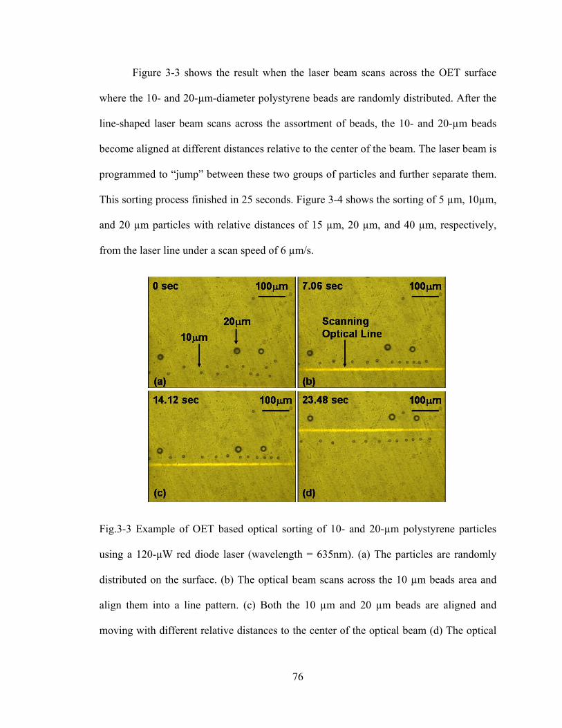
76
Figure 3-3 shows the result when the laser beam scans across the OET surface
where the 10- and 20-µm-diameter polystyrene beads are randomly distributed. After the
line-shaped laser beam scans across the assortment of beads, the 10- and 20-µm beads
become aligned at different distances relative to the center of the beam. The laser beam is
programmed to “jump” between these two groups of particles and further separate them.
This sorting process finished in 25 seconds. Figure 3-4 shows the sorting of 5 µm, 10µm,
and 20 µm particles with relative distances of 15 µm, 20 µm, and 40 µm, respectively,
from the laser line under a scan speed of 6 µm/s.
Fig.3-3 Example of OET based optical sorting of 10- and 20-µm polystyrene particles
using a 120-μW red diode laser (wavelength = 635nm). (a) The particles are randomly
distributed on the surface. (b) The optical beam scans across the 10 µm beads area and
align them into a line pattern. (c) Both the 10 µm and 20 µm beads are aligned and
moving with different relative distances to the center of the optical beam (d) The optical
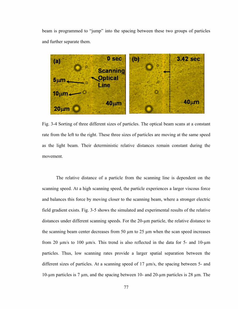
77
beam is programmed to “jump” into the spacing between these two groups of particles
and further separate them.
Fig. 3-4 Sorting of three different sizes of particles. The optical beam scans at a constant
rate from the left to the right. These three sizes of particles are moving at the same speed
as the light beam. Their deterministic relative distances remain constant during the
movement.
The relative distance of a particle from the scanning line is dependent on the
scanning speed. At a high scanning speed, the particle experiences a larger viscous force
and balances this force by moving closer to the scanning beam, where a stronger electric
field gradient exists. Fig. 3-5 shows the simulated and experimental results of the relative
distances under different scanning speeds. For the 20-µm particle, the relative distance to
the scanning beam center decreases from 50 µm to 25 µm when the scan speed increases
from 20 µm/s to 100 µm/s. This trend is also reflected in the data for 5- and 10-µm
particles. Thus, low scanning rates provide a larger spatial separation between the
different sizes of particles. At a scanning speed of 17 µm/s, the spacing between 5- and
10-µm particles is 7 µm, and the spacing between 10- and 20-µm particles is 28 µm. The
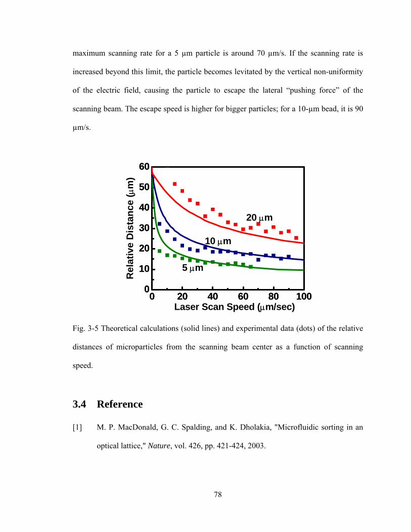
78
maximum scanning rate for a 5 µm particle is around 70 µm/s. If the scanning rate is
increased beyond this limit, the particle becomes levitated by the vertical non-uniformity
of the electric field, causing the particle to escape the lateral “pushing force” of the
scanning beam. The escape speed is higher for bigger particles; for a 10-µm bead, it is 90
µm/s.
0
10
20
30
40
50
60
0 20 40 60 80 1000 20 40 60 80 1000
10
20
30
40
50
60
5 μm
20 μm
Rel
ativ
e D
ista
nce
(μm
)
Laser Scan Speed (μm/sec)
10 μm
Fig. 3-5 Theoretical calculations (solid lines) and experimental data (dots) of the relative
distances of microparticles from the scanning beam center as a function of scanning
speed.
3.4 Reference
[1] M. P. MacDonald, G. C. Spalding, and K. Dholakia, "Microfluidic sorting in an
optical lattice," Nature, vol. 426, pp. 421-424, 2003.
79
[2] P. T. Korda, M. B. Taylor, and D. G. Grier, "Kinetically locked-in colloidal
transport in an array of optical tweezers," Physical Review Letters, vol. 89, 2002.
[3] X. B. Wang, J. Yang, Y. Huang, J. Vykoukal, F. F. Becker, and P. R. C.
Gascoyne, "Cell separation by dielectrophoretic field-flow-fractionation,"
Analytical Chemistry, vol. 72, pp. 832-839, 2000.
[4] P. R. C. Gascoyne, X. B. Wang, Y. Huang, and F. F. Becker, "Dielectrophoretic
separation of cancer cells from blood," Ieee Transactions On Industry
Applications, vol. 33, pp. 670-678, 1997.
[5] T. B. Jones, Electromechanics of particles. New York: Cambridge University
Press, 1995.
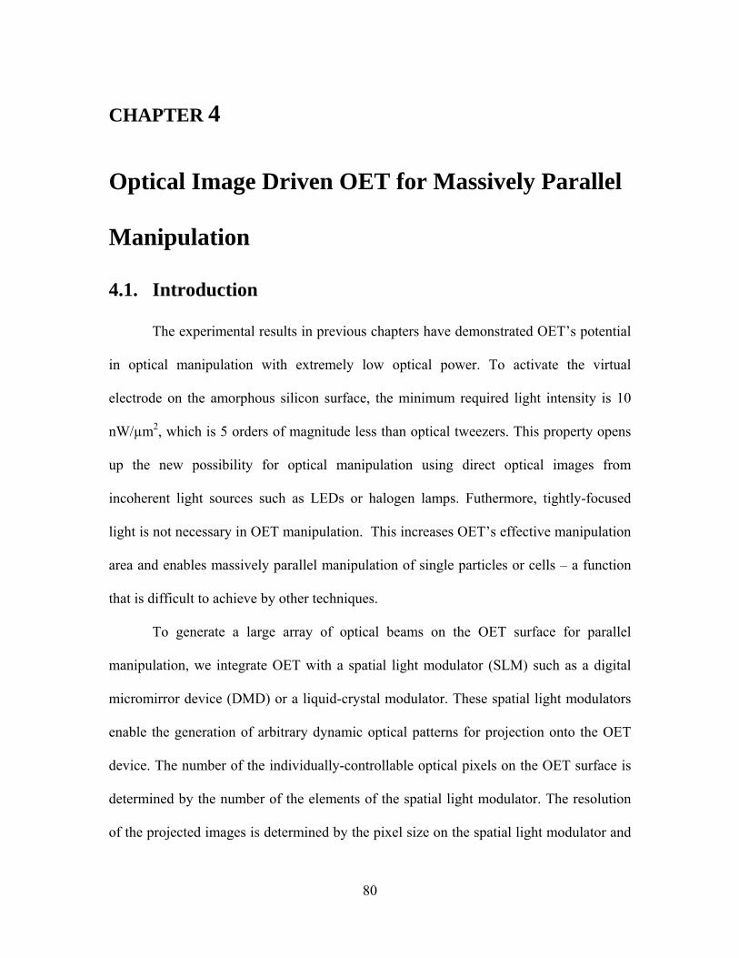
80
CHAPTER 4
Optical Image Driven OET for Massively Parallel
Manipulation
4.1. Introduction
The experimental results in previous chapters have demonstrated OET’s potential
in optical manipulation with extremely low optical power. To activate the virtual
electrode on the amorphous silicon surface, the minimum required light intensity is 10
nW/µm2, which is 5 orders of magnitude less than optical tweezers. This property opens
up the new possibility for optical manipulation using direct optical images from
incoherent light sources such as LEDs or halogen lamps. Futhermore, tightly-focused
light is not necessary in OET manipulation. This increases OET’s effective manipulation
area and enables massively parallel manipulation of single particles or cells – a function
that is difficult to achieve by other techniques.
To generate a large array of optical beams on the OET surface for parallel
manipulation, we integrate OET with a spatial light modulator (SLM) such as a digital
micromirror device (DMD) or a liquid-crystal modulator. These spatial light modulators
enable the generation of arbitrary dynamic optical patterns for projection onto the OET
device. The number of the individually-controllable optical pixels on the OET surface is
determined by the number of the elements of the spatial light modulator. The resolution
of the projected images is determined by the pixel size on the spatial light modulator and
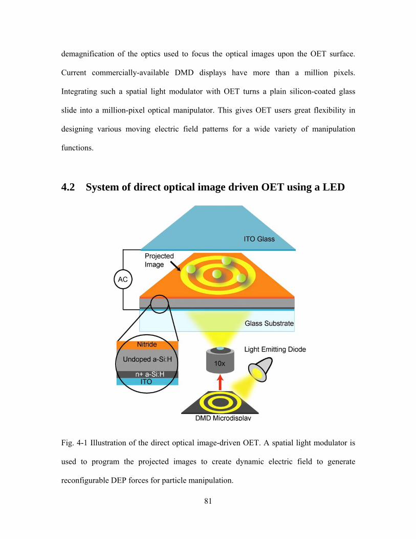
81
demagnification of the optics used to focus the optical images upon the OET surface.
Current commercially-available DMD displays have more than a million pixels.
Integrating such a spatial light modulator with OET turns a plain silicon-coated glass
slide into a million-pixel optical manipulator. This gives OET users great flexibility in
designing various moving electric field patterns for a wide variety of manipulation
functions.
4.2 System of direct optical image driven OET using a LED
Fig. 4-1 Illustration of the direct optical image-driven OET. A spatial light modulator is
used to program the projected images to create dynamic electric field to generate
reconfigurable DEP forces for particle manipulation.
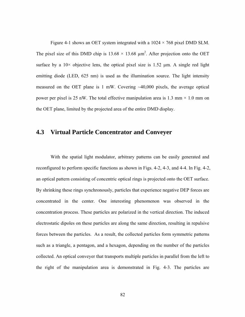
82
Figure 4-1 shows an OET system integrated with a 1024 × 768 pixel DMD SLM.
The pixel size of this DMD chip is 13.68 × 13.68 µm2. After projection onto the OET
surface by a 10× objective lens, the optical pixel size is 1.52 µm. A single red light
emitting diode (LED, 625 nm) is used as the illumination source. The light intensity
measured on the OET plane is 1 mW. Covering ~40,000 pixels, the average optical
power per pixel is 25 nW. The total effective manipulation area is 1.3 mm × 1.0 mm on
the OET plane, limited by the projected area of the entire DMD display.
4.3 Virtual Particle Concentrator and Conveyer
With the spatial light modulator, arbitrary patterns can be easily generated and
reconfigured to perform specific functions as shown in Figs. 4-2, 4-3, and 4-4. In Fig. 4-2,
an optical pattern consisting of concentric optical rings is projected onto the OET surface.
By shrinking these rings synchronously, particles that experience negative DEP forces are
concentrated in the center. One interesting phenomenon was observed in the
concentration process. These particles are polarized in the vertical direction. The induced
electrostatic dipoles on these particles are along the same direction, resulting in repulsive
forces between the particles. As a result, the collected particles form symmetric patterns
such as a triangle, a pentagon, and a hexagon, depending on the number of the particles
collected. An optical conveyer that transports multiple particles in parallel from the left to
the right of the manipulation area is demonstrated in Fig. 4-3. The particles are
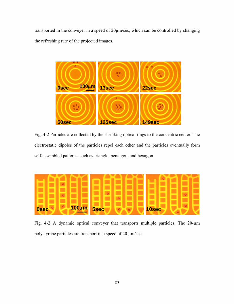
83
transported in the conveyer in a speed of 20µm/sec, which can be controlled by changing
the refreshing rate of the projected images.
Fig. 4-2 Particles are collected by the shrinking optical rings to the concentric center. The
electrostatic dipoles of the particles repel each other and the particles eventually form
self-assembled patterns, such as triangle, pentagon, and hexagon.
0sec 5sec 10sec100μm
Fig. 4-2 A dynamic optical conveyer that transports multiple particles. The 20-µm
polystyrene particles are transport in a speed of 20 µm/sec.
125sec 149sec
0sec 13sec 22sec
50sec
100μm
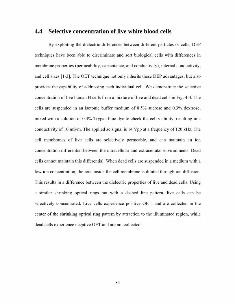
84
4.4 Selective concentration of live white blood cells
By exploiting the dielectric differences between different particles or cells, DEP
techniques have been able to discriminate and sort biological cells with differences in
membrane properties (permeability, capacitance, and conductivity), internal conductivity,
and cell sizes [1-3]. The OET technique not only inherits these DEP advantages, but also
provides the capability of addressing each individual cell. We demonstrate the selective
concentration of live human B cells from a mixture of live and dead cells in Fig. 4-4. The
cells are suspended in an isotonic buffer medium of 8.5% sucrose and 0.3% dextrose,
mixed with a solution of 0.4% Trypan blue dye to check the cell viability, resulting in a
conductivity of 10 mS/m. The applied ac signal is 14 Vpp at a frequency of 120 kHz. The
cell membranes of live cells are selectively permeable, and can maintain an ion
concentration differential between the intracellular and extracellular environments. Dead
cells cannot maintain this differential. When dead cells are suspended in a medium with a
low ion concentration, the ions inside the cell membrane is diluted through ion diffusion.
This results in a difference between the dielectric properties of live and dead cells. Using
a similar shrinking optical rings but with a dashed line pattern, live cells can be
selectively concentrated. Live cells experience positive OET, and are collected in the
center of the shrinking optical ring pattern by attraction to the illuminated region, while
dead cells experience negative OET and are not collected.
85
Fig. 4-4 Selective collection of live cells from a mixture of live and dead cells. The live
cells experience positive OET, trapping them in the bright areas, and pulling the live cells
into the pattern’s center. The dead cells (stained with Trypan blue dye) leak out through
the dark gaps and are not collected.
4.5 Massively Parallel Optical Manipulation of Microscopic
Particles
To demonstrate the high-resolution capabilities of OET, we have created 15,000
DEP traps across an area of 1.3 × 1.0 mm2 as shown in Fig. 4-5(a). The particles are
trapped in the dark area by the induced negative DEP forces, which push the beads into
the non-illuminated regions, where the electric field is weaker. The size of each trap is
optimized to capture a single 4.5-µm diameter polystyrene bead. The pitch between
1 2
3 4
DeadCell
Live Cell
Live Cell
DeadCell
100μm
1 2
3 4
DeadCell
Live Cell
Live Cell
DeadCell
100μm
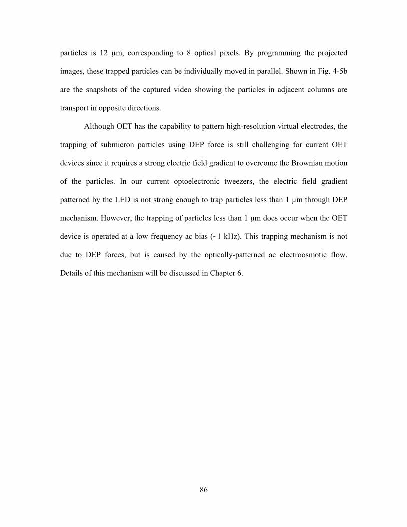
86
particles is 12 µm, corresponding to 8 optical pixels. By programming the projected
images, these trapped particles can be individually moved in parallel. Shown in Fig. 4-5b
are the snapshots of the captured video showing the particles in adjacent columns are
transport in opposite directions.
Although OET has the capability to pattern high-resolution virtual electrodes, the
trapping of submicron particles using DEP force is still challenging for current OET
devices since it requires a strong electric field gradient to overcome the Brownian motion
of the particles. In our current optoelectronic tweezers, the electric field gradient
patterned by the LED is not strong enough to trap particles less than 1 µm through DEP
mechanism. However, the trapping of particles less than 1 μm does occur when the OET
device is operated at a low frequency ac bias (~1 kHz). This trapping mechanism is not
due to DEP forces, but is caused by the optically-patterned ac electroosmotic flow.
Details of this mechanism will be discussed in Chapter 6.
87
Fig. 4-5 Massively parallel manipulation of single particles. (a) 15,000 particle traps are
created across a 1.3 mm × 1.0 mm area. The 4.5 µm-diameter polystyrene beads
experiencing negative DEP forces are trapped in the dark area. Each trap has a diameter
of 4.5 µm, which is adjusted to fit a single particle. (b) Parallel transportation of single
particles. Three snapshots from the captured video show the particle motion in a subset
of the manipulation area. The trapped particles in two adjacent columns move in opposite
directions, as indicated by the blue and yellow arrows.
88
4.6 Integrated Dynamic Optical Patterns for Multi-step
Manipulation
Using direct imaging, sophisticated virtual electrodes can be easily patterned and
reconfigured to create dynamic electric fields for continuous particle manipulation
without the assistance of fluidic flow. Various optical components can be synchronized
and integrated to form a complicated virtual machine for performing multi-step functions.
Fig. 4-6 shows an example of an integrated optical manipulator that combines multiple
functions of optical conveyors, sorters, wedges, and joints. Particles are transported
through different functional areas and recycled in this light-patterned circuit, traveling
through different paths depending on the position of the wedge divider. Particles with
different sizes are fractionated in the vertical z direction as they pass through the sorter
path due to the asymmetric shape of the light-patterned electric fields. The sorting
mechanism is similar to the scanning OET sorting principle that has been discussed in
Chap 3. In Chap 3, we demonstrate one-dimensional sorting using a scanning line-pattern
laser beam, and here, we show an example of two-dimensional sorting. Particles with
different sizes are fractionated in the direction parallel to the direction of movement of
the optical patterns.
After the sorter path, an optical wedge divides and guides the particles into the
two conveyors. The looped optical conveyors can recycle the particles back to the sorter
input to repeat the process. Fig. 4-6(b) and (c) show that the paths of the fractionated
particles can be switched by reconfiguring the tip position of the optical wedge. The
trajectories of the particle movement are highly repeatable and accurately defined even
though the dark area in the conveyer is much larger than the particles. The trace pattern
89
shown in Fig.4-6(b) is the overlap of the loops of the particles traces after 43 cycles
through the optical pattern. Fig. 4-7 shows the distribution of the particle position in the
middle of the sorter (marked by a white bar) after the particles have passed through the
sorter 43 times. The standard variations of trace broadening are 0.5 µm for the 10-µm
bead, and 0.15 µm for the 24-µm bead. As the magnitude of the DEP force is
proportional to the particle volume, the larger particle shows a better confinement in the
optically-patterned DEP cages during transportation. The data shown in Fig.4-7 also
considered the long-term drifting of the average traces due to the metastability of a-Si:H.
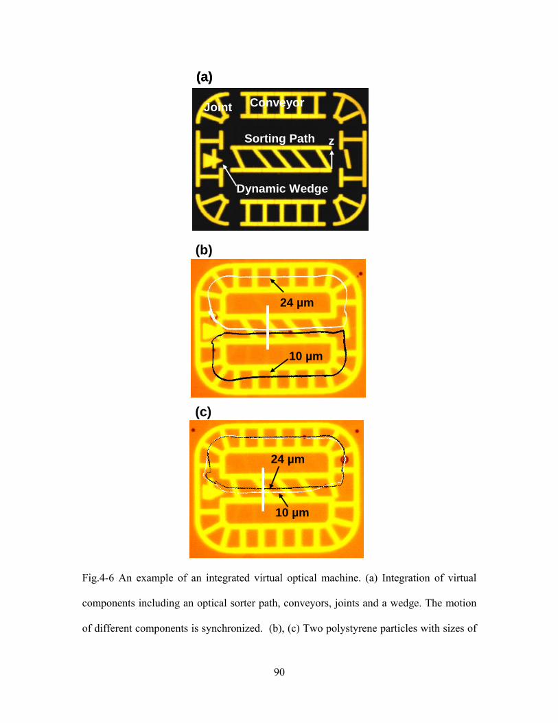
90
Sorting Path
ConveyorJoint
z
Dynamic Wedge
(a)
Sorting Path
ConveyorJoint
z
Dynamic Wedge
(a)
(b)
(c)
24 µm
10 µm
10 µm
24 µm
Fig.4-6 An example of an integrated virtual optical machine. (a) Integration of virtual
components including an optical sorter path, conveyors, joints and a wedge. The motion
of different components is synchronized. (b), (c) Two polystyrene particles with sizes of
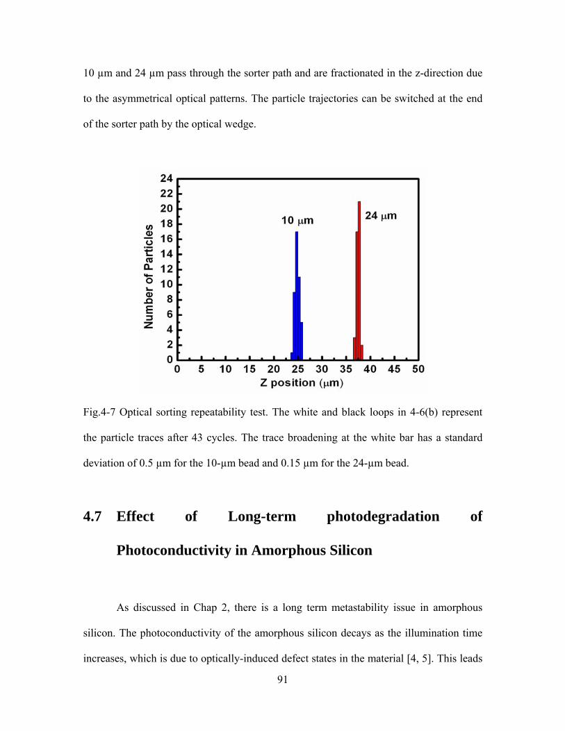
91
10 µm and 24 µm pass through the sorter path and are fractionated in the z-direction due
to the asymmetrical optical patterns. The particle trajectories can be switched at the end
of the sorter path by the optical wedge.
Fig.4-7 Optical sorting repeatability test. The white and black loops in 4-6(b) represent
the particle traces after 43 cycles. The trace broadening at the white bar has a standard
deviation of 0.5 µm for the 10-µm bead and 0.15 µm for the 24-µm bead.
4.7 Effect of Long-term photodegradation of
Photoconductivity in Amorphous Silicon
As discussed in Chap 2, there is a long term metastability issue in amorphous
silicon. The photoconductivity of the amorphous silicon decays as the illumination time
increases, which is due to optically-induced defect states in the material [4, 5]. This leads
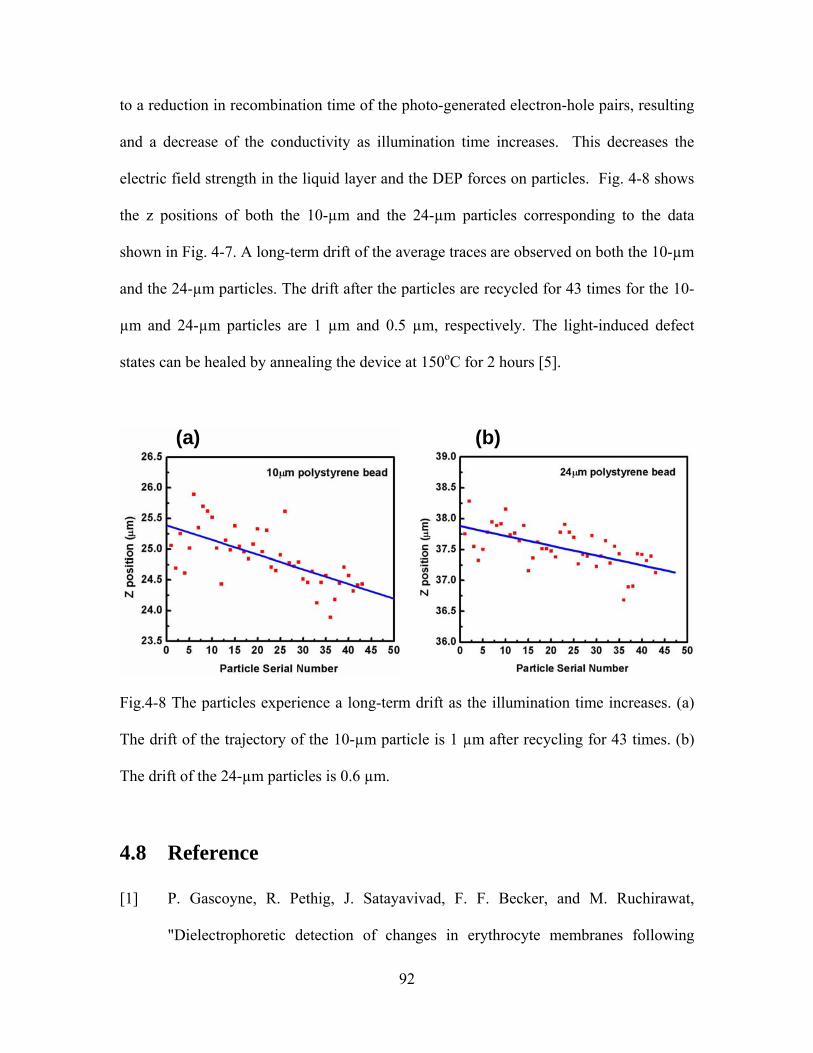
92
to a reduction in recombination time of the photo-generated electron-hole pairs, resulting
and a decrease of the conductivity as illumination time increases. This decreases the
electric field strength in the liquid layer and the DEP forces on particles. Fig. 4-8 shows
the z positions of both the 10-µm and the 24-µm particles corresponding to the data
shown in Fig. 4-7. A long-term drift of the average traces are observed on both the 10-µm
and the 24-µm particles. The drift after the particles are recycled for 43 times for the 10-
µm and 24-µm particles are 1 µm and 0.5 µm, respectively. The light-induced defect
states can be healed by annealing the device at 150oC for 2 hours [5].
(a) (b)
Fig.4-8 The particles experience a long-term drift as the illumination time increases. (a)
The drift of the trajectory of the 10-µm particle is 1 µm after recycling for 43 times. (b)
The drift of the 24-µm particles is 0.6 µm.
4.8 Reference
[1] P. Gascoyne, R. Pethig, J. Satayavivad, F. F. Becker, and M. Ruchirawat,
"Dielectrophoretic detection of changes in erythrocyte membranes following
93
malarial infection," Biochimica Et Biophysica Acta-Biomembranes, vol. 1323, pp.
240-252, 1997.
[2] J. Yang, Y. Huang, X. B. Wang, F. F. Becker, and P. R. C. Gascoyne,
"Differential analysis of human leukocytes by dielectrophoretic field-flow-
fractionation," Biophysical Journal, vol. 78, pp. 2680-2689, 2000.
[3] F. F. Becker, X. B. Wang, Y. Huang, R. Pethig, J. Vykoukal, and P. R. C.
Gascoyne, "Separation Of Human Breast-Cancer Cells From Blood By
Differential Dielectric Affinity," Proceedings Of The National Academy Of
Sciences Of The United States Of America, vol. 92, pp. 860-864, 1995.
[4] V. Nadazdy and M. Zeman, "Origin of charged gap states in a-Si: H and their
evolution during light soaking," Physical Review B, vol. 69, 2004.
[5] D. L. Staebler and C. R. Wronski, "Optically Induced Conductivity Changes In
Discharge-Produced Hydrogenated Amorphous-Silicon," Journal Of Applied
Physics, vol. 51, pp. 3262-3268, 1980.
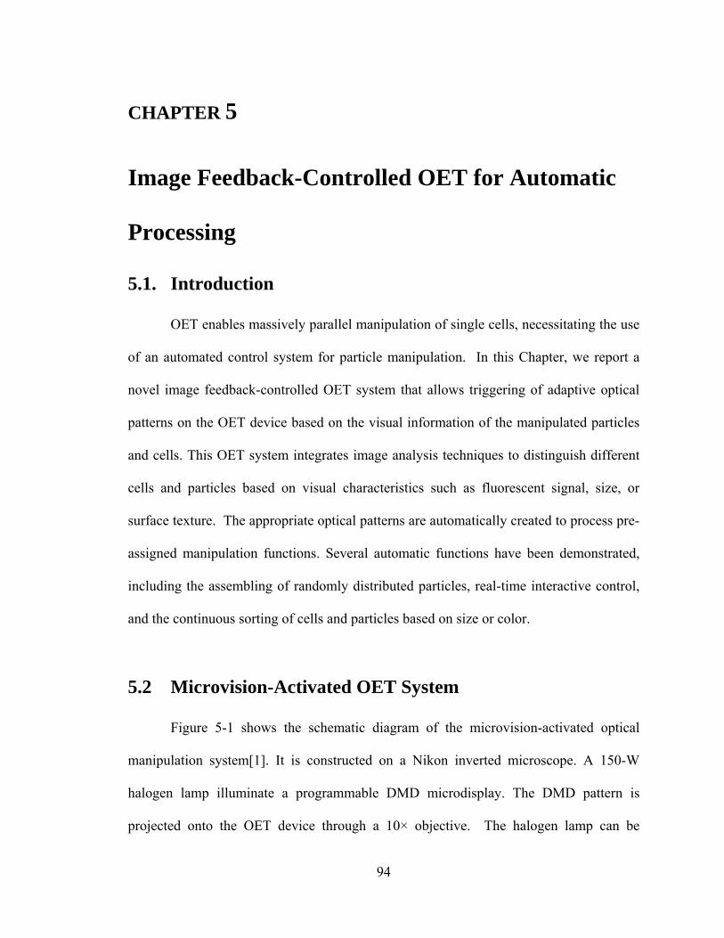
94
CHAPTER 5
Image Feedback-Controlled OET for Automatic
Processing
5.1. Introduction
OET enables massively parallel manipulation of single cells, necessitating the use
of an automated control system for particle manipulation. In this Chapter, we report a
novel image feedback-controlled OET system that allows triggering of adaptive optical
patterns on the OET device based on the visual information of the manipulated particles
and cells. This OET system integrates image analysis techniques to distinguish different
cells and particles based on visual characteristics such as fluorescent signal, size, or
surface texture. The appropriate optical patterns are automatically created to process pre-
assigned manipulation functions. Several automatic functions have been demonstrated,
including the assembling of randomly distributed particles, real-time interactive control,
and the continuous sorting of cells and particles based on size or color.
5.2 Microvision-Activated OET System
Figure 5-1 shows the schematic diagram of the microvision-activated optical
manipulation system[1]. It is constructed on a Nikon inverted microscope. A 150-W
halogen lamp illuminate a programmable DMD microdisplay. The DMD pattern is
projected onto the OET device through a 10× objective. The halogen lamp can be
95
replaced by a single LED if the speed of the particle is not important. The halogen lamp
provides more optical power than the LED, and can more fully turn on the virtual
electrodes for DEP manipulation.
The microscopic image of the particles and cells in the OET device cavity is
captured by a CCD camera through the inverted microscope. A Java-based software
called Processing (http://processing.org/) is used to grab the digital video from the
camera, and analyzes each video frame to acquire the particle information. The
corresponding optical patterns to control particle motion can be automatically generated
by Processing, using customized functions that we wrote in Java. Due to a hardware
interface issue, the controlling software of the DMD kit does not support the real-time
uploading and refreshing of the new optical images onto the DMD display. The
projected images are first stored in an image format (.jpg) and are batch-loaded onto the
DMD control board for display.
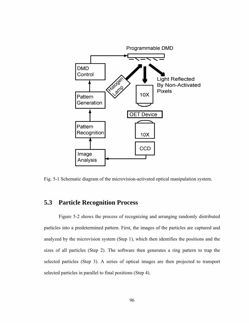
96
Fig. 5-1 Schematic diagram of the microvision-activated optical manipulation system.
5.3 Particle Recognition Process
Figure 5-2 shows the process of recognizing and arranging randomly distributed
particles into a predetermined pattern. First, the images of the particles are captured and
analyzed by the microvision system (Step 1), which then identifies the positions and the
sizes of all particles (Step 2). The software then generates a ring pattern to trap the
selected particles (Step 3). A series of optical images are then projected to transport
selected particles in parallel to final positions (Step 4).
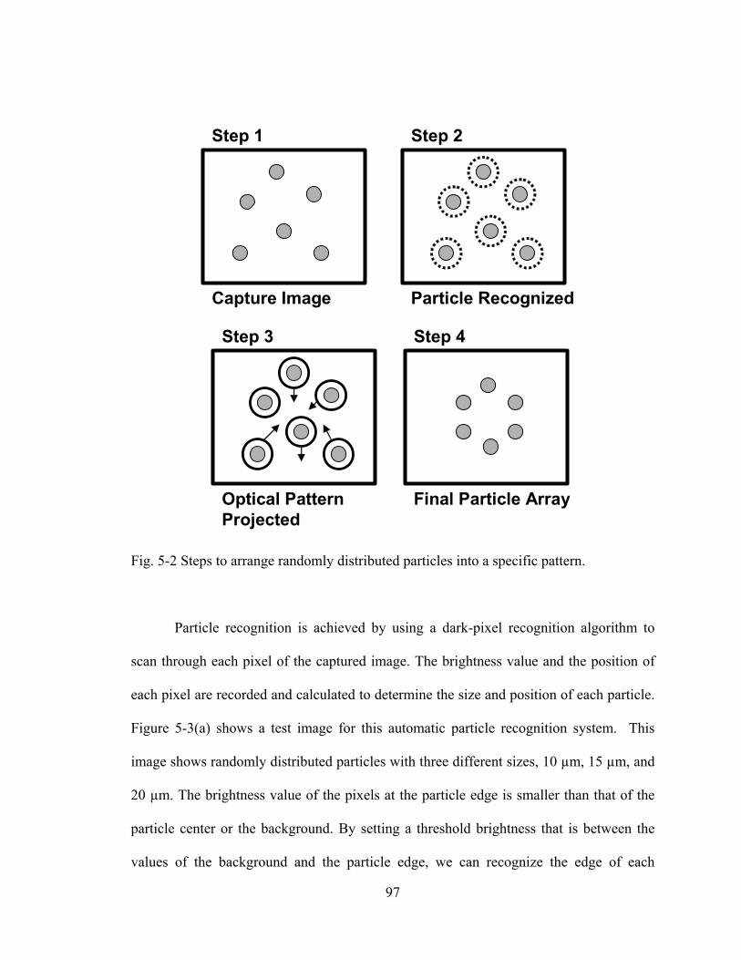
97
Capture Image Particle Recognized
Optical PatternProjected
Final Particle Array
Step 1 Step 2
Step 3 Step 4
Fig. 5-2 Steps to arrange randomly distributed particles into a specific pattern.
Particle recognition is achieved by using a dark-pixel recognition algorithm to
scan through each pixel of the captured image. The brightness value and the position of
each pixel are recorded and calculated to determine the size and position of each particle.
Figure 5-3(a) shows a test image for this automatic particle recognition system. This
image shows randomly distributed particles with three different sizes, 10 µm, 15 µm, and
20 µm. The brightness value of the pixels at the particle edge is smaller than that of the
particle center or the background. By setting a threshold brightness that is between the
values of the background and the particle edge, we can recognize the edge of each
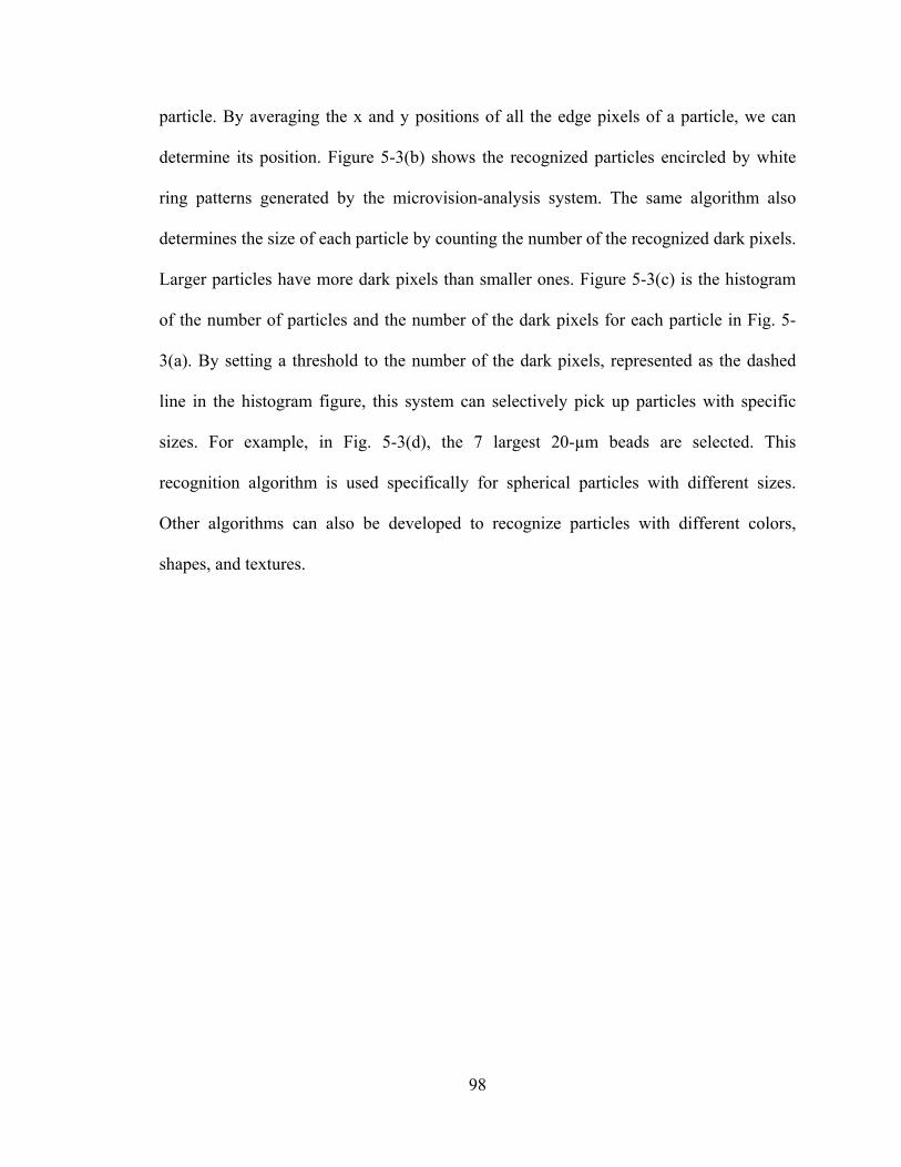
98
particle. By averaging the x and y positions of all the edge pixels of a particle, we can
determine its position. Figure 5-3(b) shows the recognized particles encircled by white
ring patterns generated by the microvision-analysis system. The same algorithm also
determines the size of each particle by counting the number of the recognized dark pixels.
Larger particles have more dark pixels than smaller ones. Figure 5-3(c) is the histogram
of the number of particles and the number of the dark pixels for each particle in Fig. 5-
3(a). By setting a threshold to the number of the dark pixels, represented as the dashed
line in the histogram figure, this system can selectively pick up particles with specific
sizes. For example, in Fig. 5-3(d), the 7 largest 20-µm beads are selected. This
recognition algorithm is used specifically for spherical particles with different sizes.
Other algorithms can also be developed to recognize particles with different colors,
shapes, and textures.
99
Fig. 5-3 (a) Test image for particle recognition. Polystyrene particles with three different
sizes - 10 µm, 15 µm, and 20 µm, are mixed and randomly distributed. (b) The
microvision system recognized the position of each particle and projected a ring marker
around each particle. (c) A histogram of the number of particles and the number of the
dark recognized pixels of the test image. (d) By setting a threshold number of the dark
pixels, the largest particles are selected.
20 µm
15 µm
10 µm
(a) (b)
(c) (d)
100
5.4 Automatic Generation of Optical Patterns for Functional
Manipulation
In this experiment, the OET device is operated in the negative DEP mode, which
repels the particles from strong electric field areas. To trap a single particle with negative
DEP force, we create an optical ring pattern to form a virtual DEP cage that only allows a
single particle to be trapped inside the ring (Fig. 5-4). In the static state, the trapped
particle is focused at the center of the ring pattern, at the location of the minimum electric
field. When the optical ring moves, the trapped particle also moves in the same direction,
but its position deviates from the center of the ring, causing the DEP force to push the
particle back to the center trap. The distance of deviation from the center of the ring is
dependent on how fast the particle moves. If the optical ring moves too fast, the particle
can escape the optical ring, as the DEP restoring force is not strong enough to hold the
particle. The escape velocity of a 20-µm particle is 40 µm/s in this system by using ring-
pattern with line width of 20 µm and light intensity ~ 100 nW/µm2. To trap a particle
with a smaller size, a smaller optical ring would be required, ensuring that only a single
particle can reside in the ring.
Once the particle positions are recognized, the software generates the ring patterns
and calculates the trajectories for all the particles to form a predetermined pattern. These
optical patterns are stored as image files and are batch loaded to the DMD control
software. This process is shown in Fig. 5-5(a). The image of the randomly distributed
particles was scanned vertically from left to right. The first six particles were identified
and trapped by the OET (0 sec). The trapped particles were transported by moving the
ring traps, and reached the hexagonal configuration in 12 seconds. Figures 5-5(b) and 5-
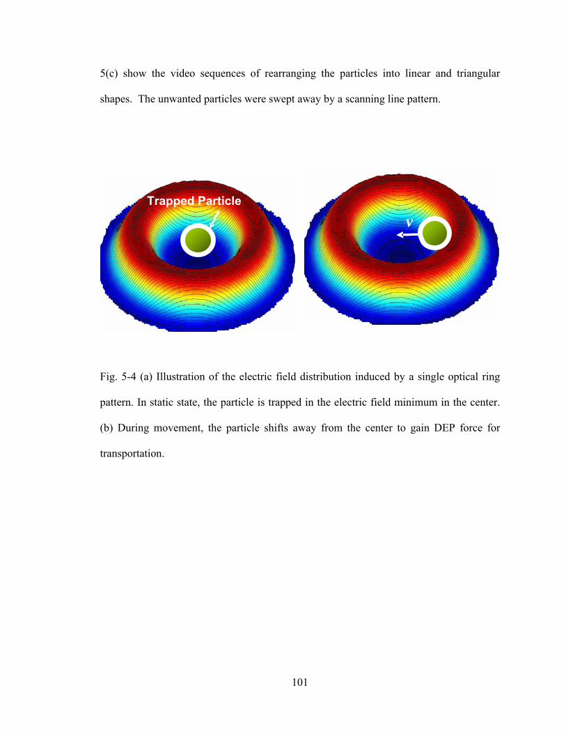
101
5(c) show the video sequences of rearranging the particles into linear and triangular
shapes. The unwanted particles were swept away by a scanning line pattern.
Fig. 5-4 (a) Illustration of the electric field distribution induced by a single optical ring
pattern. In static state, the particle is trapped in the electric field minimum in the center.
(b) During movement, the particle shifts away from the center to gain DEP force for
transportation.
Trapped Particle
v
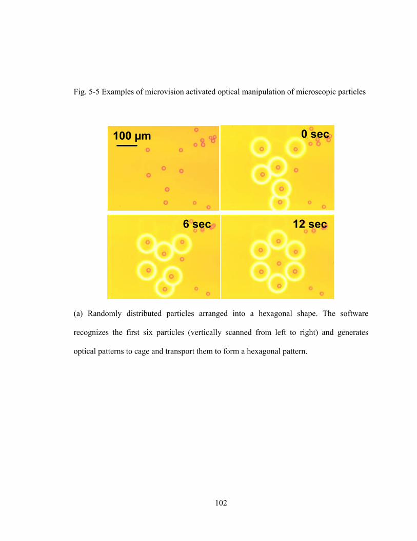
102
Fig. 5-5 Examples of microvision activated optical manipulation of microscopic particles
0 sec
6 sec 12 sec
100 µm
(a) Randomly distributed particles arranged into a hexagonal shape. The software
recognizes the first six particles (vertically scanned from left to right) and generates
optical patterns to cage and transport them to form a hexagonal pattern.
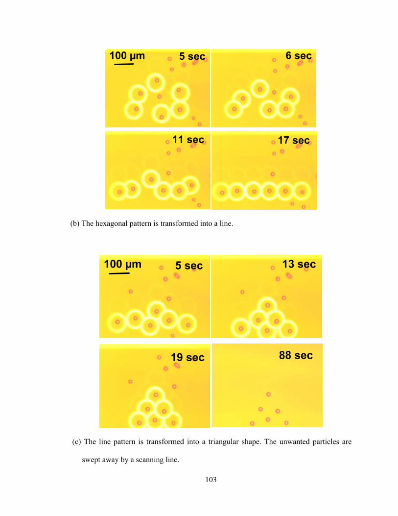
103
5 sec 6 sec
11 sec 17 sec
100 µm
(b) The hexagonal pattern is transformed into a line.
5 sec 13 sec
19 sec
100 µm
88 sec
(c) The line pattern is transformed into a triangular shape. The unwanted particles are
swept away by a scanning line.
104
5.5 Continuous Sorting of Particles and Cells Based on Size
and Color
In the previous section, we used a DMD to pattern the projected images on the
OET device. Although the DMD provides sharp, high-resolution images, loading
refreshed images to the DMD controller takes a few minutes, which is the rate-limiting
step of our current system. Real-time control would require a DMD controller with much
faster refresh rate.
In this section, we use a liquid crystal spatial light modulator (LC-SLM) to create
the optical manipulation patterns. The control interface of the LC-SLM allows for the
real-time refreshing of optical images at a rate of 5 frames per second. With this
capability, we are able to acheive a continuous automatic optical sorting of cells and
particles based on size and color [2].
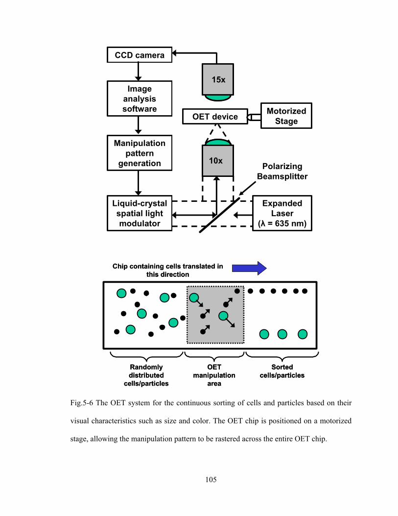
105
OET device
CCD camera
Image analysis software
Manipulation pattern
generation
Expanded Laser
(λ = 635 nm)
Liquid-crystal spatial light modulator
Polarizing Beamsplitter
10x
15x
Motorized Stage
OET manipulation
area
Sorted cells/particles
Randomly distributed
cells/particles
Chip containing cells translated in this direction
OET manipulation
area
Sorted cells/particles
Randomly distributed
cells/particles
Chip containing cells translated in this direction
Fig.5-6 The OET system for the continuous sorting of cells and particles based on their
visual characteristics such as size and color. The OET chip is positioned on a motorized
stage, allowing the manipulation pattern to be rastered across the entire OET chip.
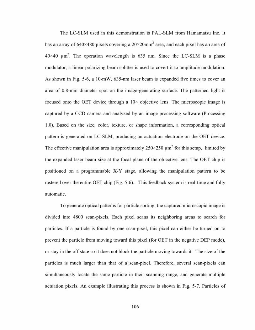
106
The LC-SLM used in this demonstration is PAL-SLM from Hamamatsu Inc. It
has an array of 640×480 pixels covering a 20×20mm2 area, and each pixel has an area of
40×40 µm2. The operation wavelength is 635 nm. Since the LC-SLM is a phase
modulator, a linear polarizing beam splitter is used to covert it to amplitude modulation.
As shown in Fig. 5-6, a 10-mW, 635-nm laser beam is expanded five times to cover an
area of 0.8-mm diameter spot on the image-generating surface. The patterned light is
focused onto the OET device through a 10× objective lens. The microscopic image is
captured by a CCD camera and analyzed by an image processing software (Processing
1.0). Based on the size, color, texture, or shape information, a corresponding optical
pattern is generated on LC-SLM, producing an actuation electrode on the OET device.
The effective manipulation area is approximately 250×250 µm2 for this setup, limited by
the expanded laser beam size at the focal plane of the objective lens. The OET chip is
positioned on a programmable X-Y stage, allowing the manipulation pattern to be
rastered over the entire OET chip (Fig. 5-6). This feedback system is real-time and fully
automatic.
To generate optical patterns for particle sorting, the captured microscopic image is
divided into 4800 scan-pixels. Each pixel scans its neighboring areas to search for
particles. If a particle is found by one scan-pixel, this pixel can either be turned on to
prevent the particle from moving toward this pixel (for OET in the negative DEP mode),
or stay in the off state so it does not block the particle moving towards it. The size of the
particles is much larger than that of a scan-pixel. Therefore, several scan-pixels can
simultaneously locate the same particle in their scanning range, and generate multiple
actuation pixels. An example illustrating this process is shown in Fig. 5-7. Particles of
107
different sizes enter the OET manipulation zone from the bottom. The goal of the sorting
is to collect the large particles on the left side of the screen, and the small particles on the
right side. In the vicinity of the large particle, we see that a scan-pixel has located the
particle on right edge of the pixel. The scan-pixel has turned on to push the particle
towards the left. The scan-pixels to left of the particle have also detected the particle, but
stay in the off state to allow the particle to move to the left. For small particles, the
criteria of the scan-pixels reverse, pushing the small particles to the right. Several pixels
can turn on together to induce DEP forces on a single particle.
onon off
off
Particle moving in
Fig.5-7 The illustration of the algorithm applied to generate optical patterns for particle
sorting. The microscopic image is divided into 4800 scan-pixels. Each pixel scans its
neighboring area searching for particles. Once a particle is found, the pixel can be turned
on or off depending on its relative position to the detected particle and the programmed
criteria for particle.
108
Figure 5-8 shows the test image and the generated optical pattern for projection
onto the OET surface. In Fig. 5-8(a), there are 7 particles. The scan-pixels detect the
presence of the particles, and the scan pixels on the left side of particles (marked by black
dots on the test image) turn on the corresponding pixels of the spatial light modulator,
creating a projected pattern as shown in Fig. 5-8(b). When the optical pattern is projected
onto the OET surface, the bright pixels will map to the marked pixels on the test image.
The number of the scan-pixels can be increased to control smaller particles. Using
a 15× objective lens, a 4800-pixel resolution works well for particles with diameters
larger than 5 µm. To manipulate particles smaller than 5 µm, an objective lens with a
higher magnification can be used, but the effective manipulation area is reduced.
Testing Image Projected Pattern(a) (b)
Fig. 5-8 Testing of the optical pattern generation algorithm for continuous particle sorting.
Figure 5-9 demonstrates a particle sorting function based on size. The OET chip is
programmed to move the particles as they enter from the left side of the manipulation
zone. The larger particles (20 µm) are pushed to the bottom of the image, while the
smaller particles (15 µm) are pushed to the top of the image by the light-induced negative
109
DEP forces. The trajectories of the particles are recorded and plotted in Fig. 5-9(c). The
particles enter the manipulation zone at random positions in the y direction. After they
passed through the 250-µm-wide manipulation zone, the 20- and 15-µm particles are
clearly separated.
100 µm
x
y
(a) (b)
(c)
Fig. 5-9 (a)(b) Continuous particle sorting on 15- and 20-µm-diameter polystyrene beads.
The dashed lines show the position of the optical guiding bars. (c) Trajectories of the
beads entering the active area from the left of the image.
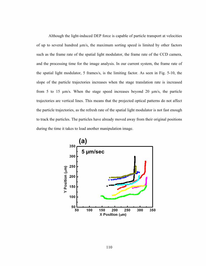
110
Although the light-induced DEP force is capable of particle transport at velocities
of up to several hundred µm/s, the maximum sorting speed is limited by other factors
such as the frame rate of the spatial light modulator, the frame rate of the CCD camera,
and the processing time for the image analysis. In our current system, the frame rate of
the spatial light modulator, 5 frames/s, is the limiting factor. As seen in Fig. 5-10, the
slope of the particle trajectories increases when the stage translation rate is increased
from 5 to 15 µm/s. When the stage speed increases beyond 20 µm/s, the particle
trajectories are vertical lines. This means that the projected optical patterns do not affect
the particle trajectories, as the refresh rate of the spatial light modulator is not fast enough
to track the particles. The particles have already moved away from their original positions
during the time it takes to load another manipulation image.
5 µm/sec
(a)
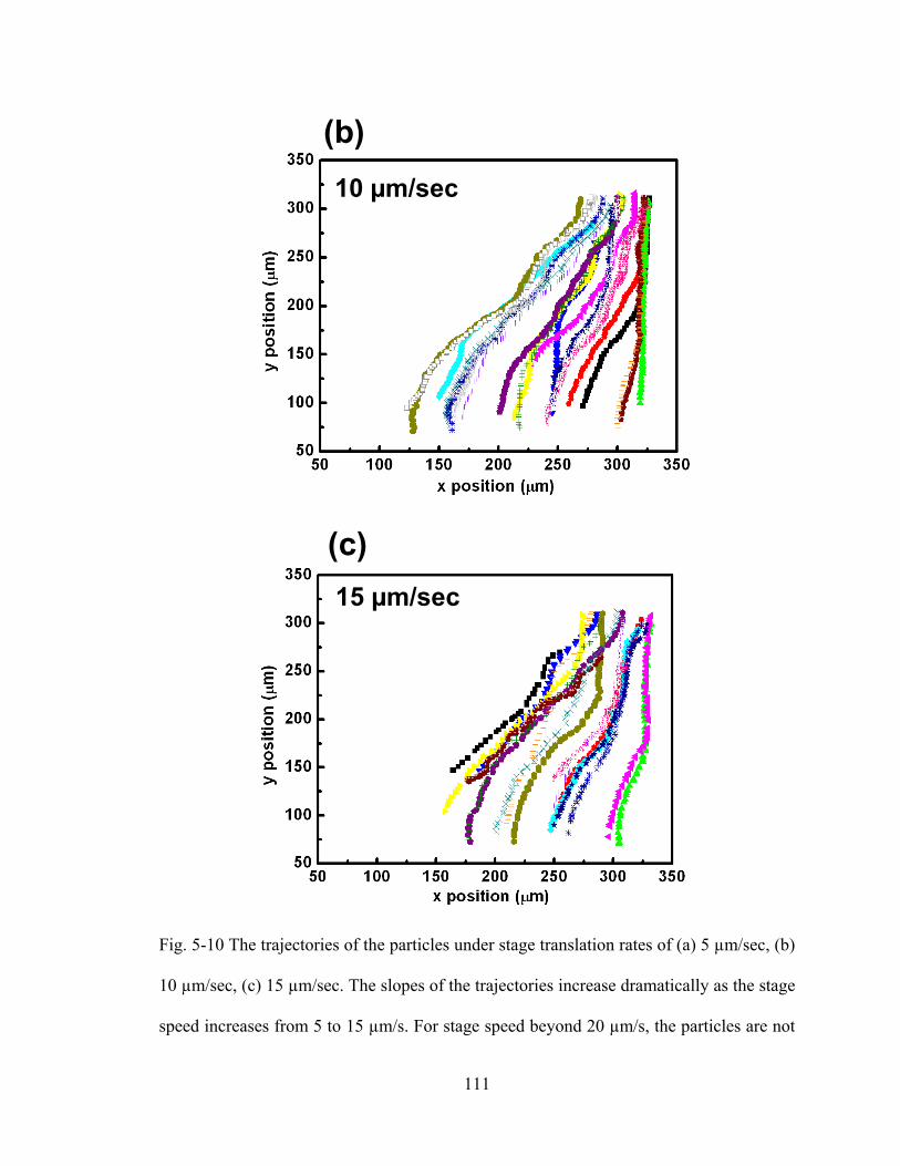
111
10 µm/sec
(b)
15 µm/sec
(c)
Fig. 5-10 The trajectories of the particles under stage translation rates of (a) 5 µm/sec, (b)
10 µm/sec, (c) 15 µm/sec. The slopes of the trajectories increase dramatically as the stage
speed increases from 5 to 15 µm/s. For stage speed beyond 20 µm/s, the particles are not
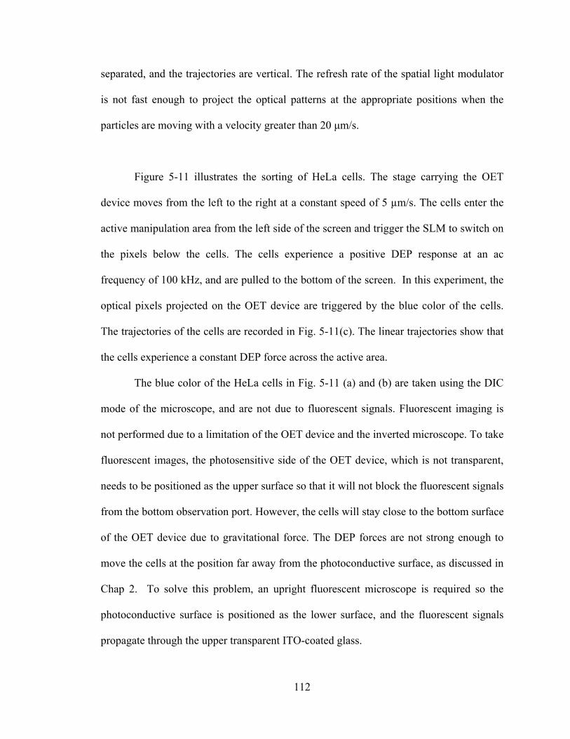
112
separated, and the trajectories are vertical. The refresh rate of the spatial light modulator
is not fast enough to project the optical patterns at the appropriate positions when the
particles are moving with a velocity greater than 20 μm/s.
Figure 5-11 illustrates the sorting of HeLa cells. The stage carrying the OET
device moves from the left to the right at a constant speed of 5 µm/s. The cells enter the
active manipulation area from the left side of the screen and trigger the SLM to switch on
the pixels below the cells. The cells experience a positive DEP response at an ac
frequency of 100 kHz, and are pulled to the bottom of the screen. In this experiment, the
optical pixels projected on the OET device are triggered by the blue color of the cells.
The trajectories of the cells are recorded in Fig. 5-11(c). The linear trajectories show that
the cells experience a constant DEP force across the active area.
The blue color of the HeLa cells in Fig. 5-11 (a) and (b) are taken using the DIC
mode of the microscope, and are not due to fluorescent signals. Fluorescent imaging is
not performed due to a limitation of the OET device and the inverted microscope. To take
fluorescent images, the photosensitive side of the OET device, which is not transparent,
needs to be positioned as the upper surface so that it will not block the fluorescent signals
from the bottom observation port. However, the cells will stay close to the bottom surface
of the OET device due to gravitational force. The DEP forces are not strong enough to
move the cells at the position far away from the photoconductive surface, as discussed in
Chap 2. To solve this problem, an upright fluorescent microscope is required so the
photoconductive surface is positioned as the lower surface, and the fluorescent signals
propagate through the upper transparent ITO-coated glass.
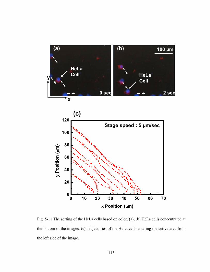
113
2 sec
HeLaCell HeLa
Cell
0 sec
100 µm
2 sec
HeLaCell HeLa
Cell
0 sec
100 µm
x
y
(a) (b)
Stage speed : 5 µm/sec
(c)
Fig. 5-11 The sorting of the HeLa cells based on color. (a), (b) HeLa cells concentrated at
the bottom of the images. (c) Trajectories of the HeLa cells entering the active area from
the left side of the image.
114
5.6. Reference
[1] P. Y. Chiou, A. T. Ohta, and M. C. Wu, "Microvision activated optical
manipulation on microscopic particles," in Proceedings of IEEE Seventeenth
Annual International Conference on Micro Electro Mechanical Systems, pp. 682-
685, 2005.
[2] P. Y. Chiou, A. T. Ohta, and M. C. Wu, "Continuous optical sorting of HeLa cells
and microparticles using optoelectronic tweezers," in Proceedings of IEEE/LEOS
International Conference on Optical MEMS and Their Applications (OMEMS'
05), pp. 83-84, 2005.
115
CHAPTER 6
LIGHT-PATTERNED AC ELECTROOSMOSIS FOR
NANOPARTICLE MANIPULATION
6.1. Introduction
During OET manipulation, an abnormal motion of particles was observed in the
low ac frequency regime, which cannot be explained by DEP forces. This phenomenon
was also observed in many DEP experiments using patterned metal electrodes [1, 2]. A
recently proposed theory has attributed it to the coupling of the tangential component of
the electric field with the surface double layer charges on the electrodes, which creates a
coulomb force at the liquid and electrode interface that drives fluidic flow [3-6]. This ac
electrokinetic mechanism is called ac electroosmosis, and has been introduced in Chap. 1.
In OET manipulation, the majority of the applied voltage should drop across the
liquid layer, creating an electric field gradient and generating DEP forces. However, at
low ac frequencies, the electrical impedance of the electric double layer becomes
significant and compets with that of the bulk liquid layer (Fig. 6-1). This results in a
significant voltage drop across the double layer, charging accumulation at the surface of
the light-patterned virtual electrode.
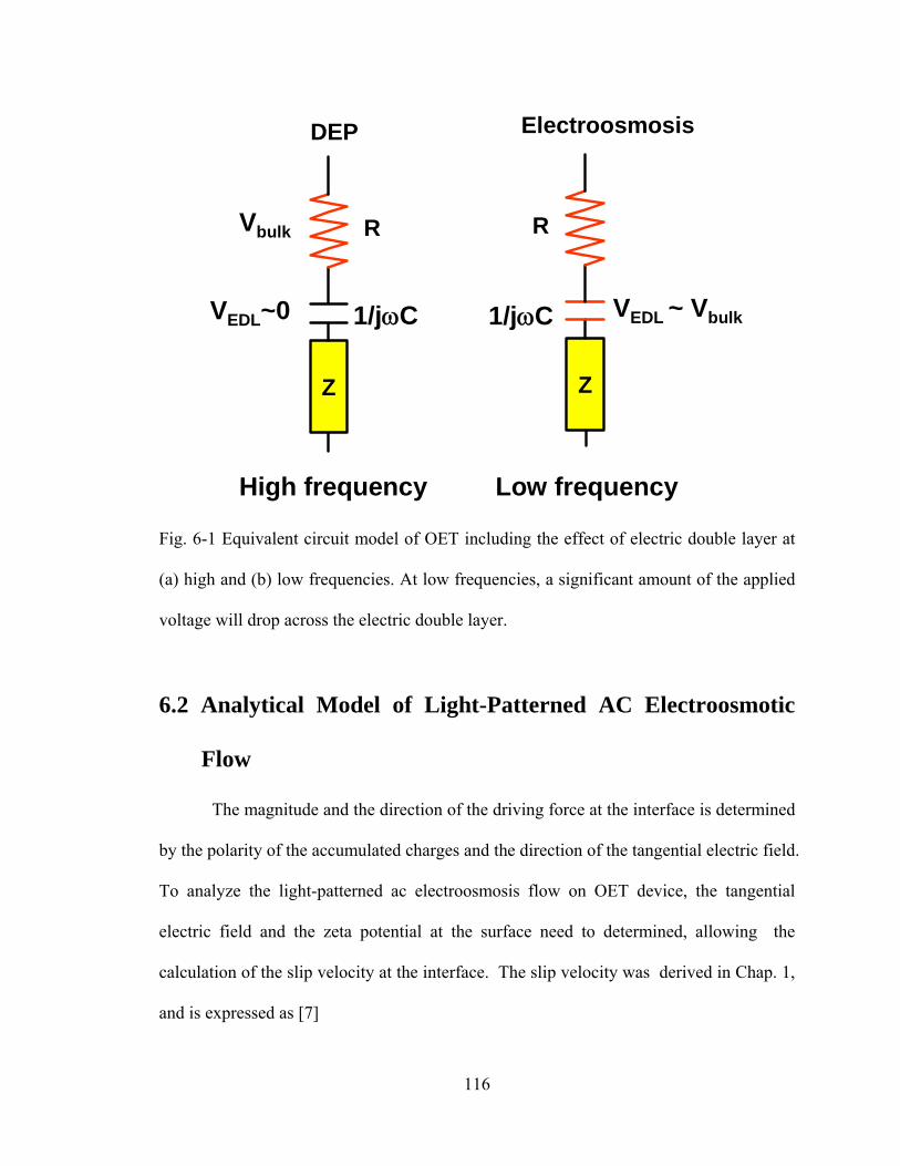
116
Z
1/jωC
R
Z
1/jωC
R
DEP Electroosmosis
High frequency Low frequency
VEDL~0 VEDL ~ Vbulk
Vbulk
Fig. 6-1 Equivalent circuit model of OET including the effect of electric double layer at
(a) high and (b) low frequencies. At low frequencies, a significant amount of the applied
voltage will drop across the electric double layer.
6.2 Analytical Model of Light-Patterned AC Electroosmotic
Flow
The magnitude and the direction of the driving force at the interface is determined
by the polarity of the accumulated charges and the direction of the tangential electric field.
To analyze the light-patterned ac electroosmosis flow on OET device, the tangential
electric field and the zeta potential at the surface need to determined, allowing the
calculation of the slip velocity at the interface. The slip velocity was derived in Chap. 1,
and is expressed as [7]
117
ηεE
v tslip
ζ−= (6.1)
where vslip is the slip velocity at the OET interface, ε is the permittivity of the liquid, Et is
the tangential component at the interface, ζ is the zeta potential as defined in Chap.1, and
η is the viscosity of the liquid.
Figure 6-2 illustrates the direction of the driving force and the induced
microfluidic flow pattern near the light-patterned virtual electrode. In the dark areas, both
the surface charge and the electric field strength at the interface are small, as the electric
impedance in the amorphous silicon layer dominates. As a result, the slip velocity at the
dark area is small. At the center of the virtual electrode, the voltage is switched to the
electric double layer and the bulk liquid layer. However, due to the symmetry of the
virtual electrode, there is no lateral electric field in the center, resulting in a slip velocity
of zero in the electrode center. At the edge of the virtual electrode, the fringing electric
field has lateral component which can drive the surface charges in the direction indicated
by Fig. 6-2. The slip velocity is strongest at the virtual electrode edge. The direction of
the velocity vector points to the center of the virtual electrode, creating a microfluidic
flow that is symmetrical about the virtual electrode. If a particle is near the virtual
electrode, it will be brought into the center of the virtual electrode by the light-patterned
microfluidic flow as a result of viscous force.
To analyze the slip velocity on the surface of the virtual electrode, we provide an
analytical model based on the equivalent circuit of OET. As shown in Fig. 6-3 (a), the
pattern of the electric field lines near the virtual electrode is highly non-uniform. The
electric field lines originating from the ITO surface converge to a small virtual electrode
on the photosensitive surface. Assuming the current flow in the lateral direction at the
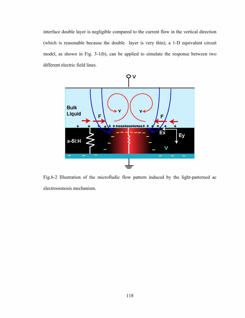
118
interface double layer is negligible compared to the current flow in the vertical direction
(which is reasonable because the double layer is very thin), a 1-D equivalent circuit
model, as shown in Fig. 3-1(b), can be applied to simulate the response between two
different electric field lines.
Fig.6-2 Illustration of the microfludic flow pattern induced by the light-patterned ac
electroosmosis mechanism.
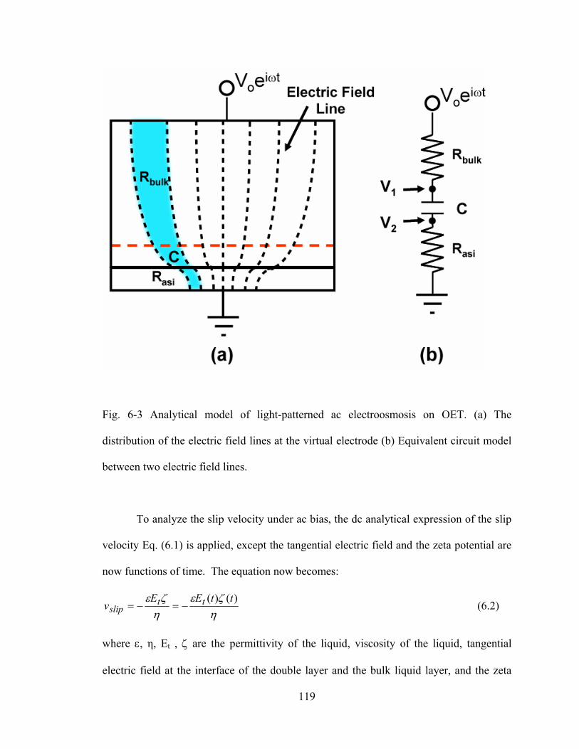
119
Fig. 6-3 Analytical model of light-patterned ac electroosmosis on OET. (a) The
distribution of the electric field lines at the virtual electrode (b) Equivalent circuit model
between two electric field lines.
To analyze the slip velocity under ac bias, the dc analytical expression of the slip
velocity Eq. (6.1) is applied, except the tangential electric field and the zeta potential are
now functions of time. The equation now becomes:
ηζε
ηζε )()( ttEE
v ttslip −=−= (6.2)
where ε, η, Et , ζ are the permittivity of the liquid, viscosity of the liquid, tangential
electric field at the interface of the double layer and the bulk liquid layer, and the zeta
120
potential, respectively. The applied signal is assumed to be sinusoidal, and is represented
by:
]Re[)(
]Re[)()( θω
ω
ζζ +=
=ti
o
titot
et
eEtE (6.3)
where θ is the phase difference between Et and ξ.
Substitute (6.3) into (6.2):
][41
]2
[]2
[
]Re[]Re[
)(
)2()2(
)()(
)(
θθθωθω
θωθωωω
θωω
ζηε
ζηε
ζηε
iititioto
titititioto
tio
tito
slip
eeeeE
eeeeE
eeE
tv
−+−+
+−+−
+
+++×−=
+×
+−=
×−=
)]cos()2[cos(21 θθωtE
ηε
oto ++×−= ζ (6.4)
The result of (6.4) shows that the slip velocity consists of an ac term and a dc term;
however, the net effect of the ac term is not observable in the kHz frequency range. The
values of Eto, ξo, and θ can be calculated from the equivalent circuit model.
The zeta voltage is approximated by the voltage drop across the interface double
layer capacitance and can be calculated as
]1
1
[
)(
21
CiR
CieVVV
t
tio
ω
ω
ζ
ω
+=−=
121
)(1 1φω += ti
o eZV (6.5)
where
22
221 ]
)(1[]
)(11[
RCRC
RCZ
RRR asibulk
ωω
ω ++
+=
+=
)(tan 11 RCωφ −= (6.6)
The electric field strength is not uniform along the electric field line – it is strongest at the
photoconductive surface, and monolithically decays towards the ITO surface. Et(t) can be
approximated as gVbulk/L, where Vbulk is the voltage drop across the bulk liquid layer, L is
the spacing between the photoconductive surface and the ITO glass, and g is the
geometry factor of the liquid resistance along one specific electric field line. It considers
the ratio of the length along the electric field line to the gap spacing L, the ratio of the
converging areas from the ITO surface to the double layer boundary, and the ratio of the
tangential component of the electric field at the double layer boundary. From the
equivalent circuit model,
]1
[
~)(
CiR
Re
LVg
LVgtE
bulktio
bulkt
ω
ω
+=
)(2 2φω += tio eZ
LVg (6.7)
where
122
)1(tan
])(1
[])(1
[
12
22
22
222
RC
RC
CR
RC
RRCZ bulkbulk
ωφ
ω
ω
ω
ω
−=
++
+=
(6.8)
Substituting (6.5) and (6.7) into (6.2) results in
)]cos()2[cos(2
~ 212
θθωη
ε++− t
LZZVg
v oslip (6.9)
where θ = φ1-φ2 is the phase difference between the tangential electric field and zeta
potential. If the ac term is neglected, a constant slip velocity is obtained, described by
)cos(2
~ 212
θη
εLZZVg
v oslip − (6.10)
In the low ac frequency range, where ωRC<<1, φ1~0, φ2~π/2, and cos(θ)=0, the slip
velocity approaches 0. In the high ac frequency range, where ωRC>>1, φ1~ π/2, φ2~0,
and cos(θ)=0, the slip velocity also approaches 0. The maximum slip velocity occurs at
an optimal frequency where ω=1/RC, φ1=φ2, and cos(θ)=1.
In the dark areas, R is dominated by the dark resistance of the amorphous silicon
layer, resulting in ωRC >> 1 and a very small slip velocity. At the center of the virtual
electrode, the slip velocity equals to zero since there is no tangential electric field.
Therefore, the driving force of the light-patterned ac electroosmotic flow is localized at
the edges of the virtual electrode. This property gives rise to the possibility of generating
a high-resolution microfluidic flow pattern for processing micro- and nano-scale particles.
123
6.3 Numerical Simulation of Light-patterned AC
Electroosmotic Flow
The simulation of the light-patterned ac electroosmostic flow is divided into two
parts. The first part is the calculation of the voltage drop across the double layer, the zeta
potential, and the tangential electric field at the interface of the double layer and the bulk
liquid. The second part is the calculation of the fluidic flow using the incompressible-
flow Navier-Stokes equation using the boundary slip velocity calculated in the first part
of the simulation.
The dc electrostatic model of the FEMLAB 3.0 software is used to simulate the
electric field distribution and the voltage drop across the double layer. The double layer
electrical impedance is converted to a resistance, REDL=1/ωC, where ω is the radian
frequency of the applied ac frequency and C is the double layer capacitance of the
solution. Figure 6-4 shows the simulated electric field distribution and the electrical
potential profile using the following parameters: thickness of the amorphous silicon layer
= 1 µm, dark conductivity of the amorphous silicon layer = 10-8 S/m, double layer
thickness = 10 nm, double layer dielectric constant = 78, liquid conductivity = 0.01 S/m,
ac frequency = 8 kHz, gap between the top and the bottom electrode = 100 µm, gaussian
beam spot size = 30 µm, peak conductivity of the amorphous silicon = 0.2 mS/m. The
tangential electric field strength at the interface of double layer and the bulk liquid is
extracted from Fig. 6-4(a), and is plotted in Fig. 6-5. The zeta potential, which is
extracted from the voltage drop across the double layer in Fig. 6-4(b), is shown in Fig. 6-
6. Multiplying the electric field strength in Fig. 6-5 with the zeta potential in Fig. 6-6
results in the slip velocity at different radial positions (Fig. 6-7).
124
0
0.5
1
1.5
2x10⁴
-2x10⁴
-0.5
-1
-1.5
R=100 µm
Electric FieldTangential Direction
(a) V/m
0
0.4
0.8
1.2
1.6
2 V
0.2
0.6
1.0
1.4
1.8
0.2
0.6
0.4
Bulk Liquid
Photoconductor
EDL
R=100 µm
Potential Profile
0
0.4
0.8
1.2
1.6
2 V
0.2
0.6
1.0
1.4
1.8
0.2
0.6
0.4
0.2
0.6
0.4
0.2
0.6
0.4
Bulk Liquid
Photoconductor
EDL
R=100 µm
Potential Profile(b)
Fig.6-4 (a) Tangential electric field in the bulk liquid layer. (b) The potential profile in
the bulk liquid layer. The potential drop across the electric double layer (EDL) is
extracted to calculate the zeta potential at the interface.
125
Fig.6-5 Radial distribution of the tangential electric field strength at the interface of the
double layer and the bulk liquid.
Fig.6-6 Radial distribution of the zeta potential at the interface between the
photoconductive surface and the solution. This potential is approximated by the voltage
drop across the double layer.
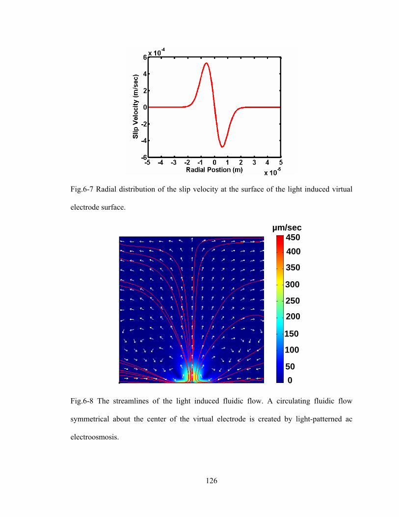
126
Fig.6-7 Radial distribution of the slip velocity at the surface of the light induced virtual
electrode surface.
0
300
350
400450
µm/sec
250
200
150
100
50
Fig.6-8 The streamlines of the light induced fluidic flow. A circulating fluidic flow
symmetrical about the center of the virtual electrode is created by light-patterned ac
electroosmosis.
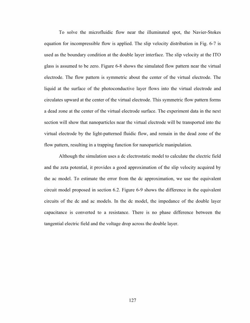
127
To solve the microfluidic flow near the illuminated spot, the Navier-Stokes
equation for incompressible flow is applied. The slip velocity distribution in Fig. 6-7 is
used as the boundary condition at the double layer interface. The slip velocity at the ITO
glass is assumed to be zero. Figure 6-8 shows the simulated flow pattern near the virtual
electrode. The flow pattern is symmetric about the center of the virtual electrode. The
liquid at the surface of the photoconductive layer flows into the virtual electrode and
circulates upward at the center of the virtual electrode. This symmetric flow pattern forms
a dead zone at the center of the virtual electrode surface. The experiment data in the next
section will show that nanoparticles near the virtual electrode will be transported into the
virtual electrode by the light-patterned fluidic flow, and remain in the dead zone of the
flow pattern, resulting in a trapping function for nanoparticle manipulation.
Although the simulation uses a dc electrostatic model to calculate the electric field
and the zeta potential, it provides a good approximation of the slip velocity acquired by
the ac model. To estimate the error from the dc approximation, we use the equivalent
circuit model proposed in section 6.2. Figure 6-9 shows the difference in the equivalent
circuits of the dc and ac models. In the dc model, the impedance of the double layer
capacitance is converted to a resistance. There is no phase difference between the
tangential electric field and the voltage drop across the double layer.
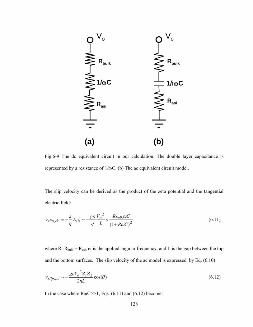
128
Rbulk
Rasi
Vo
1/iωC
(b)
Rbulk
Rasi
Vo
1/ωC
(a)
Fig.6-9 The dc equivalent circuit in our calculation. The double layer capacitance is
represented by a resistance of 1/ωC. (b) The ac equivalent circuit model.
The slip velocity can be derived as the product of the zeta potential and the tangential
electric field:
2
2
,)1(
~CR
CRLVgEv bulko
tdcslipω
ωηεξ
ηε
+×−−= (6.11)
where R=Rbulk + Rasi, ω is the applied angular frequency, and L is the gap between the top
and the bottom surfaces. The slip velocity of the ac model is expressed by Eq. (6.10):
)cos(2
~ 212
, θη
εLZZVg
v oacslip − (6.12)
In the case where RωC>>1, Eqs. (6.11) and (6.12) become:
129
CR
RLVgv bulko
dcslipωη
ε2
2
, ~ ×− (6.13)
2)cos(~ 2
2
,θ
ωηε
××−CR
RLVgv bulko
acslip (6.14)
The magnitude of the slip velocities simulated by both models is small, since RωC>>1.
However, the result of the ac model is smaller than that of the dc model, due to the extra
phase term. When RωC>>1, the cos(θ) term approaches zero. This occurs when R is
large in the dark area or when ω is large in the high ac frequency regime.
In the case where RωC<<1, Eqs. (6.11) and (6.12) become:
ωCRLV
ηgε~v bulk
oslip,dc ×−
2 (6.14)
2)cos(~
2
,θω
ηε
××− CRLVgv bulko
acslip (6.15)
The magnitude of the slip velocities simulated by both models is again small. Again, the
slip velocity magnitude is smaller in ac model, due to the extra phase term. The cos(θ)
term also approaches zero when RωC <<1. This occurs when the ac frequency is low.
In the case where RωC ~ 1, Eqs. (6.11) and (6.12) become:
LVgv o
dcslip
2
, 41~ηε
− (6.15)
)cos(41~
2
, θηεLVgv o
acslip − (6.16)
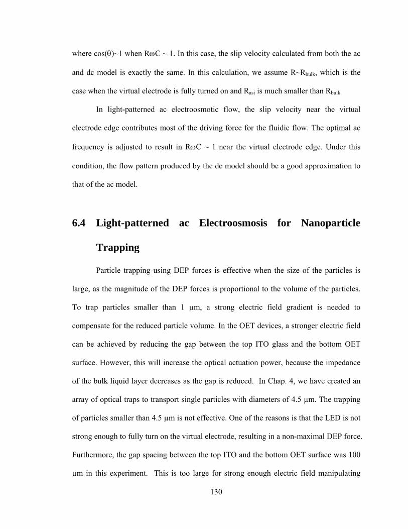
130
where cos(θ)~1 when RωC ~ 1. In this case, the slip velocity calculated from both the ac
and dc model is exactly the same. In this calculation, we assume R~Rbulk, which is the
case when the virtual electrode is fully turned on and Rasi is much smaller than Rbulk.
In light-patterned ac electroosmotic flow, the slip velocity near the virtual
electrode edge contributes most of the driving force for the fluidic flow. The optimal ac
frequency is adjusted to result in RωC ~ 1 near the virtual electrode edge. Under this
condition, the flow pattern produced by the dc model should be a good approximation to
that of the ac model.
6.4 Light-patterned ac Electroosmosis for Nanoparticle
Trapping
Particle trapping using DEP forces is effective when the size of the particles is
large, as the magnitude of the DEP forces is proportional to the volume of the particles.
To trap particles smaller than 1 µm, a strong electric field gradient is needed to
compensate for the reduced particle volume. In the OET devices, a stronger electric field
can be achieved by reducing the gap between the top ITO glass and the bottom OET
surface. However, this will increase the optical actuation power, because the impedance
of the bulk liquid layer decreases as the gap is reduced. In Chap. 4, we have created an
array of optical traps to transport single particles with diameters of 4.5 µm. The trapping
of particles smaller than 4.5 µm is not effective. One of the reasons is that the LED is not
strong enough to fully turn on the virtual electrode, resulting in a non-maximal DEP force.
Furthermore, the gap spacing between the top ITO and the bottom OET surface was 100
µm in this experiment. This is too large for strong enough electric field manipulating
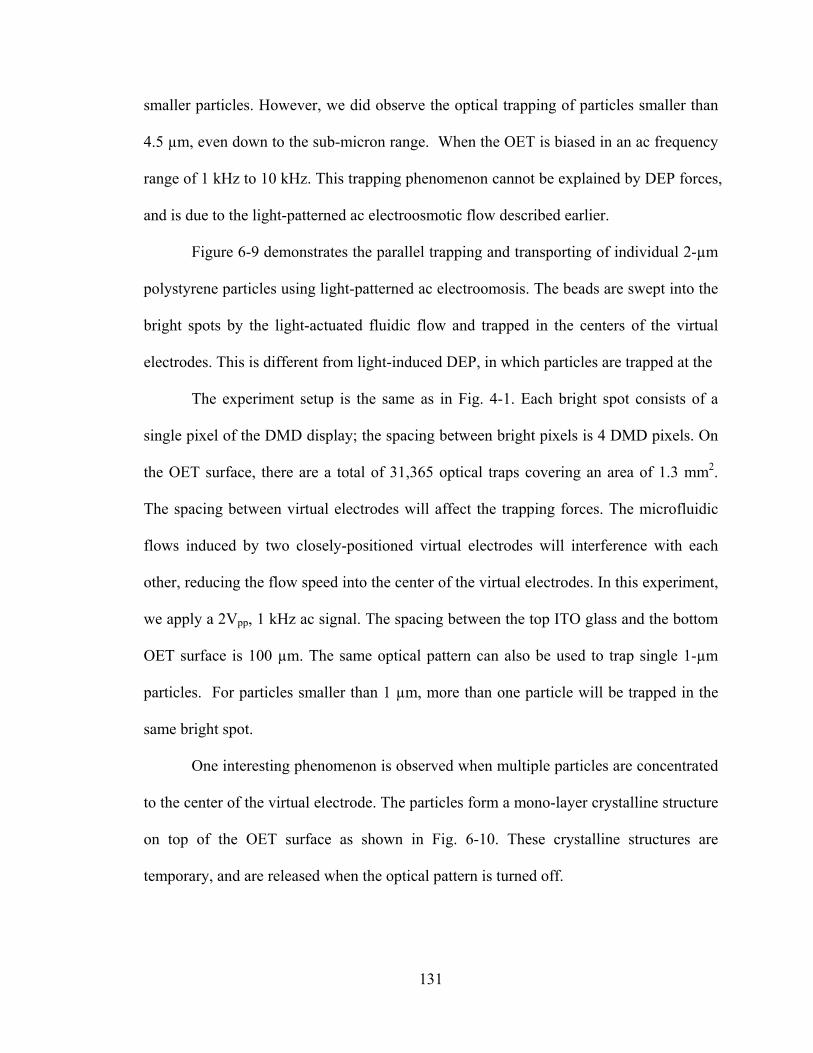
131
smaller particles. However, we did observe the optical trapping of particles smaller than
4.5 µm, even down to the sub-micron range. When the OET is biased in an ac frequency
range of 1 kHz to 10 kHz. This trapping phenomenon cannot be explained by DEP forces,
and is due to the light-patterned ac electroosmotic flow described earlier.
Figure 6-9 demonstrates the parallel trapping and transporting of individual 2-µm
polystyrene particles using light-patterned ac electroomosis. The beads are swept into the
bright spots by the light-actuated fluidic flow and trapped in the centers of the virtual
electrodes. This is different from light-induced DEP, in which particles are trapped at the
The experiment setup is the same as in Fig. 4-1. Each bright spot consists of a
single pixel of the DMD display; the spacing between bright pixels is 4 DMD pixels. On
the OET surface, there are a total of 31,365 optical traps covering an area of 1.3 mm2.
The spacing between virtual electrodes will affect the trapping forces. The microfluidic
flows induced by two closely-positioned virtual electrodes will interference with each
other, reducing the flow speed into the center of the virtual electrodes. In this experiment,
we apply a 2Vpp, 1 kHz ac signal. The spacing between the top ITO glass and the bottom
OET surface is 100 µm. The same optical pattern can also be used to trap single 1-µm
particles. For particles smaller than 1 µm, more than one particle will be trapped in the
same bright spot.
One interesting phenomenon is observed when multiple particles are concentrated
to the center of the virtual electrode. The particles form a mono-layer crystalline structure
on top of the OET surface as shown in Fig. 6-10. These crystalline structures are
temporary, and are released when the optical pattern is turned off.
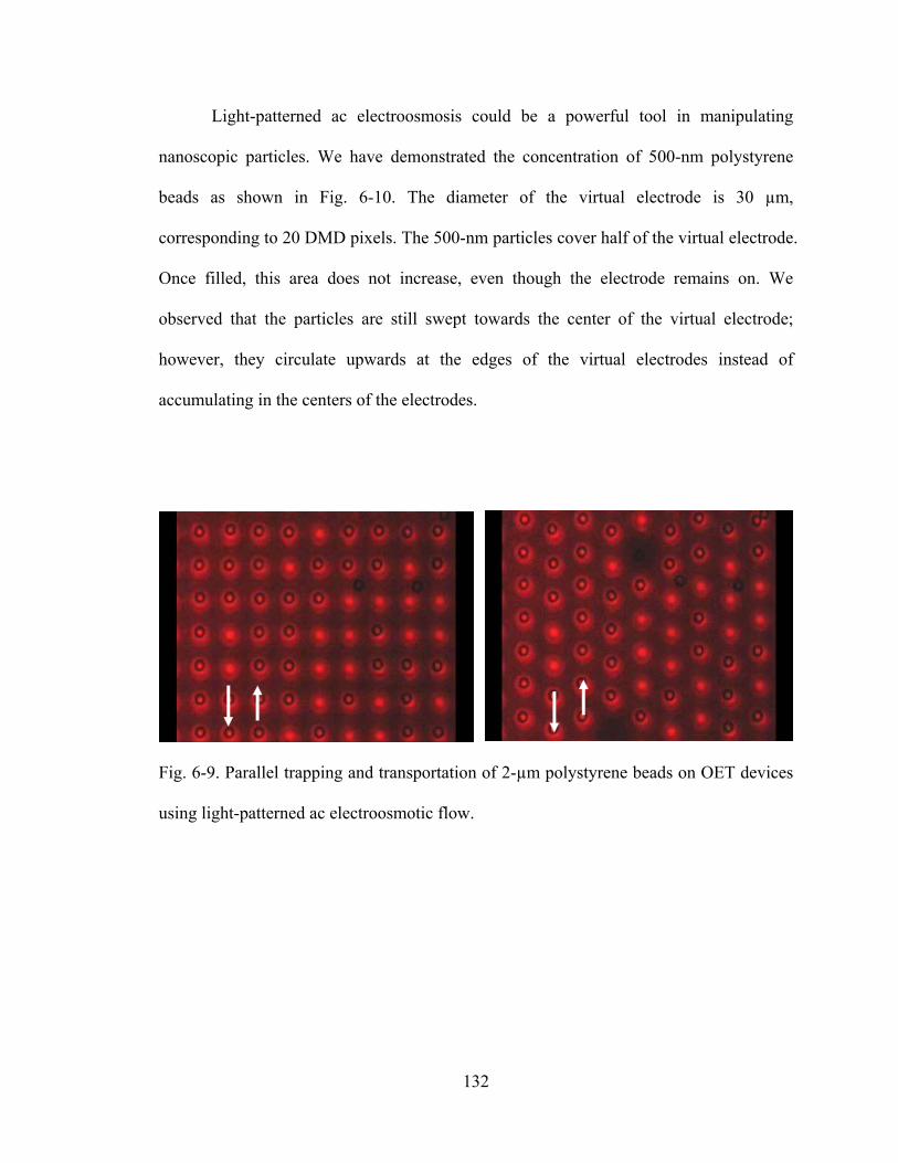
132
Light-patterned ac electroosmosis could be a powerful tool in manipulating
nanoscopic particles. We have demonstrated the concentration of 500-nm polystyrene
beads as shown in Fig. 6-10. The diameter of the virtual electrode is 30 µm,
corresponding to 20 DMD pixels. The 500-nm particles cover half of the virtual electrode.
Once filled, this area does not increase, even though the electrode remains on. We
observed that the particles are still swept towards the center of the virtual electrode;
however, they circulate upwards at the edges of the virtual electrodes instead of
accumulating in the centers of the electrodes.
Fig. 6-9. Parallel trapping and transportation of 2-µm polystyrene beads on OET devices
using light-patterned ac electroosmotic flow.
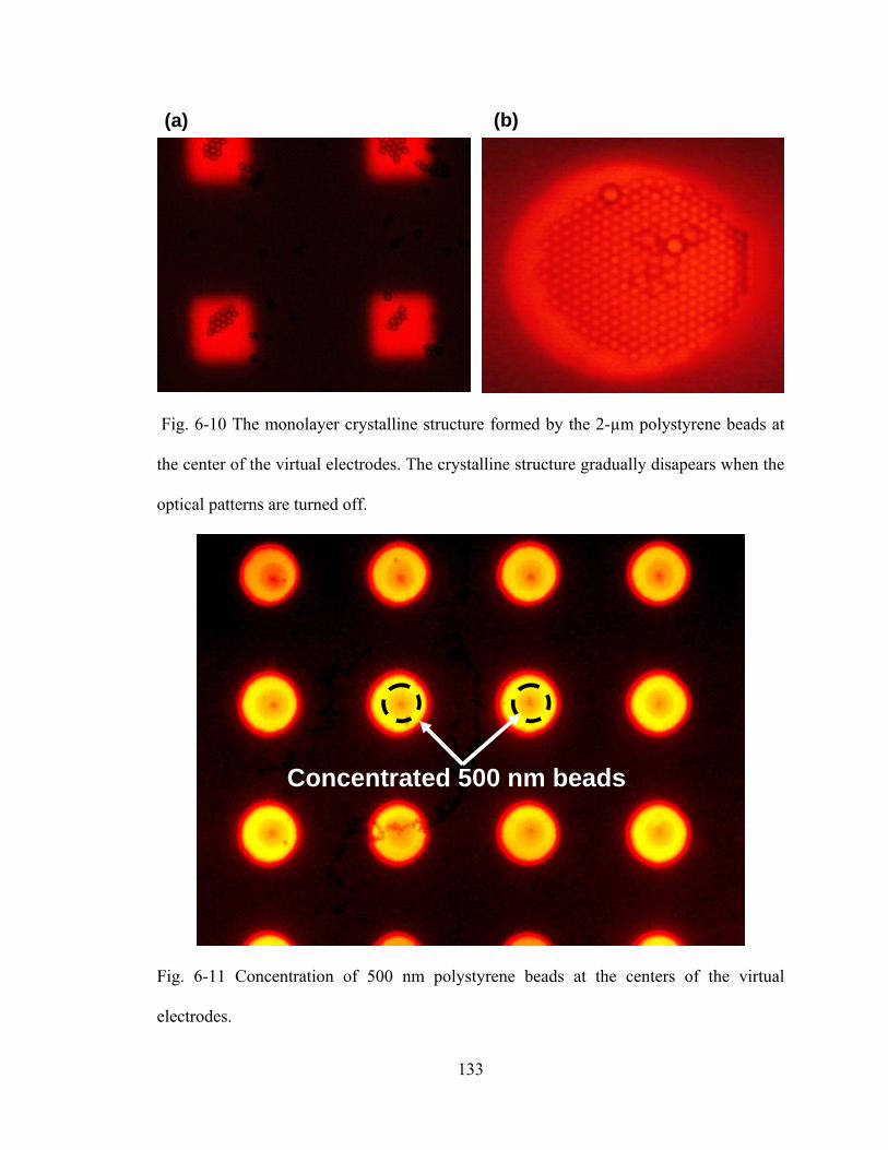
133
(b)(a)
Fig. 6-10 The monolayer crystalline structure formed by the 2-µm polystyrene beads at
the center of the virtual electrodes. The crystalline structure gradually disapears when the
optical patterns are turned off.
Concentrated 500 nm beads
Fig. 6-11 Concentration of 500 nm polystyrene beads at the centers of the virtual
electrodes.
134
To quantify the velocity of the light-patterned ac electroosmotic flow, the particle
speed near the edge of the virtual electrode is measured at different ac frequencies. Due
to limitations of our current CCD camera, the particle speed is measured at ~17 µm radial
distance from the center of a circular virtual electrode with a radius of 15 µm. The
particle velocity inside the edge of the virtual electrode is greater than 100 µm/s, which is
too fast to be captured by our current CCD camera. Figure 6-12 shows the measured
result using 1-µm beads under a 4Vpp ac bias. The flow speed is frequency dependent as
predicted by the analytical model in Sec. 6-2. The optimal frequency shown here is
around 8 kHz. The data at frequencies above 12 kHz is not collected, since the DEP
force become more effective at these higher frequencies, and starts to compete with the
decreasing forces from light-patterned fluidic flow.
Fig. 6-12. The frequency response of the light-patterned ac electroosmotic flow near the
edge of the virtual electrode.
135
6.5 Reference
[1] A. Ramos, H. Morgan, N. G. Green, and A. Castellanos, "Ac electrokinetics: a
review of forces in microelectrode structures," Journal Of Physics D-Applied
Physics, vol. 31, pp. 2338-2353, 1998.
[2] T. Muller, A. Gerardino, T. Schnelle, S. G. Shirley, F. Bordoni, G. DeGasperis, R.
Leoni, and G. Fuhr, "Trapping of micrometre and sub-micrometre particles by
high-frequency electric fields and hydrodynamic forces," Journal Of Physics D-
Applied Physics, vol. 29, pp. 340-349, 1996.
[3] N. G. Green, A. Ramos, A. Gonzalez, H. Morgan, and A. Castellanos, "Fluid flow
induced by nonuniform ac electric fields in electrolytes on microelectrodes. III.
Observation of streamlines and numerical simulation," Physical Review E, vol. 66,
2002.
[4] A. Gonzalez, A. Ramos, N. G. Green, A. Castellanos, and H. Morgan, "Fluid flow
induced by nonuniform ac electric fields in electrolytes on microelectrodes. II. A
linear double-layer analysis," Physical Review E, vol. 61, pp. 4019-4028, 2000.
[5] N. G. Green, A. Ramos, A. Gonzalez, H. Morgan, and A. Castellanos, "Fluid flow
induced by nonuniform ac electric fields in electrolytes on microelectrodes. I.
Experimental measurements," Physical Review E, vol. 61, pp. 4011-4018, 2000.
[6] A. Ramos, A. Gonzalez, A. Castellanos, H. Morgan, and N. G. Green, "Fluid flow
driven by a.c. electric fields in microelectrodes," in Electrostatics 1999, vol. 163,
Institute Of Physics Conference Series, 1999, pp. 137-140.
[7] R. J. Hunter, Zeta Potential in Colloid Science. New York: Academic Press Inc.,
1981.
136
CHAPTER 7
Conclusion
We have proposed a novel optoelectronic tweezers (OET) that enables massively
parallel optical manipulation of single cells, micro-particles, and nano-particles. It is
realized by using light to pattern virtual electrode on a photoconductive surface and
induce the dielectrophoretic force. Since the optical energy is not directly converted to
the mechanical force, as in optical tweezers, OET can operate at extremely low optical
power. We have demonstrated optical manipulation of microscopic particles with light
intensity as low as 1 W/cm2, which is five orders of magnitude less than that in optical
tweezers techniques. This opens up the possibility of optical manipulation using cheap
incoherent light source such as a lamp or a LED.
Integrating a DMD spatial light modulator with 1024×768 pixels array, we can
create 15,000 particle traps on a 1.3×1 mm2 area using a single LED light bulb. The
resolution of the optically patterned virtual electrode is limited by the optical diffraction
limit of the optics used for image projection and can achieve sum-micron resolution.
Since the optical pattern is real-time reconfigured on the spatial light modulator, dynamic
electric field landscape of any arbitrary shape can be created to perform multi-step and
integrated manipulation functions. Further integration of OET with image feedback
system, a fully automatic optical manipulation system can be achieved for high
throughput manipulation.
137
The concept of light-addressed virtual electrodes can be extended to other
electrokinetic mechanisms. We have demonstrated an light induced ac electroosmosis
mechanism to pattern localized microfluidic flow near each virtual electrode. Nanoscopic
particles, which is difficult to manipulate using dielectrophoretic forces, can be
manipulated in the low flow region. This mechanism allows us to generate 31,000 single
particle traps to transport 1-µm beads in parallel. We have also demonstrated the
concentration of 500-nm particles. This technology has the potential to manipulate many
interesting nanoscopic particles such as quantum dots, carbon nanotubes nanowires, and
biomolecules such as DNAs and proteins.