Prof. Glenn Boreman Physics Optical Science Center
53
Prof. Glenn Boreman Prof. Glenn Boreman Chair, Department of Physics & Optical Science Chair, Department of Physics & Optical Science Director, Optoelectronics Center Director, Optoelectronics Center [email protected] [email protected] 704 687 8173 704 687 8173
Transcript of Prof. Glenn Boreman Physics Optical Science Center

Prof. Glenn BoremanProf. Glenn BoremanChair, Department of Physics & Optical ScienceChair, Department of Physics & Optical ScienceDirector, Optoelectronics CenterDirector, Optoelectronics [email protected]@uncc.edu704 687 8173704 687 8173

Deposition/Deposition/EtchingEtching
Contact: Robert Hudgins
Process achieves high microns/minute rate anisotropic etching using the Bosch processVertical etch depths of >0.5 mmAspect ratios approaching 20:1Gases: C4F8, O2, SF6, Ar, He
200 nm holes
200 nm posts

Inductively Coupled Plasma system uses chlorine based chemistry to etch compound semiconductor materials such as GaAs, GaN, InP, GaP, SiC, and AL203Uniform anisotropic etching of thin film materialsPower RF generatorsGases: Ar, O2, SF6, SiCl4, He, N2, Cl2, BCl3
Contact: Robert Hudgins
Deposition/Deposition/EtchingEtching

Contact: Robert Hudgins
Employs fluorine plasma chemistries to etch dielectrics, including SiO2 and Si3N4Available Gases: SF6, O2, C4F8, H2, CHF3, HeRF Power:
Coil ‐ 3 Kw at 13.56 MHzPlaten – 600 w at 13.56 MHz
Deposition/Deposition/EtchingEtching

High quality SiO2, Si3N4Uses 100 mm substratesLow frequency and high frequency generationGases: C4F8O2, NH3, N2, N2O, SiH4
Contact: Robert Hudgins
Deposition/Deposition/EtchingEtching
© SSI Surface Science Integration
Contact: Oleg Smolski
Process up to 150mm‐dia substrates at a temperature range from RT‐1000⁰ CTemperature Ramp‐Up 25⁰C/secPID process controller ensures accurate temperature stability and uniformityDesigned for silicon implant annealing and monitoring, compound semiconductor implant activation and ohmic contact alloyingGases: N2, Ar, 02
Deposition/Deposition/EtchingEtching

Contact: Robert Hudgins
ATC 1800‐F sputter deposition systemWafers up to 150 mm in diameterSingle layer, sequential, or co‐sputtered processesPlaten can be rotated for enhanced thickness uniformityGas: Ar
© AJA International, Inc.
Deposition/Deposition/EtchingEtching

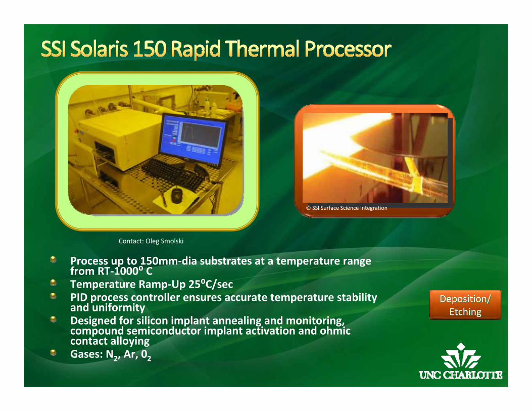
Contact: Lou Deguzman
Electron‐beam and thermal evaporation system10‐8 Torr VacuumCapacity of processing three 100 mm wafers or a single 150, 200, or 300 mm waferRuns in manual or automatic modeUp to 4 deposition materialsBeneficial for lift‐off metallization
Blue wavelength LEDs, Stokes Group 2‐layer metal thin film, etched
VA‐CNTs on Si chip
Cantilever with VA‐CNTs grown on Fe film
M. Forney, Poler Group
Deposition/Deposition/EtchingEtching

Step and Flash Imprint Lithography TechnologyStep and Flash Imprint Lithography TechnologyResolution : subResolution : sub‐‐50 nm 50 nm Alignment : < 500 nmAlignment : < 500 nmWafer handling: up to 8Wafer handling: up to 8‐‐inch diameter wafersinch diameter wafers66””, 4, 4”” and 3and 3”” diameter wafer chucks availablediameter wafer chucks availableField size : 25 mm maximumField size : 25 mm maximumMiniMini‐‐environment:environment: Class 3Class 3
Contact: Lou Deguzman
80nm posts 150nm holes
70nm lines cgh
LithographyLithography

Ultra high resolution patterningMinimum feature size < 20 nmOverlay capability: < 60 nmStitching capability: < 60 nmMagnification: 20x ‐ 1,000,000xUltra high resolution imaging
100nm posts
Contact: Lou Deguzman
Suleski Group
180 nm lines on 360 nm pitch
IR polarization filter on silicon
LithographyLithography
Contact: Lou Deguzman A. Cannistra, Suleski Group
Reflowed Lenses High aspect ratio SU‐8 structures
Hybrid lithography
For 100mm and 150mm wafers, and piece partsVacuum, pressure, and proximity mask exposureSub‐um lithography in vacuum contact mode Split Field Alignment MicroscopeOverlay accuracy:
Frontside alignment: ~ 0.5 umBackside alignment: ~ 1 to 2 um
LithographyLithography
Contact: Lou Deguzman
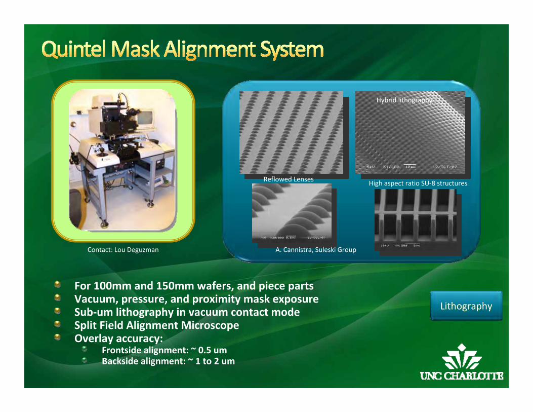
5X reduction projection lithography toolG‐Line 436 nm wavelength4” 1mm thick wafers, silicone and fused silicaSingle wafer chuck
LithographyLithography
Contact: Robert Hudgins

Ball‐Wedge bonding wire capabilityOlympus microscope and spotlight targetingDeep access capabilityFlat substrate holder with built‐in temperature controllerMotorized Y axis and programmable auto‐stepbackfunction for precise wire length and loop formationAuto‐2nd bond mode for complete single wire programmed sequenceDigital readout of all parameters etc
Contact: Oleg Smolski
PackagingPackaging
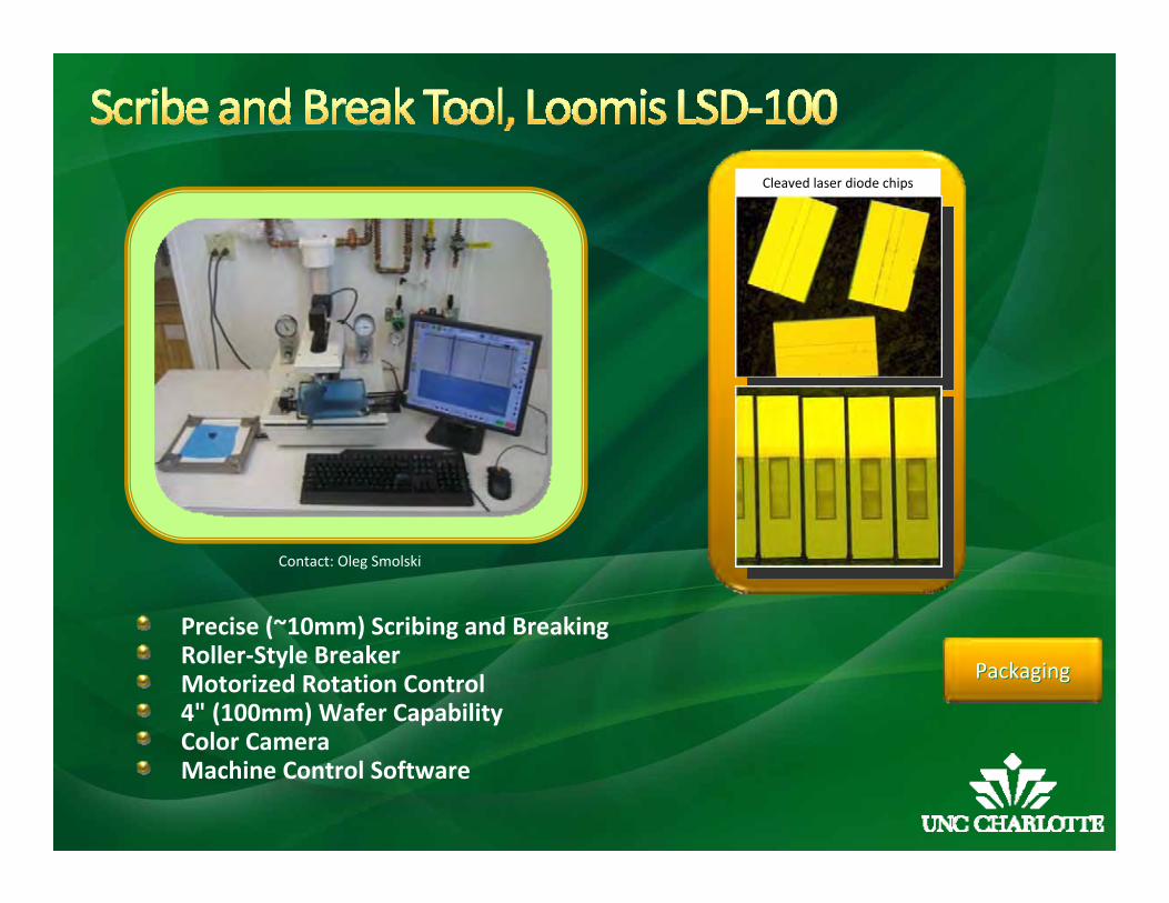
Contact: Oleg Smolski
Precise (~10mm) Scribing and BreakingRoller‐Style BreakerMotorized Rotation Control4" (100mm) Wafer CapabilityColor CameraMachine Control Software
Cleaved laser diode chips
PackagingPackaging
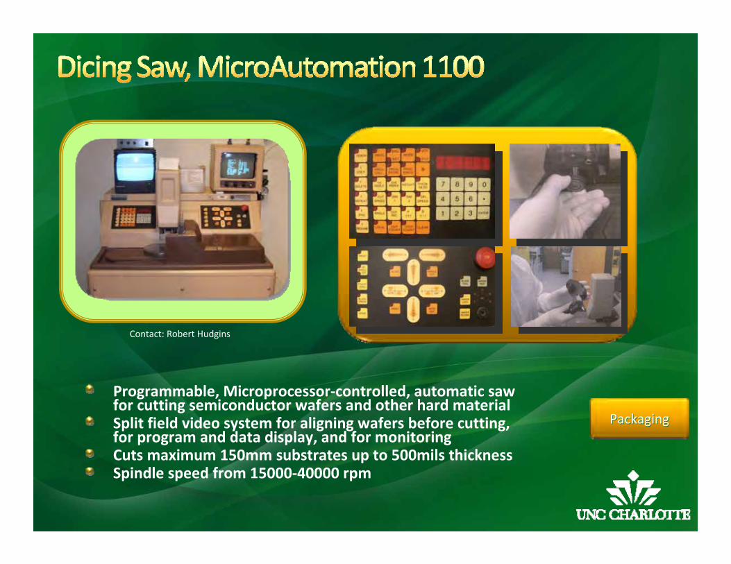
Programmable, Microprocessor‐controlled, automatic saw for cutting semiconductor wafers and other hard materialSplit field video system for aligning wafers before cutting, for program and data display, and for monitoringCuts maximum 150mm substrates up to 500mils thicknessSpindle speed from 15000‐40000 rpm
Contact: Robert Hudgins
PackagingPackaging

Flip‐Chip bonding capabilitySubstrates up to 50x50 mm2
Placement accuracy is ± 1.0 µmPC‐controlled heating plate (up to 400oC)Bonding force range: 0.1 N ‐ 500 N
Contact: Oleg Smolski
(2x2) 2D vertical assembly of the surface‐emitters bars
1D vertical stack of the surface‐emitting devices
Device in operation
Device in operation
PackagingPackaging

Gold ribbon (≤250mm‐wide) wiring for high‐speed and high‐current applicationNikon microscope and spotlight targetingDeep access capabilityFlat substrate holder with built‐in temperature controllerMotorized Y axis and programmable auto‐stepback function for precise wire length and loop formationDigital readout of all parameters
Contact: Oleg Smolski
Gold ribbon wedge bonding
PackagingPackaging

Advanced materials science and nanotechnology diffractionMetrologic characterization in semiconductor process developmentIt can handle a wide range of applications, and is especially suitable for thin film analysis applications such as:
Rocking curve analysis and reciprocal space mappingReflectometry and thin film phase analysisResidual stress and texture analysis
Contact: Lou Deguzman
Imaging/Imaging/CharacterizationCharacterization
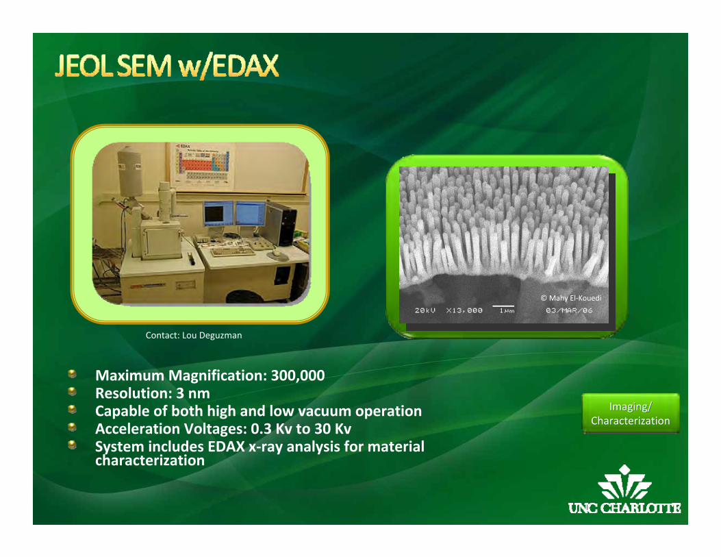
Maximum Magnification: 300,000Resolution: 3 nmCapable of both high and low vacuum operationAcceleration Voltages: 0.3 Kv to 30 KvSystem includes EDAX x‐ray analysis for material characterization
©Mahy El‐Kouedi
Contact: Lou Deguzman
Imaging/Imaging/CharacterizationCharacterization

Surface imaging technique for analyzing nanoscale and atomic structuresSub‐nm ResolutionMultiple scanning modes, including:
ContactTappingMagnetic
Contact: Robert Hudgins
Multi‐layer IRpolarization filter
Imaging/Imaging/CharacterizationCharacterization

Five Key Laser Technologies:Under short‐wavelength laser sourceConfocal Optical SystemXY ScanReal Color Image AcquisitionLinear Scale Z‐scanning
Seven Measurement Modes:Step MeasurementSurface Roughness MeasurementArea/Volume MeasurementParticle MeasurementFilm Thickness MeasurementUnder Geometric MeasurementAuto Edge Detection Measurement
Contact: Robert Hudgins
Imaging/Imaging/CharacterizationCharacterization

Spectral Range: 193 to 1700 nmWVASE32® data analysis softwareMeasures:
Thin film thicknessOptical constants (n and k)Spectral transmittance and reflection
Focusing optics for 200 um spot size
Contact: Lou Deguzman
Imaging/Imaging/CharacterizationCharacterization

Continuum Pulsed Q‐switched Nd YAG 8000 series LaserWarms up to full energy in less than 5 minutesExcellent beam quality and pointing stability
Panther OPO (Optical Parametric Oscillator)Linewidth of down to less than 1.5 cm‐1Signal energies to > 150 mJ per pulseComplete tunability with no degeneracy gap (205 – 2550 nm)
© Continuum Lasers
Contact: Scott Williams
LaserLaserFacilityFacility

Dr. Glenn Boreman, Center Director704‐687‐8173, [email protected]
Mark Clayton, Communications/Website704‐687‐8117, [email protected]
Dr. Lou Deguzman, Research Staff 704‐687‐8111, [email protected]
Dr. Robert Hudgins, Cleanroom Operations Manager704‐687‐8125, [email protected]
Dr. Oleg Smolski, Research Professor704‐687‐8288, [email protected]
Margaret Williams, Business Manager704‐687‐8106, [email protected]
Scott Williams, Research Operations Manager704‐687‐8126, [email protected]

UNCC’s Optoelectronics Center has capabilities complementary to CPM in the area of optical metrology.
These include precise measurement of dimensional metrology for films and optical elements, measurement of optical properties of materials, and scattered light instrumentation for surface-finish assessment.
All instruments listed are available in UNCCs user facility.
Contact Info:Dr. Glenn Boreman, Dept. Chair & Center [email protected], 704 687 8173
Dr. Angela Davies, Assoc. Prof. – Optical [email protected], 704 687 8135

4mm
Optic characterization (mm‐scale) 633 nm wavelength Form metrology of near flat and spherical optical‐quality
components (2mm – 10mm aperture)Radius of curvature (1mm –
30mm)Optical system alignment
Contact: Angela Davies
Micro-Interferometer

Contact: Angela Davies
633 nm wavelengthForm metrology of near flat and spherical optical‐quality
componentsRadius of curvature (1cm‐1m)Optical system alignment4”
–
0.6”
aperture (flat measurements)
Phase Shifting Interferometer

FusedSilicaWafer
front backFront Surface
Back Surface
dd
Contact: Angela Davies
t
~330nm PV
~20 m bowhomogeneity
100 ppmPV
NdYAG
Crystal34 ppm
PV
1550 nm wavelengthAbsolute thickness as low as 1mm4”‐1”
apertureHomogeneityWindow dimensional metrology
Wedge and flatness (thickness
variation)
Wavelength Scanning Interferometer

633 nm wavelengthSub‐mm Aperture Lenses
Form ErrorRadiusFocal LengthWave front Aberration
Contact: Angela Davies
Micro-optic Reflection and Transmission Interferometer
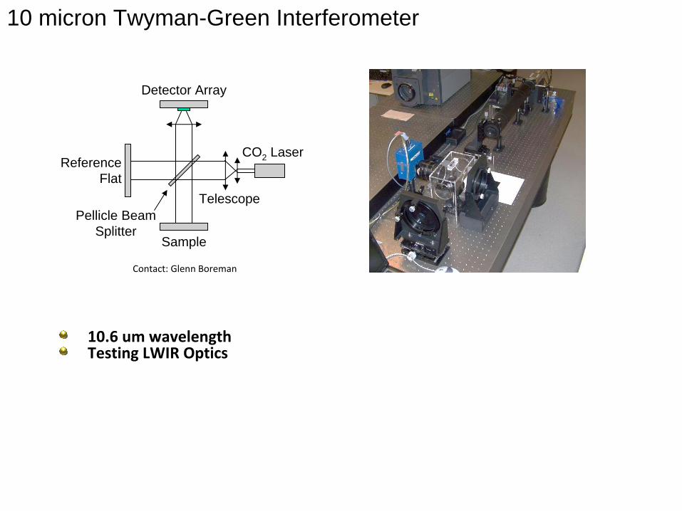
Reference Flat
Sample
Detector Array
Telescope
CO2 Laser
Pellicle Beam Splitter
10 micron Twyman-Green Interferometer
Contact: Glenn Boreman
10.6 um wavelengthTesting LWIR Optics
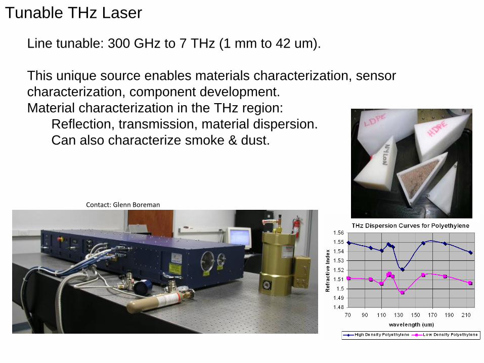
Line tunable: 300 GHz to 7 THz (1 mm to 42 um).
This unique source enables materials characterization, sensor characterization, component development.Material characterization in the THz region:
Reflection, transmission, material dispersion. Can also characterize smoke & dust.
Tunable THz Laser
Contact: Glenn Boreman

Measure refractive index, attenuation, conductivity from 400 nm (blue end of VIS) to 40 um in the far IR (continuous coverage)
Ellipsometers
Contact: Glenn Boreman
VIS/NIR Ellipsometer IR/FIR Ellipsometer

Measure reflection, transmission, absorption in SWIR, MWIR & LWIR100 um spatial resolution
FTIR Microscope
Contact: Glenn Boreman

Measure surface emissivity in MWIR & LWIRNear-plane imaging and far-field imaging available
IR Spectro-radiometer
Contact: Glenn Boreman

Measure surface roughness & subsurface damage using scattered lightVIS and LWIR laser, as well as spectrally resolved MWIR/LWIR
Scatterometers
Contact: Glenn Boreman

Measure vector electric field in 3D with 20 nm spatial resolution
E-field Mapper
Contact: Glenn Boreman

Contact Info:Dr. Glenn Boreman, Dept. Chair & Center Director [email protected], 704 687 8173
Scott Williams, Research Operations Manager Center for Optoelectronics and Optical Communications
[email protected], 704 687 8126
Optical Communication Infrastructure Facility

Contact: Scott Williams 704-687-8126 [email protected]
Fiber Optic Connector Assembly
Capabilities•Connector assembly of most major connectors and
manufacturers including.• FC, FC/Angle, SC, SC/Angle, ST, LC, MU,
MTRJ, FDDI, ESCON, DIN, Biconic, SMA•Assemblies done on most size fiber including large
core.• 250um coated• 900um coated• 1.6mm Jacketed• 2.0mm Jacketed• 3.0mm Jacketed
•Assembles on large count cables.• Loose Tube• Distribution• Breakout

Contact: Scott Williams 704-687-8126 [email protected]
Fiber Optic Connector Testing
Capabilities•Connector end face inspection at 400x for most
connector styles•Connector testing for most connector style.
• (IL) Insertion Loss• (RL) Return Loss
•End Face Geometry checked with Norland
Connect‐Check 6000• Apex Offset• Fiber Protrusion/Undercut• Radius of Curvature• Angle
•Full reporting Capabilities

Technical Data
Current Connector Types MT
Connector types that can
be added
FC, LC, LC/Angle, LX.5,
MT/Angle, MTRJ,
MTRJ/Angle, MU, SC,
SC/Angle, SMA, Ferrule
Only
Pressure TypePneumatic
Platen Size 5in.
Contact: Scott Williams 704-687-8126 [email protected]
Domaille EngineeringOptical Fiber Polishing MachineModel: HDC‐4000

Technical Data
Current Connector Types FC, FC/Angle
Connector types that can
be added
LC, LC/Angle, MU,
MU/Angle, ST, SC,
SC/Angle, E2000,
E2000/Angle, Ferrule
Only, Ferrule only/Angle
Pressure TypeSpring
Platen Size 4in.
Contact: Scott Williams 704-687-8126 [email protected]
Seiko InstrumentsOptical Fiber Polishing MachineModel: OFL‐12
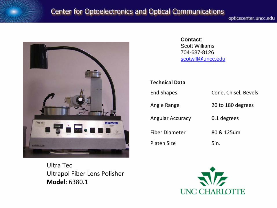
Technical Data
End Shapes Cone, Chisel, Bevels
Angle Range 20 to 180 degrees
Angular Accuracy 0.1 degrees
Fiber Diameter 80 & 125um
Platen Size 5in.
Contact: Scott Williams 704-687-8126 [email protected]
Ultra TecUltrapol Fiber Lens PolisherModel: 6380.1

Technical Data
Fibers
Single‐mode, multimode,
dispersion‐shifted,
Polarization maintaining,
erbium
Typical splice losses 0.02 dB SM fibers
Contact: Scott Williams 704-687-8126 [email protected]
Ericsson Fusion SplicerModel: FSU 975 PM‐A

Technical Data
FibersSingle‐mode, multimode,
dispersion‐shifted,
Polarization maintaining,
Typical splice losses0.07dB PM fibers0.03dB SM fibers0.02dB MM fibers
Typical Extinction ratio >30dB
Contact: Scott Williams 704-687-8126 [email protected]
Fujikura Fusion SplicerModel: FSM‐20PMII

Technical Data
Fibers
Single‐mode, Multimode,
Dispersion‐shifted, Non‐
zero dispersion shifted,
Cut‐off shifted, Erbium
doped
Typical splice losses0.02dB SM fibers0.01dB MM fibers0.04dB NZDS fibers
Typical return loss >60dB
Contact: Scott Williams 704-687-8126 [email protected]
Fujikura Fusion SplicerModel: FSM‐40S
Contact: Scott Williams 704-687-8126 [email protected]
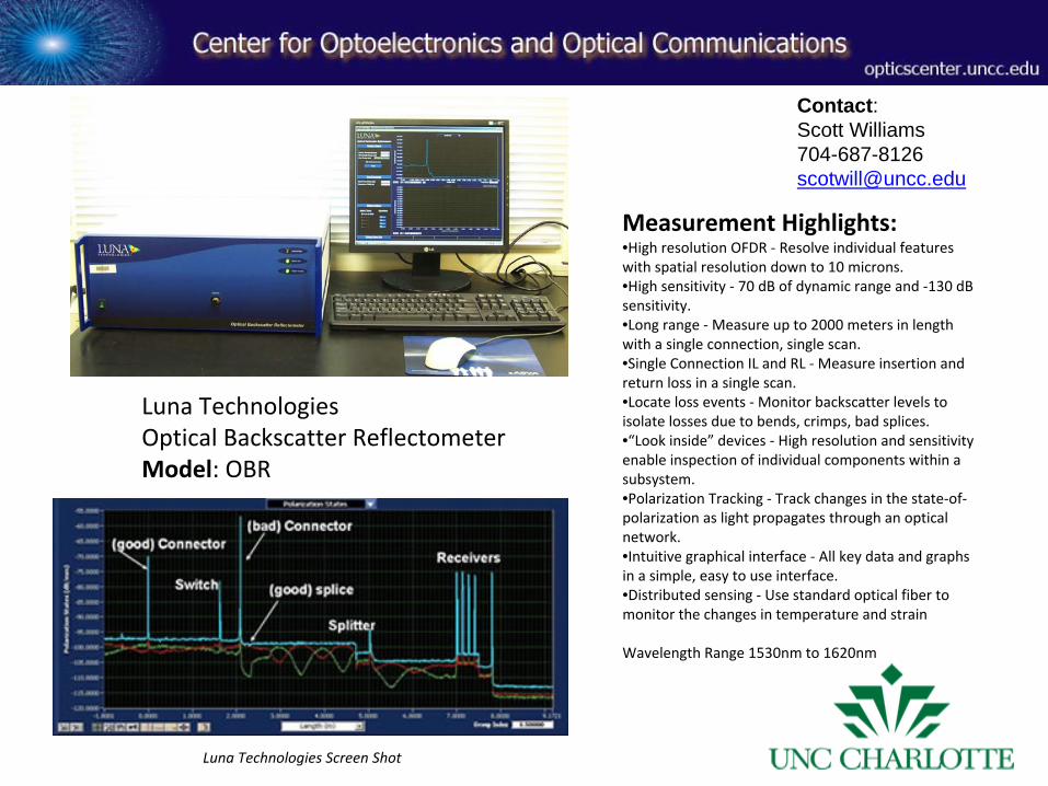
Luna TechnologiesOptical Backscatter ReflectometerModel: OBR
Measurement Highlights:•High resolution OFDR ‐
Resolve individual features
with spatial resolution down to 10 microns.•High sensitivity ‐
70 dB of dynamic range and ‐130 dB
sensitivity.•Long range ‐
Measure up to 2000 meters in length
with a single connection, single scan.•Single Connection IL and RL ‐
Measure insertion and
return loss in a single scan.•Locate loss events ‐
Monitor backscatter levels to
isolate losses due to bends, crimps, bad splices.•“Look inside”
devices ‐
High resolution and sensitivity
enable inspection of individual components within a
subsystem.•Polarization Tracking ‐
Track changes in the state‐of‐
polarization as light propagates through an optical
network.•Intuitive graphical interface ‐
All key data and graphs
in a simple, easy to use interface.•Distributed sensing ‐
Use standard optical fiber to
monitor the changes in temperature and strain
Wavelength Range 1530nm to 1620nm
Luna Technologies Screen Shot
Contact: Scott Williams 704-687-8126 [email protected]
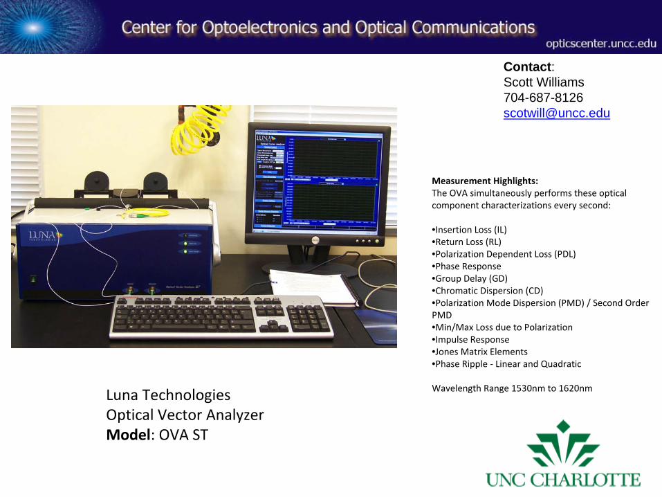
Luna TechnologiesOptical Vector AnalyzerModel: OVA ST
Measurement Highlights:The OVA simultaneously performs these optical
component characterizations every second:
•Insertion Loss (IL)•Return Loss (RL)•Polarization Dependent Loss (PDL)•Phase Response•Group Delay (GD)•Chromatic Dispersion (CD)•Polarization Mode Dispersion (PMD) / Second Order
PMD•Min/Max Loss due to Polarization•Impulse Response•Jones Matrix Elements•Phase Ripple ‐
Linear and Quadratic
Wavelength Range 1530nm to 1620nm

Contact: Scott Williams 704-687-8126 [email protected]
AgilentAll Parameter AnalyzerModel: 81910A
Measurement Highlights:The Agilent 81910A enables exhaustive analysis of
advanced photonic devices, covering all physical
properties relevant to DWDM components in a single
solution:Simultaneous all‐optical measurement of: •(IL) Insertion loss •(RL) Return Loss •(PDL) Polarization Dependent Loss •(GD) Group Delay•(DGD) Differential Group Delay•(CD) Chromatic Dispersion•(PMD) Polarization Mode Dispersion
Direct access to Mueller Matrix and Jones Matrix for
deepest insight into a device's transmission and
reflection properties
Wavelength Range 1530nm to 1620nm

Contact: Scott Williams 704-687-8126 [email protected]
Exfo/BurleighNano Robot SystemModel: FR3000
Features and Benefits
Nano Robot System•Ultrahigh performance in six degrees of freedom
for the most demanding photonics applications• Robust design suitable for the manufacturing floor
as well as labs and clean rooms• High stiffness and stability minimize drift during
bonding and reduce effects of environmental
vibration and temperature• Independent axis control with full range of motion
in six degrees of freedom eliminates detrimental
translation and cross‐
coupling effects•Incorporates patented INCHWORM®
motor
technology to deliver high 0.1‐nm resolution and
long travel
NovacureTypical power output with a standard filter at 320‐
500nm: 23,400 mW/cm2
EFOSUV Curing SystemModel: Novacure
Including
Contact: Scott Williams 704-687-8126 [email protected]
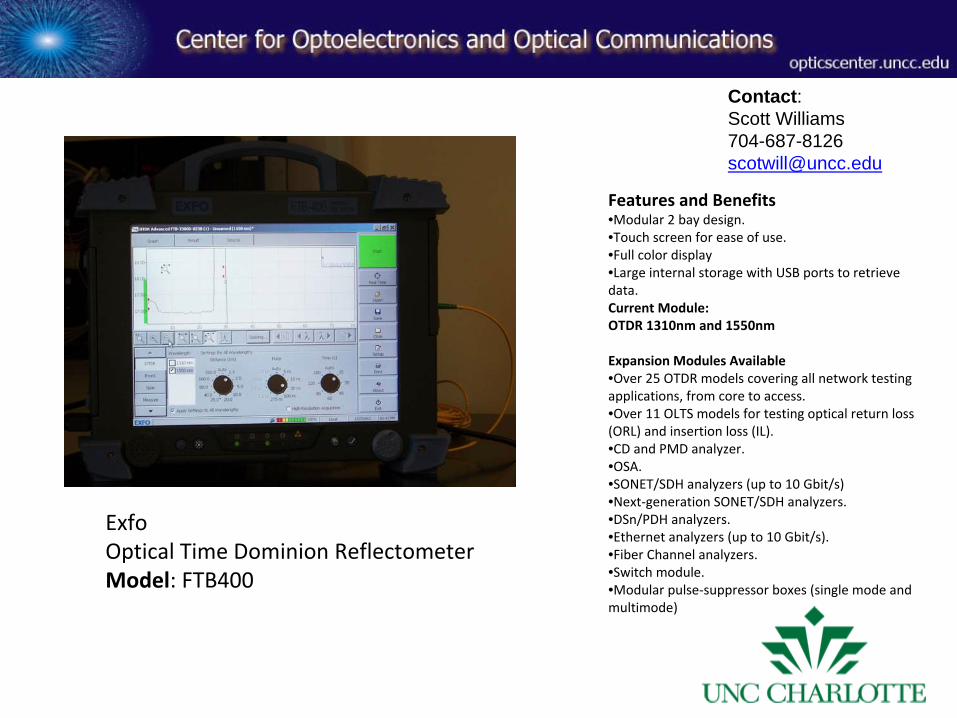
ExfoOptical Time Dominion ReflectometerModel: FTB400
Features and Benefits•Modular 2 bay design.•Touch screen for ease of use.•Full color display•Large internal storage with USB ports to retrieve
data.Current Module:OTDR 1310nm and 1550nm
Expansion Modules Available•Over 25 OTDR models covering all network testing
applications, from core to access.•Over 11 OLTS models for testing optical return loss
(ORL) and insertion loss (IL).•CD and PMD analyzer.•OSA.•SONET/SDH analyzers (up to 10 Gbit/s) •Next‐generation SONET/SDH analyzers.•DSn/PDH analyzers.•Ethernet analyzers (up to 10 Gbit/s).•Fiber Channel analyzers.•Switch module.•Modular pulse‐suppressor boxes (single mode and
multimode)

Contact: Scott Williams 704-687-8126 [email protected]
Bench Top Equipment and Custom Designed Test Arrangements
Capabilities•Multiple Tunable Lasers covering from the S‐Band
through the C & L Bands.•Wavelength Meters•Power Meters•Optical Spectrum Analyzers•Optical Stages •Motion Controllers•Polarization Controllers•Laser Drivers•Free space optical meters and heads•Optical Switches•Erbium Doped Fiber Amplifiers•Microscopes
Contact: Scott Williams 704-687-8126 [email protected]
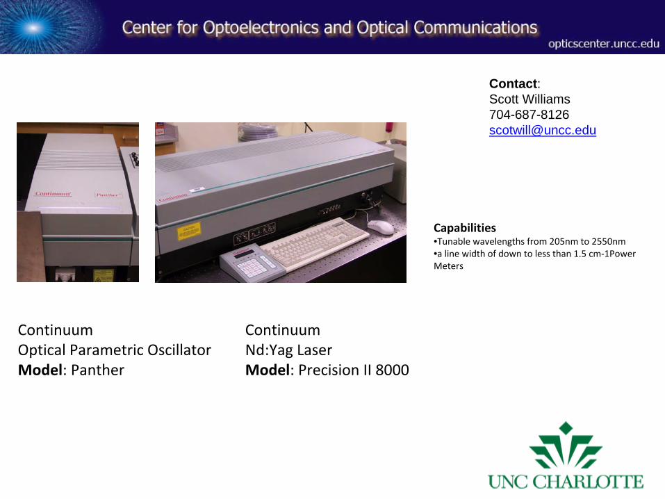
Capabilities•Tunable wavelengths from 205nm to 2550nm•a line width of down to less than 1.5 cm‐1Power
Meters
ContinuumOptical Parametric OscillatorModel: Panther
ContinuumNd:Yag LaserModel: Precision II 8000

Contact: Scott Williams 704-687-8126 [email protected]
Capabilities•1‐15Hz adjustable repetition rates•Up to 100mJ at 15Hz •1064, 532, 355, and 266nm
ContinuumNd:Yag LaserModel: MiniLite II