Product Specification nRF2402 2 2 - Home - Ultra Low … SPECIFICATION nRF2402 Single Chip 2.4 GHz...
33
PRODUCT SPECIFICATION Nordic Semiconductor ASA - Vestre Rosten 81, N-7075 Tiller, Norway - Phone +4772898900 - Fax +4772898989 Revision: 2.2 Page 1 of 33 May 2006 Single chip 2.4 GHz Transmitter FEATURES APPLICATIONS • True single chip GFSK transmitter in a small 16-pin package (QFN16 4x4) • Wireless mouse, keyboard, joystick • Keyless entry • Adjustable output power up to 0dBm • Wireless data communication • Data rate 0 to 1Mbps • Alarm and security systems • Low Bill of Material • Home Automation • Multi Channel operation • 128 channels • Support frequency hopping • Channel switching time <200µs. • Remote control • Surveillance • Automotive • Telemetry • Power supply range: 1.9 to 3.6 V • CRC computation • Intelligent sports equipment • Industrial sensors • ShockBurst™ mode for ultra-low power operation • Toys • Low supply current, typical 10mA peak @ -5dBm output power • 100% RF tested • World wide use GENERAL DESCRIPTION nRF2402 is a single-chip radio transmitter for the world wide 2.4 - 2.5 GHz ISM band. The transmitter consists of a fully integrated frequency synthesizer, a power amplifier, a crystal oscillator and a modulator. Output power and frequency channel is easily programmable by use of the 3-wire interface. Current consumption is very low, only 10 mA at an output power of -5dBm. Built-in ShockBurst™ and Power Down modes make power saving easily realizable. QUICK REFERENCE DATA Parameter Value Unit Minimum supply voltage 1.9 V Maximum output power 0 dBm Maximum GFSK data rate 1000 kbps Supply current GFSK transmitter @ -5dBm output power 10 mA Supply current in Power Down mode 200 nΑ Table 1 nRF2402 quick reference data nRF2402
Transcript of Product Specification nRF2402 2 2 - Home - Ultra Low … SPECIFICATION nRF2402 Single Chip 2.4 GHz...
PRODUCT SPECIFICATION
Nordic Semiconductor ASA - Vestre Rosten 81, N-7075 Tiller, Norway - Phone +4772898900 - Fax +4772898989 Revision: 2.2 Page 1 of 33 May 2006
Single chip 2.4 GHz Transmitter
FEATURES
APPLICATIONS
• True single chip GFSK transmitter in a small 16-pin package (QFN16 4x4)
• Wireless mouse, keyboard, joystick • Keyless entry
• Adjustable output power up to 0dBm • Wireless data communication • Data rate 0 to 1Mbps • Alarm and security systems • Low Bill of Material • Home Automation
• Multi Channel operation • 128 channels • Support frequency hopping • Channel switching time <200µs.
• Remote control • Surveillance • Automotive • Telemetry
• Power supply range: 1.9 to 3.6 V • CRC computation
• Intelligent sports equipment • Industrial sensors
• ShockBurst™ mode for ultra-low power operation
• Toys
• Low supply current, typical 10mA peak @ -5dBm output power
• 100% RF tested
• World wide use
GENERAL DESCRIPTION nRF2402 is a single-chip radio transmitter for the world wide 2.4 - 2.5 GHz ISM band. The transmitter consists of a fully integrated frequency synthesizer, a power amplifier, a crystal oscillator and a modulator. Output power and frequency channel is easily programmable by use of the 3-wire interface. Current consumption is very low, only 10 mA at an output power of -5dBm. Built-in ShockBurst™ and Power Down modes make power saving easily realizable. QUICK REFERENCE DATA Parameter Value Unit Minimum supply voltage 1.9 V
Maximum output power 0 dBm Maximum GFSK data rate 1000 kbps Supply current GFSK transmitter @ -5dBm output power 10 mA Supply current in Power Down mode 200 nΑ
Table 1 nRF2402 quick reference data
nRF2402

PRODUCT SPECIFICATION nRF2402 Single Chip 2.4 GHz Radio Transmitter
Nordic Semiconductor ASA - Vestre Rosten 81, N-7075 Tiller, Norway - Phone +4772898900 - Fax +4772898989 Revision: 2.2 Page 2 of 33 May 2006
BLOCK DIAGRAM
VD
D (13)
XC1 (7)
VS
S (5)
IREF (14)
VDD_PA (12)
VSS_PA (9)
PA
FrequencySynthesiser
VD
D (8)
XC2 (6)
ANT1 (10)
ANT2 (11)
22kΩ
FIFOIn
CRCCode
ShockBurstTM
DIN (4)
CLK (3)
CS (2)
3-wireInterface
PWR_UP (16)
CE (1)
3-wireProgramming
Interface
GFSKFilter
VS
S (15)
Figure 1 nRF2402 with external components.
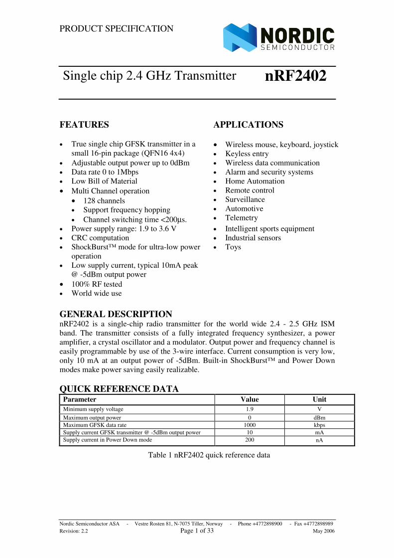
PIN FUNCTIONS Pin Name Pin function Description
1 CE Input Chip Enable Activates TX mode 2 CS Input Chip Select Activates Configuration Mode 3 CLK Input Clock Input TX Data and 3-wire Interface 4 DIN Input TX Data Input / Configuration Data Input 5 VSS Power Ground (0V) 6 XC2 Output Crystal pin 2 7 XC1 Input Crystal pin 1 8 VDD Power Power Supply (1.9-3.6V) 9 VSS_PA Power Ground (0V) 10 ANT1 Power/RF Antenna output 1 11 ANT2 Power/RF Antenna output 2 12 VDD_PA Power Output Power Supply (+1.8V) output to internal Power Amplifier 13 VDD Power Power Supply (1.9-3.6V) 14 IREF Input Reference current 15 VSS Power Ground (0V) 16 PWR_UP Input Power Up
Table 2 nRF2402 pin functions
PRODUCT SPECIFICATION nRF2402 Single Chip 2.4 GHz Radio Transmitter
Nordic Semiconductor ASA - Vestre Rosten 81, N-7075 Tiller, Norway - Phone +4772898900 - Fax +4772898989 Revision: 2.2 Page 3 of 33 May 2006
PIN ASSIGNMENT
CE
CLK
CS
VSS VDD
DIN
XC1
nRF2402
QFN16 4x4
VDD
ANT2
PWR_UP
VDD_PA
VSS_PA
XC2
ANT1
VSS
IREF
15 14 1316
8765
4
3
2
1 12
11
10
9
Figure 2 nRF2402 pin assignment (top view).
PRODUCT SPECIFICATION nRF2402 Single Chip 2.4 GHz Radio Transmitter
Nordic Semiconductor ASA - Vestre Rosten 81, N-7075 Tiller, Norway - Phone +4772898900 - Fax +4772898989 Revision: 2.2 Page 4 of 33 May 2006
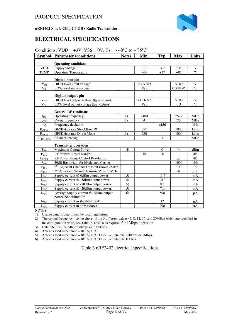
ELECTRICAL SPECIFICATIONS Conditions: VDD = +3V, VSS = 0V, TA = - 40ºC to + 85ºC
Symbol Parameter (condition) Notes Min. Typ. Max. Units
Operating conditions VDD Supply voltage 1.9 3.0 3.6 V
TEMP Operating Temperature -40 +27 +85 ºC
Digital input pin VIH HIGH level input voltage 0.7·VDD VDD V VIL LOW level input voltage Vss 0.3·VDD V
Digital output pin
VOH HIGH level output voltage (IOH=-0.5mA) VDD- 0.3 VDD V VOL LOW level output voltage (IOL=0.5mA) Vss 0.3 V
General RF conditions fOP Operating frequency 1) 2400 2527 MHz
fXTAL Crystal frequency 2) 4 20 MHz ∆f Frequency deviation ±156 kHz
RGFSK GFSK data rate ShockBurst™ >0 1000 kbps RGFSK GFSK data rate Direct Mode 3) 250 1000 kbps
FCHANNEL Channel spacing 1 MHz
Transmitter operation PRF Maximum Output Power 4) 0 +4 dBm PRFC RF Power Control Range 16 20 dB PRFCR RF Power Range Control Resolution ±3 dB PBW 20dB Bandwidth for Modulated Carrier 1000 kHz PRF2 2nd Adjacent Channel Transmit Power 2MHz -20 dBc PRF3 3rd Adjacent Channel Transmit Power 3MHz -40 dBc IVDD Supply current @ 0dBm output power 5) 11.5 mA IVDD Supply current @ -5dBm output power 5) 10.0 mA IVDD Supply current @ -10dBm output power 5) 8.5 mA IVDD Supply current @ -20dBm output power 5) 7.0 mA IVDD Average Supply current @ -5dBm output
power, ShockBurst™ 6) 500 µA
IVDD Supply current in stand-by mode 12 µA IVDD Supply current in power down 200 nA
NOTES: 1) Usable band is determined by local regulations 2) The crystal frequency may be chosen from 5 different values (4, 8, 12, 16, and 20MHz) which are specified in
the configuration word, see Table 7. 16MHz is required for 1Mbps operation. 3) Data rate must be either 250kbps or 1000kbps. 4) Antenna load impedance = 100Ω+j175Ω 5) Antenna load impedance = 100Ω+j175Ω. Effective data rate 250kbps or 1Mbps. 6) Antenna load impedance = 100Ω+j175Ω. Effective data rate 10kbps.
Table 3 nRF2402 electrical specifications

PRODUCT SPECIFICATION nRF2402 Single Chip 2.4 GHz Radio Transmitter
Nordic Semiconductor ASA - Vestre Rosten 81, N-7075 Tiller, Norway - Phone +4772898900 - Fax +4772898989 Revision: 2.2 Page 5 of 33 May 2006
PACKAGE OUTLINE nRF2402G, uses the QFN16 4x4 package, with matt tin plating. The nRF2402 complies with the EU directives WEEE (Waste Electrical and Electronic Equipment), and RoHS (Restriction of use of Certain Hazardous Substances) and also the “green partner” program of SONY, SS-00259.
PRODUCT SPECIFICATION nRF2402 Single Chip 2.4 GHz Radio Transmitter
Nordic Semiconductor ASA - Vestre Rosten 81, N-7075 Tiller, Norway - Phone +4772898900 - Fax +4772898989 Revision: 2.2 Page 6 of 33 May 2006
Package Type A A1 A3 K D/E e D2/E2 L b SAW
QFN16 (4x4 mm)
Min Typ. Max
0.80 0.85 0.90
0.00 0.02 0.05
0.20 REF.
0.20 min
4.0
BSC1
0.65 BSC
2.00 2.10 2.20
0.45 0.50 0.55
0.25 0.30 0.35
Figure 3 nRF2402 Package outline, dimensions in mm.
1 BSC: Basic Spacing between Centers, ref. JEDEC standard 95, page 4.17-11/A
PRODUCT SPECIFICATION nRF2402 Single Chip 2.4 GHz Radio Transmitter
Nordic Semiconductor ASA - Vestre Rosten 81, N-7075 Tiller, Norway - Phone +4772898900 - Fax +4772898989 Revision: 2.2 Page 7 of 33 May 2006
Package marking:
Abbreviations: B – Build Code, i.e. unique code for production sites,
package type and test platform X – "X" grade, i.e. Engineering Samples (optional) YY – 2 digit Year number WW – 2 digit Week number LL – 2 letter wafer lot number code
Ordering Information
Ordering code Description Package Container MOQ1 nRF2402G-REEL 1 Mbps Transmitter 16 pin QFN 4x4 Tape and reel2 4000
nRF2402G-REEL7 1 Mbps Transmitter 16 pin QFN 4x4 Tape and reel3 1500 nRF2402G 1 Mbps Transmitter 16 pin QFN 4x4 Tray 490
nRF2402G-EVKIT Evaluation kit N/A N/A 1
Table nRF2402 ordering information
1 MOQ = Minimum order quantity 2 Moisture Sensitivity Level: MSL2@260ºC, three times reflow
n R F B X 2 4 0 2 G Y Y W W L L

PRODUCT SPECIFICATION nRF2402 Single Chip 2.4 GHz Radio Transmitter
Nordic Semiconductor ASA - Vestre Rosten 81, N-7075 Tiller, Norway - Phone +4772898900 - Fax +4772898989 Revision: 2.2 Page 8 of 33 May 2006
ABSOLUTE MAXIMUM RATINGS Supply voltages VDD............................- 0.3V to + 3.6V VSS .................................................. 0V Input voltage VI....................... - 0.3V to VDD + 0.3V Output voltage VO...................... - 0.3V to VDD + 0.3V
Total Power Dissipation PD (TA=85°C) ............................. 35mW Temperatures Operating Temperature…. - 40°C to + 85°C Storage Temperature…... - 40°C to + 125°C Note: Stress exceeding one or more of the limiting values may cause permanent damage to the device. ATTENTION! Electrostatic Sensitive Device Observe Precaution for handling.
PRODUCT SPECIFICATION nRF2402 Single Chip 2.4 GHz Radio Transmitter
Nordic Semiconductor ASA - Vestre Rosten 81, N-7075 Tiller, Norway - Phone +4772898900 - Fax +4772898989 Revision: 2.2 Page 9 of 33 May 2006
GLOSSARY OF TERMS
Term Description CLK Clock CRC Cyclic Redundancy Check CS Chip Select CE Chip Enable GFSK Gaussian Frequency Shift Keying ISM Industrial-Scientific-Medical MCU Micro Controller Unit OD Overdrive PWR_DWN Power Down PWR_UP Power Up RX Receive ST_BY Standby TX Transmit
Table 4 Glossary
PRODUCT SPECIFICATION nRF2402 Single Chip 2.4 GHz Radio Transmitter
Nordic Semiconductor ASA - Vestre Rosten 81, N-7075 Tiller, Norway - Phone +4772898900 - Fax +4772898989 Revision: 2.2 Page 10 of 33 May 2006
MODES OF OPERATION
Overview of Operational Modes The nRF2402 can be set in the following main modes depending on three control pins:
Mode PWR_UP CE CS Active 1 1 0 Configuration 1 0 1 Stand By 1 0 0 Power Down 0 X X
Table 5 Overview of Operational Modes of nRF2402.
Active Modes The nRF2402 has two transmit modes:
• ShockBurst™ • Direct Mode
The device functionality in these modes is determined by the content of a configuration word. This configuration word is presented in the configuration section.
ShockBurst™ The ShockBurst™ technology uses on-chip FIFO to clock in data at a low data rate and transmit at a very high rate thus enabling extreme reduction in power consumption. When operating the nRF2402 (in co-operation with nRF2401/nRF24E1) in ShockBurst™, you gain access to the high data rates (1 Mbps) offered by the 2.4 GHz band without the need of a costly, high-speed micro controller (MCU) for data processing. By putting all high speed signal processing related to RF protocol on-chip, the nRF2402 offers the following benefits:
• Highly reduced current consumption • Lower system cost (facilitates use of less expensive micro controller) • Greatly reduced risk of ‘on-air’ collisions due to short transmission time
The nRF2402 can be programmed using a simple 3-wire interface where the data rate is decided by the speed of the micro controller. By allowing the digital part of the application to run at low speed while maximizing the data rate on the RF link, the nRF ShockBurst™ mode reduces the average current consumption in applications considerably.
PRODUCT SPECIFICATION nRF2402 Single Chip 2.4 GHz Radio Transmitter
Nordic Semiconductor ASA - Vestre Rosten 81, N-7075 Tiller, Norway - Phone +4772898900 - Fax +4772898989 Revision: 2.2 Page 11 of 33 May 2006
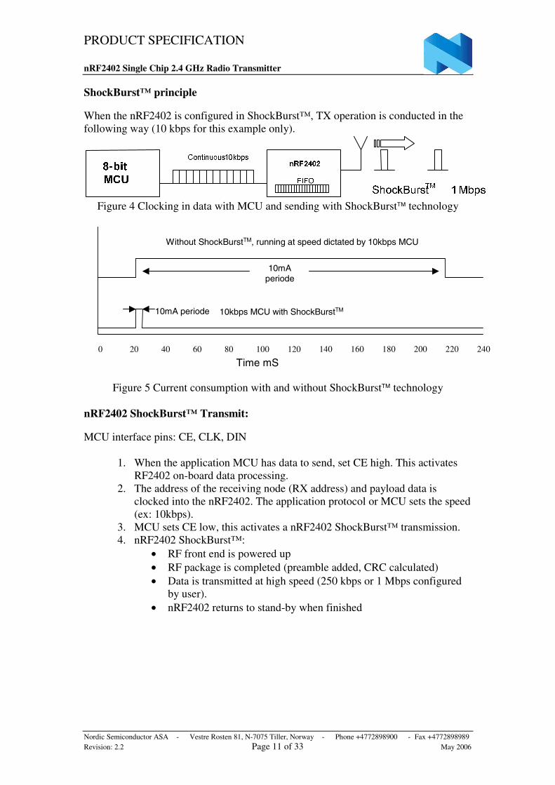
ShockBurst™ principle When the nRF2402 is configured in ShockBurst™, TX operation is conducted in the following way (10 kbps for this example only).
Figure 4 Clocking in data with MCU and sending with ShockBurst technology
Time mS0 20 40 60 80 100 120 140 160 180 200 220 240
10mAperiode
10mA periode
Without ShockBurstTM, running at speed dictated by 10kbps MCU
10kbps MCU with ShockBurstTM
Figure 5 Current consumption with and without ShockBurst technology nRF2402 ShockBurst™ Transmit: MCU interface pins: CE, CLK, DIN
1. When the application MCU has data to send, set CE high. This activates RF2402 on-board data processing.
2. The address of the receiving node (RX address) and payload data is clocked into the nRF2402. The application protocol or MCU sets the speed (ex: 10kbps).
3. MCU sets CE low, this activates a nRF2402 ShockBurst™ transmission. 4. nRF2402 ShockBurst™:
• RF front end is powered up • RF package is completed (preamble added, CRC calculated) • Data is transmitted at high speed (250 kbps or 1 Mbps configured
by user). • nRF2402 returns to stand-by when finished
PRODUCT SPECIFICATION nRF2402 Single Chip 2.4 GHz Radio Transmitter
Nordic Semiconductor ASA - Vestre Rosten 81, N-7075 Tiller, Norway - Phone +4772898900 - Fax +4772898989 Revision: 2.2 Page 12 of 33 May 2006
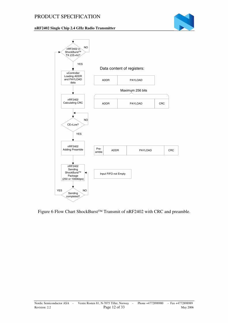
uControllerLoading ADDRand PAYLOAD
data
nRF2402Calculating CRC
ADDR PAYLOAD
ADDR PAYLOAD CRC
Data content of registers:
nRF2402 inShockBurstTM
TX (CE=hi)?
YES
Maximum 256 bits
nRF2402Adding Preamble
nRF2402Sending
ShockBurstTM
Package(250 or 1000kbps)
Pre-amble
ADDR PAYLOAD CRC
Sendingcompleted?
YES NO
CE=Low?
YES
NO
Input FIFO not Empty
NO
Figure 6 Flow Chart ShockBurst™ Transmit of nRF2402 with CRC and preamble.
PRODUCT SPECIFICATION nRF2402 Single Chip 2.4 GHz Radio Transmitter
Nordic Semiconductor ASA - Vestre Rosten 81, N-7075 Tiller, Norway - Phone +4772898900 - Fax +4772898989 Revision: 2.2 Page 13 of 33 May 2006
Direct Mode In direct mode the nRF2402 works like a traditional RF device. The data rate must be 1Mbps ±200ppm, or 250kbps ±200ppm at low data rate setting, for the receiver (nRF2401A/nRF24E1) to detect the signals. MCU interface pins: CE, DIN
1. When application MCU has data to send, set CE high 2. The nRF2402 RF front end is now immediately activated, and after 200 µs
settling time, signal on the DIN pin will modulate the carrier directly. 3. All RF protocol parts must hence be implemented in MCU firmware
(preamble, address and CRC).
Configuration Mode In configuration mode a configuration word of up to 20 bits is downloaded to nRF2402. This is done through a simple 3-wire interface (CS, CLK and DIN). For more information on configuration please refer to the nRF2402 device configuration chapter, page14.
Power Down Mode Power down mode is used to achieve very low current consumption. Effectively the chip is disabled with minimal leakage current consumption, typically less than 200nA. Operating in this mode when not transmitting data significantly increases battery lifetime. Stand-By Mode Stand by mode is used to achieve low current consumption. In this mode only a part of the crystal oscillator is running (12µA) to guarantee a short start-up time. Operating in this mode when not transmitting data increases battery lifetime while keeping start up delays short.
Pin configuration for the different modes of nRF2402
nRF2402 MODES INPUT PINS Pin Name PWR_UP CE CS CLK DIN
Power down 0 0 X X X Stand by 1 0 0 X X Configuration 1 0 1 CLK CONFIG DATA TX ShockBurst™ 1 1 0 CLK TX DATA TX Direct 1 1 0 Set to 0∗ TX DATA
Table 6 Pin configuration of nRF2402.
∗ CLK not used in direct mode.
PRODUCT SPECIFICATION nRF2402 Single Chip 2.4 GHz Radio Transmitter
Nordic Semiconductor ASA - Vestre Rosten 81, N-7075 Tiller, Norway - Phone +4772898900 - Fax +4772898989 Revision: 2.2 Page 14 of 33 May 2006
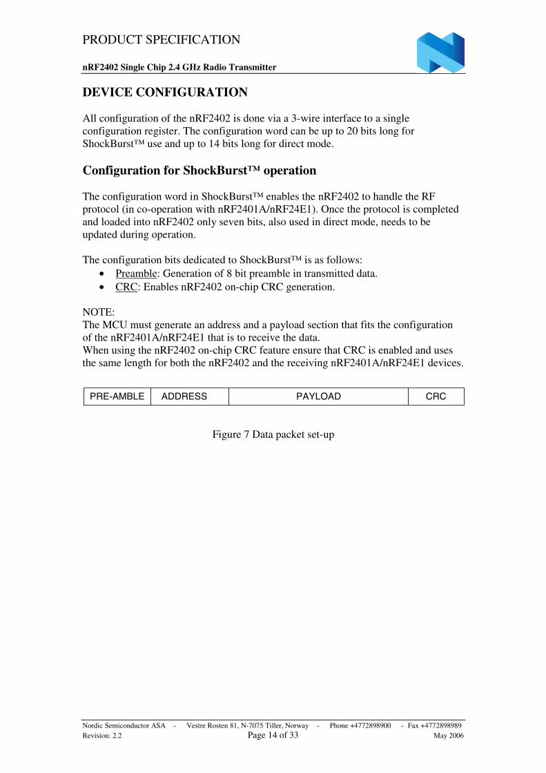
DEVICE CONFIGURATION All configuration of the nRF2402 is done via a 3-wire interface to a single configuration register. The configuration word can be up to 20 bits long for ShockBurst™ use and up to 14 bits long for direct mode. Configuration for ShockBurst™ operation The configuration word in ShockBurst™ enables the nRF2402 to handle the RF protocol (in co-operation with nRF2401A/nRF24E1). Once the protocol is completed and loaded into nRF2402 only seven bits, also used in direct mode, needs to be updated during operation. The configuration bits dedicated to ShockBurst™ is as follows:
• Preamble: Generation of 8 bit preamble in transmitted data. • CRC: Enables nRF2402 on-chip CRC generation.
NOTE: The MCU must generate an address and a payload section that fits the configuration of the nRF2401A/nRF24E1 that is to receive the data. When using the nRF2402 on-chip CRC feature ensure that CRC is enabled and uses the same length for both the nRF2402 and the receiving nRF2401A/nRF24E1 devices.
PRE-AMBLE ADDRESS PAYLOAD CRC
Figure 7 Data packet set-up
PRODUCT SPECIFICATION nRF2402 Single Chip 2.4 GHz Radio Transmitter
Nordic Semiconductor ASA - Vestre Rosten 81, N-7075 Tiller, Norway - Phone +4772898900 - Fax +4772898989 Revision: 2.2 Page 15 of 33 May 2006
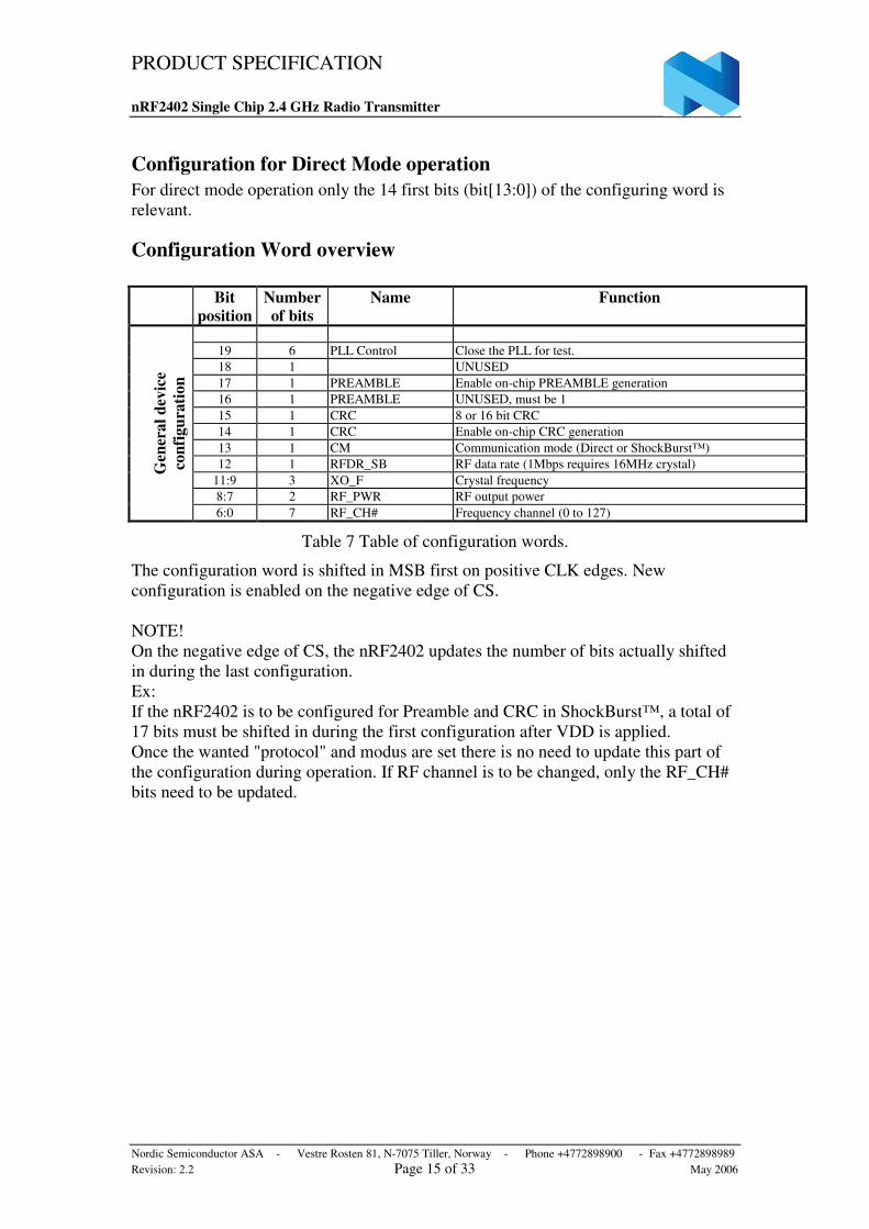
Configuration for Direct Mode operation For direct mode operation only the 14 first bits (bit[13:0]) of the configuring word is relevant.
Configuration Word overview
Bit position
Number of bits
Name Function
19 6 PLL Control Close the PLL for test. 18 1 UNUSED 17 1 PREAMBLE Enable on-chip PREAMBLE generation 16 1 PREAMBLE UNUSED, must be 1 15 1 CRC 8 or 16 bit CRC 14 1 CRC Enable on-chip CRC generation 13 1 CM Communication mode (Direct or ShockBurst™) 12 1 RFDR_SB RF data rate (1Mbps requires 16MHz crystal)
11:9 3 XO_F Crystal frequency 8:7 2 RF_PWR RF output power
G
ener
al d
evic
e co
nfig
urat
ion
6:0 7 RF_CH# Frequency channel (0 to 127)
Table 7 Table of configuration words.
The configuration word is shifted in MSB first on positive CLK edges. New configuration is enabled on the negative edge of CS. NOTE! On the negative edge of CS, the nRF2402 updates the number of bits actually shifted in during the last configuration. Ex: If the nRF2402 is to be configured for Preamble and CRC in ShockBurst™, a total of 17 bits must be shifted in during the first configuration after VDD is applied. Once the wanted "protocol" and modus are set there is no need to update this part of the configuration during operation. If RF channel is to be changed, only the RF_CH# bits need to be updated.

PRODUCT SPECIFICATION nRF2402 Single Chip 2.4 GHz Radio Transmitter
Nordic Semiconductor ASA - Vestre Rosten 81, N-7075 Tiller, Norway - Phone +4772898900 - Fax +4772898989 Revision: 2.2 Page 16 of 33 May 2006
Configuration Word Detailed Description The following describes the function of the 32 bits (bit 31 = MSB) that is used to configure the nRF2402. General Device Configuration: bit[13:0] ShockBurst™ Configuration: bit[17:14] Test Configuration: bit[19:18]
TEST ShockBurst D19 D18 D17 D16 D15 D14 PLL PRE_EN CRC
0 0 1 1 0 0 Default
RF-Programming LSB
D13 D12 D11 D10 D9 D8 D7 D6 D5 D4 D3 D2 D1 D0 Burst OD XO Frequency RF Power Channel selection
0 0 1 1 1 1 0 0 0 0 0 0 1 0 Default
The MSB bit should be loaded first into the configuration register. Default configuration word: h30F02. Test configuration Bit 19:
PLL: For test purposes the PLL may be closed to send a constant carrier Logic 0: Open loop (normal operation) Logic 1: Closed loop (test only)
Bit: 18: Not used, must be set to logic 1
PRODUCT SPECIFICATION nRF2402 Single Chip 2.4 GHz Radio Transmitter
Nordic Semiconductor ASA - Vestre Rosten 81, N-7075 Tiller, Norway - Phone +4772898900 - Fax +4772898989 Revision: 2.2 Page 17 of 33 May 2006
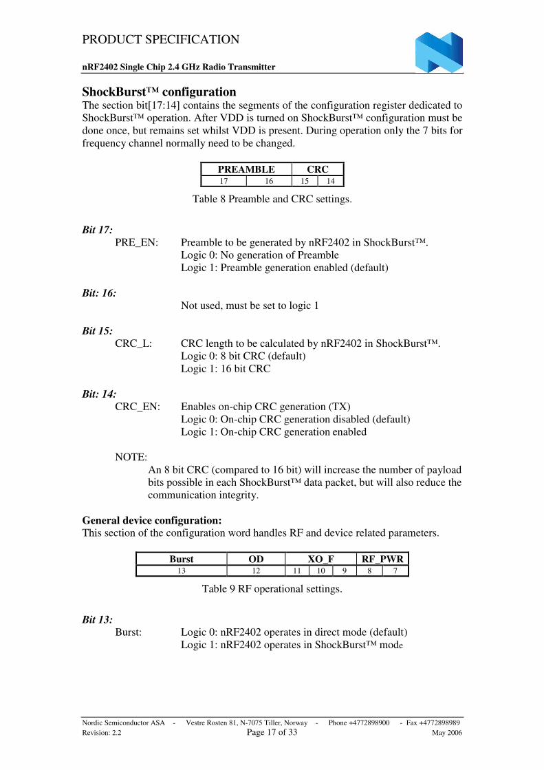
ShockBurst™ configuration The section bit[17:14] contains the segments of the configuration register dedicated to ShockBurst™ operation. After VDD is turned on ShockBurst™ configuration must be done once, but remains set whilst VDD is present. During operation only the 7 bits for frequency channel normally need to be changed.
PREAMBLE CRC 17 16 15 14
Table 8 Preamble and CRC settings.
Bit 17:
PRE_EN: Preamble to be generated by nRF2402 in ShockBurst™. Logic 0: No generation of Preamble Logic 1: Preamble generation enabled (default)
Bit: 16: Not used, must be set to logic 1 Bit 15:
CRC_L: CRC length to be calculated by nRF2402 in ShockBurst™. Logic 0: 8 bit CRC (default) Logic 1: 16 bit CRC
Bit: 14:
CRC_EN: Enables on-chip CRC generation (TX) Logic 0: On-chip CRC generation disabled (default) Logic 1: On-chip CRC generation enabled
NOTE:
An 8 bit CRC (compared to 16 bit) will increase the number of payload bits possible in each ShockBurst™ data packet, but will also reduce the communication integrity.
General device configuration: This section of the configuration word handles RF and device related parameters.
Burst OD XO_F RF_PWR
13 12 11 10 9 8 7
Table 9 RF operational settings.
Bit 13:
Burst: Logic 0: nRF2402 operates in direct mode (default) Logic 1: nRF2402 operates in ShockBurst™ mode

PRODUCT SPECIFICATION nRF2402 Single Chip 2.4 GHz Radio Transmitter
Nordic Semiconductor ASA - Vestre Rosten 81, N-7075 Tiller, Norway - Phone +4772898900 - Fax +4772898989 Revision: 2.2 Page 18 of 33 May 2006
Bit 12: OD: Logic 0: 250 kbps data rate Logic 1: 1 Mbps data rate
NOTE:
1Mbps requires 16MHz crystal. Bit 11-9:
XO_F: Selects the nRF2402 crystal frequency to be used:
XO FREQUENCY SELECTION D11 D10 D9 Crystal Frequency [MHz]
0 0 0 4 0 0 1 8 0 1 0 12 0 1 1 16 1 0 0 20
Table 10 Crystal frequency setting.
Bit 8-7: RF_PWR: Sets nRF2402 RF output power:
RF OUTPUT POWER
D8 D7 P [dBm] 0 0 -20 0 1 -10 1 0 -5 1 1 0
Table 11 RF output power setting.
Conditions: Load impedance = 100+j175 Ω.
RF channel
RF_CH#
6 5 4 3 2 1 0
Table 12 Frequency channel setting.
Bit 6 – 0: RF_CH#: Sets the frequency channel the nRF2402 transmits in.
The channel frequency is given by:
MHzCHRFMHzChannelRF 0.1#_2400 ⋅+=
RF_CH #: Frequencies between 2400MHz and 2527MHz may be set.
PRODUCT SPECIFICATION nRF2402 Single Chip 2.4 GHz Radio Transmitter
Nordic Semiconductor ASA - Vestre Rosten 81, N-7075 Tiller, Norway - Phone +4772898900 - Fax +4772898989 Revision: 2.2 Page 19 of 33 May 2006
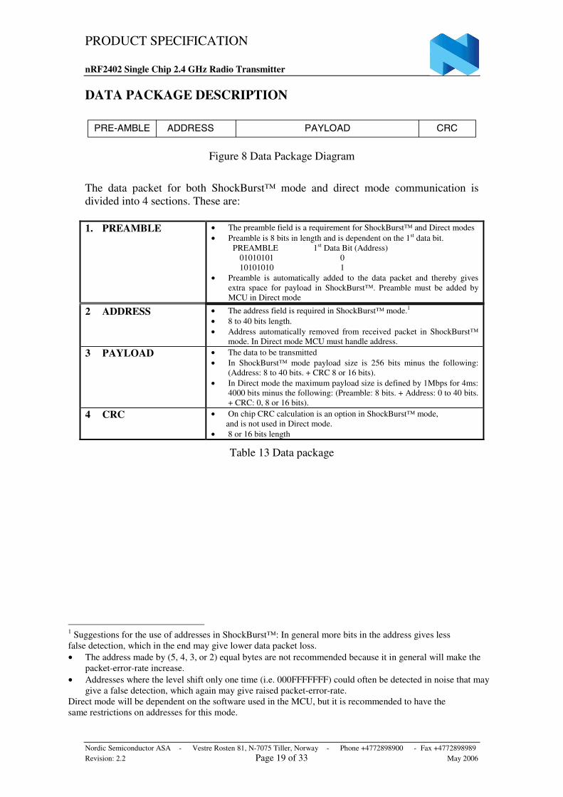
DATA PACKAGE DESCRIPTION
PRE-AMBLE ADDRESS PAYLOAD CRC
Figure 8 Data Package Diagram
The data packet for both ShockBurst™ mode and direct mode communication is divided into 4 sections. These are: 1. PREAMBLE • The preamble field is a requirement for ShockBurst™ and Direct modes
• Preamble is 8 bits in length and is dependent on the 1st data bit. PREAMBLE 1st Data Bit (Address)
01010101 0 10101010 1
• Preamble is automatically added to the data packet and thereby gives extra space for payload in ShockBurst™. Preamble must be added by MCU in Direct mode
2 ADDRESS • The address field is required in ShockBurst™ mode.1 • 8 to 40 bits length. • Address automatically removed from received packet in ShockBurst™
mode. In Direct mode MCU must handle address.
3 PAYLOAD • The data to be transmitted • In ShockBurst™ mode payload size is 256 bits minus the following:
(Address: 8 to 40 bits. + CRC 8 or 16 bits). • In Direct mode the maximum payload size is defined by 1Mbps for 4ms:
4000 bits minus the following: (Preamble: 8 bits. + Address: 0 to 40 bits. + CRC: 0, 8 or 16 bits).
4 CRC • On chip CRC calculation is an option in ShockBurst™ mode, and is not used in Direct mode.
• 8 or 16 bits length
Table 13 Data package
1 Suggestions for the use of addresses in ShockBurst™: In general more bits in the address gives less false detection, which in the end may give lower data packet loss. • The address made by (5, 4, 3, or 2) equal bytes are not recommended because it in general will make the
packet-error-rate increase. • Addresses where the level shift only one time (i.e. 000FFFFFFF) could often be detected in noise that may
give a false detection, which again may give raised packet-error-rate. Direct mode will be dependent on the software used in the MCU, but it is recommended to have the same restrictions on addresses for this mode.
PRODUCT SPECIFICATION nRF2402 Single Chip 2.4 GHz Radio Transmitter
Nordic Semiconductor ASA - Vestre Rosten 81, N-7075 Tiller, Norway - Phone +4772898900 - Fax +4772898989 Revision: 2.2 Page 20 of 33 May 2006
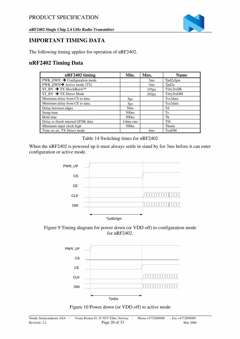
IMPORTANT TIMING DATA The following timing applies for operation of nRF2402.
nRF2402 Timing Data
nRF2402 timing Min. Max. Name PWR_DWN Configuration mode 3ms Tpd2cfgm PWR_DWN Active mode (TX) 3ms Tpd2a ST_BY TX ShockBurst™ 195µs Tsby2txSB ST_BY TX Direct Mode 202µs Tsby2txDM Minimum delay from CS to data. 5µs Tcs2data Minimum delay from CE to data. 5µs Tce2data Delay between edges 50ns Td Setup time 500ns Ts Hold time 500ns Th Delay to finish internal GFSK data 1/data rate Tfd Minimum input clock high 500ns Thmin Time on air, TX Direct mode 4ms ToaDM
Table 14 Switching times for nRF2402
When the nRF2402 is powered up it must always settle in stand by for 3ms before it can enter configuration or active mode.
PWR_UP
DIN
CE
Tpd2cfgm
CLK
CS
Figure 9 Timing diagram for power down (or VDD off) to configuration mode for nRF2402.
PWR_UP
DIN
CE
Tpd2a
CLK
CS
Figure 10 Power down (or VDD off) to active mode
PRODUCT SPECIFICATION nRF2402 Single Chip 2.4 GHz Radio Transmitter
Nordic Semiconductor ASA - Vestre Rosten 81, N-7075 Tiller, Norway - Phone +4772898900 - Fax +4772898989 Revision: 2.2 Page 21 of 33 May 2006
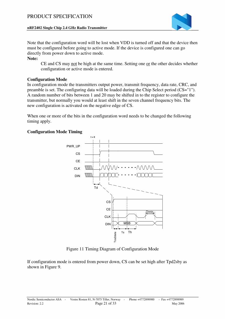
Note that the configuration word will be lost when VDD is turned off and that the device then must be configured before going to active mode. If the device is configured one can go directly from power down to active mode. Note:
CE and CS may not be high at the same time. Setting one or the other decides whether configuration or active mode is entered.
Configuration Mode In configuration mode the transmitters output power, transmit frequency, data rate, CRC, and preamble is set. The configuring data will be loaded during the Chip Select period (CS="1"). A random number of bits between 1 and 20 may be shifted in to the register to configure the transmitter, but normally you would at least shift in the seven channel frequency bits. The new configuration is activated on the negative edge of CS. When one or more of the bits in the configuration word needs to be changed the following timing apply. Configuration Mode Timing
CS
CLK
DIN
CE
PWR_UP
CLK
DIN
CS
MSB
Ts
CE
Th
t = 0
Td
Thmin
Tcs
2dat
a
Figure 11 Timing Diagram of Configuration Mode
If configuration mode is entered from power down, CS can be set high after Tpd2sby as shown in Figure 9.
PRODUCT SPECIFICATION nRF2402 Single Chip 2.4 GHz Radio Transmitter
Nordic Semiconductor ASA - Vestre Rosten 81, N-7075 Tiller, Norway - Phone +4772898900 - Fax +4772898989 Revision: 2.2 Page 22 of 33 May 2006
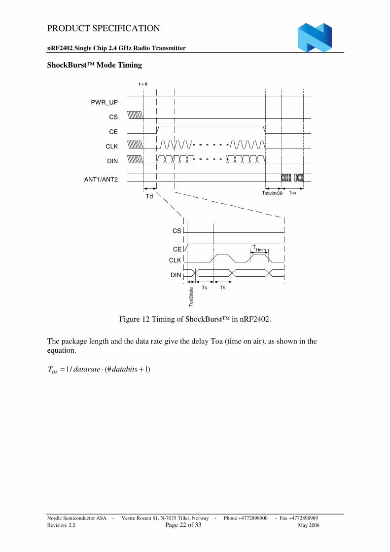
ShockBurst™ Mode Timing
CS
CLK
DIN
CE
PWR_UP
CLK
DIN
CS
Th
Tce
2dat
a
CE
Td
ANT1/ANT2 .
Tsby2txSB Toa
t = 0
THmin
Ts
Figure 12 Timing of ShockBurst™ in nRF2402.
The package length and the data rate give the delay Toa (time on air), as shown in the equation.
)1(#/1 +⋅= databitsdatarateTOA
PRODUCT SPECIFICATION nRF2402 Single Chip 2.4 GHz Radio Transmitter
Nordic Semiconductor ASA - Vestre Rosten 81, N-7075 Tiller, Norway - Phone +4772898900 - Fax +4772898989 Revision: 2.2 Page 23 of 33 May 2006
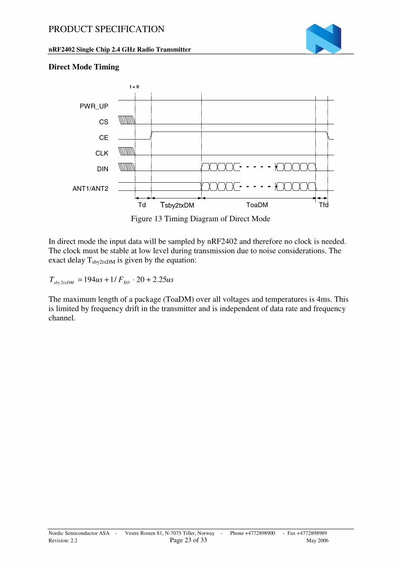
Direct Mode Timing
CS
CLK
DIN
CE
PWR_UP
Td
ANT1/ANT2
Tsby2txDM ToaDM Tfd
t = 0
Figure 13 Timing Diagram of Direct Mode
In direct mode the input data will be sampled by nRF2402 and therefore no clock is needed. The clock must be stable at low level during transmission due to noise considerations. The exact delay Tsby2txDM is given by the equation:
usFusT XOtxDMsby 25.220/11942 +⋅+=
The maximum length of a package (ToaDM) over all voltages and temperatures is 4ms. This is limited by frequency drift in the transmitter and is independent of data rate and frequency channel.

PRODUCT SPECIFICATION nRF2402 Single Chip 2.4 GHz Radio Transmitter
Nordic Semiconductor ASA - Vestre Rosten 81, N-7075 Tiller, Norway - Phone +4772898900 - Fax +4772898989 Revision: 2.2 Page 24 of 33 May 2006
PERIPHERAL RF INFORMATION
Antenna output The ANT1 and ANT2 output pins provide a balanced RF output to the antenna. The pins must have a DC path to VDD_PA, either via a RF choke or via the center point in a balanced antenna. Differential load impedance between the ANT1 and ANT2 pins, 100Ω+j175Ω, is recommended for maximum output power. Antennas with lower load impedance (for example 50Ω) can be matched to nRF2402 by using a simple matching network.
Antenna matching networks The recommended 50Ω matching network is shown in Figure 14. This is a low pass network improving higher harmonic suppression.
3.3nH
5.6nH1.0pF
1.0pF
2.2nF 4.7pF
RF output
10nH
4.7pF
nRF2402ANT1
ANT2
VDD_PA
Figure 14 Low pass antenna matching network
A somewhat simpler matching network is shown in Figure 15.
nRF2402ANT1
ANT2
VDD_PA
4.7pF
3.6nH
22nH
1.0pF
1.0pF
2.2nF
Cout1.5pF
RF output
Figure 15 High pass antenna matching network
This network utilizes one component less and uses few inductors, but performance of this network requires very careful PCB ground plane layout. The value of capacitor Cout is dependent on PCB ground plane layout and parasitics in the layout, and must hence be matched to a given application layout. The value of Cout will typically be in the range 1.0pF – 1.8pF. Cout must be tuned while checking that the harmonics output is below frequency regulatory limits.
PRODUCT SPECIFICATION nRF2402 Single Chip 2.4 GHz Radio Transmitter
Nordic Semiconductor ASA - Vestre Rosten 81, N-7075 Tiller, Norway - Phone +4772898900 - Fax +4772898989 Revision: 2.2 Page 25 of 33 May 2006
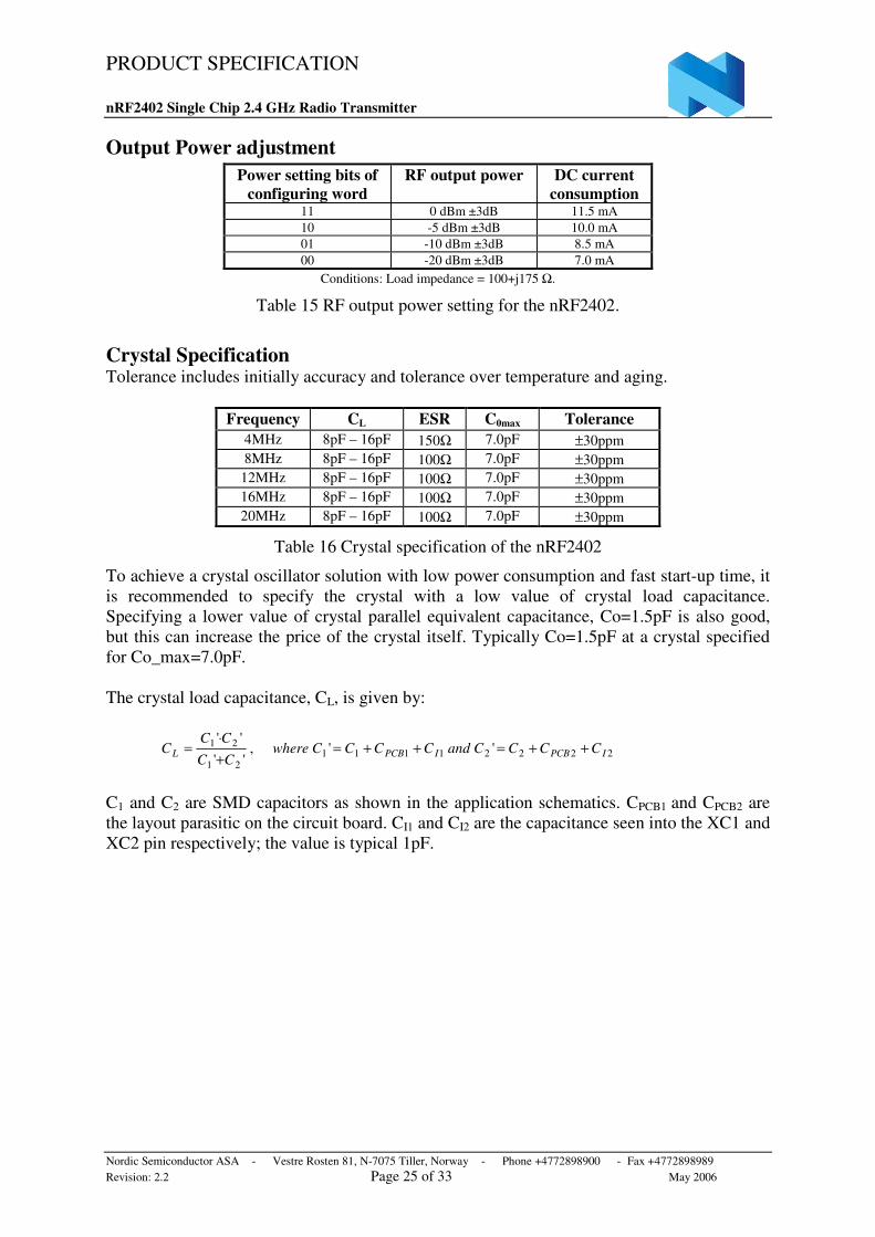
Output Power adjustment Power setting bits of
configuring word RF output power DC current
consumption 11 0 dBm ±3dB 11.5 mA 10 -5 dBm ±3dB 10.0 mA 01 -10 dBm ±3dB 8.5 mA 00 -20 dBm ±3dB 7.0 mA
Conditions: Load impedance = 100+j175 Ω.
Table 15 RF output power setting for the nRF2402.
Crystal Specification Tolerance includes initially accuracy and tolerance over temperature and aging.
Frequency CL ESR C0max Tolerance
4MHz 8pF – 16pF 150Ω 7.0pF ±30ppm 8MHz 8pF – 16pF 100Ω 7.0pF ±30ppm
12MHz 8pF – 16pF 100Ω 7.0pF ±30ppm 16MHz 8pF – 16pF 100Ω 7.0pF ±30ppm 20MHz 8pF – 16pF 100Ω 7.0pF ±30ppm
Table 16 Crystal specification of the nRF2402
To achieve a crystal oscillator solution with low power consumption and fast start-up time, it is recommended to specify the crystal with a low value of crystal load capacitance. Specifying a lower value of crystal parallel equivalent capacitance, Co=1.5pF is also good, but this can increase the price of the crystal itself. Typically Co=1.5pF at a crystal specified for Co_max=7.0pF. The crystal load capacitance, CL, is given by:
2222111121
21 '',''
''IPCBIPCBL CCCCandCCCCwhere
CC
CCC ++=++=
+⋅
=
C1 and C2 are SMD capacitors as shown in the application schematics. CPCB1 and CPCB2 are the layout parasitic on the circuit board. CI1 and CI2 are the capacitance seen into the XC1 and XC2 pin respectively; the value is typical 1pF.

PRODUCT SPECIFICATION nRF2402 Single Chip 2.4 GHz Radio Transmitter
Nordic Semiconductor ASA - Vestre Rosten 81, N-7075 Tiller, Norway - Phone +4772898900 - Fax +4772898989 Revision: 2.2 Page 26 of 33 May 2006
Sharing crystal with micro controller. When using a micro controller to drive the crystal reference input XC1 of the nRF2402 transmitter some rules must be followed.
Crystal parameters: When the micro controller drives the nRF2402 XC1 input, all crystal load parameters (CL, C0, ESR) are set by the micro controller specification. The frequency accuracy (±30 ppm) is still set by the nRF2402 specification. The nRF2402 will load the crystal circuitry of the micro controller by XC1 input capacitance (0.5pF) plus PBC routing parasitic.
External reference input amplitude & Current consumption The reference input should never have signal levels exceeding rail voltages. Exceeding rail voltage will excite the ESD structure and the radio performance is degraded below specification. Applying reference sources without DC bias will bring the reference signal under GND level, and this is not acceptable.
XC1
XO_OUT
Amplitudecontrolled
current source
Buffer:Sine to
full swing
Current starvedinverter:
XOSC core
XC2
Vdd
Vss
Vdd
VssESDESD
Figure 16 Principle of crystal oscillator
It is hence recommended to use a DC-block before the XC1 pin so that the internal ESD structures will self biases the XC1 voltage. The nRF2402 crystal oscillator is amplitude regulated. To achieve low current consumption and also good signal-to-noise ratio, it is recommended to use an input signal larger than 0.4 V-peak. The needed input swing is independent of the crystal frequency. When using external crystal reference, XC2 is not used and can be left as an open pin.
PRODUCT SPECIFICATION nRF2402 Single Chip 2.4 GHz Radio Transmitter
Nordic Semiconductor ASA - Vestre Rosten 81, N-7075 Tiller, Norway - Phone +4772898900 - Fax +4772898989 Revision: 2.2 Page 27 of 33 May 2006
Frequency Reference MCU In direct mode there is a requirement on the accuracy of the data rate. For the receiver to detect the incoming data and recover the clock, the data rate must be within ±200ppm, given that the data is "random", i.e. there is a statistical calculation on how often a preamble like sequence is present in the data. The clock is synchronized for any preamble detection, be it a dedicated preamble or part of the data stream.
PCB layout and de-coupling guidelines A well-designed PCB is necessary to achieve good RF performance. Keep in mind that a poor layout may lead to loss of performance, or even functionality, if due care is not taken. A fully qualified RF-layout for the nRF2402 and its surrounding components, including matching networks, can be downloaded from www.nordicsemi.no. A PCB with a minimum of two layers including a ground plane is recommended for optimum performance. The nRF2402 DC supply voltage should be de-coupled as close as possible to the VDD pins with high performance RF capacitors, see Table 17. It is preferable to mount a large surface mount capacitor (e.g. 4.7µF tantalum) in parallel with the smaller value capacitors. The nRF2402 supply voltage should be filtered and routed separately from the supply voltages of any digital circuitry. Long power supply lines on the PCB should be avoided. All device grounds, VDD connections and VDD bypass capacitors must be connected as close as possible to the nRF2402 IC. The VSS pins should be connected directly to the ground plane. One via hole should be used for each VSS pin. Full swing digital data or control signals should not be routed close to the crystal or the power supply lines.

PRODUCT SPECIFICATION nRF2402 Single Chip 2.4 GHz Radio Transmitter
Nordic Semiconductor ASA - Vestre Rosten 81, N-7075 Tiller, Norway - Phone +4772898900 - Fax +4772898989 Revision: 2.2 Page 28 of 33 May 2006
Reflow information
Figure 17 Soldering reflow profile, GREEN
Ramp rate (RT-150ºC) 1.38 ºC/s Pre-heat (150-200ºC) 134 s Dwell @217ºC 50 s Dwell @245ºC 10 s Ramp up 1.42 ºC/s Ramp down 2.59 ºC/s Peak temperature 257 ºC Time from RT to PT 320 s
PRODUCT SPECIFICATION nRF2402 Single Chip 2.4 GHz Radio Transmitter
Nordic Semiconductor ASA - Vestre Rosten 81, N-7075 Tiller, Norway - Phone +4772898900 - Fax +4772898989 Revision: 2.2 Page 29 of 33 May 2006
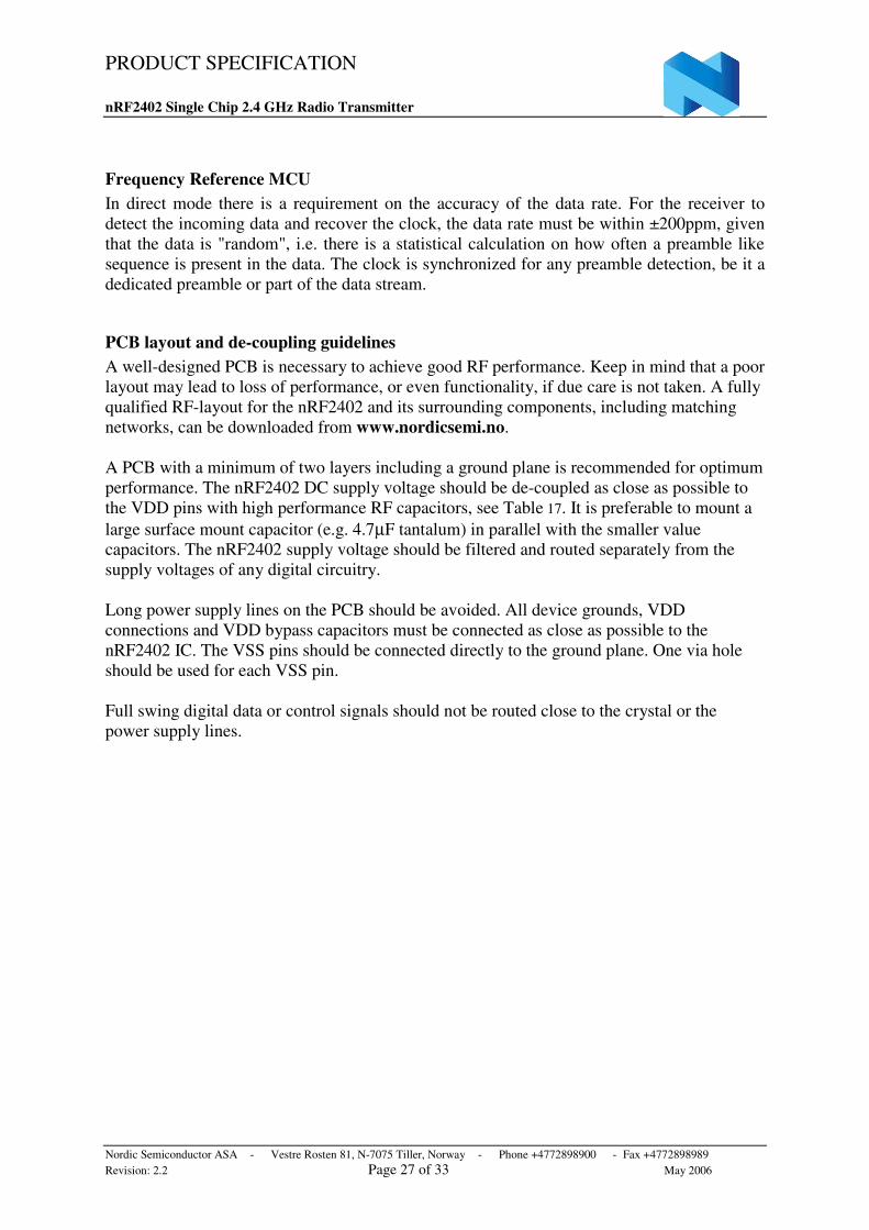
Application example
nRF2402 with single ended matching network
X116MHz
R1
1M
C122pF
C222pF
R222k
C51nF
C610nF
C34.7pF
L13.3nH
L2
10nH
C81.0pF
C71.0pFVDD
VDD
PWR_UPCECS
CLKDIN
C42.2nF
VDD
RF output
C9
4.7pF
L3
5.6nH
VDD_PA12
ANT211
ANT1 10
VSS_PA9
PWR
_U
P16
VSS
15
IRE
F14
VD
D13
CE1
CS2
CLK3
DIN4
VSS
5
XC
26
XC
17
VD
D8
nRF2402
U1NRF2402
Figure 18 nRF2402 schematic for RF layouts with single ended 50Ω antenna
Component Description Size Value Tolerance Units C1 Capacitor ceramic, 50V, NPO 0603 22 ±5% pF C2 Capacitor ceramic, 50V, NPO 0603 22 ±5% pF C3 Capacitor ceramic, 50V, NPO 0603 4.7 ±5% pF C4 Capacitor ceramic, 50V, X7R 0603 2.2 ±10% nF C5 Capacitor ceramic, 50V, X7R 0603 1.0 ±10% nF C6 Capacitor ceramic, 50V, X7R 0603 10 ±10% nF R1 Resistor 0603 1.0 ±10% MΩ R2 Resistor 0603 22 ±1% kΩ U1 nRF2402 transmitter QFN16 / 4x4 nRF2402 X1 Crystal, CL = 12pF,
ESR < 100 ohm LxWxH =
4.0x2.5x0.8 16 1) +/- 30 ppm MHz
L1 Inductor 2) 0603 3.3 ± 5% nH L2 Inductor 2) 0603 10 ± 5% nH L3 Inductor 2) 0603 5.6 ± 5% nH C7 Ceramic capacitor, 50V, NP0 0603 1.0 ± 0.1 pF pF C8 Ceramic capacitor, 50V, NP0 0603 1.0 ± 0.1 pF pF C9 Ceramic capacitor, 50V, NP0 0603 4.7 ± 0.25 pF pF
Table 17 Recommended components (BOM) in nRF2402 with antenna matching network
1) nRF2402 can operate at several crystal frequencies, ref. the Crystal Spec. chapter. 2) Self-resonant frequency (SFR) must be > 2.7 GHz
PRODUCT SPECIFICATION nRF2402 Single Chip 2.4 GHz Radio Transmitter
Nordic Semiconductor ASA - Vestre Rosten 81, N-7075 Tiller, Norway - Phone +4772898900 - Fax +4772898989 Revision: 2.2 Page 30 of 33 May 2006
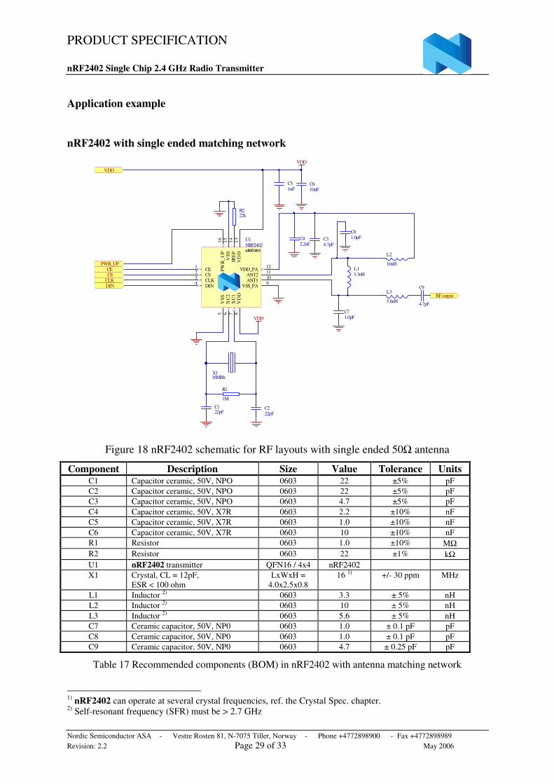
PCB layout example Figure 19 shows a PCB layout example for the application schematic in Figure 18. A double-sided FR-4 board of 1.6mm thickness is used. This PCB has ground planes on both bottom layer and top layer to ensure good grounding of critical component. Additionally, there are ground areas on the component side of the board to ensure sufficient grounding of critical components. A large number of via holes connect the top layer ground areas to the bottom layer ground plane.
Top silk screen
No components in bottom layer
Top view
Bottom view
Figure 19 nRF2402 RF layout with single ended connection to 50Ω antenna and 0603 size passive components

PRODUCT SPECIFICATION nRF2402 Single Chip 2.4 GHz Radio Transmitter
Nordic Semiconductor ASA - Vestre Rosten 81, N-7075 Tiller, Norway - Phone +4772898900 - Fax +4772898989 Revision: 2.2 Page 31 of 33 May 2006
DEFINITIONS
Data sheet status Objective product specification This datasheet contains target specifications for product development. Preliminary product specification
This datasheet contains preliminary data; supplementary data may be published from Nordic Semiconductor ASA later.
Product specification This datasheet contains final product specifications. Nordic Semiconductor ASA reserves the right to make changes at any time without notice in order to improve design and supply the best possible product.
Limiting values Stress above one or more of the limiting values may cause permanent damage to the device. These are stress ratings only and operation of the device at these or at any other conditions above those given in the Specifications sections of the specification is not implied. Exposure to limiting values for extended periods may affect device reliability.
Application information Where application information is given, it is advisory and does not form part of the specification.
Table 18. Definitions.
Nordic Semiconductor ASA reserves the right to make changes without further notice to the product to improve reliability, function or design. Nordic Semiconductor does not assume any liability arising out of the application or use of any product or circuits described herein. LIFE SUPPORT APPLICATIONS These products are not designed for use in life support appliances, devices, or systems where malfunction of these products can reasonably be expected to result in personal injury. Nordic Semiconductor ASA customers using or selling these products for use in such applications do so at their own risk and agree to fully indemnify Nordic Semiconductor ASA for any damages resulting from such improper use or sale. Product Specification: Revision Date: 30.05.2006. Datasheet order code: 300506-nRF2402. All rights reserved ®. Reproduction in whole or in part is prohibited without the prior written permission of the copyright holder.

PRODUCT SPECIFICATION nRF2402 Single Chip 2.4 GHz Radio Transmitter
Nordic Semiconductor ASA - Vestre Rosten 81, N-7075 Tiller, Norway - Phone +4772898900 - Fax +4772898989 Revision: 2.2 Page 32 of 33 May 2006
YOUR NOTES

PRODUCT SPECIFICATION nRF2402 Single Chip 2.4 GHz Radio Transmitter
Nordic Semiconductor ASA - Vestre Rosten 81, N-7075 Tiller, Norway - Phone +4772898900 - Fax +4772898989 Revision: 2.2 Page 33 of 33 May 2005
Nordic Semiconductor ASA – World Wide Distributors
For Your nearest dealer, please see http://www.nordicsemi.no
Main Office: Vestre Rosten 81, N-7075 Tiller, Norway
Phone: +47 72 89 89 00, Fax: +47 72 89 89 89
Visit the Nordic Semiconductor ASA web site at http://www.nordicsemi.no