PRODUCT SPECIFICATION AMPLIFIER MODULE AMS1000-2600
37
Article Number: PDS AMS1000 Prepared: PB Document Date: 2013-06-17 Verified: MC Current Revision no.: D Approved: MC Current Revision Date: 2014-05-23 Page Number: 1 of 37 PRODUCT SPECIFICATION AMPLIFIER MODULE AMS1000-2600 FEATURE LIST • 2x500W into 2Ω @ 1% THD. • 900W BTL into 4Ω @ 1% THD. • Patented AMS (Adaptive Modulation Servo) amplifier technology. • Almost flat THD versus frequency plot. • 115dB dynamic range. • Automatic voltage doubler for universal mains. • Meets EuP and EnergyStar requirements. • UL recognized • CE approved • +/- 17V DC AUX outputs • AUX output for hanger channel
Transcript of PRODUCT SPECIFICATION AMPLIFIER MODULE AMS1000-2600

Article Number: PDS AMS1000 Prepared: PB Document Date: 2013-06-17 Verified: MC Current Revision no.: D Approved: MC Current Revision Date: 2014-05-23 Page Number: 1 of 37
PRODUCT SPECIFICATION AMPLIFIER MODULE
AMS1000-2600
FEATURE LIST • 2x500W into 2Ω @ 1% THD. • 900W BTL into 4Ω @ 1% THD. • Patented AMS (Adaptive Modulation Servo) amplifier technology. • Almost flat THD versus frequency plot. • 115dB dynamic range. • Automatic voltage doubler for universal mains. • Meets EuP and EnergyStar requirements. • UL recognized • CE approved • +/- 17V DC AUX outputs • AUX output for hanger channel
Article Number: PDS AMS1000 Prepared: PB Document Date: 2013-06-17 Verified: MC Current Revision no.: D Approved: MC Current Revision Date: 2014-05-23 Page Number: 2 of 37
SCOPE These technical specifications describes the functionalities and features of the Anaview amplifier module AMS1000-2600, an integrated audio solution combining high-end amplifier and power supply technology, capable of delivering 2x500W into 2Ω @1%THD, 2x300W into 4Ω @1%THD or 1x900W into 4Ω bridged. Short term RMS power 1000Wrms into 4Ω. Typical applications are audio subwoofers, powered speakers and residential audio system.
DISCLAIMER The data sheet contains specifications that may be subject to change without prior notice. Responsibility for verifying the performance, safety, reliability and compliance with legal standards of end products using this subassembly falls to the manufacturer of said end product. ANAVIEW products are not authorized for use as critical components in life support devices or life support systems without the express written approval of the president of ETAL Group AB. As used herein: 1. Life support devices or systems are devices or systems which, (a) are intended for surgical implant into the body, or (b) support or sustain life, and whose failure to perform when properly used in accordance with instructions for use provided in the labelling, can be reasonably expected to result in a significant injury to the user. 2. A critical component is any component of a life support device or system whose failure to perform can be reasonably expected to cause the failure of the life support device or system, or to affect its safety or effectiveness.
Article Number: PDS AMS1000 Prepared: PB Document Date: 2013-06-17 Verified: MC Current Revision no.: D Approved: MC Current Revision Date: 2014-05-23 Page Number: 3 of 37
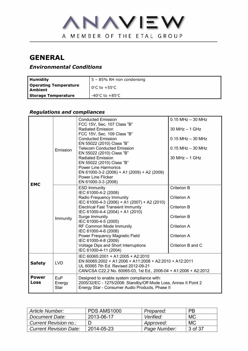
GENERAL Environmental Conditions Humidity 5 – 85% RH non condensing Operating Temperature Ambient 0°C to +55°C
Storage Temperature -40°C to +85°C
Regulations and compliances
EMC
Emission
Conducted Emission FCC 15V, Sec. 107 Class ”B” Radiated Emission FCC 15V, Sec. 109 Class ”B” Conducted Emission EN 55022 (2010) Class ”B” Telecom Conducted Emission EN 55022 (2010) Class ”B” Radiated Emission EN 55022 (2010) Class ”B” Power Line Harmonics EN 61000-3-2 (2006) + A1 (2009) + A2 (2009) Power Line Flicker EN 61000-3-3 (2008)
0.15 MHz – 30 MHz 30 MHz – 1 GHz 0.15 MHz – 30 MHz 0.15 MHz – 30 MHz 30 MHz – 1 GHz
Immunity
ESD Immunity IEC 61000-4-2 (2008) Radio Frequency Immunity IEC 61000-4-3 (2006) + A1 (2007) + A2 (2010) Electrical Fast Transient Immunity IEC 61000-4-4 (2004) + A1 (2010) Surge Immunity IEC 61000-4-5 (2005) RF Common Mode Immunity IEC 61000-4-6 (2008) Power Frequency Magnetic Field IEC 61000-4-8 (2009) Voltage Dips and Short Interruptions IEC 61000-4-11 (2004)
Criterion B Criterion A Criterion B Criterion B Criterion A Criterion A Criterion B and C
Safety LVD IEC 60065:2001 + A1:2005 + A2:2010 EN 60065:2002 + A1:2006 + A11:2008 + A2:2010 + A12:2011 UL 60065 7th Ed. Revised 2012-09-21 CAN/CSA C22.2 No. 60065-03, 1st Ed., 2006-04 + A1:2006 + A2:2012
Power Loss
EuP Energy Star
Designed to enable system compliance with: 2005/32/EC - 1275/2008: Standby/Off Mode Loss, Annex II Point 2 Energy Star - Consumer Audio Products, Phase II

Article Number: PDS AMS1000 Prepared: PB Document Date: 2013-06-17 Verified: MC Current Revision no.: D Approved: MC Current Revision Date: 2014-05-23 Page Number: 4 of 37
Miscellaneous Specifications
Model selection chart/ordering information
Model Accepts Hanger Module†
Application
AMS0100-2600
ü
Auto ranging 2-channel amplifier with 5.5V nominal standby supply meeting Energy Star/EuP and ability to power 3rd channel for 2.1 systems and BTL + SE systems ideal for 2-way LF/HF active speakers.
† Hanger Module Option – offers AUX VS+ and VS- high voltage rails to power an optional Hanger Module amplifier channel.
Cooling Convection cooling
Mounting of the unit See Figure 1 Board outline, dimensions and mounting holes (page 21).
IEC Protection Class Class I Efficiency 85% at 230Vac, 1KHz 1x1000W into 4Ω BTL Idle power consumption < 17.5W at 230VAC Standby mode power consumption 0.5W typically when remote shut down by DISABLE input.
Manufacturing according to workmanship standard IPC-A-610, Revision D, February 2005
Article Number: PDS AMS1000 Prepared: PB Document Date: 2013-06-17 Verified: MC Current Revision no.: D Approved: MC Current Revision Date: 2014-05-23 Page Number: 5 of 37
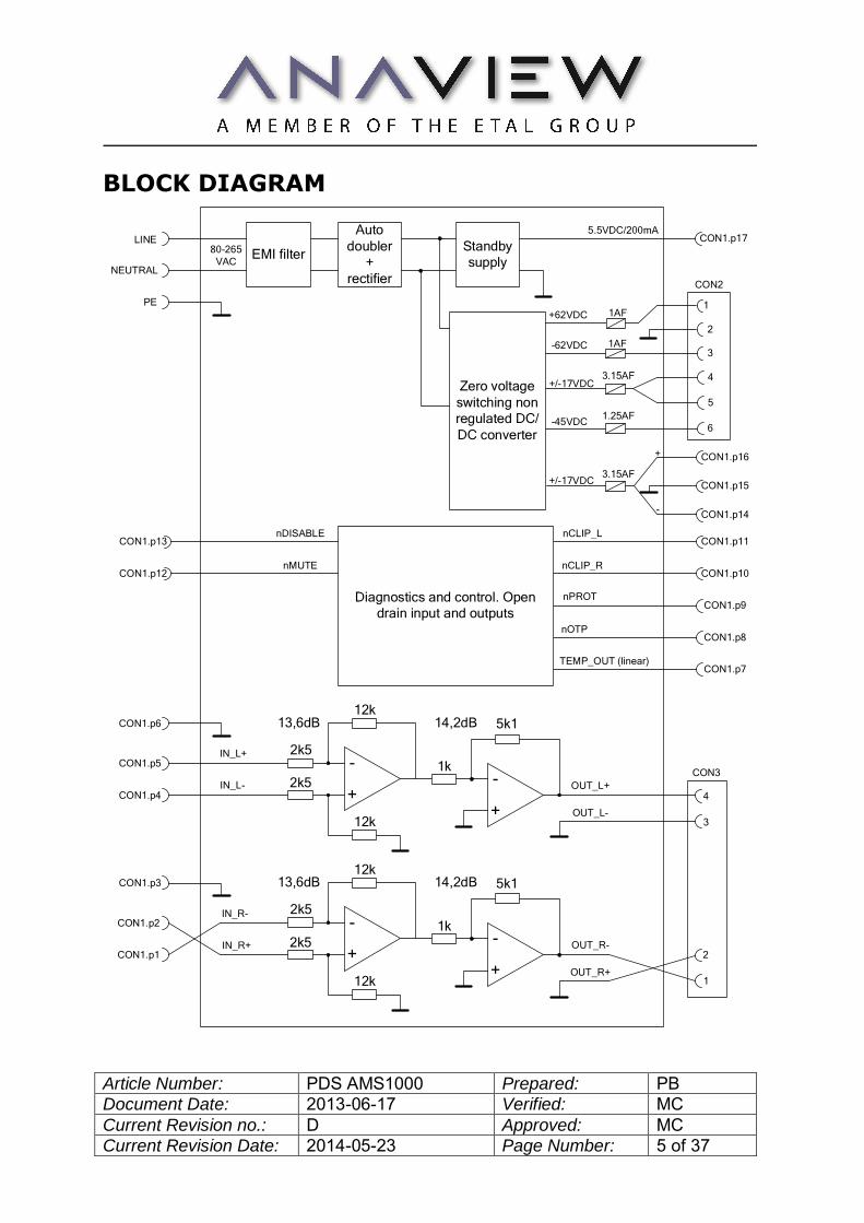
BLOCK DIAGRAM
EMI filter
Auto doubler
+ rectifier
Zero voltage switching non regulated DC/DC converter
Standby supply
5.5VDC/200mACON1.p17
1
3
+62VDC
-62VDC
1AF
1AF2
CON2
80-265VAC
LINE
CON1.p16
CON1.p14
3.15AF+/-17VDC
CON1.p11
CON1.p10
CON1.p9
CON1.p8
CON1.p7
Diagnostics and control. Open drain input and outputs
CON1.p13
CON1.p12
nDISABLE
nMUTE
nCLIP_L
nCLIP_R
nPROT
nOTP
TEMP_OUT (linear)
CON1.p15
+
-
+
-
+
-
2k5
2k5
12k
12k
13,6dB 14,2dB 5k1
1k
+
-
+
-
2k5
2k5
12k
12k
13,6dB 14,2dB 5k1
1k
4
CON3
3
2
1
IN_L+
IN_R-
IN_L-
IN_R+
CON1.p5
CON1.p4
CON1.p2
CON1.p1
CON1.p6
CON1.p3
OUT_L+
OUT_L-
OUT_R-
OUT_R+
4
5
6
+/-17VDC
-45VDC
3.15AF
NEUTRAL
PE
1.25AF
Article Number: PDS AMS1000 Prepared: PB Document Date: 2013-06-17 Verified: MC Current Revision no.: D Approved: MC Current Revision Date: 2014-05-23 Page Number: 6 of 37
MAINS VOLTAGE Absolute maximum ratings
Parameter Comment Min Max Unit Mains input voltage
The module automatically selects between 115/230V operation
75
264 VAC
Mains input freq. 45 63 Hz
Electrical specifications Parameter Comment Min Max Unit
Recommended mains voltage range
For normal operation 90 240 VAC
Minimum mains starting voltage
Where all AUX supplies are available and amplifier is running.
90
VAC
AUDIO SPECIFICATIONS Absolute maximum ratings
Parameter Comment Min Max Unit Input signal single ended
Between IN_L+ and GND Between IN_L- and GND Between IN_R+ and GND Between IN_R- and GND
- 3 Vrms
Input signal balanced
Between IN_L+ and IN_L- Between IN_R+ and IN_R-
- 6 Vrms
Electrical specifications Measured at 25°C ambient with no preheating unless otherwise specified
Parameter Comment Min Typ Max Unit Offset voltage With open inputs 10 mV Switching frequency At idle with 4Ω load 370 kHz Switching residual At idle with 4Ω load 800 mVpk Gain At 1kHz with 4Ω load 27,5 dB Idle noise Unweighted with 4Ω load 60 µVrms SNR 1W 4Ω 2.81Vrms/idle noise 93 dB SNR 1W 2Ω 2.0Vrms/idle noise 90 dB Dynamic range 4Ω 36Vrms/idle noise 115 dB Common mode rejection
IN+ and IN- connected together. 100Hz signal applied to input. Rejection measured at the output.
38 dB

Article Number: PDS AMS1000 Prepared: PB Document Date: 2013-06-17 Verified: MC Current Revision no.: D Approved: MC Current Revision Date: 2014-05-23 Page Number: 7 of 37
Input impedance single ended (*1)
Non symmetrical on positive and negative inputs
2.5 14.5 kΩ
Input impedance balanced (*1)
Non symmetrical on positive and negative inputs
1.37 14.5 kΩ
Upper bandwidth limit
Point of -3dB vs gain at 1kHz with 4Ω load
70 kHz
Gain deviation From 20Hz to 20kHz 0.5 dB Upper full power bandwidth (*2)
Level calibrated at 1% THD at 1kHz.
20 kHz
Lower bandwidth limit (*3)
Point of -3dB vs gain at 1kHz with 4Ω load
4 Hz
Recommended load impedance single ended
Recommended for optimized efficiency and audio performance
2 8 Ω
Recommended load impedance BTL
Recommended for optimized efficiency and audio performance
4 8 Ω
Output impedance @ 100Hz
Measuring output voltage while injecting 1Arms into output. 1mV=1mΩ
6 mΩ
Output impedance @ 20kHz
Measuring output voltage while injecting 1Arms into output. 1mV=1mΩ
13 mΩ
(*1) The input impedance on IN+ and IN- is not identical and also different between channels. See application notes below for more information.
(*2) Sustained operation at full power above this frequency may result in damage to the module. (*3) Requires symmetrical loading and signal generation on both channels.
Power specifications SE operation Maximum output current
Measured with one period of 100Hz sine wave
30 Apk
Maximum long term output power into 8Ω
Measured with both channels driven @ 1% THD+N
2x170 Wrms
Maximum long term output power into 4Ω
Measured with both channels driven @ 1% THD+N
2x300 Wrms
Maximum long term output power into 2Ω
Measured with both channels driven @ 1% THD+N
2x500 Wrms
Maximum infinite output power into 4Ω
Measured with both channels driven in 45°C ambient temperature.
2x100 Wrms
Maximum infinite output power into 2Ω
Measured with both channels driven in 45°C ambient temperature.
2x75 Wrms
FTC power rating into 8Ω
1 hour pre heating with 1/8 of specified power and subsequently 5 min. with specified power at 120/230Vac, 1kHz input, ambient
2x170 Wrms

Article Number: PDS AMS1000 Prepared: PB Document Date: 2013-06-17 Verified: MC Current Revision no.: D Approved: MC Current Revision Date: 2014-05-23 Page Number: 8 of 37
temp. 25°C still air. Open frame. Board mounted vertically.
FTC power rating into 4Ω
1 hour pre heating with 1/8 of specified power and subsequently 5 min. with specified power at 120/230Vac, 1kHz input, ambient temp. 25°C still air. Open frame. Board mounted vertically.
2x300 Wrms
FTC power rating into 2Ω
1 hour pre heating with 1/8 of specified power and subsequently 5 min. with specified power at 120/230Vac, 1kHz input, ambient temp. 25°C still air. Open frame. Board mounted vertically.
2x250 Wrms
Max short term RMS power into 8Ω
500ms of 1kHz sine wave @ 1%THD. One channel.
180 Wrms
Max short term RMS power into 4Ω
500ms of 1kHz sine wave @ 1%THD. One channel.
360 Wrms
Max short term RMS power into 2Ω
500ms of 1kHz sine wave @ 1%THD. One channel.
680 Wrms
Power specifications BTL operation Maximum long term output power into 8Ω
Measured during 30 second interval with 1% THD+N
580 Wrms
Maximum long term output power into 6Ω
Measured during a 30 second interval with 1% THD+N
720 Wrms
Maximum long term output power into 4Ω
Measured during a 30 second interval with 1% THD+N
900 Wrms
Maximum continuous output power into 8Ω
Measured in 45°C ambient temperature.
200 Wrms
Maximum continuous output power into 6Ω
Measured in 45°C ambient temperature.
170 Wrms
Maximum continuous output power into 4Ω
Measured in 45°C ambient temperature.
150 Wrms
FTC power rating into 8Ω
1 hour pre heating with 1/8 of specified power and subsequently 5 min. with specified power at 120/230Vac, 1kHz input, ambient temp. 25°C still air. Open frame. Board mounted vertically.
570 Wrms
FTC power rating into 6Ω
1 hour pre heating with 1/8 of specified power and subsequently 5 min. with specified power at 120/230Vac, 1kHz input, ambient temp. 25°C still air. Open frame. Board mounted vertically.
600 Wrms
FTC power rating into 4Ω
1 hour pre heating with 1/8 of specified power and subsequently 5 min. with specified power at 120/230Vac, 1kHz input, ambient temp. 25°C still air. Open frame.
500 Wrms

Article Number: PDS AMS1000 Prepared: PB Document Date: 2013-06-17 Verified: MC Current Revision no.: D Approved: MC Current Revision Date: 2014-05-23 Page Number: 9 of 37
Board mounted vertically. Max short term RMS power into 8Ω
500ms of 1kHz sine wave @ 1%THD.
590 Wrms
Max short term RMS power into 6Ω
500ms of 1kHz sine wave @ 1%THD.
740 Wrms
Max short term RMS power into 4Ω
500ms of 1kHz sine wave @ 1%THD.
1000 Wrms

Article Number: PDS AMS1000 Prepared: PB Document Date: 2013-06-17 Verified: MC Current Revision no.: D Approved: MC Current Revision Date: 2014-05-23 Page Number: 10 of 37
DIAGNOSTIC SIGNALS Diagnostics outputs Output type
Voltage range I Max cont. Function
Min Max
nPROT Open drain
with 2kohm in series(*1)
N/A VA+(*3) 5mA
Signals during: - Over voltage shutdown
- VA+/- fuse is blown - Startup until rails are OK
nCLIP_L Open drain
with 2kohm in series(*1)
N/A VA+(*3) 5mA Signals when the output generates >0,1%THD+N
nCLIP_R Open drain
with 2kohm in series(*1)
N/A VA+(*3) 5mA Signals when the output generates >0,1%THD+N
nOTP Open drain
with 2kohm in series(*1)
N/A VA+(*3) 5mA Signals when the hottest
component reaches approx 110°C
TEMP_OUT Linear(*2) 0.2V 3.0V 5mA
Displays the temperature of the hottest component
inside AMS1000. Shut down is 2.86V.
(*1) Open drain outputs with 2kohm in series to limit the current.
(*2) The TEMP_OUT output is a linear signal with 1kohm in series to limit the current. (*3) Recommended maximum voltage to which a pull up resistor should be connected.

Article Number: PDS AMS1000 Prepared: PB Document Date: 2013-06-17 Verified: MC Current Revision no.: D Approved: MC Current Revision Date: 2014-05-23 Page Number: 11 of 37
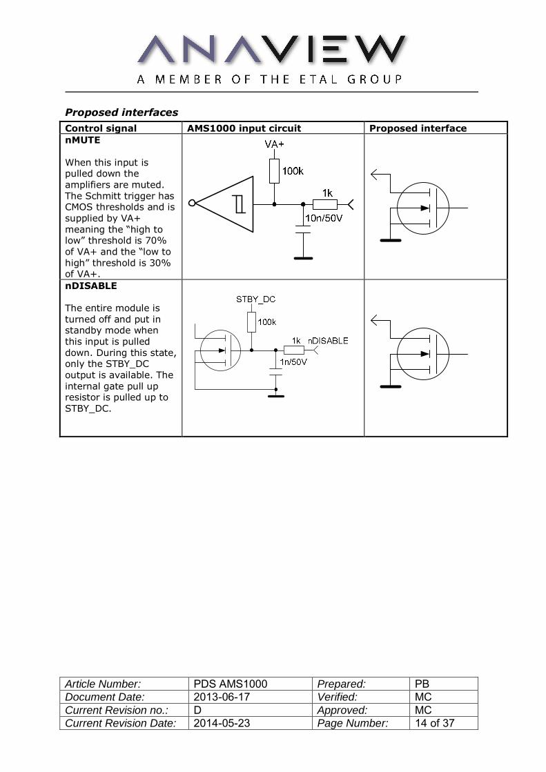
Proposed interfaces Diagnostics output AMS1000 output circuit Proposed interface nPROT, nCLIP_L, nCLIP_R, nOTP. The MOSFET 2N7002 is turned on during the corresponding situations.
TEMP_OUT This output shows the temperature of the hottest position inside the module. Internal supervision shuts down the amplifiers when this output reaches 2,87V which corresponds to 100°C.

Article Number: PDS AMS1000 Prepared: PB Document Date: 2013-06-17 Verified: MC Current Revision no.: D Approved: MC Current Revision Date: 2014-05-23 Page Number: 12 of 37
Temp out The below graph shows how the output signal TEMP_OUT follows the hottest component in the AMS1000 module. X-axis is voltage and Y-axis is temperature in °C. 2.86V on TEMP_OUT signal is shut down threshold.
The temperature can also be described using the formula below
TEMP=(3428/LN(53532-(15851*TEMP_OUT)))-273,15
40
50
60
70
80
90
100
110
120
130
140
0,9 1 1,1 1,2 1,3 1,4 1,5 1,6 1,7 1,8 1,9 2 2,1 2,2 2,3 2,4 2,5 2,6 2,7 2,8 2,9 3 3,1 3,2

Article Number: PDS AMS1000 Prepared: PB Document Date: 2013-06-17 Verified: MC Current Revision no.: D Approved: MC Current Revision Date: 2014-05-23 Page Number: 13 of 37
CONTROL INPUTS Absolute maximum ratings
Parameter Comment Min Max Unit nDISABLE 0 VA+ V nMUTE 0 VA+ V
Electrical specifications Parameter Comment Min Typ Max Unit
nDISABLE activation threshold
Threshold for disabling the AMS1000 module (active low)
1.0 2.0 2.75 V
nDISABLE deactivation threshold
Threshold for enabling the AMS1000 module
1.0
2.0 2.75 V
nDISABLE activation time
Time from setting nDISABLE low to amplifier stop
0.7 ms
nDISABLE deactivation time
Time from setting nDISABLE high to amplifier start
1500 ms
nMUTE activation threshold
Threshold for muting the AMS1000 module (active low). 30% of VA+.
0.3xVa+ V
nMUTE deactivation threshold
Threshold for unmuting the AMS1000 module. 70% of VA+.
0.7xVa+ V
nMUTE activation time
Time from setting nMUTE low to amplifier stop
1 ms
nMUTE deactivation time
Time from setting nMUTE high to amplifier start
8 ms
Article Number: PDS AMS1000 Prepared: PB Document Date: 2013-06-17 Verified: MC Current Revision no.: D Approved: MC Current Revision Date: 2014-05-23 Page Number: 14 of 37
Proposed interfaces Control signal AMS1000 input circuit Proposed interface nMUTE When this input is pulled down the amplifiers are muted. The Schmitt trigger has CMOS thresholds and is supplied by VA+ meaning the “high to low” threshold is 70% of VA+ and the “low to high” threshold is 30% of VA+.
nDISABLE The entire module is turned off and put in standby mode when this input is pulled down. During this state, only the STBY_DC output is available. The internal gate pull up resistor is pulled up to STBY_DC.
Article Number: PDS AMS1000 Prepared: PB Document Date: 2013-06-17 Verified: MC Current Revision no.: D Approved: MC Current Revision Date: 2014-05-23 Page Number: 15 of 37
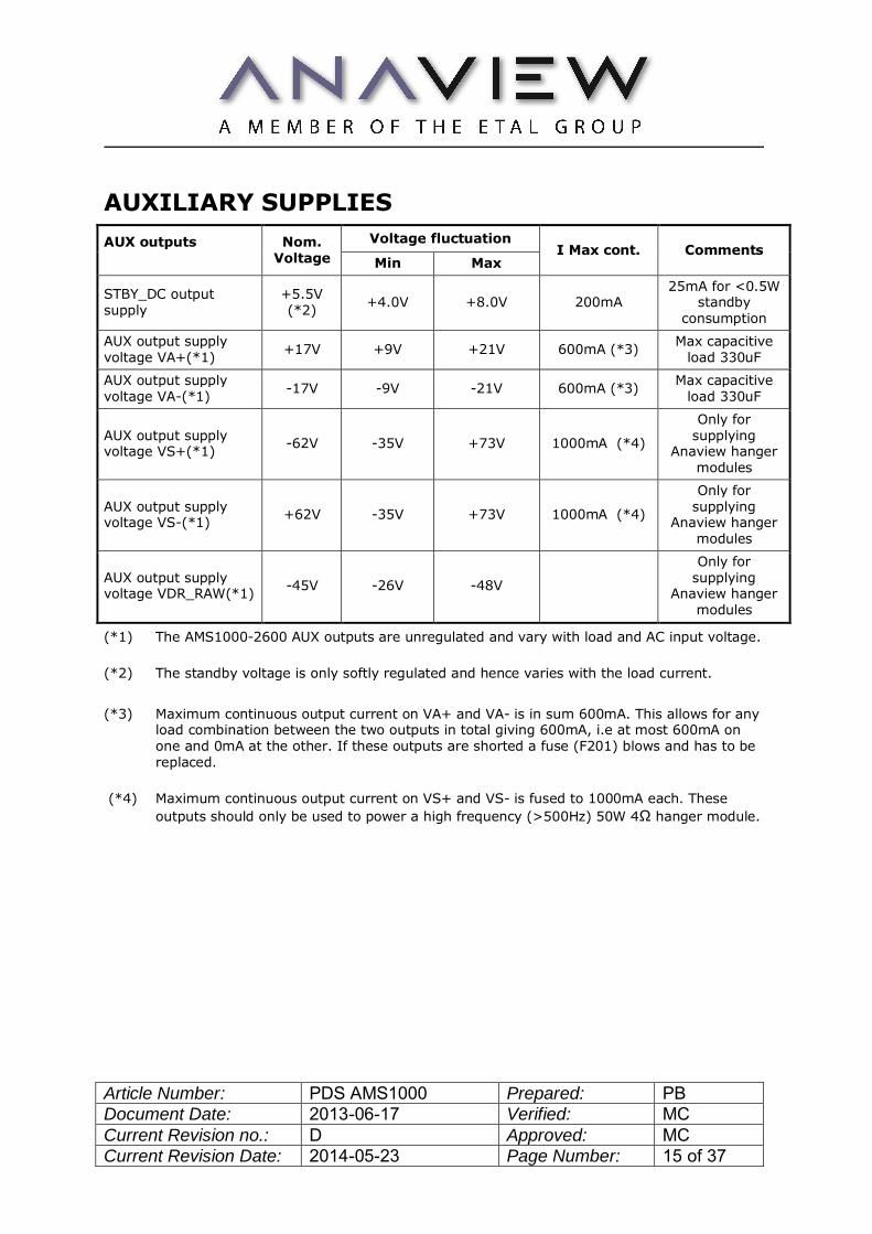
AUXILIARY SUPPLIES AUX outputs
Nom. Voltage
Voltage fluctuation I Max cont. Comments
Min Max
STBY_DC output supply
+5.5V (*2) +4.0V +8.0V 200mA
25mA for <0.5W standby
consumption
AUX output supply voltage VA+(*1) +17V +9V +21V 600mA (*3) Max capacitive
load 330uF
AUX output supply voltage VA-(*1) -17V -9V -21V 600mA (*3) Max capacitive
load 330uF
AUX output supply voltage VS+(*1) -62V -35V +73V 1000mA (*4)
Only for supplying
Anaview hanger modules
AUX output supply voltage VS-(*1) +62V -35V +73V 1000mA (*4)
Only for supplying
Anaview hanger modules
AUX output supply voltage VDR_RAW(*1) -45V -26V -48V
Only for supplying
Anaview hanger modules
(*1) The AMS1000-2600 AUX outputs are unregulated and vary with load and AC input voltage. (*2) The standby voltage is only softly regulated and hence varies with the load current. (*3) Maximum continuous output current on VA+ and VA- is in sum 600mA. This allows for any
load combination between the two outputs in total giving 600mA, i.e at most 600mA on one and 0mA at the other. If these outputs are shorted a fuse (F201) blows and has to be replaced.
(*4) Maximum continuous output current on VS+ and VS- is fused to 1000mA each. These
outputs should only be used to power a high frequency (>500Hz) 50W 4Ω hanger module.
Article Number: PDS AMS1000 Prepared: PB Document Date: 2013-06-17 Verified: MC Current Revision no.: D Approved: MC Current Revision Date: 2014-05-23 Page Number: 16 of 37
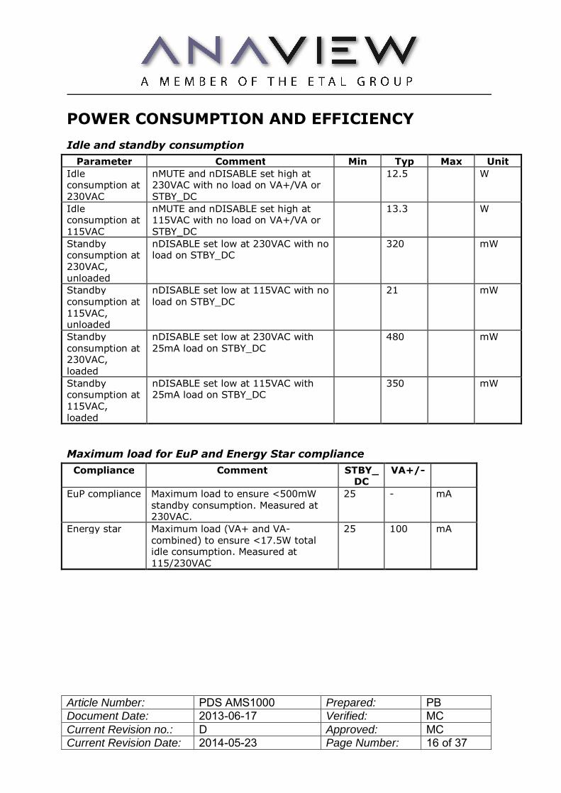
POWER CONSUMPTION AND EFFICIENCY Idle and standby consumption
Parameter Comment Min Typ Max Unit Idle consumption at 230VAC
nMUTE and nDISABLE set high at 230VAC with no load on VA+/VA or STBY_DC
12.5 W
Idle consumption at 115VAC
nMUTE and nDISABLE set high at 115VAC with no load on VA+/VA or STBY_DC
13.3 W
Standby consumption at 230VAC, unloaded
nDISABLE set low at 230VAC with no load on STBY_DC
320 mW
Standby consumption at 115VAC, unloaded
nDISABLE set low at 115VAC with no load on STBY_DC
21 mW
Standby consumption at 230VAC, loaded
nDISABLE set low at 230VAC with 25mA load on STBY_DC
480 mW
Standby consumption at 115VAC, loaded
nDISABLE set low at 115VAC with 25mA load on STBY_DC
350 mW
Maximum load for EuP and Energy Star compliance Compliance Comment STBY_
DC VA+/-
EuP compliance Maximum load to ensure <500mW standby consumption. Measured at 230VAC.
25 - mA
Energy star Maximum load (VA+ and VA- combined) to ensure <17.5W total idle consumption. Measured at 115/230VAC
25 100 mA
Article Number: PDS AMS1000 Prepared: PB Document Date: 2013-06-17 Verified: MC Current Revision no.: D Approved: MC Current Revision Date: 2014-05-23 Page Number: 17 of 37
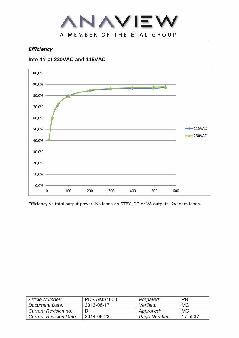
Efficiency
Into 4Ω at 230VAC and 115VAC
Efficiency vs total output power. No loads on STBY_DC or VA outputs. 2x4ohm loads.
0,0%
10,0%
20,0%
30,0%
40,0%
50,0%
60,0%
70,0%
80,0%
90,0%
100,0%
0 100 200 300 400 500 600
115VAC
230VAC
Article Number: PDS AMS1000 Prepared: PB Document Date: 2013-06-17 Verified: MC Current Revision no.: D Approved: MC Current Revision Date: 2014-05-23 Page Number: 18 of 37
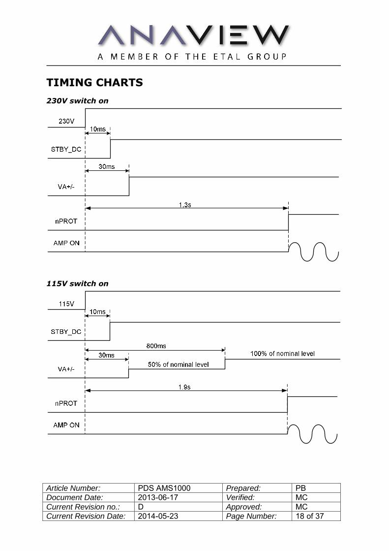
TIMING CHARTS 230V switch on
115V switch on
Article Number: PDS AMS1000 Prepared: PB Document Date: 2013-06-17 Verified: MC Current Revision no.: D Approved: MC Current Revision Date: 2014-05-23 Page Number: 19 of 37
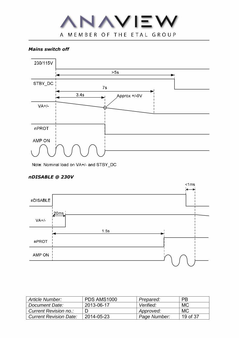
Mains switch off
nDISABLE @ 230V
Article Number: PDS AMS1000 Prepared: PB Document Date: 2013-06-17 Verified: MC Current Revision no.: D Approved: MC Current Revision Date: 2014-05-23 Page Number: 20 of 37
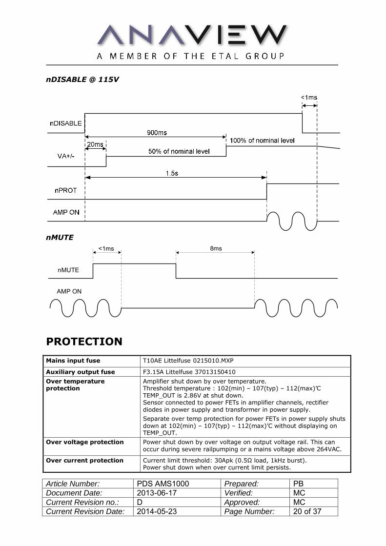
nDISABLE @ 115V
nMUTE
nMUTE
AMP ON
<1ms 8ms
PROTECTION Mains input fuse T10AE Littelfuse 0215010.MXP
Auxiliary output fuse F3.15A Littelfuse 37013150410 Over temperature protection
Amplifier shut down by over temperature. Threshold temperature : 102(min) – 107(typ) – 112(max)’C TEMP_OUT is 2.86V at shut down. Sensor connected to power FETs in amplifier channels, rectifier diodes in power supply and transformer in power supply. Separate over temp protection for power FETs in power supply shuts down at 102(min) – 107(typ) – 112(max)’C without displaying on TEMP_OUT.
Over voltage protection Power shut down by over voltage on output voltage rail. This can occur during severe railpumping or a mains voltage above 264VAC.
Over current protection Current limit threshold: 30Apk (0.5Ω load, 1kHz burst). Power shut down when over current limit persists.

Article Number: PDS AMS1000 Prepared: PB Document Date: 2013-06-17 Verified: MC Current Revision no.: D Approved: MC Current Revision Date: 2014-05-23 Page Number: 21 of 37
CONNECTIONS Connector Connector type Mating connector CON1 (signal) 17 pin JST B17B-CZHK-B-1 JST 17CZ-6H
Crimp terminal SCZH-002T-P0.5 CON2 (Vs/Va) 6 pin CVIlux CP3506P1V00 CVIlux CP3506S0010
Crimp terminal CVIlux CP35TN21PES CON3 (speakers) 4 pin JST B04P-VL JST VLP-04V
Crimp terminal BVF-61T-P2.0 LINE PCB terminal 4.8x0.8mm NEUTRAL PCB terminal 4.8x0.8mm PE PCB terminal 4.8x0.8mm
Signal connector pinning (CON1) 1 IN_R- Right audio channel negative input. 2 IN_R+ Right audio channel positive input. 3 GNDs Secondary side ground 4 IN_L- Left audio channel negative input. 5 IN_L+ Left audio channel positive input. 6 GNDs Secondary side ground 7 TEMP_OUT Linear temp output signal. 8 nOTP Over temp shutdown output signal. 9 nPROT PSU shutdown output signal. 10 nCLIP_R Clip detect output signal. 11 nCLIP_L Clip detect output signal. 12 nMUTE Mute input signal. 13 nDISABLE Standby mode activation signal. 14 VA- AUX output voltage VA- 15 GNDs Secondary side ground 16 VA+ AUX output voltage VA+ 17 STBY_DC AUX output voltage STBY_DC
Signal connector pinning (CON2) 1 VS+ VS+ with 1A fuse 2 GND Secondary side ground 3 VS- VS- with 1A fuse 4 VA+ VA+ 5 VA- VA- 6 VDR_RAW Gate voltage referred to VS-
Article Number: PDS AMS1000 Prepared: PB Document Date: 2013-06-17 Verified: MC Current Revision no.: D Approved: MC Current Revision Date: 2014-05-23 Page Number: 22 of 37
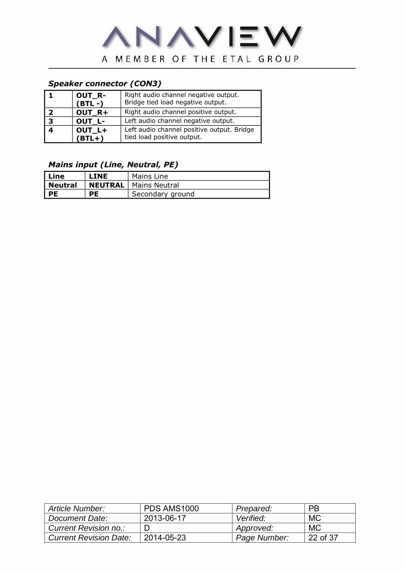
Speaker connector (CON3) 1 OUT_R-
(BTL -) Right audio channel negative output. Bridge tied load negative output.
2 OUT_R+ Right audio channel positive output. 3 OUT_L- Left audio channel negative output. 4 OUT_L+
(BTL+) Left audio channel positive output. Bridge tied load positive output.
Mains input (Line, Neutral, PE) Line LINE Mains Line Neutral NEUTRAL Mains Neutral PE PE Secondary ground
Article Number: PDS AMS1000 Prepared: PB Document Date: 2013-06-17 Verified: MC Current Revision no.: D Approved: MC Current Revision Date: 2014-05-23 Page Number: 23 of 37
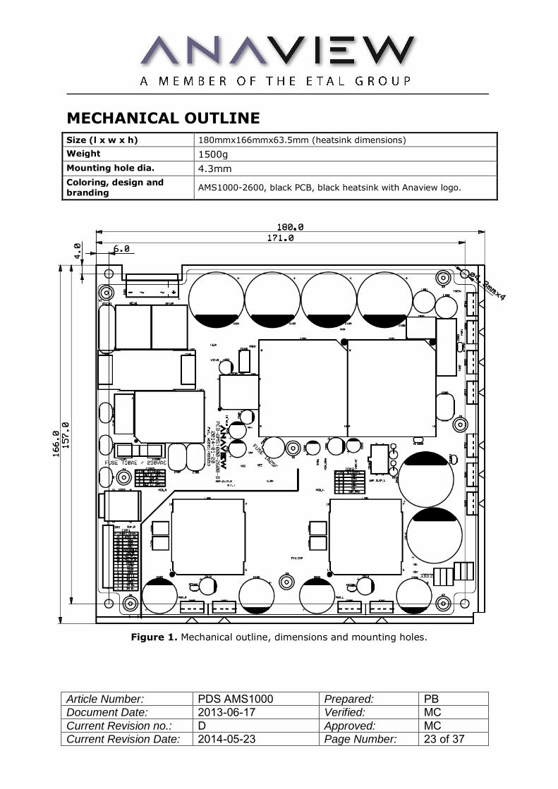
MECHANICAL OUTLINE Size (l x w x h) 180mmx166mmx63.5mm (heatsink dimensions) Weight 1500g Mounting hole dia. 4.3mm Coloring, design and branding AMS1000-2600, black PCB, black heatsink with Anaview logo.
Figure 1. Mechanical outline, dimensions and mounting holes.

Article Number: PDS AMS1000 Prepared: PB Document Date: 2013-06-17 Verified: MC Current Revision no.: D Approved: MC Current Revision Date: 2014-05-23 Page Number: 24 of 37
AUDIO MEASUREMENTS
Figure 2. Frequency response 4Ω, 8Ω and open load SE.
Figure 3. Phase response 4Ω, 8Ω and open load SE.
Article Number: PDS AMS1000 Prepared: PB Document Date: 2013-06-17 Verified: MC Current Revision no.: D Approved: MC Current Revision Date: 2014-05-23 Page Number: 25 of 37
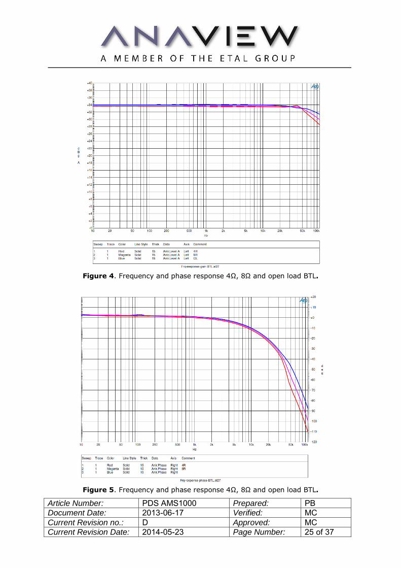
Figure 4. Frequency and phase response 4Ω, 8Ω and open load BTL.
Figure 5. Frequency and phase response 4Ω, 8Ω and open load BTL.
Article Number: PDS AMS1000 Prepared: PB Document Date: 2013-06-17 Verified: MC Current Revision no.: D Approved: MC Current Revision Date: 2014-05-23 Page Number: 26 of 37
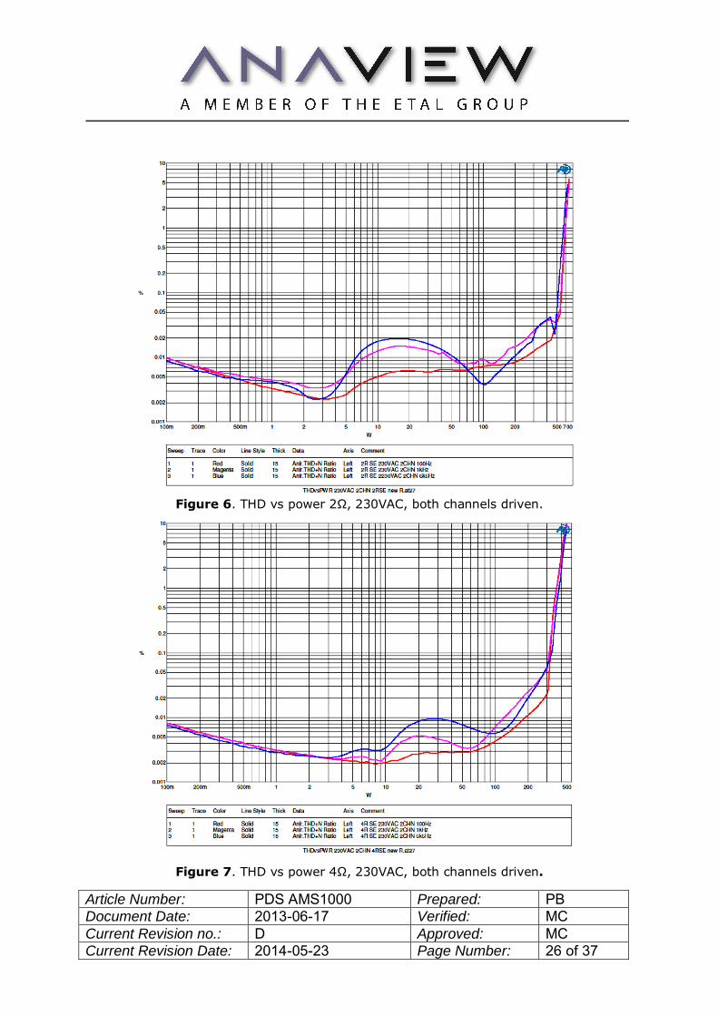
Figure 6. THD vs power 2Ω, 230VAC, both channels driven.
Figure 7. THD vs power 4Ω, 230VAC, both channels driven.

Article Number: PDS AMS1000 Prepared: PB Document Date: 2013-06-17 Verified: MC Current Revision no.: D Approved: MC Current Revision Date: 2014-05-23 Page Number: 27 of 37
Figure 8. THD vs power, 2Ω, 115VAC, both channels driven.
Figure 9. THD vs power, 6Ω, 115VAC, both channels driven.
Article Number: PDS AMS1000 Prepared: PB Document Date: 2013-06-17 Verified: MC Current Revision no.: D Approved: MC Current Revision Date: 2014-05-23 Page Number: 28 of 37
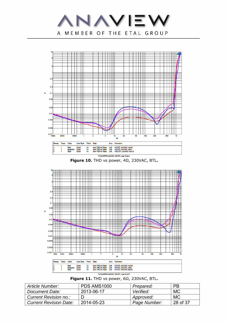
Figure 10. THD vs power, 4Ω, 230VAC, BTL.
Figure 11. THD vs power, 6Ω, 230VAC, BTL.

Article Number: PDS AMS1000 Prepared: PB Document Date: 2013-06-17 Verified: MC Current Revision no.: D Approved: MC Current Revision Date: 2014-05-23 Page Number: 29 of 37
Figure 12. THD vs power, 8Ω BTL, 230VAC.
Figure 13. Output impedance 1mV=1mΩ.

Article Number: PDS AMS1000 Prepared: PB Document Date: 2013-06-17 Verified: MC Current Revision no.: D Approved: MC Current Revision Date: 2014-05-23 Page Number: 30 of 37
Figure 14. Crosstalk.
Figure 13. THD vs frequency

Article Number: PDS AMS1000 Prepared: PB Document Date: 2013-06-17 Verified: MC Current Revision no.: D Approved: MC Current Revision Date: 2014-05-23 Page Number: 31 of 37
INSTRUCTIONS Replacing VA+/VA- fuse The auxiliary supplies VA+/- are protected by a fuse. In case of overload this fuse will open and has to be replaced to get the supplies back.
F201 is a 3.15A fast acting fuse from Littelfuse with article number 37013150410. The maximum load on VA+/- can be seen in the table on page 15. The fuse value of F3.15A was choosen to tolerate the start-up charge energy of a capacitive load.
Article Number: PDS AMS1000 Prepared: PB Document Date: 2013-06-17 Verified: MC Current Revision no.: D Approved: MC Current Revision Date: 2014-05-23 Page Number: 32 of 37
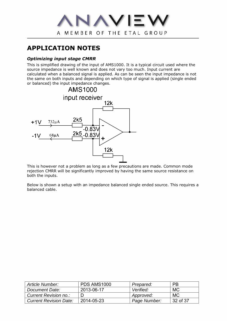
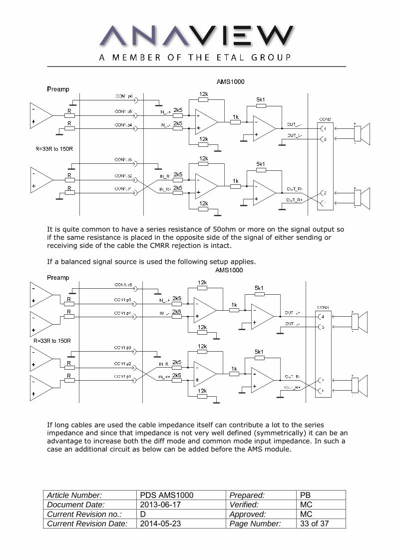
APPLICATION NOTES Optimizing input stage CMRR This is simplified drawing of the input of AMS1000. It is a typical circuit used where the source impedance is well known and does not vary too much. Input current are calculated when a balanced signal is applied. As can be seen the input impedance is not the same on both inputs and depending on which type of signal is applied (single ended or balanced) the input impedance changes.
This is however not a problem as long as a few precautions are made. Common mode rejection CMRR will be significantly improved by having the same source resistance on both the inputs. Below is shown a setup with an impedance balanced single ended source. This requires a balanced cable.
Article Number: PDS AMS1000 Prepared: PB Document Date: 2013-06-17 Verified: MC Current Revision no.: D Approved: MC Current Revision Date: 2014-05-23 Page Number: 33 of 37
It is quite common to have a series resistance of 50ohm or more on the signal output so if the same resistance is placed in the opposite side of the signal of either sending or receiving side of the cable the CMRR rejection is intact. If a balanced signal source is used the following setup applies.
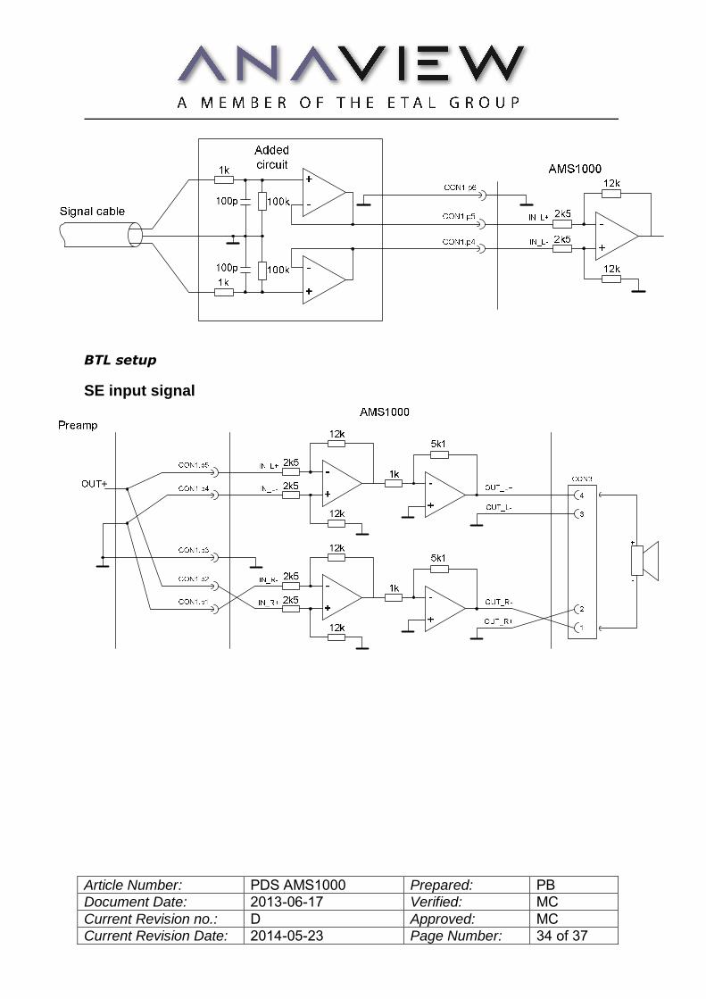
If long cables are used the cable impedance itself can contribute a lot to the series impedance and since that impedance is not very well defined (symmetrically) it can be an advantage to increase both the diff mode and common mode input impedance. In such a case an additional circuit as below can be added before the AMS module.
Article Number: PDS AMS1000 Prepared: PB Document Date: 2013-06-17 Verified: MC Current Revision no.: D Approved: MC Current Revision Date: 2014-05-23 Page Number: 34 of 37
BTL setup
SE input signal
Article Number: PDS AMS1000 Prepared: PB Document Date: 2013-06-17 Verified: MC Current Revision no.: D Approved: MC Current Revision Date: 2014-05-23 Page Number: 35 of 37
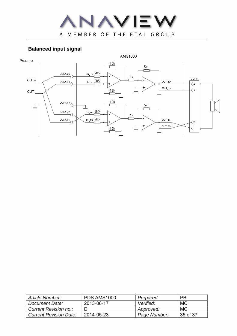
Balanced input signal
Article Number: PDS AMS1000 Prepared: PB Document Date: 2013-06-17 Verified: MC Current Revision no.: D Approved: MC Current Revision Date: 2014-05-23 Page Number: 36 of 37
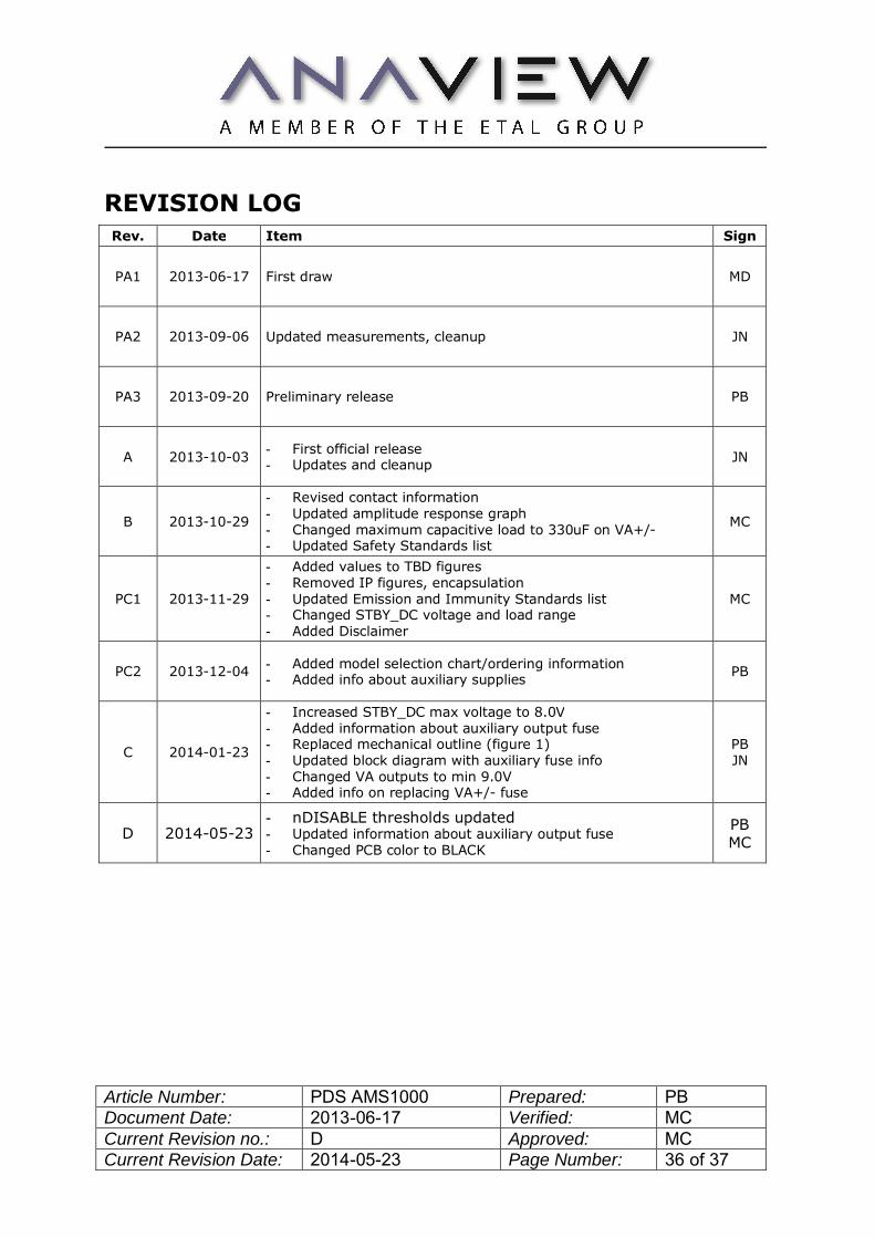
REVISION LOG Rev. Date Item Sign
PA1 2013-06-17 First draw MD
PA2 2013-09-06 Updated measurements, cleanup JN
PA3 2013-09-20 Preliminary release PB
A 2013-10-03 - First official release - Updates and cleanup JN
B 2013-10-29
- Revised contact information - Updated amplitude response graph - Changed maximum capacitive load to 330uF on VA+/- - Updated Safety Standards list
MC
PC1 2013-11-29
- Added values to TBD figures - Removed IP figures, encapsulation - Updated Emission and Immunity Standards list - Changed STBY_DC voltage and load range - Added Disclaimer
MC
PC2 2013-12-04 - Added model selection chart/ordering information - Added info about auxiliary supplies PB
C 2014-01-23
- Increased STBY_DC max voltage to 8.0V - Added information about auxiliary output fuse - Replaced mechanical outline (figure 1) - Updated block diagram with auxiliary fuse info - Changed VA outputs to min 9.0V - Added info on replacing VA+/- fuse
PB JN
D 2014-05-23 - nDISABLE thresholds updated - Updated information about auxiliary output fuse - Changed PCB color to BLACK
PB MC

Article Number: PDS AMS1000 Prepared: PB Document Date: 2013-06-17 Verified: MC Current Revision no.: D Approved: MC Current Revision Date: 2014-05-23 Page Number: 37 of 37
ANAVIEW CONTACT INFORMATION For further information about Anaview’s products and technology please contact: Email: [email protected] Website: www.anaview.com Anaview (Europe, APAC) Södergatan 4 25225 Helsingborg Sweden
Anaview (North America) PO Box 459 Manasquan, NJ 08736 New Jersey USA
Part of ETAL Group AB Fagerstagatan 3 SE-163 53 SPÅNGA SWEDEN