Product Portfolio Inrevium - Fujitsu Global · Inrevium Product Portfolio ... o SPI Flash 128Mbit...
17
0 | Page 2017 PRODUCT PORTFOLIO INREVIUM
Transcript of Product Portfolio Inrevium - Fujitsu Global · Inrevium Product Portfolio ... o SPI Flash 128Mbit...

0 | P a g e
2017
PRODUCT PORTFOLIO INREVIUM

1 | P a g e
Inrevium Product Portfolio
Contents
Contents .................................................................................................................................................. 1
Base Boards ............................................................................................................................................. 2
Virtex UltraScale – High Density Scalable ASIC Prototyping Platform ................................................ 2
Kintex UltraScale – 8K4K Image Evaluation Platform ......................................................................... 3
Kintex UltraScale – ACDC Quattro Kintex UltraScale Development Platform ..................................... 4
Virtex-7 – FPGA ASIC Development Test Platform .............................................................................. 5
Virtex-7 – FPGA Large-Scale PCI Express Gen3 Evaluation Platform .................................................. 6
Kintex-7 – ACDC (Acquisition, Contribution, Distribution Consumption) 1.0 Base board ................... 7
Artix-7 – ACDC A7 Evaluation Board ................................................................................................... 8
Zynq-7000 – All Programmable SoC Extension Microcontroller Card ................................................. 9
Zynq-7000 – Industrial Grade SOM (System on Module) .................................................................. 10
Zynq-7000 – Industrial Grade SOM (System On Module) Development Kit...................................... 11
FPGA Mezzanine Cards (FMC) ............................................................................................................... 12
High Pin Count FMC .......................................................................................................................... 12
Low Pin Count FMC ........................................................................................................................... 13
IP Cores.................................................................................................................................................. 14
V-by-ONE HS IP Core ......................................................................................................................... 14
MECHATROLINK – III Master IP Core ................................................................................................. 14
3D ToF Camera Module ........................................................................................................................ 15

2 | P a g e
Base Boards
Virtex UltraScale – High Density Scalable ASIC Prototyping Platform
The Virtex UltraScale prototyping platform is intended for development of large SoCs and incorporates
single/dual Virtex UltraScale 440 FPGAs, the world’s largest FPGA with performance features that include high‐
speed internal logic and high‐bandwidth interfaces.
FEATURES
Shorten development time by providing an
ASIC emulation platform
2 kinds of memory modules: DDR4 SODIMM
and DDR3 SODIMM.
Support software adjustment for FMC I/O ADJ
voltage.
BLOCK DIAGRAM
Part Number: TBS-VU-440-LSI SOLO/DUAL
DESCRIPTION
Device: o XCVU440-2FLVA2892C x1 (solo) / x2(dual) o XC7Z030-2FFG676 x1
Memory: o Up to 8GB(solo) / 16GB(dual) DDR3 and/or
DDR4 SODIMM
Interface o 4x(solo) / 8x(dual) HPC-FMC connectors o 5x(solo) / 10x (dual) QTH connectors o Total up to 2250 GPIO, 88 GTH o USB 3.0 o Gigabit Ethernet o JTAG header o UART debug pin o PMOD interface o Power LEDs o DIP/Push switches, LEDs, Test pins
Configuration: o microSD Card o SPI Flash

3 | P a g e
Kintex UltraScale – 8K4K Image Evaluation Platform
The platform accelerate development Super-High Definition 8K image Processing
Features 20nm Kintex UltraSCALE XCKU060/115-
2FFVA1517
2xDDR4 SDRAM(2,400Mbps)64bit enables wide band data buffer
Provide the extensibility with GTH transceiver
o 7xFMC connectors (see the example table below)
o On board 4xSFP + socket for Video stream
through Ethernet
Part Number TB-KU-060-ACDC-8K / TB-KU-
115-ACDC-8K
Description Device : XCKU060/115-2FFVA1517
Memory : DDR4-SDRAM (64bit) x2
Interface : o FMC
1
o SFP + Socket o RS-232C (Connector is USB-B type) o PMOD (Digilent module interface) o 10pin header for XILINX cable o General pin header o Push switch , DIP switch , LED
Clock : o 200MHz for DDR4 o 148.5MHz for image processing o 156.25MHz for high speed Serdes o PLL for general purpose
Configuration : QUAD Dual-SPI Flash
Board size:H280 x W313(mm)
Power (AC adopter)
Reference Design
DDR4 memory controller (MIG)
FMC Connection: Chip2Chip design
1 Not all VITA57.1 signals are populated.

4 | P a g e
Kintex UltraScale – ACDC Quattro Kintex UltraScale Development Platform
The Quattro platform accelerates development across a wide range of industries including but not limited to
Video/Broadcast, Aerospace and Communications.
Features 20nm Kintex UltraScale FPGA
2x DDR4 SDRAM (2,400Mbps) 64-bit enables wideband data buffering
Expandable via four (4) FMC HPC connectors o 10 GTH transceivers per FMC (one
implemented as 8+2 due to SLR)
Substantial I/Os for LVDS or single ended connectivity
On board SFP+ socket for Video stream through Ethernet
Part Number TB-KU-115-QUATTRO
Description Device : Kintex UltraScale XCKU115-2FFVA1517
Memory: 4GB DDR4-SDRAM (64bit) 2,400Mbps
Interface : o FMC x4
2
o On board Zynq for system management and processing
o SFP+ Interface o General purpose LEDs and switches o Proven operation with inrevium HDMI4K,
12G-SDI, DP1.2, V-by-One®, MIPI, and Zynq FMCs
o Mulit-board synchronization hardware support
Clock : o Flexible clocking architecture, featuring
Multiple clocks Programmable clock generator, Quad
PLL
Configuration : QUAD Dual-SPI Flash
Board size:H208 x W313(mm)
Power +12V (AC adopter)
Reference Design
DDR4 memory controller (MIG)
2 Not all VITA57.1 signals are populated.

5 | P a g e
Virtex-7 – FPGA ASIC Development Test Platform
Reducing development schedule for SoC emulation and ASIC development
FEATURES
Shortens development time by providing an
ASIC emulation platform
Provision of high-speed interfaces including
high-speed I/O connectors and expansion
FPGA results in an ASIC development platform
with excellent flexibility and expandability
Use of supplied reference designs allows
testing to be performed under actual
operating conditions with high clock speed
BLOCK DIAGRAM
Part Number: TB-7V-2000T-LSI
DESCRIPTION
Device: o XC7V2000T-2FLG1925 o XC7K325T-2FFG900
Memory: o DDR3 SDRAM 2Gbit x8
Interface o Connectors for FMC cards:
High-speed I/O connector (120 pin) x5 o PCI Express Gen 2 8-lane o USB 2.0/3.0 (device) Type-B o MMCX clock input/output o DVI (Tx, Rx), Full HD supported o 10pin header for XILINX cable o General 24pin header o Push switch, DIP switch, LED
Configuration: o microSD Card (Virtex-7 FPGA Only) o NAND Flash (Virtex-7 FPGA Only) o QSPI Flash (Kintex-7 FPGA)
Power Supply
Board size:H300 x W400(mm)
REFERENCE DESIGN
DDR3 memory controller (MIG)
DVI, USB3.0/2.0 Interface design
Please ask your
sales engineer!

6 | P a g e
Virtex-7 – FPGA Large-Scale PCI Express Gen3 Evaluation Platform
Flexibility and extensible for Hi-Speed and Hi-Density application
Features The TB-7VX-xxxT-PCIEXP series also provides x8-
lane PCI Express Gen3 (using FPGA integrated
block for PCI Express) and the high-speed memory
interface 1,600 Mbps DDR3 SDRAM SO-DIMM 2
system as standard. Connecting the optional fibre
solution TB-FMCH-OPT10 FMC card with optical
cable interface to TB-7VX-xxxT-PCIEXP enables
10ch of 10G optical modules to be mounted on
each FMC connector. This achieves an optical
interface configuration of up to 400Gbps.
Block Diagram
Part Number TB-7VX-690T-PCIEXP / TB-
7VX-980T-PCIEXP / TB-7VX-1140T-PCIEXP
Description Device:
o XC7VX690T-2FFG1926 o XC7VX980T-2FFG1926 o XC7VX1140T-2FLG1926
Memory : o DDR3-SDRAM SO-DIMM Connector x2 (with
4GByte SO-DIMM module) o SPI Flash 128Mbit
Interface : o FMC HPC x4
3 (GTH 10CH is connected to
each FMC and only LA is assigned for user input/output)
o PCI Express x8 (Gen3) o USB3.0 Device o MMCX Clock input o PMOD (Digilent module interface) o 10pin header for XILINX cable o General 16pin header o Push switch , DIP switch , LED
Configuration : o microSD Card o BPI Flash
Power
Board size:H140 x W312(mm)
Reference Design
PCI Express DMA Design with Time limitation
DDR3 memory controller (MIG)
3 Not all VITA57.1 signals are populated.
Please ask your
sales engineer!

7 | P a g e
Kintex-7 – ACDC (Acquisition, Contribution, Distribution Consumption) 1.0 Base board
Extensible for General purpose Kintex-7 FPGA Platform
Features The ACDC 1.0 base board is a revolutionary
platform suited for evaluation test-and-debug, and
development of video designs. With GTX
transceivers and 64bit x 1,800Mbps DDR3 memory
the board meets the high-bandwidth, high-
performance requirements of ultra-realistic, high-
definition display technology such as 4K2K and
OLED. The ACDC 1.0 base board also provides the
best power-to-performance optimization in designs
compared to competitive offerings.
Block Diagram
Part Number TB-7K-325T-IMG
Description Device: XC7K325T-2FFG900
Memory: DDR3 SDRAM 2Gbit x4
Interface o FMC
4
HPC (High Pin Count) x2 LPC (Low Pin Count) x2
o GTX Transceiver 5.4Gbps 8chx2 (HPC) o MMCX for External Clock o UART (RS-232C D-sub9pin) o XADC pin header o 10pin header XILINX for cable o Push switch, DIP switch, LED
Clock: o 74.25MHz OSC (via Socket) o 135MHz & 200MHz OSC & PLL
Configuration: QUAD SPI Flash
Power Supply
Board size: H175 x W240(mm)
Reference Design
HDMI Frame Buffer Design o HDMI frame Buffer with TB-FMCH-HDMI2 o Memory controller
EDK Base System Builder Design o XBD file for EDK base system builder o MicroBlaze softcore CPU and peripherals
4 Not all VITA57.1 signals are populated.

8 | P a g e
Artix-7 – ACDC A7 Evaluation Board
The ACDC A7 Evaluation Board is an ideal video processing platform for 4K video applications
Features The Artix-7 FPGA ACDC A7 Evaluation Board is an
ideal video processing platform for 4K video
applications. Inrevium recognized for its strong
design expertise in 4K video, imaging and
multimedia products have made available a video
development package that targets video
processing development using an Artix-7 FPGA
device. The package includes an Artix-7 FPGA
development board (TB-A7-200T-IMG) featuring
the leading system performance per watt Artix-7
family to allow additional functionality and
connectivity via FMC option cards. The ACDC A7
development board delivers a complete 4K
development platform with various reference
designs for Display Port1.2, HDMI2.0, V-by-One HS,
and 6GSDI. Furthermore, the board has a DDR3
SODIMM, creating a complete integrated memory
interface solution for memory-intensive
applications.
Part Number TB-A7-200T-IMG
Description Develop audio applications with S/PDIF
interface
Develop networking applications with 10/100/1000 Mbps Ethernet (RGMII)
High-performance serial connectivity with 8 GTP transceivers per FMC connector (16 total)
Expand I/O with FMC interface x 25
Hardware and pre-verified reference designs
Optimized for quickly prototyping 4K applications using Artix-7 FPGAs
Supports embedded processing with MicroBlaze, soft 32bit RISC
Advanced memory interface with 1GB 64bit DDR3 SODIMM up to 800Mbps
Power Supply
Reference Design
Targeted Reference Design featuring Xilinx Display Port, 6G SDI and HDMI (V-by-One HS reference design is optional)
5 Not all VITA57.1 signals are populated.

9 | P a g e
Zynq-7000 – All Programmable SoC Extension Microcontroller Card
Individual software development platform with level extensible for any application
Feature TB-7Z-020-EMC has excellent connectivity with the
main development system such as the TB-7V-
2000T-LSI or any other inrevium platform. By
featuring Zynq-7000 All Programmable SoC, small
size and wide range of interfaces, the TB-7Z-020-
EMC goes far beyond just connection ability with
FPGA evaluation platform. Software engineers can
use the TB-7Z-020-EMC to perform repeated
testing on real hardware during the development
process.
Block Diagram
Part Number: TB-7Z-020-EMC
Description
Device : XC7Z020-1CLG484
Memory : o DDR3 SDRAM 1GByte o microSD Card socket and media o 128Mbit QSPI flash memory
Expansion Interface : o FMC (LPC) x 2
6
o LPC (Mezzanine) o LPC (Carrier)
General Purpose interface : o Gigabit Ethernet o USB2.0 (Host Device) o UART (RS-232C) o CAN o DVI TX o Push switch, DIP switch, LED
Debug interface : o MICTOR-38 for ARM o 10pin header for XILINX cable
Clock : Multi-clock generator o ARM 33.33MHz o Logic 148.5MHz
Power Supply
Board size:H69 x W130(mm)
Reference Design
FPGA Board Connection: chip2chip design
DIV output Reference Design
Linux boot Reference Design
6 Not all VITA57.1 signals are populated.
10 | P a g e
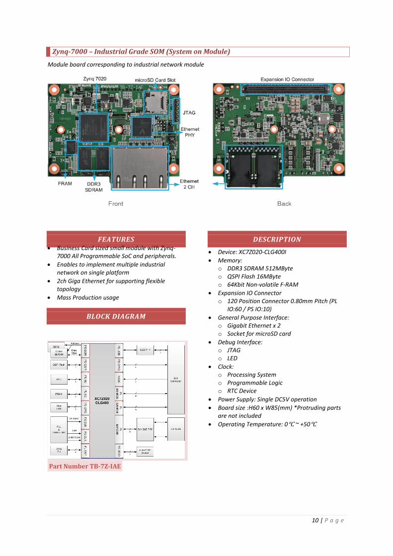
Zynq-7000 – Industrial Grade SOM (System on Module)
Module board corresponding to industrial network module
FEATURES Business Card sized small module with Zynq-
7000 All Programmable SoC and peripherals.
Enables to implement multiple industrial network on single platform
2ch Giga Ethernet for supporting flexible topology
Mass Production usage
BLOCK DIAGRAM
Part Number TB-7Z-IAE
DESCRIPTION Device: XC7Z020-CLG400I
Memory: o DDR3 SDRAM 512MByte o QSPI Flash 16MByte o 64Kbit Non-volatile F-RAM
Expansion IO Connector o 120 Position Connector 0.80mm Pitch (PL
IO:60 / PS IO:10)
General Purpose Interface: o Gigabit Ethernet x 2 o Socket for microSD card
Debug Interface: o JTAG o LED
Clock: o Processing System o Programmable Logic o RTC Device
Power Supply: Single DC5V operation
Board size :H60 x W85(mm) *Protruding parts are not included
Operating Temperature: 0℃ ~ +50℃

11 | P a g e
Zynq-7000 – Industrial Grade SOM (System On Module) Development Kit
TB-7Z-IAE Development Kit
Use Case
This reference design enables greater development
time shortening for machine vision systems.
Part Number TB-7Z-ISDK
Description Daughter board:TB-7Z-IAE
Device :XC6SLX45-FGG484
Memory : o DDR2 SDRAM 1Gbit o QSPI Flash 64Mbit
Interface: o USB2.0 (Host) o DVI TX o CameraLink Base o 10/100Mbps Ethernet (RJ45) o CAN (D-SUB9) o RS-232C (D-SUB9) o PMOD x2 o XADC (Pin header)
Debug Interface o ARM JTAG 20 pin header o 10pin header for XILINX Cable o Push Switch, DIP Switch, LED, Rotary Switch
Power (AC adopter)
Board size:H110 x W185(mm)
Reference Design
Machine vision

12 | P a g e
FPGA Mezzanine Cards (FMC)
High Pin Count FMC

13 | P a g e
Low Pin Count FMC

14 | P a g e
IP Cores
V-by-ONE HS IP Core
MECHATROLINK – III Master IP Core

15 | P a g e
3D ToF Camera Module
What is TOF Camera?
The TOF --Time of Flight-- camera, it is the depth
image sensing camera that can measure the depth
distance at each pixel by the reflection time from
the near-infrared light of objects that have been
pulse emission. TOF camera is the promising
solution that can be applied to a variety of
applications that require three-dimensional
information in the industrial field.
Description Controller of TOF sensor module is implemented in
ARM internal organs FPGA (Zynq-7000 All
Programmable SoC). It is possible to customize
over the details on the user side. Easily build a PC
based evaluation environment and host processing
system by utilizing the sample application and SDK
provided.
Block Diagram
Features
Object recognition
Extract only the object to be located at a particular
distance. It can be realized easy to separate from
the background of the necessary parts. It improves
and reduces the recognition accuracy of the
identification process.
Part Number TB-7Z-TCDK-GC2/TB-7Z-
TCDK-GC3
Object surveillance
It can be detected an object cannot be detected
from the visible image by using depth image. It is
useful for detection and warning of intrusion into
the area.
Form recognition
It is possible to recognize the shape of the object
simply by shooting a three-dimensional shape and
texture (colour pattern) without parallax.

16 | P a g e
Fujitsu Electronics Europe GmbH European Headquarters Tel: +49 (0) 61 03 69 00 Fax: +49 (0) 61 03 69 01 22 [email protected] Address: Pittlerstrasse 47 63225 Langen Germany