PRODUCT OVERVIEW Refl owable Thermal Protection … · applications, including shock, vibration,...
7
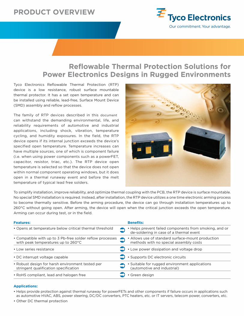
Applications: • Helps provide protection against thermal runaway for powerFETs and other components if failure occurs in applications such as automotive HVAC, ABS, power steering, DC/DC converters, PTC heaters, etc. or IT servers, telecom power, converters, etc. • Other DC thermal protection Features: Benefits: • Opens at temperature below critical thermal threshold • Helps prevent failed components from smoking, and or de-soldering in case of a thermal event • Compatible with up to 3 Pb-free solder reflow processes with peak temperatures up to 260°C • Allows use of standard surface-mount production methods with no special assembly costs • Low series resistance • Low power dissipation and voltage drop • DC interrupt voltage capable • Supports DC electronic circuits • Robust design for harsh environment tested per stringent qualification specification • Suitable for rugged environment applications (automotive and industrial) • RoHS compliant, lead and halogen free • Green design PRODUCT OVERVIEW Reflowable Thermal Protection Solutions for Power Electronics Designs in Rugged Environments Tyco Electronics Reflowable Thermal Protection (RTP) device is a low resistance, robust surface mountable thermal protector. It has a set open temperature and can be installed using reliable, lead-free, Surface Mount Device (SMD) assembly and reflow processes. The family of RTP devices described in this document can withstand the demanding environmental, life, and reliability requirements of automotive and industrial applications, including shock, vibration, temperature cycling, and humidity exposures. In the field, the RTP device opens if its internal junction exceeds the device’s specified open temperature. Temperature increases can have multiple sources, one of which is component failure (i.e. when using power components such as a powerFET, capacitor, resistor, triac, etc.). The RTP device open temperature is selected so that the device does not open within normal component operating windows, but it does open in a thermal runaway event and before the melt temperature of typical lead free solders. To simplify installation, improve reliability, and optimize thermal coupling with the PCB, the RTP device is surface mountable. No special SMD installation is required. Instead, after installation, the RTP device utilizes a one time electronic arming process to become thermally sensitive. Before the arming procedure, the device can go through installation temperatures up to 260°C without going open. After arming, the device will open when the critical junction exceeds the open temperature. Arming can occur during test, or in the field.
Transcript of PRODUCT OVERVIEW Refl owable Thermal Protection … · applications, including shock, vibration,...
Applications:
• Helps provide protection against thermal runaway for powerFETs and other components if failure occurs in applications such as automotive HVAC, ABS, power steering, DC/DC converters, PTC heaters, etc. or IT servers, telecom power, converters, etc.
• Other DC thermal protection
Features: Benefi ts:
• Opens at temperature below critical thermal threshold • Helps prevent failed components from smoking, and or de-soldering in case of a thermal event
• Compatible with up to 3 Pb-free solder refl ow processes with peak temperatures up to 260°C
• Allows use of standard surface-mount production methods with no special assembly costs
• Low series resistance • Low power dissipation and voltage drop
• DC interrupt voltage capable • Supports DC electronic circuits
• Robust design for harsh environment tested per stringent qualifi cation specifi cation
• Suitable for rugged environment applications (automotive and industrial)
• RoHS compliant, lead and halogen free • Green design
PRODUCT OVERVIEW
Refl owable Thermal Protection Solutions for Power Electronics Designs in Rugged Environments
Tyco Electronics Refl owable Thermal Protection (RTP)
device is a low resistance, robust surface mountable
thermal protector. It has a set open temperature and can
be installed using reliable, lead-free, Surface Mount Device
(SMD) assembly and refl ow processes.
The family of RTP devices described in this document
can withstand the demanding environmental, life, and
reliability requirements of automotive and industrial
applications, including shock, vibration, temperature
cycling, and humidity exposures. In the field, the RTP
device opens if its internal junction exceeds the device’s
specified open temperature. Temperature increases can
have multiple sources, one of which is component failure
(i.e. when using power components such as a powerFET,
capacitor, resistor, triac, etc.). The RTP device open
temperature is selected so that the device does not open
within normal component operating windows, but it does
open in a thermal runaway event and before the melt
temperature of typical lead free solders.
To simplify installation, improve reliability, and optimize thermal coupling with the PCB, the RTP device is surface mountable.
No special SMD installation is required. Instead, after installation, the RTP device utilizes a one time electronic arming process
to become thermally sensitive. Before the arming procedure, the device can go through installation temperatures up to
260°C without going open. After arming, the device will open when the critical junction exceeds the open temperature.
Arming can occur during test, or in the fi eld.
us082978
Typewritten Text

Failed powerFETor other heat source
P1
PTH
ARM
+–
Lo
ad
1
Batt
ery
ThermalCoupling
RTP
Typical Application Block Diagram
Sample Arming Options
Pin Confi guration & Description Pad Layout Recommendations
Defi nition Of Terms / Device Block Diagram
Method of Operation – Electronic Arming
2
Junction The internal interface which must achieve the “Open Temperature” for the RTP device to open thermally after arming. This interface (thermal element) is located directly above the PTH pad.
Open Temp The device will open when the junction temperature achieves this value.
IARM and RARM Current and resistance levels measured between the ARM pin and either theP1 or PTH pin. These values are relevant only pre device arming.
RPP and IPP Current and resistance levels measured between the P1 and PTH pins.
The RTP device is a unique thermal protector. It can be refl owed at temperatures up to 260°C without opening, yet in operation it will open at temperatures well below 260°C. To achieve this functionality, the RTP device uses an electronic arming mechanism.
Electronic arming must be done after refl ow, and can be done during fi nal test.
The device is armed by sending a specifi ed arming current through the ARM pin of the device. Arming is a time- & current-dependent event. Arming times vs. current are provided in the “Arming Characteristics” section of this data sheet. Current can fl ow in either direction through the ARM pin.
Prior to arming, RARM should have resistance levels as specifi ed in the “Arming Characteristics” section. Once armed, the ARM pin will be electrically open relative to the P1 or PTH pins.
Arming has been successful once RARM exceeds the post-arming minimum resistance specifi ed in the “Arming Characteristics” section. RTP devices must be armed individually and cannot be armed simultaneously in series.
Once “armed”, the RTP device will permanently open when the device junction achieves its specifi ed opening temperature.
Although multiple options exist, below is one simple arming option.
During Test Current Flow Description
P1
PTH
ARM
RTPPowerFET
TestPoint 1
TestPoint 2
PTH ARM = Arming
ARM pin connected between two test points
In this case, Test Point 1 is left “fl oating”, and arming can occur during test, at a user defi ned time, by connecting to the Test Points and applying suffi cient current (IARM) between Test Point 1 and Test Point 2 until the device is armed.
Pin Description
PinNumber
PinName Pin Function
1 P1Power I/O pin (Main power current path)
2 PTH
Thermally sensitive power I/O pin - Intended to share protected component heat sink
3 ARM Electronic arming pin
ARMP
THP
1
Pin Configuration (Bottom View of Device)
1.42
1.32
1.24
1.12 3.48
1.83
9.64
2.49
1.79
Pad Dimensions in mm(Top View – Through Component)
ARM
P1
RARM
PTH
IPP
IARM
ThermalProtectionDeviceElement
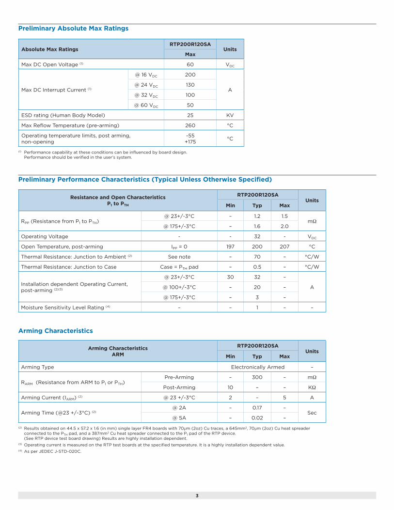
Preliminary Absolute Max Ratings
Preliminary Performance Characteristics (Typical Unless Otherwise Specifi ed)
3
Absolute Max RatingsRTP200R120SA
UnitsMax
Max DC Open Voltage (1) 60 VDC
Max DC Interrupt Current (1)
@ 16 VDC 200
A@ 24 VDC 130
@ 32 VDC 100
@ 60 VDC 50
ESD rating (Human Body Model) 25 KV
Max Refl ow Temperature (pre-arming) 260 °C
Operating temperature limits, post arming, non-opening
-55+175
°C
(1) Performance capability at these conditions can be infl uenced by board design. Performance should be verifi ed in the user’s system.
Resistance and Open CharacteristicsP1 to PTH
RTP200R120SAUnits
Min Typ Max
RPP (Resistance from P1 to PTH)@ 23+/-3°C – 1.2 1.5
mΩ@ 175+/-3°C – 1.6 2.0
Operating Voltage - - 32 - VDC
Open Temperature, post-arming IPP = 0 197 200 207 °C
Thermal Resistance: Junction to Ambient (2) See note – 70 – °C/W
Thermal Resistance: Junction to Case Case = PTH pad – 0.5 – °C/W
Installation dependent Operating Current, post-arming (2)(3)
@ 23+/-3°C 30 32 –
A@ 100+/-3°C – 20 –
@ 175+/-3°C – 3 –
Moisture Sensitivity Level Rating (4) – – 1 – –
Arming Characteristics
Arming CharacteristicsARM
RTP200R120SAUnits
Min Typ Max
Arming Type Electronically Armed –
RARM (Resistance from ARM to P1 or PTH)Pre-Arming – 300 – mΩ
Post-Arming 10 – – KΩ
Arming Current (IARM) (2) @ 23 +/-3°C 2 – 5 A
Arming Time (@23 +/-3°C) (2)@ 2A – 0.17 –
Sec@ 5A – 0.02 –
(2) Results obtained on 44.5 x 57.2 x 1.6 (in mm) single layer FR4 boards with 70µm (2oz) Cu traces, a 645mm2, 70µm (2oz) Cu heat spreader connected to the PTH pad, and a 387mm2 Cu heat spreader connected to the P1 pad of the RTP device.
(See RTP device test board drawing) Results are highly installation dependent.(3) Operating current is measured on the RTP test boards at the specifi ed temperature. It is a highly installation dependent value.(4) As per JEDEC J-STD-020C.

4
Typical Electrical Performance Characteristics
Typical Resistance (RPP) Vs Temperature(Passive Testing)
RP
P (
mO
hm
s)
Temperature (°C)
2.0
1.5
1.0
0.5
0.00 50 100 150 200
RTP200R120SA
INSTALLATION DEPENDENT PERFORMANCE CHARACTERISTICS
Note: Results were obtained on 44.5 x 57.2 x 1.6 (in mm) single layer FR4 boards with 2mOhms, 70µm (2oz) Cu traces, and a
645mm2, 70µm (2oz) Cu heat spreader connected to the PTH pad of the RTP device. (See RTP device test board drawing)
Results will vary based on user’s confi guration and should be validated by the user in the end system.
Typical Operating Current Vs Temperature(Mounted as described in above notice)
Op
era
tin
g C
urr
en
t (A
)
Temperature (°C)
40
30
20
10
00 50 100 150 250200
RTP200R120SA
Typical Open Current (IPP Open) Vs Timefor RTP200R120SA Device
(Mounted as described in above notice)
Tim
e (
sec)
Open Current (A)
1.0
0.1
00 50 100 150 200
25°C
100°C
150°C
250
Typical Arming Time @ 23 +/-3°C(Mounted as described in above notice)
Arm
ing
Tim
e (
sec)
Activation Current - IARM (A)
1.0
0.1
02.0 3.0 4.0 5.0
RTP200R120SA
P1 PTH
TY
CO
ELE
CTR
ON
ICS
T4
225 R
ev.2
JA
N 2
010
FR
4 R
TP
Test
Bo
ard
Cu 2
.0 o
z
4x .1004x .100
.039 (1.00)
.039 (1.00)
3X ø.030±.003AFTER PLATING
PLATED THRU HOLE
4X ø.065±.003NON PLATED HOLE
1.750
2.250
ARM
PTH pad area = 661mm2, P1 pad area = 393mm2, ARM pad area = 169mm2
Test Board: 44.5 x 57.2 x 1.6 mm, 70µm (2oz) Cu
5
Mechanical Dimensions
Material Construction
Recommended Refl ow Profi le
Profi le Feature Pb-Free Assembly
Average Ramp-Up Rate (TsMAX to Tp) 3°C/second max.
Preheat
• Temperature Min (TsMIN)
• Temperature Max (TsMAX)
• Time (tsMIN to tsMAX)
150°C
200°C
60-180 seconds
Time maintained above:
• Temperature (TL)
• Time (tL)
217°C
60-150 seconds
Peak/Classifi cation Temperature (Tp) 260°C
Time within 5°C of actual Peak Temperature
Time (tp) 20-24 seconds
Ramp-Down Rate 6°C/second max.
Time 25°C to Peak Temperature 8 minutes max.
Critical ZoneTL to TpRamp up
t 25°C to Peak
Reflow Profile Time
Ramp downts
Preheat
TsMAX
TL
Tptp
25
TsMIN
tL
Tem
pe
ratu
re
Classifi cation Refl ow Profi les
RoHS Compliant ELV Compliant Pb-Free Halogen Free*
Refl ow Profi le
11.80
1.12 1.451.37
1.45 1.04
6.15
Dimension TypicalUnless Otherwise Noted
5.38
RTP200R120SAUnits
Min Max
Height 5.95 6.25 mm
Length 11.65 11.90 mm
Width 5.15 5.40 mm
Directive 2002/95/ECCompliant
Directive 2000/53/ECCompliant Pb HF
* Halogen Free refers to: Br≤900ppm, Cl≤900ppm, Br+Cl≤1500ppm.
6
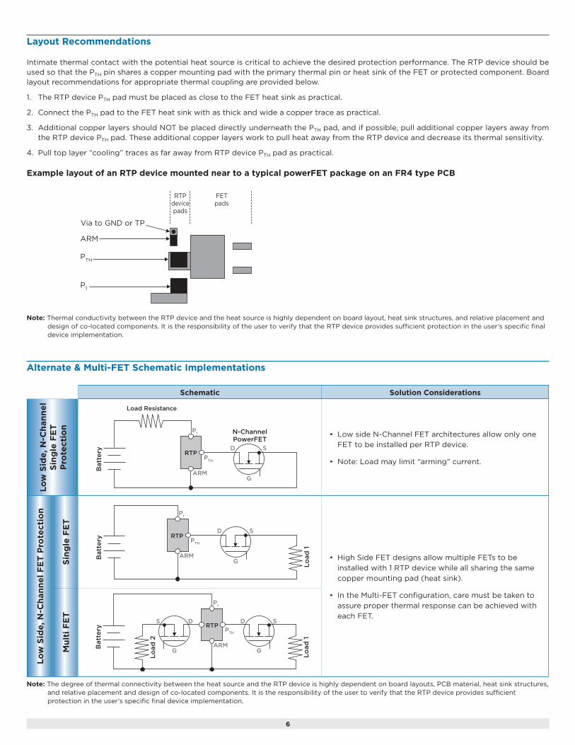
Layout Recommendations
Alternate & Multi-FET Schematic Implementations
Intimate thermal contact with the potential heat source is critical to achieve the desired protection performance. The RTP device should be used so that the PTH pin shares a copper mounting pad with the primary thermal pin or heat sink of the FET or protected component. Board layout recommendations for appropriate thermal coupling are provided below.
1. The RTP device PTH pad must be placed as close to the FET heat sink as practical.
2. Connect the PTH pad to the FET heat sink with as thick and wide a copper trace as practical.
3. Additional copper layers should NOT be placed directly underneath the PTH pad, and if possible, pull additional copper layers away from the RTP device PTH pad. These additional copper layers work to pull heat away from the RTP device and decrease its thermal sensitivity.
4. Pull top layer “cooling” traces as far away from RTP device PTH pad as practical.
Example layout of an RTP device mounted near to a typical powerFET package on an FR4 type PCB
Note: Thermal conductivity between the RTP device and the heat source is highly dependent on board layout, heat sink structures, and relative placement and design of co-located components. It is the responsibility of the user to verify that the RTP device provides suffi cient protection in the user’s specifi c fi nal device implementation.
Note: The degree of thermal connectivity between the heat source and the RTP device is highly dependent on board layouts, PCB material, heat sink structures, and relative placement and design of co-located components. It is the responsibility of the user to verify that the RTP device provides suffi cient protection in the user’s specifi c fi nal device implementation.
Schematic Solution Considerations
Lo
w S
ide
, N
-Ch
an
ne
lS
ing
le F
ET
P
rote
cti
on
N-ChannelPowerFET
Load Resistance
P1
PTH
ARM
D S
G
Batt
ery RTP
• Low side N-Channel FET architectures allow only one
FET to be installed per RTP device.
• Note: Load may limit “arming” current.
Lo
w S
ide
, N
-Ch
an
ne
l F
ET
Pro
tecti
on
Sin
gle
FE
T
RTP
P1
PTH
ARM
D S
G
Batt
ery
Lo
ad
1
• High Side FET designs allow multiple FETs to be
installed with 1 RTP device while all sharing the same
copper mounting pad (heat sink).
• In the Multi-FET confi guration, care must be taken to
assure proper thermal response can be achieved with
each FET.
Mu
lti
FE
T
P1
PTH
ARM
D S
G
Batt
ery
Lo
ad
1
Lo
ad
2
DS
G
RTP
ARM
Via to GND or TP
RTPdevicepads
FETpads
PTH
P1
Qualifi cation Testing
The Qualification testing plan for this series of RTP devices is built upon AEC automotive grade testing for ICs (AEC-Q100), discrete semiconductors (AEC-Q101), and passive components (AEC-Q200), with the intent to demonstrate survivability to the most stringent of the relevant requirements. Tyco Electronics requires that at least 3 lots of production devices pass internal qualification* tests prior to full production release.Contact Tyco Electronics for updated qualification status and detailed procedures.
*A specific list of tests and conditions is available upon request.
TE (logo) and Tyco Electronics are trademarks. Other logos, product and Company names mentioned herein may be trademarks of their respective owners. All information, including illustrations, is believed to be reliable. Users, however, should independently evaluate the suitability of each product for their application. Tyco Electronics Corporation makes no warranties as to the accuracy or completeness of the information, and disclaims any liability regarding its use. Tyco Electronics’ only obligations are those in the Tyco Electronics Standard Terms and Conditions of Sale for this product, and in no case will Tyco Electronics be liable for any incidental, indirect, or consequential damages arising from the sale, resale, use, or misuse of the product. Specifi cations are subject to change without notice. In addition, Tyco Electronics reserves the right to make changes without notifi cation to Buyer—to materials or processing that do not affect compliance with any applicable specifi cation.
© 2010 Tyco Electronics Corporation. All rights reserved. RCP0095E.1110
Circuit Protection Products308 Constitution DriveMenlo Park, CA USA 94025-1164Tel : (800) 227-7040, (650) 361-6900Fax : (650) 361-4600Email : [email protected]
www.circuitprotection.comwww.circuitprotection.com.hk (Chinese)www.tycoelectronics.com/japan/bu/circuitprotection (Japanese)