
Product Data Sheet - Mouser Electronics Technologies Oy Page 7 of 29 2 Pinout and Terminal...
29
BLE121LR DATA SHEET Monday, 12 May 2014 Version 1.1
Transcript of Product Data Sheet - Mouser Electronics Technologies Oy Page 7 of 29 2 Pinout and Terminal...

BLE121LR DATA SHEET
Monday, 12 May 2014
Version 1.1

Bluegiga Technologies Oy
Copyright © 2000-2014 Bluegiga Technologies
All rights reserved.
Bluegiga Technologies assumes no responsibility for any errors which may appear in this manual. Furthermore, Bluegiga Technologies reserves the right to alter the hardware, software, and/or specifications detailed here at any time without notice and does not make any commitment to update the information contained here. Bluegiga’s products are not authorized for use as critical components in life support devices or systems.
The WRAP is a registered trademark of Bluegiga Technologies
The Bluetooth trademark is owned by the Bluetooth SIG Inc., USA and is licensed to Bluegiga Technologies. All other trademarks listed herein are owned by their respective owners.

Bluegiga Technologies Oy
VERSION HISTORY
Version Comment
1.1 First release

Bluegiga Technologies Oy
TABLE OF CONTENTS
1 BLE121LR Product numbering ......................................................................................................................6
2 Pinout and Terminal Description ...................................................................................................................7
2.1 I/O Ports .............................................................................................................................................. 10
2.1.1 I/O Configurations ........................................................................................................................ 10
2.1.2 Reserved I/O’s ............................................................................................................................. 10
2.2 UART ................................................................................................................................................... 10
3 Electrical Characteristics ............................................................................................................................ 11
3.1 Absolute Maximum Ratings ................................................................................................................ 11
3.2 Recommended Operating Conditions ................................................................................................. 11
3.3 DC Characteristics .............................................................................................................................. 11
3.4 Current Consumption .......................................................................................................................... 12
3.5 RF Characteristics ............................................................................................................................... 13
4 Physical Dimensions .................................................................................................................................. 17
5 Power-On Reset and Brownout Detector ................................................................................................... 19
6 Design Guidelines ...................................................................................................................................... 20
6.1 General Design Guidelines ................................................................................................................. 20
6.2 Layout Guide Lines ............................................................................................................................. 20
6.3 BLE121LR-A Layout Guide ................................................................................................................. 21
7 Soldering Recommendations ..................................................................................................................... 23
8 Block diagram ............................................................................................................................................. 24
9 Certifications ............................................................................................................................................... 27
9.1 Bluetooth ............................................................................................................................................. 27
9.2 FCC ..................................................................................................................................................... 27
9.3 IC ......................................................................................................................................................... 27
9.3.1 IC .................................................................................................................................................. 27
9.4 CE ....................................................................................................................................................... 28
9.5 MIC Japan ........................................................................................................................................... 28
9.6 KCC (Korea) ........................................................................................................................................ 28
10 Contact Information................................................................................................................................. 29

Bluegiga Technologies Oy
BLE121LR Bluetooth® Smart Module
DESCRIPTION
BLE121LR is a Bluetooth Smart Long Range
module targeted for Bluetooth Smart
applications where the best possible RF performance and range are required. At +8 dBm TX power and -98 dBm sensitivity BLE121LR has best-in-class RF performance
and can provide Bluetooth Smart connectivity up to 450 meters. BLE121LR integrates all
features required for a Bluetooth Smart
application: Bluetooth radio, software stack
and GATT based profiles. and it can also host end user applications, which means no external micro controller is required in size, price or power constrained devices.
BLE121LRBluetooth Smart module also has flexible hardware interfaces to connect to different peripherals or sensors. Although
BLE121LR Bluetooth Smart Long Range
Module is target for applications requiring high RF performance, it is still has relatively low power consumption and can be power using a standard 3V coin cell batteries.
APPLICATIONS:
Smart home accessories
beacon devices
Health and fitness sensors
Medical sensors
iPhone and iPad accessories
Security and proximity tags
KEY FEATURES:
Bluetooth v. 4.0 Single Mode Compliant
o Master and slave modes
o Up to eight connections
Integrated Bluetooth Smart Stack
o GAP, ATT and GATT
o Bluetooth Smart profiles
Best-in-Class RF Performance
o Transmit power : +8 dBm
o Receiver sensitivity: -98 dBm
o Range up to 450 meters
Low Current Consumption
o Transmit: 36 mA (+8 dBm)
o Receive: 33 mA (-98 dBm)
o Power mode 3: 0.5 uA
Flexible Peripheral Interfaces
o UART and SPI
o I2C, PWM and GPIO
o 12-bit ADC
Host Interfaces:
o UART
Programmable 8051 Processor for
Stand-alone Operation
o Simple Bluegiga BGScriptTM
scripting language for quick
application development
o Bluegiga Profile ToolkitTM
allowing the quick development
of GATT based profiles
Dimensions: 14.7 x 13.0 x 1.8 mm
Bluetooth, CE, FCC, IC, South Korea
and Japan qualified

Bluegiga Technologies Oy
Page 6 of 29
1 BLE121LR Product numbering
Available products and product codes
Product code Description
BLE121LR-A-M256K BLE121LR with an embedded chip antenna and with 256k internal flash
Bluegiga Technologies Oy
Page 7 of 29
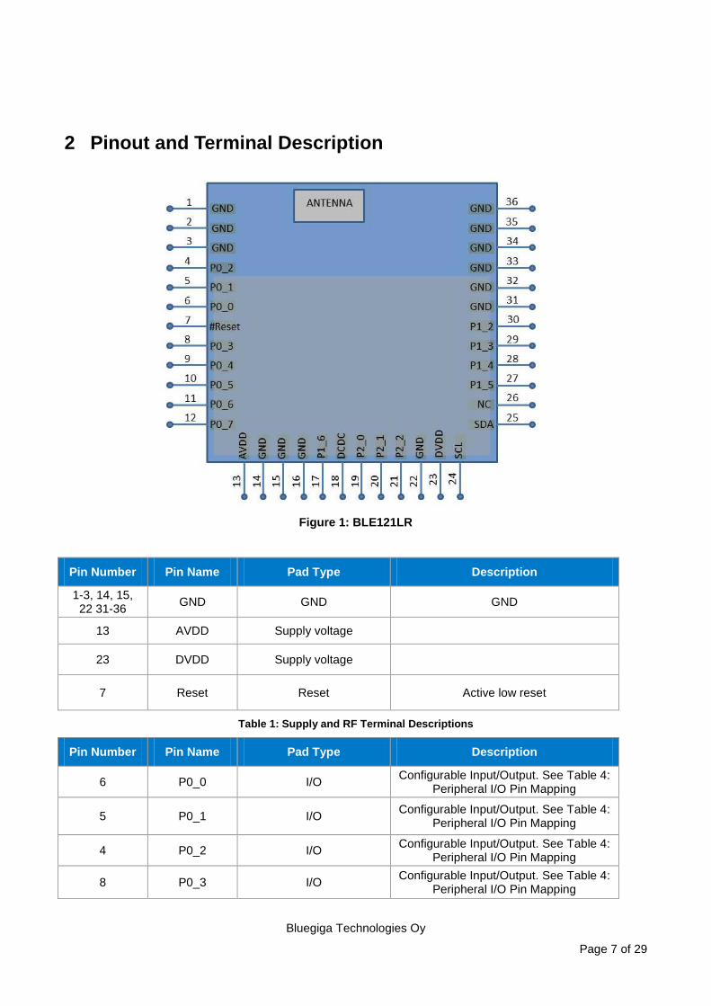
2 Pinout and Terminal Description
Figure 1: BLE121LR
Pin Number Pin Name Pad Type Description
1-3, 14, 15, 22 31-36
GND GND GND
13 AVDD Supply voltage
23 DVDD Supply voltage
7 Reset Reset Active low reset
Table 1: Supply and RF Terminal Descriptions
Pin Number Pin Name Pad Type Description
6 P0_0 I/O Configurable Input/Output. See Table 4:
Peripheral I/O Pin Mapping
5 P0_1 I/O Configurable Input/Output. See Table 4:
Peripheral I/O Pin Mapping
4 P0_2 I/O Configurable Input/Output. See Table 4:
Peripheral I/O Pin Mapping
8 P0_3 I/O Configurable Input/Output. See Table 4:
Peripheral I/O Pin Mapping

Bluegiga Technologies Oy
Page 8 of 29
9 P0_4 I/O Configurable Input/Output. See Table 4:
Peripheral I/O Pin Mapping
10 P0_5 I/O Configurable Input/Output. See Table 4:
Peripheral I/O Pin Mapping
11 P0_6 I/O Configurable Input/Output. See Table 4:
Peripheral I/O Pin Mapping
12 P0_7 I/O Configurable Input/Output. See Table 4:
Peripheral I/O Pin Mapping
30 P1_2 I/O Configurable Input/Output. See Table 4:
Peripheral I/O Pin Mapping
29 P1_3 I/O Configurable Input/Output. See Table 4:
Peripheral I/O Pin Mapping
28 P1_4 I/O Configurable Input/Output. See Table 4:
Peripheral I/O Pin Mapping
27 P1_5 I/O Configurable Input/Output. See Table 4:
Peripheral I/O Pin Mapping
17 P1_6 I/O Configurable Input/Output. See Table 4:
Peripheral I/O Pin Mapping
19 P2_0 I/O Configurable Input/Output. See Table 4:
Peripheral I/O Pin Mapping
20 P2_1 I/O Configurable Input/Output. See Table 4:
Peripheral I/O Pin Mapping
21 P2_2 I/O Configurable Input/Output. See Table 4:
Peripheral I/O Pin Mapping
Table 2: Configurable I/O Terminals
Pin Number Pin Name Pad Type Description
24 SCL I2C clock
25 SDA I2C data
18 DCDC_CNTRL Output On / by-pass control for an external
DCDC converter
Table 3: Non-configurable Terminals

Bluegiga Technologies Oy
Page 9 of 29
HARDWARE.XML Example (*
7 6 5 4 3 2 1 0 7 6 5 4 3 2 1 0 2 1 0
A7 A6 A5 A4 A3 A2 A1 A0
Alt.1 C SS MO MI <usart channel="0" mode="spi_master" alternate="1" ...
Alt.2 MO MI C SS <usart channel="0" mode="spi_master" alternate="2" ...
Alt.1 RT CT TX RX <usart channel="0" mode="uart" alternate="1" ...
Alt.2 TX RX RT CT <usart channel="0" mode="uart" alternate="2" ...
Alt.1 MI MO C SS <usart channel="1" mode="spi_master" alternate="1" ...
Alt.2 MO C SS <usart channel="1" mode="spi_master" alternate="2" ...
Alt.1 RX TX RT CT <usart channel="1" mode="uart" alternate="1" ...
Alt.2 TX RT CT <usart channel="1" mode="uart" alternate="2" ...
Alt.1 4 3 2 1 0 <timer index="1" alternate="1" ...
Alt.2 3 4 0 <timer index="1" alternate="2" ...
Alt.1 1 0 <timer index="3" alternate="1" ...
Alt.2 0 <timer index="3" alternate="2" ...
Alt.1 <timer index="4" alternate="1" ...
Alt.2 0 <timer index="4" alternate="2" ...
DC DD
5 4 3 2
P1PERIPHERAL /
FUNCTION
P2
USART 0 SPI (**
R
E
S
E
R
V
E
D
R
E
S
E
R
V
E
D
D
C
D
C
C
O
N
T
R
O
L
DEBUG
OBSSEL
ADC
TIMER 3
TIMER 4
P0
USART 0 UART
USART 1 SPI (**
USART 1 UART
TIMER 1
*) Refer to BLE Configuration Guide for detailed settings
**) SS is the slave select signal when BLE121LR is set as SPI slave. When set as SPI master, any available I/O can be used as chip select signal of BLE121LR
NOTE: Pins configured as peripheral I/O signals do not have pull-up / -down capability
Table 4: Peripheral I/O Pin Mapping

Bluegiga Technologies Oy
Page 10 of 29
2.1 I/O Ports
2.1.1 I/O Configurations
Each I/O port can be configured as an input or output. When configured as input, each I/O port can also be configured with internal pull-up, pull-down or tri-state. Pull-down or pull-up can only be configured to whole port, not individual pins. Unused I/O pins should have defined level and not be floating. See the BLE Configuration Guide for more information about the configuration.
During reset the I/O pins are configured as inputs with pull-ups.
Note: Pins configured as peripheral I/O signals do not have pull-up / -down capability
2.1.2 Reserved I/O’s
The high current driving pins P1_0 and P1_1 are reserved for the internal RF front end control. These pins are not exposed in BLE121LR and they can’t be used for application purposes.
P1_7 is also used for the RF front end control but as an output it can be used to control the external DCDC for lowering the peak current drawn from the battery. The function of P1_7 can’t be altered. If external DCD is not used then P1_7 should be left not connected.
2.2 UART
UART baud rate can be configured up 2 Mbps. See the BLE Configuration Guide for more information. Following table lists commonly used baud rates for BLE121LR
Baud rate (bps) Error (%)
2400 0.14
4800 0.14
9600 0.14
14 400 0.03
19 200 0.14
28 800 0.03
38 400 0.14
57 600 0.03
76 800 0.14
115 200 0.03
230 400 0.03
Table 5: Commonly used baud rates for BLE121LR

Bluegiga Technologies Oy
Page 11 of 29
3 Electrical Characteristics
3.1 Absolute Maximum Ratings
Note: These are absolute maximum ratings beyond which the module can be permanently damaged. These are not
maximum operating conditions. The maximum recommended operating conditions are in the Table 7.
Rating Min Max Unit
Storage Temperature -40 +85 °C
AVDD, DVDD -0.3 3.9 V
Other Terminal Volatages VSS-0.4 VDD+0.4 V
Table 6: Absolute Maximum Ratings
3.2 Recommended Operating Conditions
Rating Min Max Unit
Operationg Temperature Range -40 +85 °C
AVDD, DVDD (*,**,*** 2.0 3.6 V
Table 7: Recommended Operating Conditions
*) All supply nets must have the same voltage **) Supply voltage noise should be less than 10mVpp. Excessive noise at the supply voltage will reduce the
RF performance. ***) The supply voltage has an impact on the TX power, see Figure 7.
3.3 DC Characteristics
Parameter Test Conditions Min Typ Max Unit
Logic-0 input voltage 0.5 V
Logic-1 input voltage DVDD =3V0 2.5 V
Logic-0 input current Input equals 0V -50 50 nA
Logic-1 input current Input equals VDD -50 50 nA
I/O pin pull-up and pull-down resistors 20 kΩ
For detailed I/O terminal characteristic and timings refer to the CC2541 datasheet available in (http://www.ti.com/lit/ds/symlink/cc2541.pdf)
Table 8: DC Characteristic

Bluegiga Technologies Oy
Page 12 of 29
3.4 Current Consumption
Power mode hardware.xml Min Typ Max Unit
Transmit
<txpower power = ”1”/> <slow clock enable = ”true”/>
25 mA
<txpower power = ”9”/> <slow clock enable = ”true”/>
36 mA
<txpower power = ”9”/> <slow clock enable = ”false”/>
38 mA
Receive <slow clock enable = ”true”/> 28 mA
<slow clock enable = ”false”/> 33 mA
Power mode 1 2.7 mA
Power mode 2 1.3 µA
Power mode 3 0.5 µA
Figure 2: BLE121LR TX peak current as a function of the setting in the HW configuration file
Figure 3: BLE121LR TX peak current as a function of hardware.xml TXP setting (Example: <txpower
power="9" bias="5" />)
Bluegiga Technologies Oy
Page 13 of 29
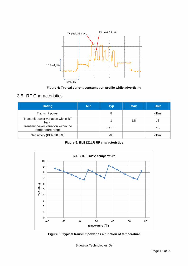
1ms/div
16.7mA/div
TX peak 36 mA RX peak 28 mA
Figure 4: Typical current consumption profile while advertising
3.5 RF Characteristics
Rating Min Typ Max Unit
Transmit power 8 dBm
Transmit power variation within BT band
1 1.8 dB
Transmit power variation within the temperature range
+/-1.5 dB
Sensitivity (PER 30.8%) -98 dBm
Figure 5: BLE121LR RF characteristics
Figure 6: Typical transmit power as a function of temperature

Bluegiga Technologies Oy
Page 14 of 29
Figure 7: BLE121LR transmit power as a function of supply voltage
Figure 8: BLE121LR TX power as a function of the setting in the HW configuration file (Example: <txpower power="9" bias="5" />)

Bluegiga Technologies Oy
Page 15 of 29
Figure 9: Radiation pattern of BLE121LR when mounted to the DKBLE
Figure 10: Radiation pattern of BLE121LR when mounted to the DKBLE

Bluegiga Technologies Oy
Page 16 of 29
Figure 11: Radiation pattern of BLE121LR when mounted to the DKBLE

Bluegiga Technologies Oy
Page 17 of 29
4 Physical Dimensions
PINOUT AND DIMENSIONS OF BLE121LR
Figure 12: Footprint of BLE121LR (top view)
Physical Dimensions of BLE121LR
14
.7 m
m
13.0 mm
4.8 mm
6.8 mm
8.4 mm
13
.7 m
m
3.9 mm
1.8 mm 1.8 mm
1.9 mm
Figure 13: Physical dimensions (top view)
Physical Dimensions of BLE121LR
14
.7 m
m
13.0 mm
4.8 mm
6.8 mm
8.4 mm
13
.7 m
m
3.9 mm
1.8 mm 1.8 mm
1.9 mm
Figure 14: Physical dimensions (side view)

Bluegiga Technologies Oy
Page 18 of 29
Figure 15: Recommended land pattern for BLE121LR-A

Bluegiga Technologies Oy
Page 19 of 29
5 Power-On Reset and Brownout Detector
BLE121LR includes a power-on reset (POR), providing correct initialization during device power on. It also includes a brownout detector (BOD) operating on the regulated 1.8-V digital power supply only. The BOD protects the memory contents during supply voltage variations which cause the regulated 1.8-V power to drop below the minimum level required by digital logic, flash memory, and SRAM. When power is initially applied, the POR and BOD hold the device in the reset state until the supply voltage rises above the power-on-reset and brownout voltages.

Bluegiga Technologies Oy
Page 20 of 29
6 Design Guidelines
6.1 General Design Guidelines
BLE121LR can be used directly with a coin cell battery. Due to relatively high internal resistance of a coin cell battery it is recommended to place a 100uF capacitor in parallel with the battery. The internal resistance of a coin cell battery is initially in the range of 10 ohms but the resistance increases rapidly as the capacity is used. Basically the higher the value of the capacitor the higher is the effective capacity of the battery and thus the longer the life time for the application. The minimum value for the capacitor depends on the end application and the maximum transmit power used. The leakage current of a 100uF capacitor is in the range of 0.5 uA to 3 uA and generally ceramic capacitors have lower leakage current than tantalum or aluminum electrolytic capacitors.
Optionally TI’s TPS62730 can be used to reduce the current consumption during TX/RX and data processing stages. TPS62730 is an ultra-low power DC/DC converter with by-pass mode and will reduce the current consumption during transmission nominally by ~20% when using 3V coin cell battery.
Figure 16: Example schematic for BLE121LR with a coin cell battery, TPS62730 DCDC converter and an I2C accelerometer
6.2 Layout Guide Lines
Use good layout practices to avoid excessive noise coupling to supply voltage traces or sensitive analog signal traces. If using overlapping ground planes use stitching vias separated by max 3 mm to avoid emission from the edges of the PCB. Connect all the GND pins directly to a solid GND plane and make sure that there is a low impedance path for the return current following the signal and supply traces all the way from start to the end.
A good practice is to dedicate one of the inner layers to a solid GND plane and one of the inner layers to supply voltage planes and traces and route all the signals on top and bottom layers of the PCB. This
Bluegiga Technologies Oy
Page 21 of 29
arrangement will make sure that any return current follows the forward current as close as possible and any loops are minimized.
Layout• Supply voltage
– If possible use solid power plane
– Make sure that solid GND plane follows the traces all the way
– Do not route supply voltage traces across separated GND regions so that the
path for the return current is cut
• MIC input
– Place LC filtering and DC coupling capacitors symmetrically as close to audio
pins as possible
– Place MIC biasing resistors symmetrically as close to microhone as possible.
– Make sure that the bias trace does not cross separated GND regions (DGND ->
AGND) so that the path for the return current is cut. If this is not possible the do
not separate GND regions but keep one solid GND plane.
– Keep the trace as short as possible
Signals
GND
Power
Signals
Recommended PCB layer configuration
Figure 17: Typical 4-layer PCB construction
Overlapping GND layers without
GND stitching vias
Overlapping GND layers with
GND stitching vias shielding the
RF energy
Figure 18: Use of stitching vias to avoid emissions from the edges of the PCB
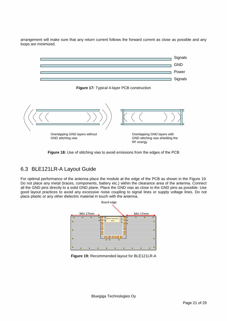
6.3 BLE121LR-A Layout Guide
For optimal performance of the antenna place the module at the edge of the PCB as shown in the Figure 19. Do not place any metal (traces, components, battery etc.) within the clearance area of the antenna. Connect all the GND pins directly to a solid GND plane. Place the GND vias as close to the GND pins as possible. Use good layout practices to avoid any excessive noise coupling to signal lines or supply voltage lines. Do not place plastic or any other dielectric material in touch with the antenna.
Min 17mm Min 17mm
Metal clearancearea
Board edge
Figure 19: Recommended layout for BLE121LR-A

Bluegiga Technologies Oy
Page 22 of 29
Figure 20: Poor layouts for BLE121LR

Bluegiga Technologies Oy
Page 23 of 29
7 Soldering Recommendations
BLE121LR is compatible with industrial standard reflow profile for Pb-free solders. The reflow profile used is dependent on the thermal mass of the entire populated PCB, heat transfer efficiency of the oven and particular type of solder paste used. Consult the datasheet of particular solder paste for profile configurations.
Bluegiga Technologies will give following recommendations for soldering the module to ensure reliable solder joint and operation of the module after soldering. Since the profile used is process and layout dependent, the optimum profile should be studied case by case. Thus following recommendation should be taken as a starting point guide.
- Refer to technical documentations of particular solder paste for profile configurations
- Avoid using more than one flow.
- Reliability of the solder joint and self-alignment of the component are dependent on the solder volume.
Minimum of 150m stencil thickness is recommended.
- Aperture size of the stencil should be 1:1 with the pad size.
- A low residue, “no clean” solder paste should be used due to low mounted height of the component.
Figure 21: Reference reflow profile

Bluegiga Technologies Oy
Page 24 of 29
8 Block diagram
BLE121LR is based on TI’s CC2541 chip. Embedded 32 MHz and 32.678 kHz crystals are used for clock generation. Matched balun and low pass filter provide optimal radio performance with extremely low spurious emissions.
Balun + LPF
Chip antenna
I/O co
ntro
ller
CC2541
I/O
32 MHz XTAL
32.768 kHz XTAL
Clock
Debug interface
8051 CPU core and memory arbitrator
Voltage regulator
SRAM
Flash
Analog comparator
OPAMP
ADC
IRQ controller
DMA
USB
USART 0
USART 1
TIMER 1
TIMER 2
TIMER 3
TIMER 4
Radio arbiterRadio registers
Link layer engineSRAM
ModulatorDemodulator Synth
Receive Transmit
Frequency
synthetisizer
Reset
Power-on reset
2V – 3.6V Reset
PA/LNA BPF
Figure 22: Simplified block diagram of BLE121LR
CPU and Memory
The 8051 CPU core is a single-cycle 8051-compatible core. It has three different memory access buses (SFR, DATA, and CODE/XDATA), a debug interface, and an 18-input extended interrupt unit.
The memory arbiter is at the heart of the system, as it connects the CPU and DMA controller with the physical memories and all peripherals through the SFR bus. The memory arbiter has four memory-access points, access of which can map to one of three physical memories: an SRAM, flash memory, and XREG/SFR registers. It is responsible for performing arbitration and sequencing between simultaneous memory accesses to the same physical memory.
The SFR bus is a common bus that connects all hardware peripherals to the memory arbiter. The SFR bus also provides access to the radio registers in the radio register bank, even though these are indeed mapped into XDATA memory space.
The 8-KB SRAM maps to the DATA memory space and to parts of the XDATA memory spaces. The SRAM is an ultralow-power SRAM that retains its contents even when the digital part is powered off (power modes 2 and 3).
The 256 KB flash block provides in-circuit programmable non-volatile program memory for the device, and maps into the CODE and XDATA memory spaces.
Peripherals
Writing to the flash block is performed through a flash controller that allows page-wise erasure and 4-bytewise programming.

Bluegiga Technologies Oy
Page 25 of 29
A versatile five-channel DMA controller is available in the system, accesses memory using the XDATA memory space, and thus has access to all physical memories. Each channel (trigger, priority, transfer mode, addressing mode, source and destination pointers, and transfer count) is configured with DMA descriptors that can be located anywhere in memory. Many of the hardware peripherals (AES core, flash controller, USARTs, timers, ADC interface, etc.) can be used with the DMA controller for efficient operation by performing data transfers between a single SFR or XREG address and flash/SRAM.
Each CC2541 contains a unique 48-bit IEEE address that can be used as the public device address for a Bluetooth device. Designers are free to use this address, or provide their own, as described in the Bluetooth specification.
The interrupt controller services a total of 18 interrupt sources, divided into six interrupt groups, each of which is associated with one of four interrupt priorities. I/O and sleep timer interrupt requests are serviced even if the device is in a sleep mode (power modes 1 and 2) by bringing the CC2541 back to the active mode.
The debug interface implements a proprietary two-wire serial interface that is used for in-circuit debugging. Through this debug interface, it is possible to erase or program the entire flash memory, control which oscillators are enabled, stop and start execution of the user program, execute instructions on the 8051 core, set code breakpoints, and single-step through instructions in the code. Using these techniques, it is possible to perform in-circuit debugging and external flash programming elegantly.
The I/O controller is responsible for all general-purpose I/O pins. The CPU can configure whether peripheral modules control certain pins or whether they are under software control, and if so, whether each pin is configured as an input or output and if a pullup or pulldown resistor in the pad is connected. Each peripheral that connects to the I/O pins can choose between two different I/O pin locations to ensure flexibility in various applications.
The sleep timer is an ultra-low power timer that uses an external 32.768-kHz crystal oscillator. The sleep timer runs continuously in all operating modes except power mode 3. Typical applications of this timer are as a real-time counter or as a wake-up timer to exit power modes 1 or 2.
Timer 1 is a 16-bit timer with timer/counter/PWM functionality. It has a programmable prescaler, a 16-bit period value, and five individually programmable counter/capture channels, each with a 16-bit compare value. Each of the counter/capture channels can be used as a PWM output or to capture the timing of edges on input signals. It can also be configured in IR generation mode, where it counts timer 3 periods and the output is ANDed with the output of timer 3 to generate modulated consumer IR signals with minimal CPU interaction.
Timer 2 is a 40-bit timer used by the Bluetooth low energy stack. It has a 16-bit counter with a configurable timer period and a 24-bit overflow counter that can be used to keep track of the number of periods that have transpired. A 40-bit capture register is also used to record the exact time at which a start-of-frame delimiter is received/transmitted or the exact time at which transmission ends. There are two 16-bit timer-compare registers and two 24-bit overflow-compare registers that can be used to give exact timing for start of RX or TX to the radio or general interrupts.
Timer 3 and timer 4 are 8-bit timers with timer/counter/PWM functionality. They have a programmable prescaler, an 8-bit period value, and one programmable counter channel with an 8-bit compare value. Each of the counter channels can be used as PWM output.
USART 0 and USART 1 are each configurable as either an SPI master/slave or a UART. They provide double buffering on both RX and TX and hardware flow control and are thus well suited to high-throughput full-duplex applications. Each USART has its own high-precision baud-rate generator, thus leaving the ordinary timers free for other uses. When configured as SPI slaves, the USARTs sample the input signal using SCK directly instead of using some oversampling scheme, and are thus well-suited for high data rates.
The AES encryption/decryption core allows the user to encrypt and decrypt data using the AES algorithm with 128-bit keys. The AES core also supports ECB, CBC, CFB, OFB, CTR, and CBC-MAC, as well as hardware support for CCM.
The ADC supports 7 to 12 bits of resolution with a corresponding range of bandwidths from 30-kHz to 4-kHz, respectively. DC and audio conversions with up to eight input channels (I/O controller pins) are possible. The inputs can be selected as single-ended or differential. The reference voltage can be internal, AVDD, or a single-ended or differential external signal. The ADC also has a temperature-sensor input channel. The ADC can automate the process of periodic sampling or conversion over a sequence of channels.

Bluegiga Technologies Oy
Page 26 of 29
The I2C module provides a digital peripheral connection with two pins and supports both master and slave
operation. I2C support is compliant with the NXP I2C specification version 2.1 and supports standard mode
(up to 100 kbps) and fast mode (up to 400 kbps). In addition, 7-bit device addressing modes are supported, as well as master and slave modes..
The ultralow-power analog comparator enables applications to wake up from PM2 or PM3 based on an analog signal. Both inputs are brought out to pins; the reference voltage must be provided externally. The comparator output is connected to the I/O controller interrupt detector and can be treated by the MCU as a regular I/O pin interrupt.
RF front end
RF front end includes balun, power amplifier, low noise amplifier, band pass filter, and a ceramic chip antenna with matching network. Optimal matching combined with effective low pass filter provides extremely low in-band spurious emissions and harmonics.

Bluegiga Technologies Oy
Page 27 of 29
9 Certifications
BLE121LR is compliant to the following specifications.
9.1 Bluetooth
9.2 FCC
9.3 IC
9.3.1 IC
Déclaration d’IC :
.

Bluegiga Technologies Oy
Page 28 of 29
9.4 CE
9.5 MIC Japan
9.6 KCC (Korea)
.

Bluegiga Technologies Oy
Page 29 of 29
10 Contact Information
Sales: [email protected]
Technical support: http://www.bluegiga.com/support
Orders: [email protected]
WWW: www.bluegiga.com
Head Office / Finland:
Phone: +358-9-4355 060
Fax: +358-9-4355 0660
Sinikalliontie 5A
02630 ESPOO
FINLAND
Postal address / Finland:
P.O. BOX 120
02631 ESPOO
FINLAND
Sales Office / USA:
Phone: +1 770 291 2181
Fax: +1 770 291 2183
Bluegiga Technologies, Inc.
3235 Satellite Boulevard, Building 400, Suite 300
Duluth, GA, 30096, USA
Sales Office / Hong-Kong:
Bluegiga Technologies Ltd.
Phone: +852 3972 2186