Produce Your Own PCB Board Jack Ou Engineering Science Sonoma State University
84
Produce Your Own PCB Board Jack Ou Engineering Science Sonoma State University
-
Upload
quinn-vega -
Category
Documents
-
view
26 -
download
1
description
Produce Your Own PCB Board Jack Ou Engineering Science Sonoma State University. Four-Bit Adder- Subtractor. (4 bit ripple adder). A Four-Bit Adder/ Subtractor on Breadboard. Problem: too many wires!. Add Components. AND. Schematic. Tips. Double click to terminate a wire. - PowerPoint PPT Presentation
Transcript of Produce Your Own PCB Board Jack Ou Engineering Science Sonoma State University

Produce Your Own PCB Board
Jack OuEngineering Science
Sonoma State University
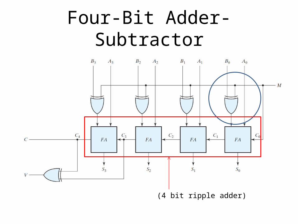
Four-Bit Adder-Subtractor
(4 bit ripple adder)

A Four-Bit Adder/Subtractor on Breadboard
Problem: too many wires!

Add Components


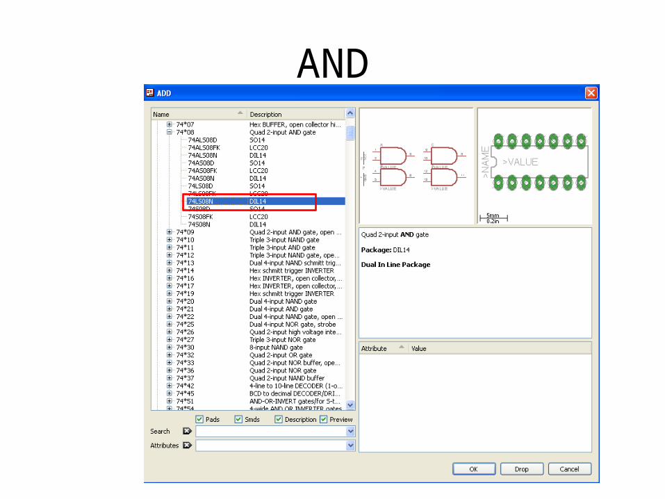
AND

Schematic
Tips
• Double click to terminate a wire

Add Junction to the Schematic
Add junction to the schematic.

Add Power and Gnd of Each IC Chip to the schematic
1. Right click on a part(74LS08N in this example)
2. Click on Invoke
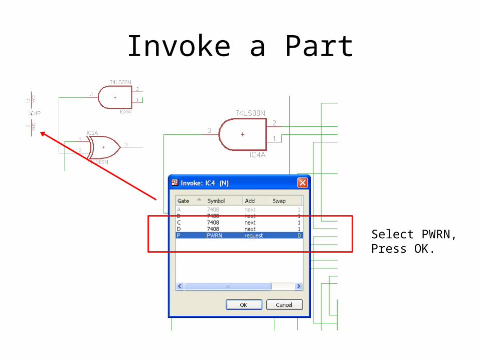
Invoke a Part
Select PWRN, Press OK.

Power and Ground Added

Move• Use the Move button to alter any
component’s location
Click on + to move a part

Delete
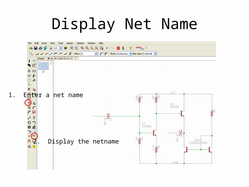
Display Net Name
1. Enter a net name
2. Display the netname

ERC error
Use ERC to check connectivity of the wire.

Rewire to Clear ERC Error
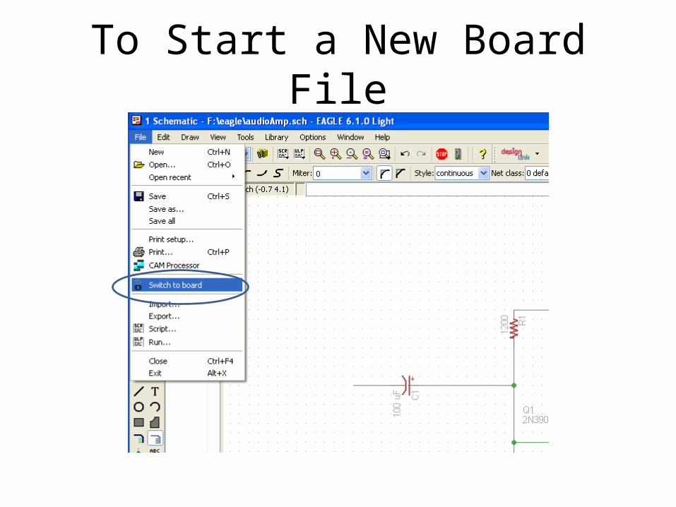
To Start a New Board File

Board Editor
If you keep both windows open, changes made on the schematic windowwill be reflected in the layout window.

Turn on the Grid
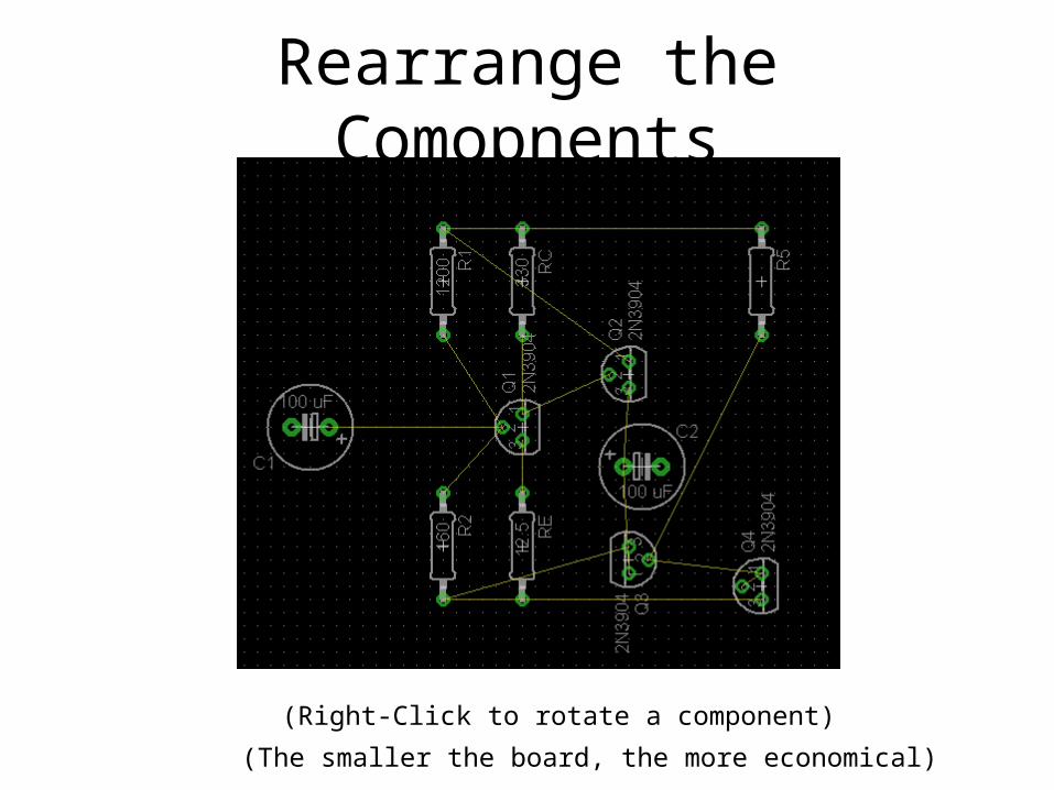
Rearrange the Comopnents
(Right-Click to rotate a component)
(The smaller the board, the more economical)

Click on Route to Start Wiring Up the Circuit
(Left click to selectair wire to route)
Double clickTo remove wire
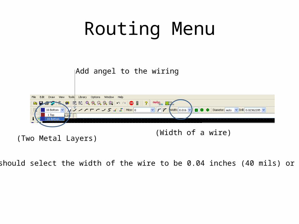
Routing Menu
(Two Metal Layers)(Width of a wire)
You should select the width of the wire to be 0.04 inches (40 mils) or greater.
Add angel to the wiring

Reduce the Active Area
Hieight is 2.5 inches


Load the Design Rules

Minimum Width of 40 miles

Change Clearance Distance

Outer Via Dimensions

Alternative: Load the default autorouter file

Auto Router
Click this optionto start autoroute

Result of Auto Route
2 metal layers usedNot area efficient
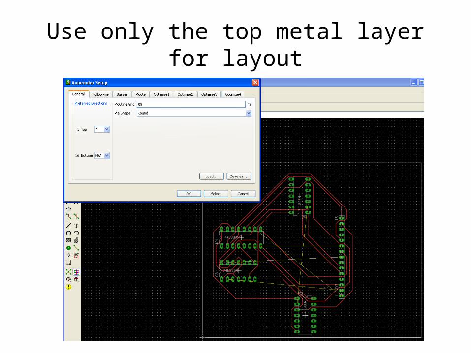
Use only the top metal layer for layout
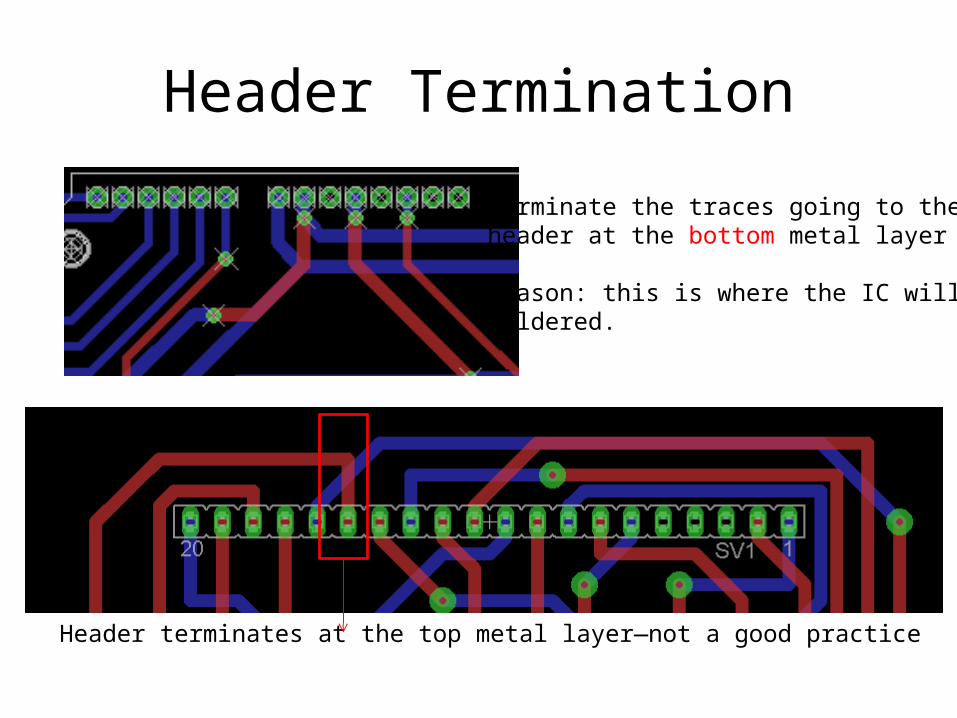
Header Termination
Terminate the traces going to the header at the bottom metal layer
Reason: this is where the IC will besoldered.
Header terminates at the top metal layer—not a good practice

How to Change Metal Layer
Step 1: Click on ripup, double click a wire to delete.

How to Change Metal Layer
Step 2: Move the wires to create sapce

How to Change Metal Layer
Step 3: Route wire. Start routing at the top metal level.Step 4: Click once to place the wire in an empty area.Step 5: Switch to the bottom layerStep 6: Make contact with the pad at the bottom layer

Change the Shape of Via to Round

Round Via

Magnified View
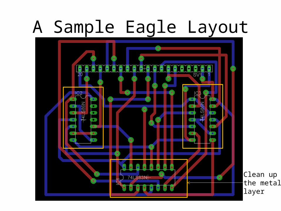
A Sample Eagle Layout
Clean upthe metallayer

Jumpers• You will need to use physical wires as
jumpers in places where you can’t route across existing copper trace.

Add Vias
• Add Vias – Drill 0.03149 (Assumptions: 1. drill bit is
approximately 31 mils in diameter 2. wire size is 29 mils)
– Diameter 0.056 (56 mils)

Provide Connection Via Jumper
(Right click to bend the wire by 45 degrees)
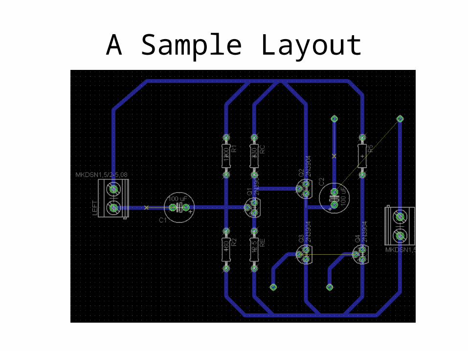
A Sample Layout

Display only the necessary Metal Layers

Print Only Necessary Metal Layers
(Show Bottom trace, pads, and via)

Display top layer
problem

Print Top Layer

Print the Bottom Layer

Print the Layout to a Transparency

Run the transparency through the laser printer twice to produce better transfer
Practice with regularpaper before you use transparency.
Look at your layout on paperand see if it will work at all.
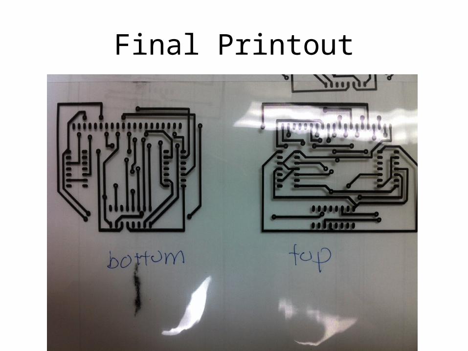
Final Printout
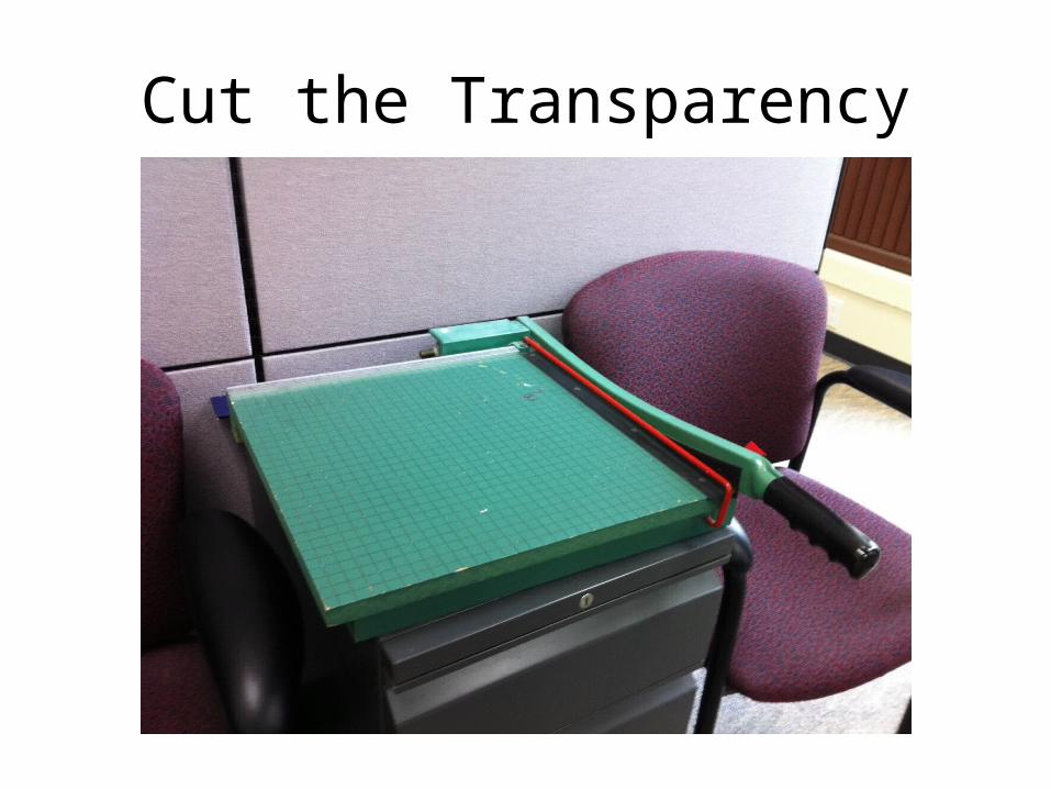
Cut the Transparency

PCB Development
• With contribution from Kevin Zack
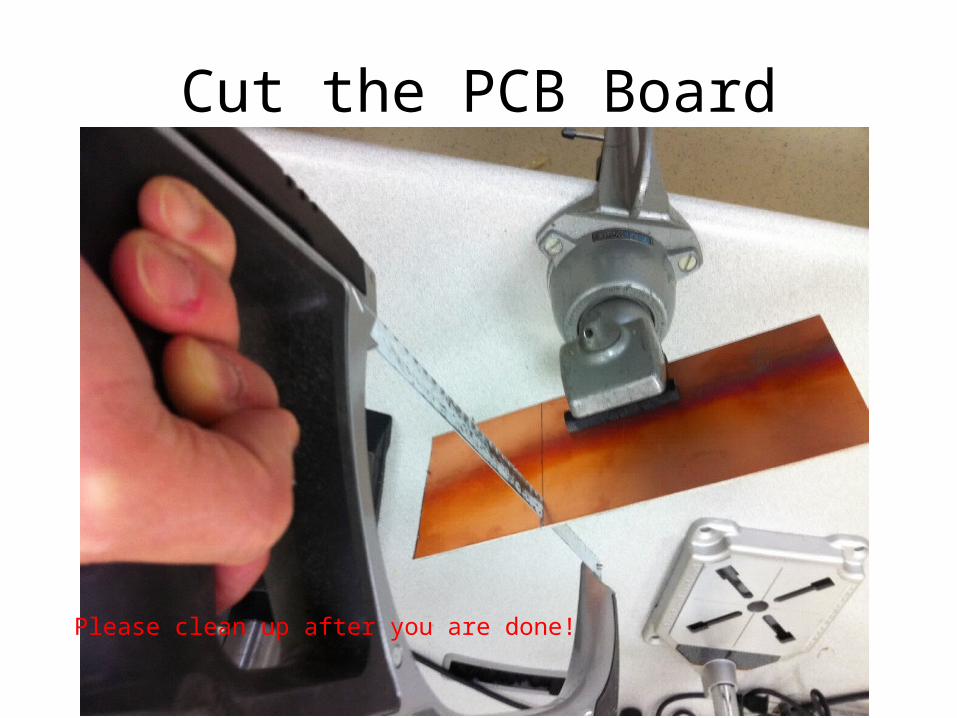
Cut the PCB Board
Please clean up after you are done!

Smooth out the rough edge with Dremel

Clean the PCB with a scotch pad or fine sandpaper

When the board is shiny, use acetone to remove any oil or grease on the board
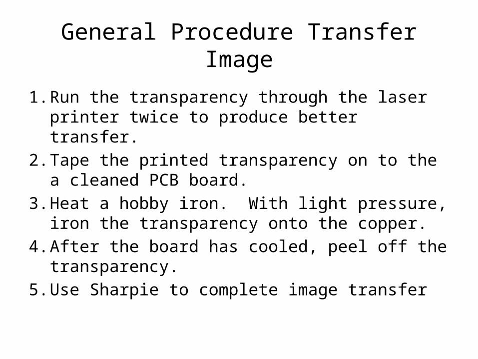
General Procedure Transfer Image
1. Run the transparency through the laser printer twice to produce better transfer.
2. Tape the printed transparency on to the a cleaned PCB board.
3. Heat a hobby iron. With light pressure, iron the transparency onto the copper.
4. After the board has cooled, peel off the transparency.
5. Use Sharpie to complete image transfer
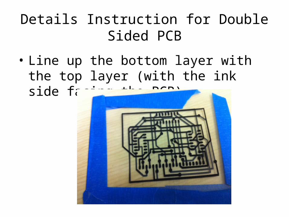
Details Instruction for Double Sided PCB
• Line up the bottom layer with the top layer (with the ink side facing the PCB)
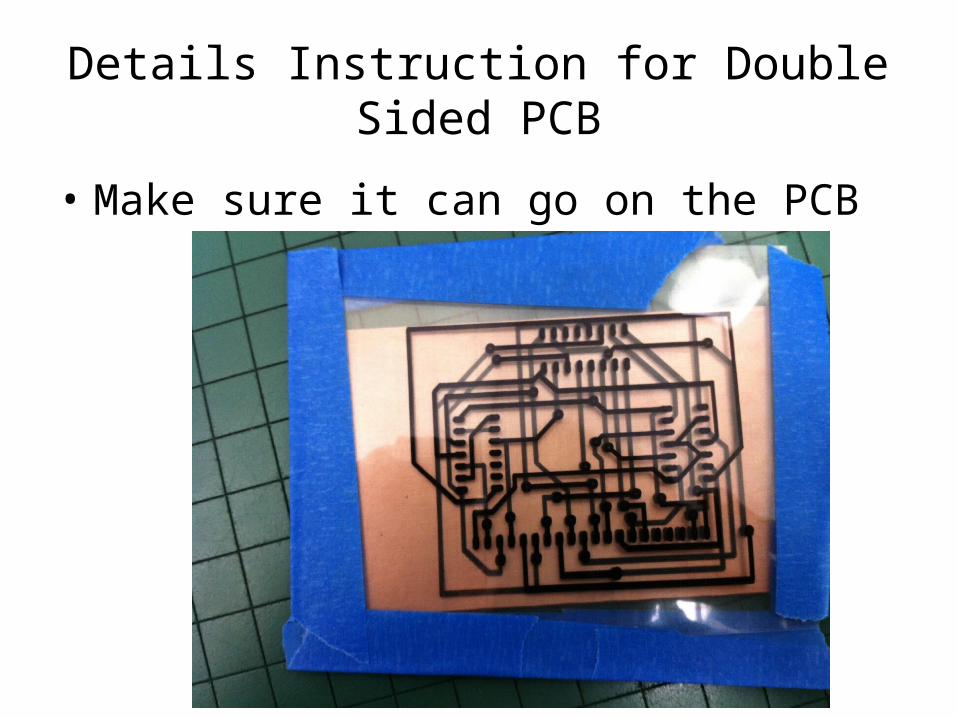
Details Instruction for Double Sided PCB
• Make sure it can go on the PCB
Details Instruction for Double Sided PCB
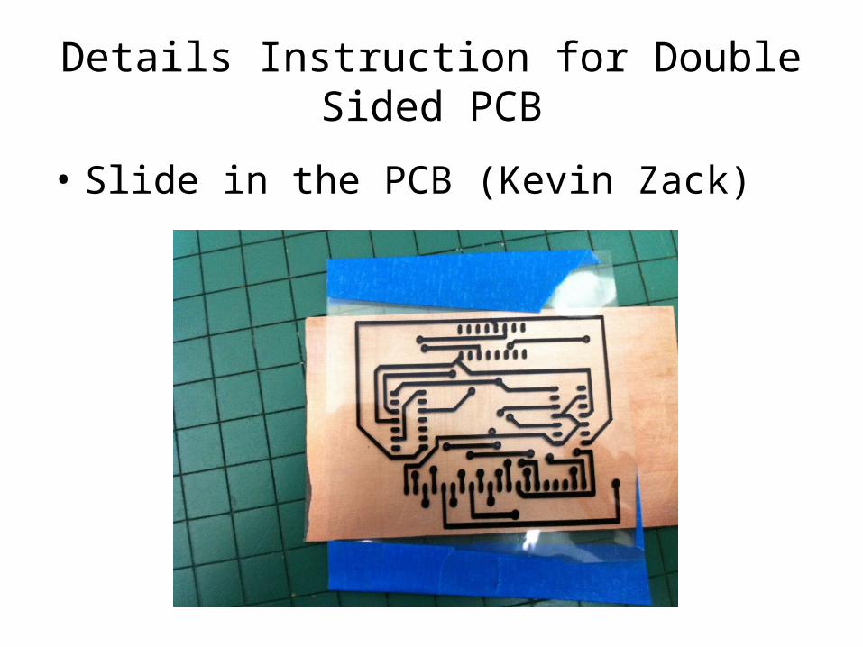
• Slide in the PCB (Kevin Zack)

Details Instruction for Double Sided PCB
• Tape the transparency to PCB
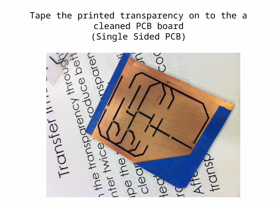
Tape the printed transparency on to the a cleaned PCB board
(Single Sided PCB)
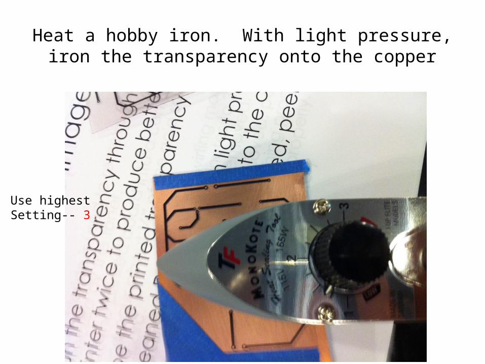
Heat a hobby iron. With light pressure, iron the transparency onto the copper
Use highestSetting-- 3
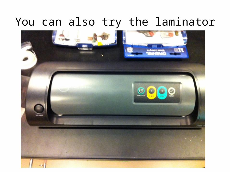
You can also try the laminator

After the board has cooled, peel off the transparency.

Failed Image Transfer

Use Sharpie to Repair PCB Board
Precaution
• Etching Solution may leave stain on skin and utensils. The use of rubber gloves is recommended.
• Avoid prolonged or repeated breathing of vapor or contact with skin.

Develop PCB
1. Ferric Chloride is used to remove the copper not protected by the toner.
2. Place the printed board into a container with a lid and pour about ¼” of the acid solution over the board.
3. Secure the lid and using a swirling motion, agitate the solution for 15 minutes to 30 minutes until the unwanted copper is removed.
4. After the excess copper is removed, pour water over the board to halt the etching process.
5. Dispose the left over chemical properly. (Include the chemical rinsed off with water)
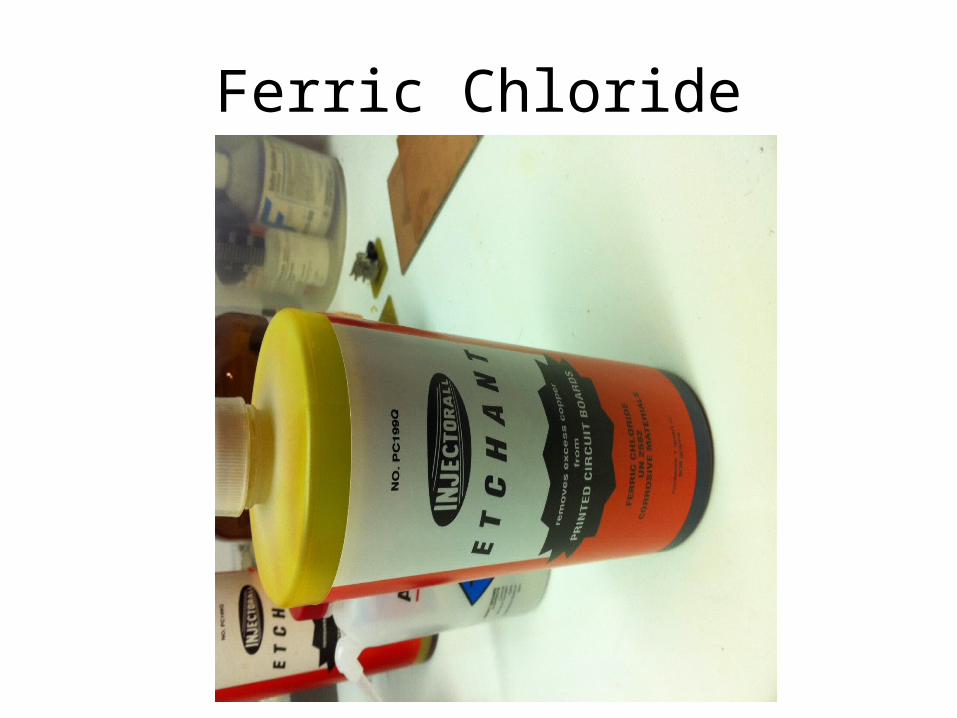
Ferric Chloride

Place the printed board into a container with a lid and pour about ¼” of the acid solution over the board

Agitate the solution

You can also try the orbital shaker
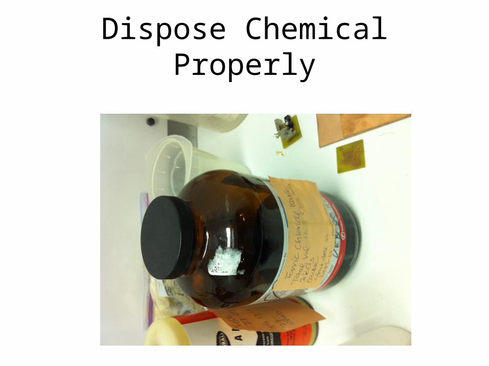
Dispose Chemical Properly
Post Processing
• Clean off the toner protecting the traces with a scotch pad or sandpaper.
• Clean off any residue with acetone.• Drill the board with a drill press. (Use
31 mil drill bit)

Remove Ink
(Before)(After)

Drill Holes

Misc Slides