
processor - MIT CSAIL Parallel and Distributed Operating ... · PDF file1.2.2 Central...
212
Transcript of processor - MIT CSAIL Parallel and Distributed Operating ... · PDF file1.2.2 Central...


processor handbook
digital equipment corporation

Copyright© 1972, by Digital Equipment Corporation
DEC, PDP, UNIBUS are registered trademarks of Digital Equipment Corporation.
ii

TABLE OF CONTENTS
CHAPTER 1 INTRODUCTION
1.1 GENERAL ............................................. .
1.2 GENERAL CHARACTERISTICS . 1.2.1 The UNIBUS ..... 1.2.2 Central Processor 1.2.3 Memories ........... . 1.2.4 Floating Point ... . 1.2.5 Memory Management .............................. ..
1·1
1·1
1·2 1·2 1·3 1·5 1·5 1·5
1.3 PERIPHERALS/OPTIONS ......................................... 1·5 1.3.1 1/0 Devices .......... .................................. 1·6 1.3.2 Storage Devices ...................................... .. 1.3.3 Bus Options .............................................. .
1·6 1·6
1.4 SOFTWARE ..... .... ........................................... ............. 1·6 1.4.1 Paper Tape Software .......................................... 1·7 1.4.2 Disk Operating System Software ........................ 1·7 1.4.3 Higher Level Languages ................................... .. 1·7
1.5 NUMBER SYSTEMS ..................................... . 1-7
CHAPTER 2 SYSTEM ARCHITECTURE.
2.1 2.2
2.3
2.4 2.5 2.6
2.7
SYSTEM DEFINITION .............. . UNIBUS ......................................... . 2.2.1 Bidirectional Lines ...... . 2.2.2 Master-Slave Relation .. 2.2.3 Interlocked Communication CENTRAL PROCESSOR .......... . 2.3.1 General Registers ... . 2.3.2 Processor Status Word ....... . 2.3.3 Stack Limit Register EXTENDED INSTRUCTION SET & FLOATING POINT .. CORE MEMORY . . . .... AUTOMATIC PRIORITY INTERRUPTS .... 2.6.1 Using the Interrupts . 2.6.2 Interrupt Procedure 2.6.3 Interrupt Servicing ............ .. PROCESSOR TRAPS ............ . 2.7.1 Power Failure ............... . 2.7.2 Odd Addressing Errors ... . ......... . 2.7.3 Time-out Errors ...... . 2.7.4 Reserved Instructions 2.7.5 Trap Handling ........... .
iii
2-1
2·1 2-1 2-1 2-2 2-2 2-2 2-3 2-4 2-5 2-5 2-6 2-7 2-9 2-9 2-10 2-10 2-10 2-10 2·11 2-11 2-11
CHAPTER 3 ADDRESSING MODES .............................................. 3·1
3.1 SINGLE OPERAND ADDRESSING ...................... ......... 3·2 3.2 DOUBLE OPERAND ADDRESSING ................................ ~-2 3.3 DIRECT ADDRESSING .. . .. .. .. .. . . . . .. . .. ... .. . . .. . .. . .. . ... .. ... ... ... 3-4
3.3.1 Register Mode .................................................. 3·4 3.3.2 Auto-increment Mode . . . . . . . . . .. .. . . . . .. . . .. . .. . .. .. . . .. . . . . . 3·5 3.3.3 Auto-decrement Mode ...................................... 3·7 3.3.4 Index Mode . . . . . . . . . . . . . . . . . . . . . . . . . . . . . . . . . . . . . . . . . . . . . . . . . . . .. . .. 3·8
3.4 DEFERRED (INDIRECT) ADDRESSING ......................... 3·10 3.5 USE OF THE PC AS A GENERAL REGISTER ................ 3·12
3.5.1 Immediate Mode................................................ 3·13 3.5.2 Absolute Addressing .. ......... ............................... 3·13 3.5.3 Relative Addressing ....... .................................. 3·14 3.5.4 Relative Deferred Addressing .. . .. . . . . . . . .. . .. . . . . .. .. . .. 3·15
3.6 USE OF STACK POINTER AS GENERAL REGISTER ...... 3·16 3.7 SUMMARY OF ADDRESSING MODES .......................... 3·16
3.7.1 General· Register Addressing ............................ 3·16 3.7.2 Program Counter Addressing ............................ 3·18
CHAPTER 4 INSTRUCTION SET . . . . . . . . . . . . . . . . . . . . . . . . . . . . . . . . . . . . . . . . . . . . . . . . . . 4·1
4.1 INTRODUCTION ............................................................ 4·1 4.2 INSTRUCTION FORMATS .. .. ...... ... ................................ 4·2 4.3 LIST OF INSTRUCTIONS . . . .. . . . . .. . . . . .. . . . . .. . . . . . . .. . .. . . . . .. . . . . .. 4·4 4.4 SINGLE OPERAND INSTRUCTIONS . . . .. . . . . .. .. . . . . . . . . .. . . .. .. . .4·6 4.5 .DOUBLE OPERAND INSTRUCTIONS ............... .. ....... .... 4·22 4.6· PROGRAM CONTROL INSTRUCTIONS ..... ............ ......... 4·36 4.7 MISCELLANEOUS ..... ..................................................... 4·74
CHAPTER 5 PROGRAMMING TECHNIQUES ................................ 5·1
5.1 THE STACK .................................................................. 5·1 5.2 SUBROUTINE LINKAGE ................................. ............... 5·5
5.2.1 Subroutine Calls .... ........................................... 5·5 5.2.2 Argument Transmission . . . .. . . . . .. . . .. .. . . .. . .. . .. .. . ... .. . 5·6 5.2.3 Subroutine Return . . . . . . . . . . . . . . . . . . . . . . . . . . . . . . . . . . . . . . . .. . . . 5·9 5.2.4 PDP·ll Subroutine Advantage .......................... 5·9
5.3 INTERRUPTS . . ... ... . .... .. .. .. . ... . .. . .. .. .. .. . . . ... . . . . .. .. . ....... .. . ... . 5·9 5.3.1 General Principles ............................................ 5·9 5.3.2 Nesting ..... .................. ....................................... 5·10
5.4 REENTRANCY ................................................................ 5·13 5.5 POSITION INDEPENDENT CODE .................................. 5·15 5.6 CO· ROUTINES ........... .......... ........... ................................ 5·16 5.7 MULTI-PROGRAMMING ................................................ 5·17
5.7.1 Control Information .......................................... 5·17 5.7.2 Data .................................................................. 5·17 5.7.3 Processor Status Word ...................................... 5·17
iv

CHAPTER 6 MEMORY MANAGEMENT
6.1 PDP-11 FAMILY BASIC ADDRESSING LOGIC ............... 6-1 6.2 VIRTUAL ADDRESSING .... ...................... 6-2 6.3 INTERRUPT CONDITIONS UNDER MANAGEMENT
CONTROL....................................................................... 6-2 6.4 CONSTRUCTION OF A PHYSICAL ADDRESS ............... 6-3 6.5 MANAGEMENT REGISTERS ........................................... 6-4
6.5.1 Page Address Register...................................... 6-5 6.5.2 Page Descriptor Register ........ ........................... 6-5
6.6 FAULT REGISTERS .. ............................. ...................... 6-7 6.6.1 Status Register #0 ........................................... 6-7 6.6.2 Status Register #2 ........................................... 6-8
CHAPTER 7 INTERNAL PROCESSOR OPTIONS
7.1 GENERAL ....................................................................... 7-1 7.2 EIS OPTION ................................................................... 7-1 7.3 FLOATING POINT OPTION ............................................. 7-3 7.4 STACK LIMIT OPTION ....... ........................................... 7-5
CHAPTER 8 CONSOLE OPERATION
8.1 CONSOLE ELEMENTS ................. ................................. 8-1 8.2 STATUS INDICATORS ................................................... 8·2 8.3 CONSOLE SWITCHES.................................................... 8-3 8.4 DISPLAYS....................................................................... 8-4
CHAPTER 9 SPECIFICATIONS
9.1 PACKAGING ................................................................... 9-1 9.2 CPU OPERATING SPECIFICATIONS ............................... 9-1 9.3 OTHER EQUIPMENT ..................................................... 9-1 9.4 PDP-11 FAMILY OF COMPUTERS ................................. 9-4
Appendix A Instruction Set Processor ........................................ A-1
Appendix B Memory Map ............................................................ 8·1
Appendix C PDP-11/40 Instruction Timing .................................. C-1
Appendix D Instruction Index and Numerical Op Code List ........ D-1
Appendix E Summary of PDP11 Instructions .............................. E-1
v

vi

CHAPTER 1
INTRODUCTION
1.1 GENERAL The PDP-11 family includes several central processors, a large number of peripheral devices and options, and extensive software. PDP-11 com· puters have similar architecture and are hardware and software upwards compatible, although each machine has some of its own characteristics. New systems will be compatible with existing family members. The user can choose the system which is most suitable for his application, but as needs change or grow he can easi!y add or change hardware.
This Handbook describes the PDP-11/40, one of the latest computers in the PDP-11 family from Digital Equipment Corporation (DEC). This powerful, low-priced machine is packaged in a 21·'' front panel slide chassis, allowing convenient access and expansion when mounted in a standard rack. The PDP-11/40 was designed to fit a broad range of applications, from small stand alone situations where the computer consists of only 8K of memory and a processor, to large multi-user, multitask applications requiring up to 124K of addressable memory space. Among its major features are a fast central processor with a choice of floating point and sophisticated memory management, both of which are hardware options.
Some of the PDP-11/40 features are: • 16-bit word (two 8-bit bytes)
direct addressing of 32K 16-bit words or 64K 8-bit bytes (K = 1024) • Word or byte processing
very efficient handling of 8-bit characters • Asynchronous operation
systems run at their highest possible speed, replacement with faster devices means faster operation with no other hardware or software changes
• Modular component design extreme ease and flexibility in configuring systems
• Stack Processing hardware sequential memory manipulation makes it easy to handle structured data, subroutines, and interrupts
1·1

• 8 fast general-purpose registers very fast integrated circuits used in tera:tively for instruction processing
• Automatic priority processing four-line, multi-level system is dynamically alterable
• Vectored interrupts fast interrupt response without device polling
• Single & double operand instructions powerful and convenient set of micro-programmed instructions
DEC References The following publications contain supplementary and useful information:
Title
PDP-11 Peripherals and Interfacing Handbook
PDP-11 UNIBUS Interface Manual
Introduction to Programming
Small Computer Handbook
1.2 GENERAL CHARACTERISTICS 1.2.1 The UNIBUS All computer system components and peripherals connect to and communicate with each other on a single high-speed bus known as the UNIBU5-the key to the PDP-11's many strengths. Since all system elements, including the central processor, communicate with each other in identical fashion via the UNIBUS, the processor has the same easy access to peripherals as it has to memory.
Figure 1-1 PDP-11 System Simplified Block Diagram
With bidirectional and asynchronous communications on the UNIBUS, devices can send, receive, and exchange data independently without processor intervention. For example, a cathode ray tube (CRT) display can refresh itself from a disk file while the central processor unit (CPU) attends to other tasks. Because it is asynchronous, the UNIBUS is compatible with devices operating over a wide range of speeds.
Device communications on the UNIBUS are interlocked. For each command issued by a "master" device, a response signal is received from a
1-2

"slave" completing the data transfer. Device·to·device communication is completely independent of physical bus length and the response times of master and slave devices.
Interfaces to the UNIBUS are not time-dependent; there are no pulse· width or rise-time restrictions to worry about. The maximum transfer rate on the UNIBUS is one 16·bit word every 400 nanoseconds, or 2,500,000 words per second.
Input/output devices transferring directly to or from memory are given highest priority and may request bus mastership and steal bus and mem· ory cycles during instruction operations. The processor resumes opera· tion immediately after the memory transfer. Multiple devices can operate simultaneously at maximum direct memory access (DMA) rates by "stealing" bus cycles.
1.2.2 Central Processor The central processor, connected to the UNIBUS as a subsystem, con· trois the time allocation of the UNIBUS for peripherals and performs arithmetic and logic operations and instruction decoding. It contains multiple high-speed general-purpose registers which can be used as accu· mulators, address pointers, index registers, and other specialized func· tions. The processor can perform data transfers directly between 1/0 devices and memory without disturbing the processor registers; does both single· and double-operand addressing and handles both 16-bit word and S·bit byte data.
Instruction Set The instruction complement uses the flexibility of the general-purpose registers to provide over 400 powerful hard-wired instructions-the most comprehensive and powerful instruction repertoire of any computer in the 16-bit class. Unlike conventional 16-bit computers, which usually have three classes of instructions (memory reference instructions, oper· ate or AC control instructions and 1/0 instructions) all operations in the PDP·ll are accomplished with one set of instructions. Since peripheral device registers can be manipulated as flexibly as core memory by the central processor, instructions that are used to manipulate data in core memory may be used equally well for data in peripheral device registers. For example, data in an external device register can be tested or modified directly by the CPU, without bringing it into memory or disturbing the general registers. One can add data directly to a peripheral device reg· ister, or compare logically or arithmetically contents with a mask and branch. Thus all PDP·ll instructions can be used to create a new dimen· sion in the treatment of computer 1/0 and the need for a special class of 1/0 instructions is eliminated.
The basic order code of the PDP·ll uses both single and double operand address instructions for words or bytes. The PDP·ll therefore performs very efficiently in one step, such operations as adding or subtracting two operands, or moving an operand from one location to another.
ADD A,B
PDP·ll Approach
;add contents of location A to location B, store result at location B
1·3

LOA A
ADD B
STAB
Priority Interrupts
Conventional Approach
;load contents of memory location A into AC
;add contents of memory location B to AC
;store result at location B
A multi-level automatic priority interrupt system permits the processor to respond automatically to conditions outside the system. Any number of separate devices can be attached to each level.
Each peripheral device in the PDP-11 system has a hardware pointer to its own pair of memory words (one points to the devices's service routine, and the other contains the new processor status information}. This unique identification eliminates the need for polling of devices to identify an interrupt, since the interrupt servicing hardware selects and begins executing the appropriate service routine after having automatically saved the status of the interrupted program segment.
The devices' interrupt priority and service routine priority are independent. This allows adjustment of system behavior in response to_ real-time conditions, by dynamically changing the priority level of the service routine.
The interrupt system allows the processor to continually compare its own programmable priority with the priority of any interrupting devices and to acknowledge the device with the highest level above the processors priority level. Servicing an interrupt for a device can be interrupted for servicing a higher priority device. Service to the lower priority device is resumed automatically upon completion of the higher level servicing. Such a process, called nested interrupt servicing, can be carried out to any level without requiring the software to save and restore processor status at each level.
Reentrant Code Both the interrupt handling hardware and the subroutine call hardware facilitate writing reentrant code for the PDP-11. This type of code allows a single copy of a given subroutine or program to be shared by more than one process or task. This reduces the amount of core needed for multi-task applications such as the concurrent servicing of many peripheral devices.
Addressing Much of the power of the PDP-11 is derived from its wide range of addressing capabilities. PDP-11 addressing modes include sequential addressing forwards or backwards, address indexing, indirect addressing, 16-bit word addressing, 8-bit byte addressing, and stack addressing. Variable length instruction formating allows a minimum number of bits to be used for each addressing mode. This results in efficient use of program storage space.
1-4

Stacks In the PDP·ll, a stack is a temporary data storage area which allows a program to make efficient use of frequently accessed data. The stack is used automatically by program interrupts, subroutine calls, and trap in· structions. When the processor is interrupted, the central processor status word and the program counter are saved (pushed) onto the stack area, while the processor services the interrupting device. A new status word is then automatically acquired from an area in core memory which is reserved for interrupt instructions (vector area). A return from the interrupt instruction restores the original processor status and returns to the interrupted program without software intervention.
Direct Memory Access All PDP·ll's provide for direct access to memory. Any number of DMA devices may be attached to the UNIBUS. Maximum priority is given to DMA devices thus allowing memory data storage or retrieval' at memory cycle speeds. Latency is minimized by the organization and logic of the UNIBUS, which samples requests and priorities in parallel with data transfers.
Power Fail and Restart The PDP·ll's power fail and restart system not only protects memory when power fails, but also allows the user to save the existing program location and status (including all dynamic registers), thus preventing harm to devices, and eliminating the need for reloading programs. Auto· matic restart is accomplished when power returns to safe operating levels, enabling remote or unattended operations of PDP·ll systems. All standard peripherals in the PDP·ll family are included in the systemized power-fail protect/ restart feature.
1.2.3 Memories Memories with different ranges of speeds and various characteristics can be freely mixed and interchanged in a single PDP·ll system. Thus as memory needs expand and as memory technology grows, a PDP·ll can evolve with none of the growing pains and obsolescence associated with conventional computers.
1.2.4 Floating Point (optional) A Floating Point Unit functions as an integral part of the PDP·ll/40 processor, not as a bus device.
1.2.5 Memory Management (optional) PDP·ll/40 Memory Management is an advanced memory extension, relocation, and protection feature which will:
extend memory space from 28K to 124K words allow efficient segmentation of core for multi-user environments provide effective protection of memory segments in multi-user en· vironments
1.3 Peripherals/Options Digital Equipment Corporation (DEC) designs and manufactures many of the peripheral devices offered with PDP·ll's. As a designer and manu·
1·5

facturer of peripherals, DEC can offer extremely reliable equipment, lower prices, more choice and quantity discounts.
1.3.1 1/0 Devices All PDP·ll systems are available with Teletypes as standard equipment. However, their 1/0 capabilities can be increased with high speed paper tape reader-punches, line printers, card readers or alphanumeric display terminals. The LA30 DECwriter, a totally DEC·designed and built tele· printer, can serve as an alternative to the Teletype. It has several ad· vantages over standard electromechanical typewriter terminals, including higher speed, fewer mechanical parts and very quiet operation.
PDP·ll 1/0 devices include:
DECterminal alphanumeric display DECwriter teleprinter High Speed Line Printers High Speed Paper Tape Reader and Punch Teletypes Card Readers Synchronous and Asynchronous Communications Interfaces
1.3.2 Storage Devices Storage devices range from convenient, small·reel magnetic tape (DEC· tape) units to mass storage magnetic tapes and disk memories. With the UNIBUS, a large number of storage devices, in any combination, may be connected to a PDP·ll system. TU56 DECtapes, highly reliable tape units with small tape reels, designed and built by DEC, are ideal for applica· tions with modest storage requirements. Each DECtape provides storage for 144K 16-bit words. For applications which require handling of large volumes of data, DEC offers the industry compatible TU10 Magtape.
Disk storage include fixed-head disk units and moving-head removable cartridge and disk pack units. These devices range from the 64K RS64 DECdisk memory, to the RP02 Disk Pack system which can store up to 93.6 million words.
PDP·ll storage devices include:
DECtape Magtape RS64 64K-256K word fixed-head disk RSll 256K·2M word fixed-head disk RK05 1-2M word moving-head disk RP02 10M word moving-head disk
1.3.3 Bus Options Several options (bus switches, bus extenders) are available for extending the UNIBUS or for configuring multi-processor or shared-peripheral systems.
1.4 SOFTWARE Extensive software, consisting of disk and paper tape systems, is avail·
1·6

able for PDP-11 Family systems. The larger the PDP-11 configuration, the larger and more comprehensive the software package that comes with it.
1.4.1 Paper Tape Software The Paper Tape Software system includes:
Editor (ED11) Assembler (PALll) Loaders On-line Debugging Technique (ODT11) Input-Output Executive (lOX) Math Package (FPPll)
1.4.2 Disk Operating System Software The Disk Operating System software includes:
Text Editor (ED11) MACRO Assembler (MACR0·11) Linker (LINK11) File Utilities Packages (PIP) On Line Debugging Technique (ODTll) Librarian (LIBR11)
1.4.3 Higher Level Languages PDP-11 users needing an interactive conversational language can use BASIC which can be run on the paper tape software system with only 4,096 words of core memory. A multi-user extension of BASIC is avail· able so up to eight users can access a PDP-11 with only SK of core.
BATCH The BATCH System adds job stream processing to the DOS System.
RST5-11 The PDP-11 Resource Timesharing System (RSTS-11) with BASIC-PLUS, an enriched version of BASIC, is available for up to 16 terminal users.
FORTRAN PDP-11 FORTRAN is an ANSI-standard FORTRAN IV compiler.
1.5 NUMBER SYSTEMS Throughout this Handbook, 3 number systems will be used; octal, binary, and decimal. So as not to clutter all numbers with subscripted bases, the following general convention will be used:
Octal-for address locations, contents of addresses, and operation codes for instructions; in most cases there will be words of 6 octal digits
Binary-for describing a single binary element; when referring to a PDP-11 word it will be 16 bits long
Decimal-for all normal referencing to quantities
1-7

Octal Representation
:-:--1~5114 13 12l11 10 gl e 1 &15 4 3 [ 2 1 o I PDP-11 word
~~-------_!---)~~ I I ~~---------~ D D D D D D 6-digit octal
The 16-bit PDP-11 word can be represented conveniently as a 6-digit octal word. Bit 15, the Most Significant Bit (MSB), is used directly as the MSB of the octal word. The other 5 octal digits are formed from the corresponding groups of 3 bits in the binary word.
When an extended address of 18 bits is used (shown later in the Handbook), the MSB of the octal word is formed from bits 17, 16, and 15. For unsigned numbers, the correspondence between decimal and octal is:
Decimal
0 (216-1)= 65,535 (218-1)=262,143
2's Complement Numbers
Octal
000000 177777 777777
(16-bit limit) (18-bit limit)
In this system, the first bit (bit 15) is used to indicate the sign;
O=positive 1=negative
For positive numbers, the other 15 bits represent the magnitude directly; for negative numbers, the magnitude is the 2's complement of the remaining 15 bits. (The 2's complement is equal tp the 1's complement plus one.) The ordering of numbers is shown below:
Decimal 2's Complement (Octal)
Sign Bit Magnitude Bits largest positive +32,767 0 77777
+32,766 0 77776
+1 0 00001 0 0 00000
-1 1 77777 -2 1 77776
-32,767 1 00001 most negative -32,768 1 00000
1-8

CHAPTER 2
SYSTEM ARCHITECTURE
2.1 SYSTEM DEFINITION
The PDP-11/40 is a 16-bit, general-purpose, parallel logic computer using 2's complement arithmetic. The processor can directly address 32,768 16-bit words or 65,536 8-bit bytes.
The Central Processing Unit performs all arithmetic and logical operations required in the system. A Floating Point Unit mounts integrally into the Central Processor as does a Memory Management Unit which provides a full memory managemnt facility through relocation and protection.
The PDP-11/40 hardware has been optimized towards a multi-programming environment and the processor therefore operates in two modes (Kernel and User). By taking full advantage of this feature, a software operating system can insure that no user (who is operating in User mode) can cause a failure (crash) of the entire system. Full control of the entire system is retained at the console or by an operator who is in Kernel mode.
2.2 UNIBUS The UNIBUS is a single, common path that connects the central processor, memory, and all peripherals. Addresses, data, and control information are sent along the 56 lines of the bus.
The form of communication is the same for every device on the UNIBUS. The processor uses the same set of signals to communicate with memory as with peripheral devices. Peripheral devices also use this set of signals when communicating with the processor, memory or other peripheral devices. Each device, including memory locations, processor registers, and peripheral device registers, is assigned an address on the UNIBUS. Thus, peripheral device registers may be manipulated as flexibly as core memory by the central processor. All the instructions that can be applied to data in core memory can be applied equally well to data in peripheral device registers. This is an especially powerful feature, considering the special capability of PDP-11 instructions to process data in any memory location as though it were an accumulator.
2.2.1 Bidirectional Lines Most UNIBUS lines are bidirectional, so that the same signals that are received as input can be driven as output. This means that a peripheral device register can be either read or loaded by the central processor or
2-1

other peripheral devices; thus, the same register can be used for both input and output functions.
2.2.2 Master-Slave Relation Communication between two devices on the bus is in the form of a master-slave relationship. At any point in time, there is one device that has control of the bus. This controlling device is termed the "bus mas· ter". The master device controls the bus when communicating with another device on the bus, termed the "slave". A typical example of this relationship is the processor, as master, fetching an instruction from memory (which is always a slave). Another example is the disk, as master, transferring data to memory, as slave. Master-slave relation· ships are dynamic. The processor, for example, may pass bus control to a disk. The disk, as master, could then communicate with a slave memory bank.
Since the UNIBUS is used by the processor and all 1/0 devices, there is a priority structure to determine which device gets control of the bus. Every device on the UNIBUS which is capable of becoming bus master is assigned a priority. When two devices, which are capable of becoming a bus master, request use of the bus simultaneously, the device with the higher priority will receive control.
2.2.3 Interlocked Communication Communication on the UNIBUS is interlocked so that for each control signal issued by the master device, there must be a response from the slave in order to complete the transfer. Therefore, communication is independent of the physical bus length (as far as timing is concerned) and the response time of the master and slave devices. This asynchron· ous operation precludes the need for synchronizing with, and waiting for, clock pulses. Thus, each device is allowed to operate at its maximum possible speed.
2.3 CENTRAL PROCESSOR The PDP·ll/40 performs all arithmetic and logical operations required in the system. It also acts as the arbitration unit for UNIBUS control by regulating bus requests and transferring control of the bus to the re· questing device with the highest priority.
Space is provided within the central processor for the following options:
Extended Instruction Set Floating Point Unit Memory Management Unit Programmable Stack Limit
The machine operates in two modes; Kernel and User. When the machine is in Kernel mode a program has complete control of the machine; when in User mode the processor is inhibited from executing certain instructions and can be denied direct access to the peripherals on the system. This hardware feature can be used to provide complete execu· tive protection in a multi-programming environment.
The central processor contains 8 general registers which can be used as accumulators, index registers, or as stack pointers. A stack, as used
2·2

in the PDP-11, is an area of memory set aside by the programmer for temporary storage or subroutine/ interrupt service linkage. A program can add or delete words or bytes within the stack. The stack uses che "lastin, first-out" concept; that is, various items may be added to a stack in sequential order and retrieved or deleted from the stack in reverse order. On the PDP-11, a stack starts at the highest location reserved for it and expands linearly downward to the lowest address as items are added. Stacks are extremely useful for nesting programs, creating reentrant coding, and as temporary storage where a Last-In, First-Out structure is desirable. One of the general registers is used as the PDP-11 I 40's Program Counter. Two others are used as Processor Stack Pointers, one for each operational mode.
The CPU performs all of the computer's computation and logic operations in a parallel binary mode through step by step execution of individual instructions.
2.3.1 General Registers The general registers can be used for a variety of purposes; the uses varying with requirements. The general registers can be used as accumulators, index registers, autoincrement registers, autodecrement registers, or as stack pointers for temporary storage of data. Chapter 3 on Addressing describes these uses of the general registers in more detail. Arithmetic operations can be from one general register to another, from one memory or device register to another, or between memory or a device register and a general register.
GENERAL REGISlERS R0
R1
R2
R3
R4
R5
R6
KERNEL STACK POINTER
R7
PROGRAM COUNTER
l<sPl R6
USER STACK POINTER
(WITH MEMORY
I<PCl MANAGEMENT OPTION)
Figure 2-1 The General Registers
R7 is used as the machine's program counter (PC) and contains the address of the next instruction to be executed. It is a general register
2-3
normally used only for addressing purposes and not as an accumulator for arithmetic operations.
The R6 register is normally used as the Processor Stack Pointer indicat· ing the last entry in the appropriate stack (a common temporary storage area with "Last-in First-Out" characteristics). The two stacks (with the Memory Management option) are called the Kernel Stack and the User Stack. When the Central Processor is operating in Kernel mode it uses the Kernel Stack and in User mode, the User Stack. When an interrupt or trap occurs, the PDP·ll/40 automatically saves its current status on the Processor Stack selected by the service routine. This stack·based architecture facilitates reentrant programming.
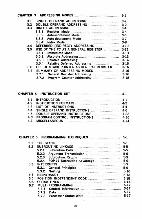
2.3.2 Processor Status Word
15 14131211 87 54
CURRENT M~t ..______.._.,} PREVIOUS MOOE"t'-----'PRIORITY--------------_J CONDITION CODES
*MODE: 00•KERNEL II =USER
Figure 2-2 Processor Status Word
3 2 I 0
T The Processor Status Word (PS), located at location 777776, contains information on the current status of the PDP-11/40. This information includes the current processor priority: current and previous operational modes; the condition codes describing the results of the last instruction; and an indicator for detecting the execution of an instruction to be trapped during program debugging.
Modes (with Memory Management Option) Mode information includes the present mode, either User or Kernel (bits 15, 14) and the mode the machine was in prior to the last interrupt or trap (bits 13, 12).
The two modes permit a fully protected environment for a multiprogramming system by providing the user with two distinct sets of Processor Stacks and Memory Management Registers for memory mapping. In User mode a program is inhibited from executing a "HALT" instruction and the processor will trap through location 10 if an attempt is made to execute this instruction. Furthermore, the processor will ignore the "RESET" instruction. In Kernel mode, the processor will execute all instructions.
A program operating in Kernel mode can map users' programs anywhere in core and thus explicitly protect key areas (including the device registers and the Processor Status Word) from the User operating environment.
2-4

Processor Priority The Central Processor operates at any one of eight levels of priority, 0·7. When the CPU is operating at level 7 an external device cannot interrupt it with a request for service. The Central Processor must be operating at a lower priority than the external device's request in order for the interruption to take effect. The current priority is maintained in the processor status word (bits 5·7). The 8 processor levels provide an ef· fective interrupt mask.
Condition Codes The condition codes contain information on the result of the last CPU operation.
The bits are set as follows:
Z = 1, if the result was zero N = 1, if the result was negative C = 1, if the operation resulted in a carry from the MSB V = 1, if the operation resulted in an· arithmetic overflow
Trap The trap bit (T) can be set or cleared under program control. When set, a processor trap will occur through location 14 on completion of instruction execution and a new Processor Status Word will be loaded. This bit is especially useful for debugging programs as it provides an efficient method of installing breakpoints.
Interrupts and trap instructions both automatically cause the previous Processor Status Word and Program Counter to be saved and replaced by the riew values corresponding to those required by the routine ser· vicing the interrupt or trap. The user can, thus, cause the central proces· sor to automatically switch modes, or disable the Trap Bit whenever a trap or interrupt occurs.
2.3.3 Stack Register (with Memory Management option) All PDP·ll's have a Stack Overflow Boundary at location 400,. The Ker· nel Stack Boundary, in the PDP-11/40 is a variable boundary set through the Stack Limit Register found at location 777774.
Once the Kernel stack exceeds its boundary, the Processor will complete the current instruction and then trap to location 4 (Yellow or Warning Stack Violation). If, for some reason, the program persists beyond the 16-word limit, the processor will abort the offending instruction, set the stack point (R6) to 4 and trap to location 4 (Red or Fatal Stack Viola· tion).
2.4 EXTENDED INSTRUCTION SET & FLOATING POINT The Extended Instruction Set (EIS) option fits within the Central Pro· cessor mounting assembly. It provides the capability of performing hard· ware fixed point arithmetic and allows direct implementation of multiply, divide, and multiple shifting. A double-precision 32-bit word can be handled.
The Floating Point Unit, which uses the EIS as a prerequisite, fits within the CPU mounting assembly. This option enables the execution of 4
2·5

special instructions for floating point addition, subtraction, multiplication, and division. The EI.S and Floating Point hardware provide significant time and coding improvement over comparable software routines.
2.5 CORE MEMORY Memory Organization A memory can be viewed as a series of locations, with a number (address) assigned to each location. Thus a 4096-word PDP-11 memory could be shown as in Figure 2-3.
OCTAl. AOORESSES
000000
000001
000002
000003
000004
017774
017775
017776
017777
l.OCATIONS
........ -~
Figure 2-3 Memory Addresses
Because PDP-11 memories are designed to accommodate both 16-bit words and 8-bit bytes, the total number of addresses does not correspond to the number of words. A 4096-word memory can contain 8,192 bytes and consists of 017777 octal locations. Words always start at evennumbered locations.
A PDP-11 word is divided into a high byte and a low byte as shown in Figure 2-4.
15
HIGH BYTE 1 I
B 7
LOW BYTE
Figure 2-4 High & Low Byte
0
Low bytes are stored at even-numbered memory locations and high bytes at odd-numbered memory locations. Thus it is convenient to view the PDP-11 memory as shown in Figure 2-5.
2-6
000001
000003
000005
I
-
BYTE
HIGH
HIGH
HIGH
16-BIT WORD ~
B
LOW
LOW
LOW
' 000000
000002
000004
037773 HIGH LOW 03 7772 037775 1----HI-G-H --t---LO-W----j 037774
037777 L--.;.;H;;;IG;;;H ---'--~Lo_w _ ___, 037776
WORD ORGANIZATION
OR
8- BIT BYTE ,-----.--., fl LOW 000000
WORD\_1---....;H;;..IG"-H--t 000001
{ LOW 000002
WORD 1---..;:H;;;tG~H---i 000003
{t---L-:-OW--'1 000004
{ {
---~.,......
HIGH
LOW
HIGH
BYTE ORGANIZATION
037775
037776
037777
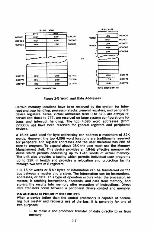
Figure 2·5 Word and Byte Addresses
Certain memory locations have been reserved by the system for inter· rupt and trap handling, processor stacks, general registers, and peripheral device registers. K.ernel virtual addresses from 0 to 370, are always reserved and those to 777, are reserved on large system configurations for traps and interrupt handling. The top 4,096 word addresses (from 770000, up) have been reserved for general registers and peripheral devices.
A 16-bit word used for byte addressing can address a maximum of 32K words. However, the top 4,096 word locations are traditionally reserved for peripheral and register addresses and the user therefore has 28K of core to program. To expand above 28K the user must use the Memory Management Unit. This device provides an 18-bit effective memory ad· dress which permits addressing up to 124K words of actual memory. The unit also provides a facility which permits individual user programs up to 32K in length and provides a relocation and protection facility through two sets of 8 registers.
Full 16-bit words or 8-bit bytes of information can be transferred on the bus between a master and a slave. The information can be instructions, addresses, or data. This type of operation occurs when the processor, as master, is fetching instructions, operands, and data from memory, and storing the results into memory after execution of instructions. Direct data transfers occur between a peripheral device control and memory.
2.6 AUTOMATIC PRIORITY INTERRUPTS When a device (other than the central processor) is capable of becom· ing bus master and requests use of the bus, it is generally for one of two purposes:
1. to make a non-processor transfer of data directly to or from memory
2·7

2. to interrupt a program execution and force the processor to go to a specific address where an interrupt service routine is located.
Direct memory or direct data transfers can be accomplished between any two peripherals without processor supervision. These non-processor request transfers, called NPR level data transfers, are usually made for Direct Memory Access (memory to/from mass storage) or direct device transfers (disk refreshing a CRT display).
The PDP·ll has a multi-line, multi-level priority interrupt structure.
DEVICE CP REQUEST
PRIORITY LINE
4--NPR-------,--------,---------,------------
B~GkJ - BR7 -------,-----------,---------------------- - - -- -
cbcb t::
4--BR6 ------=--,--------=-.r-------------------------~
~ ~ : ~ -•••--[f].,--,. --[f]-r-o
2 --[f]-r-o, --- --- -~
-BR4 -----,-[£]-[£]--,---HSP -,dJ-[f],----TP -----
INCREASING PRIORITY
Figure 2-6 UNIBUS Priority
Bus requests from external devices can be made on one of five request lines. Highest priority is assigned to non-processor request (NPR). These are direct memory access type transfers, and are honored by the processor between bus cycles of an instruction execution.
Bus request 7 (BR7) is the next highest priority, and BR4 is the lowest. Levels below BR4 are not implemented in the PDP·ll/40. They are used in larger machines (PDP·ll/45). Thus, a processor priority of 3, 2, 1, or 0 will have the same effect, i.e. all interrupt requests will be granted.
BR7 through BR4 priority requests are honored by the processor between instructions. The priority is hardwired into each device except for the processor, which is programmable. For example, Teletypes are normally assigned to Bus Request line 4.
The processor's priority can be set under program control to one of eight levels using bits 7, 6, and 5 in the processor status register. These bits set a priority level that inhibits granting of bus requests on lower levels
2-8
or on the same level. When the processor's priority is set to a level, for example PS6, all bus requests on BR6 and below are ignored.
When more than one device is connected to the same bus request (BR) line, a device nearer the central processor has a higher priority than a device farther away. Any number of devices can be connected to a given BR or NPR line.
Thus the priority system is two-dimensional and provides each device with a unique priority. Although its priority level is fixed, its actual priority changes as the processor priority varies. Also, each device may be dynamically, selectively enabled or disabled under program control.
Once a device other than the processor has control of the bus, it may do one of two types of operations: data transfers or interrupt operations.
NPR Data Transfers · NPR data transfers can be made between any two peripheral devices without the supervision of the processor. Normally, NPR transfers are between a mass storage device, such as a disk, and core memory. The structure of the bus also permits device-to-device transfers, allowing customer-designed peripheral controllers to access other devices, such as disks, directly.
An NPR device has very fast access to the bus and can transfer at high data rates once it has control. The processor state is not affected by the transfer; therefore the processor can relinquish control while an in· struction is in progress. This can occur at the end of any bus cycles except in between a read·modify-write sequence. An NPR device can gain control of the bus in 2.6 microseconds or less. An NPR device in control of the bus may transfer 16-bit words from memory at memory speed.
2.6.1 Using the Interrupts Devices that gain bus control with one of the Bus Request lines (BR 7 · BR 4), can take full advantage of the Central Processor by requesting an interrupt. In this way, the entire instruction set is available for manipulating data and status registers.
When a service routine is to be run, the current task being performed by the central processor is interrupted, and the device service routine is initiated. Once the request has been satisfied, the Processor returns to its former task.
2.6.2 Interrupt Procedure Interrupt handling is automatic in the PDP-11/40. No device polling is required to determine which service routine to execute. The operations required to service an interrupt are as follows:
1. Processor relinquishes control of the bus, priorities permitting.
2. When a master gains control, it sends the processor an interrupt command and an unique memory address which contains the address of the device's service routine in Kernel virtual address space, called the interrupt vector address. Immediately following this pointer address is a word (located at vector address +2) which is to be used as a new Processor Status Word.
3. The processor stores the current Processor Status Word (PS) and the current Program Counter (PC) into CPU temporary registers.
2-9
4. The new PC and PS (the interrupt vector) are taken from the specified address. The old PS and PC are then pushed onto the current stack as indicated by bits 15,14 of the new PS and the previous mode in effect is stored in bits 13,12 of the new PS. The service routine is th€n initiated.
5. The device service routine can cause the processor to resume the interrupted process by executing the Return from Interrupt (RTI or RTT) instruction, described in Chapter 4, which pops the two top words from the current processor stack and uses them to load the PC and PS registers.
This instruction requires 2.9 ~tsec providing there is no NPR request.
A device routine can be interrupted by a higher priority bus request any time after the new PC and PS have been loaded. If such an interrupt occurs, the PC and the PS of the service routine are automatically stored in the temporary registers and then pushed onto the new current stack, and the new device routine is initiated.
2.6.3 Interrupt Servicing Every hardware device capable of interrupting the processor has a unique set of locations (2 words) reserved for its interrupt vector. The first word contains the location of the device's service routine, and the second, the Processor Status Word that is to be used by the service routine. Through proper use of the PS, the programmer can switch the operational mode of the processor, and modify the Processor's Priority level to mask out lower level interrupts.
2.7 PROCESSOR TRAPS There are a series of errors and programming conditions which will cause the Central Processor to trap to a set of fixed locations. These include Power Failure, Odd Addressing Errors, Stack Errors, Timeout Errors, Memory Parity Errors, Memory Management Violations, Floating Point Processor Exception Traps, Use of Reserved Instructions, Use of the T bit in the Processor Status Word, and use of the lOT, EMT, and TRAP instructions.
2.7.1 Power Failure Whenever AC power drops below 95 volts for 115v power (190 volts for 230v) or outside a limit of 47 to 63 Hz, cts measured by DC power, the power fail sequence is initiated. The Central Processor automatically traps to location 24 and the power fail program has 2 msec. to save all volatile information (data in registers), and condition peripherals for power fail.
When power is restored the processor traps to location 24 and executes the power up routine to restore the machine to its state prior to power failure.
2.7.2 Odd Addressing Errors This error occurs whenever a program attempts to execute a word instruc·
2·10

tion on an odd address (in the middle of a word boundary). The instruction is aborted and the CPU traps through location 4.
2.7.3 Time-out Errors These errors occur when a Master Synchronization pulse is placed on the UNIBUS and there is no slave pulse within 15~sec. This error usually occurs in attempts to address non-existent memory or peripherals.
The offending instruction is aborted and the processor traps through location 4.
2.7.4 Reserved Instructions There is a set of illegal and reserved instructions which cause the processor to trap through location 10.
2.7.5 Trap Handling Appendix B includes a list of the reserved Trap Vector locations, and System Error Definitions which cause processor traps. When a trap occurs, the processor follows the same procedure for traps as it does for interrupts (saving the PC and PS on the new Processor Stack etc. . . .)
In cases where traps and interrupts occur concurrently, the processor will service the conditions according to the following priority sequence.
Odd Addressing Error
Fatal Stack Violations (Red)
Memory Management Violations
Timeout Errors
Trap Instructions
Trace Trap
Warning Stack Violation (Yellow)
Power Failure
Processor Priority level 7
Floating Point Exception Trap
BR 7
• • • • • • • • • •
Processor 0
2-11


CHAPTER 3
ADDRESSING MODES
Data stored in memory must be accessed, and manipulated. Data handling is specified by a PDP·ll instruction (MOV, ADD etc.) which usually indicates:
the function (operation code)
a general purpose register to be used when locating the source operand and/or a general purpose register to be used when locating the destination operand.
an addressing mode (to specify how the selected register(s) is/are to be used)
Since a large portion of the data handled by a computer is usually structured (in character strings, in arrays, in lists etc.), the PDP·ll has been designed to handle structured data efficiently and flexibly. The general registers may be used with an instruction in any of the following ways:
as accumulators. The data to be manipulated resides within the register.
as pointers. The contents of the register are the address of the operand, rather than the operand itself.
as pointers which automatically step through core locations. Automatically stepping forward through consecutive core locations is known as au· toincrement addressing; automatically stepping backwards is known as autodecrement addressing. These modes are particularly useful for pro· cessing tabular data.
as index registers. In this instance the contents of the register, and the word following the instruction are summed to produce the address of the operand. This allows easy access to variable entries in a list.
PDP·ll's also have instruction addressing mode combinations which facilitate temporary data storage structures for convenient handling of data which must be frequently accessed. This is known as the " stack."
In the PDP·ll any register can be used as a "stack pointer"under program con· trol, however, certain instructions associated with subroutine linkage and inter· rupt service automatically use Register 6 as a "hardware stack pointer". For this reason R6 is frequently referred to as the "SP"
R7 is used by the processor as its program counter (PC). It is recommended that R7 not be used as a stack pointer.
An important PDP·ll /40 feature, which must be considered in conjunction with the addressing modes, is the register arrangement;
3·1

Six general purpose registers (RO-R5)
A hardware stack pointer (R6), (2 with Memory Management)
A Program Counter (PC) register (R7).
Instruction mnemonics and address mode symbols are sufficient for writing machine language programs. The programmer need not be concerned about conversion to binary digits; this is accomplished automatically by the PDP-11 MACRO Assembler.
3.1 SINGLE OPERAND ADDRESSING The instruction format for all single operand instructions (such as clear, increment, test) is:
MODE Rn
~1~5 __________ ~----------~6 5 4 3 2 0
OP CODE ____ ___,
DESTINATION ADDRESS------------------------'
Bits 15 through 6 specify the operation code that defines the type of instruction to be executed.
Bits. 5 through 0 form a six-bit field called the destination address field. This consists of two subfields:
a) Bits 0 through 2 specify which of the eight general purpose registers is to be referenced by this instruction word.
b) Bits 3 through 5 specify how the selected register will be used (address mode). Bit 3 indicates direct or deferred (indirect) addressing.
3.2 DOUBLE OPERAND ADDRESSING Operations which imply two operands (such as add, subtract, move and compare) are handled by instructions that specify two addresses. The first operand is called the source operand, the second the destination operand. Bit assignments in the source and destination address fields may specify different modes and different registers. The Instruction format for the double operand instruction is:
3-2

OP CODE MODE An MODE Rn
15 12 11 10 9 8 6 5 4 0
SOURCE ADDRESS------I OE"STINATION ADORESS----------__J
The source address field is used to select the source operand, the first operand. The destination is used similarly, and locates the second op· erand and the result. For example, the instruction ADD A, B adds the contents (source operand) of location A to the contents (destination operand) of location B. After execution B will contain the result of the addition and the contents of A will be unchanged.
Examples in this section and further in this chapter use the following sample PDP·ll instructions:
Mnemonic Description Octal Code
CLR clear (zero the specified destination) 0050DD
CLRB clear byte (zero the byte in the specified 1050DD destination)
INC increment (add 1 to contents of destination) 0052DD
I NCB increment byte (add 1 to the contents of 1052DD destination byte)
COM complement (replace the contents of the 0051DD destination by their logical complement; each 0 bit is set and each 1 bit is cleared)
COMB complement byte (replace the contents of the 1051DD destination byte by their logical complement; each 0 bit is set and each 1 bit is cleared).
ADD add (add source operand to destination 06SSDD operand and store the result at destination address)
DD = destination field (6 bits)
SS =source field (6 bits)
) = contents of
3·3

3.3 DIRECT ADDRESSING The following table summarizes the four basic modes used with direct addressing.
DIRECT MODES
Mode Name Assembler Function Syntax
0 Register Rn Register contains operand
2 Autoincrement (Rn)+ Register is used as a pointer to sequential data then in· crernented
4 Autodecrement -(Rn) Register is decremented and then used as a pointer.
6 Index X(Rn) Value X is added to (Rn) to pro· duce address of operand. Nei· ther X nor (Rn) are modified.
3.3.1 Register Mode OPR Rn
With register mode any of the general registers may be used as simple accumula· tors and the operand is contained in the selected register. Since they are hard· ware registers, within the processor, the general registers operate at high speeds and provide speed advantages when used for operating on frequently·accessed variables. The PDP·ll assembler interprets and assembles instructions of the form OPR Rn as register mode operations. Rn represents a general register name or number and OPR is used to represent a general instruction mnemonic. As· sembler syntax requires that a general register be defined as follows:
(% sign indicates register definition) R0=%0
Rl-%1
R2-%2, etc.
Registers are typically referred to by name as RO, Rl, R2, R3, R4, R5, R6 and R7. However R6 and R7 are also referred to as SP and PC, respectively.
Registw Mode Examples (all numbers in octal)
Symbolic
1. INCR3
Oper•tion:
Octal Code Instruction Name
005203 Increment
Add one to the contents of general register 3
3·4

R0
Rl
loooo1o1o o!oojo!o ~~~ ~~~5~==~=~====~====:====:~6~5.-.4-,3~~--~0
R2
,. R3
R4
OP CODE (1NC(0052))_j R5
DESTINATION FIELD--------------------' R6(SP)
2. ADDR2,R4
Operation:
3. COMBR4
Operation:
R7 (PC)
060204 Add
Add the contents of R2 to the contents of R4.
BEFORE AFTER
R21 000002 R21 000002
R41 000004 R41 000006
BEFORE
105104 Complement Byte
One's complement bits 0.7 (byte) in R4. (When general registers are used, byte instructionS' only operate on bits 0-7; i.e. byte 0 of the register)
AFTER
1141 022222 R41 022155
3.3.2 Autoincrwnent Mode OPR (Rn)+
This mode provides for automatic stepping of a pointer through sequential elements of a table of operands. It assumes the contents of the selected general reg· ister to be the address of the operand. Contents of registers are stepped (by one for bytes, by two for words, always by two for R6 and R7) to address the next se· quentiallocation. The autoincrement mode is especially useful for array process· ing and stacks. It will access an element of a table and then step the pointer to address the next operand in the table. Although most useful for table handling, this mode is completely general and may be used for a variety of purposes.
3·5
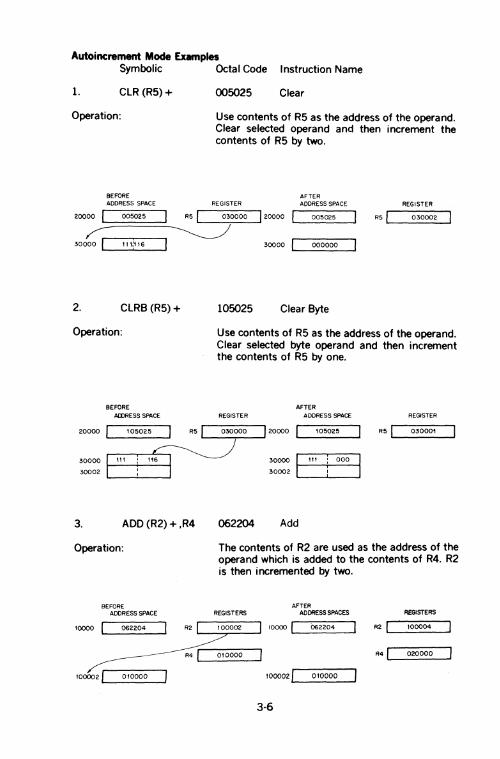
Autoincrement Mode Examples Symbolic Octal Code Instruction Name
1. CLR (R5)+
Operation:
BEFORE ADDRESS SPACE
20000 I 005025 I R5 I
005025 Clear
Use contents of R5 as the address of the operand. Clear selected operand and then increment the contents of R5 by two.
AFTER REGISTER ADDRESS SPACE REGISTER
030000 120000 005025 Rsj 030002
~ 1 111!116 1 30000
2. CLRB(R5)+
Operation:
BEFORE AOORESS SPACE
20000 I 105025 I R5 I
30000 000000
105025 Clear Byte
Use contents of R5 as the address of the operand. Clear selected byte operand and then increment the contents of R5 by one.
AFTER
REGISTER ADDRESS SPACE REGISTER
030000 120000 105025 R51 030001
~ 30000 30000 111 000
30002 30002
3. ADD (R2) + ,R4
Operation:
BEFORE ADDRESS SPACE
062204 Add
The contents of R2 are used as the address of the operand which is added to the contents of R4. R2 is then incremented by two.
AFTER REGISTERS ADDRESS SPACES REGISTERS
10000 062204 ~ 10000 1 062204 R2 [ 100004
R41 020000 -- R4 I 010000 I ,---;:_
1000021 010000 100002/ 010000
3-6

3.3.3 Autodecrement Mode OPR-(Rn)
This mode is useful for processing data in a list in reverse direction. The contents of the selected general register are decremented (by two for word instructions, by one for byte instructions) and then used as the address of the operand. The choice of postincrement, predecrement features for the PDP·ll were not arbitrary decisions, but were intended to facilitate hardware/software stack operations.
Autodecrement Mode Examples Symbolic Octal Code Instruction Name
1. INC-(RO)
Operation:
BEFORE ADDRESS SPACE
10001 005240 R0.,
17774 1 000000
2. INCB-(RO)
Operation:
BEFORE
005240 Increment
The contents of RO are decremented by two and used as the address of the operand. The operand is increased by one.
AFTER REGISTERS ADDRESS SPACE REGISTER
017776 10001 005240 R01 017774
17774 1 000001
105240 Increment Byte
The contents of RO are decremented by one then used as the address of the operand. The operand byte is increased by one.
AFTER
REGISTER ADDRESS SPACE ADDRESS SPACE
1000 LI_.:..:10:..:5::..2•:..:o_...J R01 L _..:.0...:.17_77...:.6-....1
17774 I 000
17776 L. --'---....1
000
3. ADD-(R3).RO
Operation:
064300
17774 ,_.._::::.:..__;_.:..:..:~ 17776 L_ _ __;_ _ _.J
Add
The contents of R3 are decremented by 2 then used as a pointer to an operand (source) which is added to the contents of RO (destination operand).
3-7

BEFORE AFTER ADDRESS SPACE REGISTER ADDRESS SPACE REGISTER
10020 1 064300 R01 000020 10020 1 064300 R01 0000070
R31 077776
777741 000050 000050
77776
3.3.4 Index Mode OPR X(Rn)
The contents of the selected general register, and an index word following the instruction word, are summed to form the address of the operand. The contents of the selected register may be used as a base for calculating a series of addresses, thus allowing random access to elements of data structures. The selected register can then be modified by program to access data in the table. Index addressing instructions are of the form OPR X(Rn) where X is the indexed word and is located in the memory location following the instruction word and Rn is the selected general register.
Index Mode Examples Symbolic
1. CLR 200(R4)
Operation:
BEFORE
AOORESS SPACE
Octal Code Instruction Name
005064 000200
Clear
The address of the operand is determined by ad· ding 200 to the contents of R4. The location is then cleared.
AFTER
REGISTER ADDRESS SPACE REGISTER
1020 §§05064 R4 I 001000
1022 000200
1024 1000 11:::: 1200 177777
1202
2. COMB 200(R1)
Operation:
105161 000200
1200E3
Complement Byte
The contents of a location which is determined by adding 200 to the contents of Rl are one's com· plernented. (i.e. logically complemented)
3·8

3.
1020 1---~:..::....--l 1022 1----'==--1
REGISTER
R1 ._l __ D_17_7_7_,_~
ADD 30(R2),20(R5) 066265 000030 000020
AFTER
ADDRESS SPACE
10201----:-~.:.,..,.--l 1022 f-_.:;.:..:;::.;:_;__-l
20176 ~--''6"'6"':oc.:o.,;.o_-l 20200 L-. __ ..__ _ __J
Add
REGISTER
R 1 L.l _ _:o:..:.•...:n..;.'...:'_..J
Operation: The contents of a location which is determined by adding 30 to the contents of R2 are added to the contents of a location which is determined by ad· ding 20 to the contents of RS. The result is stored at the destination address, i.e. 20(R~)
BEFORE AFTER
AOORESS SPACE REGISTER ADDRESS SPACE REGISTER
1020 I 066265 R2 I 001100 10201 066265 R2J 001100
1022 I 000030 1022 1 000030
1o24 1 000020 R5 I 002000 1o24 1 000020 R51 002000
1130 1 o00001 1130 1 000001
2020 1 000001 2020 1 000002
t100 2000 +30 +20
""i"i3ci"" 2ii2o
3-9

3.4 DEFERRED (INDIRECT) ADDRESSING The four basic modes may also be used with deferred addressing. Whereas in the register mode the operand is the contents of the selected register, in the register deferred mode the contents of the selected register is the address of the operand.
In the three other deferred modes, the contents of the register selects the address of the operand rather than the operand itself. These modes are therefore used when a table consists of addresses rather than operands. Assembler syntax for indicating deferred addressing is "@" (or "( )" when this not ambiguous). The following table summarizes the deferred versions of the basic modes:
Mode Name Assembler Syntax
Function
1 Register Deferred @Rn or (Rn) Register contains the address of the operand
3 Autoincrement Deferred @(Rn) + Register is first used as a pointer to a word containing the address of the operand, then in· cremented (always by 2; even for byte instructions).
5 Autodecrement Deferred @-(Rn) Register is decremented (alw_!!ys by two; even for byte instruc· tions) and then used as a pointer to a word containing the address of the operand
7 Index Deferred @X(Rn) Value X (stored in a word follow· ing the instruction) and (Rn) are added and the sum is used as a pointer to a word containing the address of the operand. Neither X nor (Rn) are modified.
Since each deferred mode is similar to its basic mode counterpart, separate de· scriptions of each deferred mode are not necessary. However, the following exam· pies illustrate the deferred modes.
Register Deferred Mode Example Symbolic Octal Code Instruction Name
CLR @R5
Operation:
BEFORE ADDRESS SPACE
11100677/r---------i 0 000100
005015 Clear
The contents of location specified in R5 are cleared.
AFTER
REGISTER ADDRESS SPACE REGISTER
Rs ,_I _oo_1r_oo _ _, t6771 1700 1-_ -0-:-::0000-:-:-::-0--;
R5 L-1 _oo_1r_oo _ _,
3-10

Autoincrement Deferred Mode Example Symbolic Octal Code Instruction Name
INC@(R2)+
Operation:
BEFOOE
ADDRESS SPACE
005232 Increment
The contents of R2 are used as the address of the address of the operand. Operand is increased by one. Contents of R2 is incremented by 2.
AFTER
REGISTER ADDRESS SPACE REGISTER
~ R21 010300
~/// 1010~ 1012~
R2 Ll __ o1_o_,o_2_..J
10300 I 001010 10300 ~--1--'-00.:_1_0_10 _ _,
Autodecrement Deferred Mode Example
Symbolic
COM @-(RO)
Operation:
BEFORE ADDRESS SPACE
10100 1----.:.01_:23:._4.:._5 --1
10102 1-------1
10774 ~--'-0-'-1 0.:_1 0:..:0--.:.-1
10776 L. ____ ....J
Octal Code Complement
005150
The contents of RO are decremented by two and then used as the address of the address of the operand. Operand is one's complemented. (i.e. logically complemented)
AFTER
REGISTER ADDRESS SPACE REGISTER
R0 Ll __ o_1 o_7_7s_..J 10100 I 165432 I R01 010774
101~---
:~;:1 010100 I
Index Deferred Mode Example Symbolic Octal Code Instruction Name
ADD @ 1000(R2),R1 067201 Add 001000
Operation: 1000 and contents of R2 are summed to produce the address of the address of the source operand the contents of which are added to contents of Rl; the result is stored in Rl.
3-11

BEFORE AFTER ADDRESS SPACE 1-fi:.GISTER ADORES S SPACE REGISTER
1020 067201 I R1 I 001234 1020 1 067201 R1 I 001236
1022 001000 I R2 I 000100 1022 1 001000
R2 I 000100 1024 I 10241
1050 I 000002 1050 I 000002
\J:~ 11~~?gg 1100 I 001050
1100
3.5 USE OF THE PC AS A GENERAL REGISTER Although Register 7 is a general purpose register, it doubles in function as the Program Counter for the PDP-11. Whenever the processor uses the program counter to acquire a word from memory, the program counter is automatically incremented by two to contain the address of the next word of the instruction being executed or the address of the next instruction to be executed. (When the program uses the PC to locate byte data, the PC is still incremented by two.)
The PC responds to all the standard PDP-11 addressing -modes. However, there are four of these modes with which the PC can provide advantages for handling position independent code (PIC- seeChapter 5) and unstructured data. When regarding the PC these modes are termed immediate, absolute (or immediate deferred), relative and relative deferred, and are summarized below:
Mode Name
2 Immediate
3 Absolute
6 Relative
7 Relative Deferred
Assembler Function Syntax
# n Operand follows instruction
@#A Absolute Address follows instruction
A Relative Address (index value) follows the instruction.
@A Index value (stored in the word following the instruction) is the relative address for the address of the operand.
The reader should remember that the special effect modes are the same as modes described in 3.3 and 3.4, but the general register selected is R7, the program counter.
When a standard program is available for different users, it often is helpful to be able to load it into different areas of core and run it there. PDP-11 'scan accomplish the relocation of a program very efficiently through the use of position inde-
3-12

pendent code (PIC) which is written by using the PC addressing modes. If an in· struction and its objects are moved in such a way that the relative distance between them is not altered. the same offset relative to the PC can be used in all positions in memory. Thus, PIC usually references locations relative to the current location. PIC is discussed in more detail in Chapter 5.
The PC also greatly facilitates the handling of unstructured data. This is partie· ularly true of the immediate and relative modes.
3.5.1 Immediate Mode OPR #n,DD
Immediate mode is equivalent to using the autoincrement mode with the PC. It provides time improvements for accessing constant operands by including the constant in the memory location immediately following the instruction word.
Immediate Mode Example Symbolic
ADD #lO,RO
Operation:
BEFORE ADDRESS SPACE
t020 062700 ""R01 1022 000010 PC 1024
3.5.2 Absolute Addressing
Octal Code Instruction Name
062700 Add 000010
The value 10 is located in the second word of the instruction and is added to the contents of RO. Just before this instruction is fetched and exe· cuted, the PC points to the first word of the in· struction. The processor fetches the first word and increments the PC by two. The source operand mode is 27 (autoincrement the PC). Thus, the PC is used as a pointer to fetch the operand (the sec· ond word of the instruction) before being in· cremented by two to point to the next instruction.
AFTER
REGISTER ADDRESS SPACE REGISTER
000020 1020 062700 I R01 000030
1022 000010 1_.---Pc t024 I
OPR @#A
This mode is the equivalent of immediate deferred or auto increment deferred us· ing the PC. The contents of the location following the instruction are taken as the address of the operand. Immediate data is interpreted as an absolute address (i.e., an address that remains constant no matter where in memory the as· sembled instruction is executed).
3·13

Absolute Mode Examples Symbolic
1. CLR @#1100
Operation:
BEFORE
ADDRESS SPACE
20
22
1100 I 177777
1102
Octal Code Instruction Name
005037 001100
Clear
Clear the contents of location 1100.
AFTER
ADDRESS SPACE
20
PC 22
24
1100 E 000000
1102
/PC
2. ADD@# 2000,R3 063703 002000
Operation: Add contents of location 2000 to R3.
BEFORE AFTER
ADDRESS SPACE REGISTER ADDRESS SPACE REGISTER
20 1-_.:..:.;:..c:..:...._---1 000500 20 R31 001000
22 1-_.:.=:..:..._---1 22
24
2000 I 000300
24 ~-=------1 /;.-------
2000 I 000300
3.5.3 Relative Addressing OPR A or
OPR X(PC) , where X is the location of A relative to the instruction.
This mode is assembled as index mode using R7. The base of the address calcu· lation, which is stored in the second or third word of the instruction, is not the ad· dress of the operand, but the number which, when added to the (PC), becomes the address of the operand. This mode is useful for writing position independent code (see Chapter 5) since the lo~ation referenced is always fixed relative to the PC. When instructions are to be relocated, the operand is moved by the same amount.
3·14

Relative Addressing Example Symbolic Octal Code Instruction Name
INC A 005267 Increment 000054
Operation: To increment location A, contents of memory location immediately following instruction word are added to (PC) to produce address A. Contents of A are increased by one.
BEFORE AFTER
ADDRESS SPACE ADDRESS SPACE
1020 0005267
1022 000054
1024 -ec
1020 1-__::00;:.:5::.26::.:7_-1
1022 000054 ~PC 1024 1-------l
1026 ~-----l 1026
,,00 1 000001
1024
101~1~';,~
3.5.4 Relative Deferred Addressing OPR@A or
OPR@X(PC), where x is location containing address of A, relative to the in-struction.
This mode is similar to the relative mode, except that the second word of the instruction, when added to the PC, contains the address of the address of the oper· and, rather than the address of the operand.
Relative Deferred Mode Example Symbolic Octal Code Instruction Name
CLR@A
Operation:
BEFORE
ADDRESS SPACE
1020 1-__:..::..:..:....:._--l' 1022 ~PC
1024 1-------1
10~ )0~6 ~ ~1044 10100 I 100001 I
005077 000020
Clear
Add second word of instruction to PC to produce address of address. of operand. Clear operand.
AFTER
ADDRESS SPACE
1022 '---ec 1024
10441 .010100
101001 000000
3·15

3.6 USE OF STACK POINTER AS GENERAL RE:GISTER The processor stack pointer (SP, Register 6) is in most cases the general register used for the stack operations related to program nesting. Autodecrement with Register 6 "pushes" data on to the stack and autoincrement with Register 6 "pops" data off the stack. Index mode with SP permits random access of items on the stack. Since the SP is used by the processor for interrupt handling, it has a special attribute: autoincrements and autodecrements are always done in steps of two. Byte operations using the SP in this way leave odd addresses unmodified.
With the Memory Management option there are two R6 registers selected by the PS; but at any given time there is only one in operation.
3.7 SUMMARY OF ADDRESSING MODES
3.7.1 General Register Addressing
R is a general register, 0 to 7 (R) is the contents of that register
ModeO Register OPR R R contains operand
R
I INSTRUCTION ~ OPERAND
Mode 1 Register deferred OPR (R) R contains address
Mode 2 Auto-increment OPR (R)+
R contains address, then increment (R)
3-16

Mode 3 Auto-increment OPR @(R)+ deferred
Mode4 Auto-decrement
Decrement (R), then R contains address
R contains address of address, then increment (R) by 2
OPR -(R)
Mode 5 Auto-decrement deferred
OPR @-(R) Decrement (R) by 2, then R contains address of address
R
I INSTRUCTION ~ ADDRESS f----l....__-_2 --~T ADDRESS ~ OPERAND
Mode6 Index OPR X(R) (R) + X is address
ADDRESS ~r--0-f'E-R-AN-D-,
Mode 7 Index deferred OPR @X(R) (R) + X is address of address
3-17

3.7.2 Program Counter Addressing
Register= 7
Mode2 Immediate OPR #n
PC 'INSTRUCTION I PC+2 ... I ___ _,
Model Absolute OPR @#A
PC 'INSTRUCTION I PC+2 ._1 __ A _ __,f-------1 OPERAND
Mode6 Relative OPR A
PC 'INSTRUCTION I
.... : . ~ PCt4 i NEXT INSTR I + A
OPERAND
Mode 7 Relative deferred OPR @A
Operand n follows instruction
Address A follows instruction
PC+ 4 +X is address '-v-'
updated PC
PC+ 4 +X is address of address '-v-'
updated PC
3·18

CHAPTER 4
INSTRUCTION SET
4.1 INTRODUCTION
The specification for each instruction includes the mnemonic, octal code, binary code, a diagram showing the format of the instruction, a symbolic notation describing its execution and the effect on the condition codes, a description, special comments, and examples.
MNEMONIC: This is indicated at the top corner of each page. When the word instruction has a byte equivalent, the byte mnemonic is also shown.
INSTRUCTION FORMAT: A diagram accompanying each instruction shows the octal op code, the binary op code, and bit assignments. (Note that in byte instructions the most significant bit (bit 15) is always a 1.)
SYMBOLS:
( ) = contents of
SS or src = source address
DD or dst = destination address
loc = location
+-=becomes
t = "is popped from stack"
J, ="is pushed onto stack"
A = boolean AND
v = boolean OR
..Y..= exclusive OR
- = boolean not
Reg or R = register
B =Byte
• = {0 for word
1 for byte
4·1

4.2 INSTRUCTION FORMATS The major instruction formats are:
15
15
15
15
Single Operand Group
OP Code I
Double Operand Group
OP Code I
12 11
Src I
Register-Source or Destination
OPCode I :reg '
9 8
Branch
1ease ~ode I
8 7
4·2
dst
6 5
6 5
6 5
dst I
Src/dst I
offset I
0
0
0
0

Byte Instructions The POP-11 processor includes a full complement of instructions that manipulate byte operands. Since all POP-11 addressing is byte-oriented, byte manipulation addressing is straightforward. Byte instructions with autoincrement or autodecrement direct addressing cause the specified register to be modified by one to point to the next byte of data. Byte operations in register mode access the low-order byte of the specified register. These provisions enable the POP-11 to perform as either a word or byte processor. The numbering scheme for word and byte addresses in core memory is:
HIGH BYTE ADDRESS
002001
002003
BYTE
BYTE
1
3
BYTE 0
BYTE 2
\\ORO OR BYTE ADDRESS
002000
002002
The most significant bit (Bit 15) of the instruction word is set to indicate a byte instruction.
Example:
Symbolic Octal
CLR CLRB
005000 105000
4-3
Clear Word Clear Byte

4.3 LIST OF INSTRUCTIONS The PDP·ll/40 instruction set is shown in the following sequence.
SINGLE OPERAND
Mnemonic
General CLR(B) COM(B) INC( B) DEC( B) NEG(B) TST(B)
Shift & Rotate ASR(B) ASL(B) ROR(B) ROL(B) SWAB
Instruction
clear destination complement dst increment dst decrement dst ........... .. negate dst .... test dst
arithmetic shift right ... . arithmetic shift left .... . rotate right ... . rotate left .. . swap bytes . .. ................................. .
Multiple Precision ADC(B) add carry . . . ................. .. SBC(B) subtract carry .................................... .. SXT sign extend ......................................... .
DOUBLE OPERAND
General MOV(B) CMP(B) ADD SUB
Logical BIT(B) BIC(B) BIS(B)
Register MUL DIV ASH ASHC XOR
move source to destination .............. .. compare src to dst .......................... . add src to dst .................................... . subtract src from dst ......................... ..
bit test ................ . bit clear ........ . bit set .............. ..
multiply ............................................ . divide .............................................. .. shift arithmetically ............................ .. arithmetic shift combined . exclusive OR .................................... .
4·4
OpCode Page
•050DD •051DD •052DD •053DD •054DD •057DD
•0620D •063DD •060DD •061DD 0003DO
•055DD •056DD 0067DD
•1SSDD •2SSDD 06SSDD 16SSDD
•3SSOD •4SSDD •5SSDO
070RSS 071RSS 072RSS 073RSS 074RDD
4·6 4-7 4-8 4·9 4·10 4-11
4-13 4·14 4-15 4·16 4·17
4·19 4·20 4·21
4·23 4·24 4-25 4·26
4·28 4·29 4-30
4·31 4·32 4-33 4-34 4-35

PROGRAM CONTROL
Mnemonic
Branch BR BNE BEQ BPL BMI BVC BVS BCC BCS
Instruction
branch (unconditional) ...................... . branch if not equal (to zero) ... . branch if equal (to zero) .................... . branch if plus ... branch if minus branch if overflow is clear . branch if overflow is set ............ . branch if carry is clear . branch if carry is set ................. .
Signed Conditional Branch BGE branch if greater than or equal
(to zero) ................... . BL T branch if less than (zero) BGT branch if greater than (zero) ... BLE branch if less than or equal (to zero) ....
Unsigned Conditional Branch BHI branch if higher ........................ . BLOS branch if lower or same ................ . BHIS branch if higher or same ............. . BLO branch if lower ......................... .
Jump & Subroutine JMP jump ....................................... . JSR jump to subroutine ............................ . RTS return from subroutine MARK mark .................................................... . SOB subtract one and branch (if :I= 0) ....... .
Trap & Interrupt
OpCode or
Base Code Page
000400 001000 001400 100000 100400 102000 102400 103000 103400
002000 002400 003000 003400
101000 101400 103000 103400
000100 004ROO 00020R 006400 077ROO
4·37 4'38 4·39 4·40 4·41 4·42 4·43 4·44 4-45
4-47 4·48 4·49 4-50
4·52 4-53 4·54 4·55
4·56 4-58 4·60 4-61 4·63
EMT emulator trap .. .... .... .... .. ..... 104000-104377 4·65 TRAP trap . . . . . . . . . . . . . . .. . . .. . . .. . . . . . . . . . . . . . 104400-104777 4·66 BPT breakpoint trap . . . . . . . .. . . .. . .. . . . . . . . . . . . . . . .. . . . 000003 4-67 lOT input/ output trap . . . . . . . . . . . . . . 000004 4·68 RTI return from interrupt ............................ 000002 4·69 RTI return from interrupt ......... .................. 000006 4-70
MISCELLANEOUS HALT halt.......................... ... . . ........... . 000000 4·74 WAIT wait for interrupt . . . . . . . . . . ............. . 000001 4·75 RESET reset external bus .................... . 000005 4·76 MFPI move from previous instruction space .. 0065SS 4·77 MTPI move to previous instruction space ..... . 006600 4·78
Condition Code Operation CLC, CLV, CLZ, CLN, CCC clear ...................... . 000240 4·79 SEC, SEV, SEZ, SEN, SCC set ......................... . 000260 4-79
4·5

4.4 SINGLE OPERAND INSTRUCTIONS
CLR CLRB
clear destination
0 0 0
15
Operation: (dst).O
Condition Codes: N: cleared Z: set V: cleared C: cleared
0 : 0
•050DD
d d d
6 5 0
Description: Word: Contents of specified destination are replaced with zeroes.
Example:
Byte: Same
Before (R1) = 177777
NZVC 1 1 1 1
4·6
CLR Rl
After (R1) = 000000
NZVC 0100

COM COMB
complement dst •05100
0 0 0 : 0 1 I d d d d d I d I I
0
15 6 5 0
Op_..tion: (dst).-(dst)
Condition Codes: N: set if most significant bit of result is set; cleared otherwise Z: set if result is 0; cleared otherwise V: cleared C: set
Description: Replaces the contents of the destination address by their logical complement (each bit equal to 0 is set and each bit equal to 1 is cleared) Byte: Same
Example: COM RO
Before (RO) = 013333
NZVC 0110
4-7
After (RO) = 164444
NZVC 1001

INC I NCB
increment dst •05200
0 0 0 d d
15 6 5
Operation: (dst).(dst) + 1
Condition Codes: N: set if result is <0; cleared otherwise Z: set if result is 0; cleared otherwise
d
V: set if (dst) held 077777; cleared otherwise C: not affected
Description: Word: Add one to contents of destination Byte: Same
Example: INC R2
d
Before (R2) = 000333
After (R2) = 000334
NZVC 0000
4-8
NZVC 0000
0

DEC DECB
decrement dst •05300
0 0 0 d d
15 6 5
Opwation: (dst)4(dst)-1
Condition Codes: N: set if result is < 0; cleared otherwise Z: set if result is 0; cleared otherwise
d
V: set if (dst) was 100000; cleared otherwise C: not affected
d
0
Description: Word: Subtract 1 from the contents of the destination Byte: Same
Example: DEC R5
Before (R5) = 000001
NZVC 1000
4-9
After (R5) = 000000
NZVC 0100

NEG NEGB
negate dst •05400
jot1 I o 0 0 0 d d d I
15 6 5
Operation: (dst). -(dst)
Condition Codes: N: set if the result is <0; cleared otherwise Z: set if result is 0; cleared otherwise V: set if the result is 100000; cleared otherwise C: cleared if the result is 0; set otherwise
d
0
Description: Word: Replaces the contents of the destination address by its two's complement. Note that 100000 is replaced by itself ·(in two's complement notation the most negative number has no positive counterpart). Byte: Same
Example: NEG RO
Before (RO) = 000010
NZVC 0000
4·10
After (RO) = 177770
NZVC 1001

test dst
,011 I o 0 0 0 1 : 1
15
Operation: (dst)""l(dst)
d
6 5
d d I
TST TSTB
•05700
d
0
Condition Codes: N: set if the result is <0; cleared otherwise Z: set if result is 0; cleared otherwise V: cleared C: cleared
Description: Word: Sets the condition codes N and Z according to the con· tents of the destination address Byte: Same
Example: TST R 1
Before (R1) = 012340
NZVC 0011
4·11
After (R1) = 012340
NZVC 0000

Shifts Scaling data by factors of two is accomplished by the shift instructions:
ASR - Arithmetic shift right
ASL · Arithmetic shift left
The sign bit (bit 15) of the operand is replicated in shifts to the right The low order bit is filled with 0 in shifts to the left Bits shifted out of the C bit, as shown in the following examples, are lost.
Rotates The rotate instructions operate on the destination word and the C bit as though they formed a 17-bit "circular buffer'. These instructions facilitate sequential bit testing and detailed bit manipulation.
4-12

arithmetic shift right
15 6 5
Operation: (dst)<ot(dst) shifted one place to the right
ASR ASRB
0
Condition Cod•: N: set if the high-order bit of the result is set (result < 0); cleared otherwise Z: set if the result ,. 0; cleared otherwise V: loaded from the Exclusive OR of theN-bit and C-bit (as set by the completion of the shift operation) C: loaded from low-order bit of the destination
Description: Word: Shifts all bits of the destination right one place. Bit 15 is replicated. The C-bit is loaded from bit 0 of the destination. ASR performs signed division of the destination by two. Word:
Byte:
4·13

ASL ASLB
arithmetic shift left •06300
10/1 I o o o 0 , 1 d d d d d d 1 15 6 5 0
Operation: (dst)..(dst) shifted one place to the left
Condition Codes: N: set if high-order bit of the result is set (result < 0); cleared otherwise Z: set if the result = 0; cleared otherwise V: loaded with the exclusive OR of the N-bit and C-bit (as set by the completion of the shift operation) C: loaded with the high-order bit of the destination
Description: Word: Shifts all bits of the destination left one place. Bit 0 is loaded with an 0. The C·bit of the status word is loaded from the most significant bit of the destination. ASL performs a signed multiplication of the destination by 2 with overflow in· dication. Word:
Byte:
~-lL-:: ,......._~, =:!::-:.1 ::-!:-' __.__~r-o0-L-::l ,....._.bl ,.,'-,' ='f::=-1---'--~l-o 15 000 ADDRESS 8 7 EVEN AOORESS 0
4·14

,·otate right
I 0 I 0 : 0 I 0 I d d
15 6 5
d I d
ROR RORB
•06000
0
Condition Codes: N: set if the high-order bit of the result is set (result < 0); cleared otherwise Z: set if all bits of result - 0; cleared otherwise V: loaded with the Exclusive OR of the N-bit and C-bit (as set by the completion of the rotate operation) C: loaded with the low-order bit of the destination
Description:· Rotates all bits of the destination right one place. Bit 0 is loaded into the C-bit and the previous contents of the C-bit are loaded into bit 15 of the destination. Byte: Same
Example: Word:
Byte:
4·15

ROL ROLB
rotate left •06100
1011 I o 0 0
15 6 5
d d I
d
Condition Codes: N: set if the high-order bit of the result word is set (result < 0): cleared otherwise Z: set if all bits of the result word = 0; cleared otherwise V: loaded with the Exclusive OR of the N-bit and C-bit (as set by the completion of the rotate operation) C: loaded with the high-order bit of the destination
Description: Word: Rotate all bits of the destination left one place. Bit 15 is loaded into the C·bit of the status word and the previous contents of the C-bit are loaded into Bit 0 of the destination. Byte: Same
Example: Word:
dst
0-~1 ~~~~~: ~~~~~I L-~1~5 __________________________________ -Jo
Bytes:
4·16

SWAB
swap bytes 0003DD
0 o I o 0 1 1 d
15 6 0
Operation: Byte 1 /Byte 0 .Byte 0/Byte 1
Condition Codes: N: set if high-order bit of low-order byte (bit 7) of result is set; cleared otherwise
Z: set if low-order byte of result = 0; cleared otherwise V: cleared C: cleared
Description: Exchanges high-order byte and low-order byte of the destination word (destination must be a word address).
Example: SWAB Rl
Before (Rl) = 077777
NZVC 1 1 1 1
4-17
After (R1) = 177577
NZVC 0000

Multiple Precision It is sometimes necessary to do arithmetic on operands considered as multiple words or bytes. The PDP·ll makes special provision for such operations with the instructions ADC (Add Carry) and SBC (Subtract Carry) and their byte equiva· Ients.
For example two 16-bit words may be combined into a 32·bit double precision word and added or subtracted as shown below:
32 BIT WORD
OPERAND I At A0
31 16 15
OPERAND I 81 80
31 16 15
RESULT
31 16 15
Example:
The addition of -1 and -1 could be performed as follows:
-1 = 37777777777
D
0
0
(R1) = 177777 (R2) = 177777 (R3) = 177777 (R4) = 177777
ADD R1,R2 ADC R3 ADD R4,R3
1. After (R1) and (R2) are added, 1 is loaded into the C bit
2. ADC instruction adds C bit to (R3); (R3) = 0
3. (R3) and (R4) are added
4. Result is 37777777776 or -2
4·18

add carry
10/1, o 0 0 0 1 1 d
15 6 5
d d d
ADC ADCB
•055DD
d
0
Operation: (dst).(dst) +(C)
Condition Codes: N: set if result <0; cleared otherwise Z: set if result = 0; cleared otherwise V: set if (dst) was 077777 and (C) was 1; cleared otherwise C: set if (dst) was 177777 and (C) was 1; cleared otherwise
Description: Adds the contents of the C·bit into the destination. This per· mits the carry from the addition of the low-order words to be carried into the high-order result. Byte: Same
Example: Double precision addition may be done with the following in· struction sequence: ADD AO,BO ; add low-order parts ADC 81 ; add carry into high-order ADD Al,Bl ; add high order parts
4·19

SBC SBCB
subtract carry
10/1 I o 0 0
15
0
Operation: (dst).(dst)-(C)
, : , d
6 5
Condition Codes: N: set if result <0; cleared otherwise Z: set if result 0; cleared otherwise
d d
V: set if (dst)was 100000; cleared otherwise
•05600
d
0
C: cleared if(dst)was 0 and Cwas 1; set otherwise
Description: Word: Subtracts the contents of the C-bit from the destination. This permits the carry from the subtraction of two loworder words to be subtracted from the high order part of the result Byte: Same
Example: Double precision subtraction is done by:
SUB AO,BO SBC B1 SUB A1,B1
4-20

sign extend
10 ,o 0 0 0
15
Operation: (dst). 0 if N bit is clear ( dst). -1 N bit is set
Condition Codes: N: unaffected Z: set if N bit clear V: unaffected C: unaffected
SXT
006700
d d I d d
6 5 0
Description: If the condition code bit N is set then a -1 is placed in the destination operand: if N bit is clear, then a 0 is placed in the destination operand. This instruction is particularly useful in multiple precision arithmetic because it permits the sign to be extended through multiple words.
Example: SXT A
Before (A) =012345
NZVC 1000
4-21
After (A)= 177777
NZVC 1000
4.5 DOUBLE OPERAND INSTRUCTIONS Double operand instructions provide an instruction (and time) saving facility since they eliminate the need for "load"and "save" sequences such as those used in accumulator-oriented machines.
4·22

MOV MOVB
move source to destination •ISSDD
0 d d d d I
15 12 11 6 5 0
Operation: ( dst ).( src)
Condition Codes: N: set if (src) <0; cleared otherwise Z: set if (src) = 0; cleared otherwise V: cleared C: not affected
Description: Word: Moves the source operand to the destination location. The previous contents of the destination are lost. The contents of the source address are not affected. Byte: Same as MOV. The MOVB to a register (unique among byte instructions) extends the most significant bit of the low order byte (sign extension). Otherwise MOVB operates on bytes exactly as MOV operates on words.
Example: MOV XXX.R1 ; loads Register 1 with the contents of memory location; XXX represents a programmer-defined mnemonic used to represent a memory location
MOV # 20,RO ; loads the number 20 into Register 0; "#"indicates that the value 20 is the operand
MOV @#20,-(R6) ; pushes the operand con· tained in location 20 onto the stack
MOV (R6) + ,@ # 177566 ; pops the operand off a stack and moves it into memory location 177566 (terminal print buffer)
MOV Rl.R3 ; performs an inter register transfer
MOVB @ # 177562,@ # 177566 ; moves a character from terminal keyboard buffer to terminal buffer
4-23

CMP CMPB
compare src to dst
10/11 0 d d I d d d
15 12 11 6 5 0
Operation: (src)-(dst) [in detail, (src) + - (dst) + 1]
Condition Codes: N: set if result <0; cleared otherwise Z: set if result = 0; cleared otherwise V: set if there was arithmetic overflow; that is, operands were of opposite signs and the sign of the destination was the same as the sign of the result; cleared otherwise C: cleared if there was a carry from the most significant bit of the result; set otherwise
Description: Compares the source and destination operands and sets the condition codes, which may then be used for arithmetic and logical conditional branches. Both operands are unaffected. The only action is to set the condition codes. The compare is customarily followed by a conditional branch instruction. Note that unlike the subtract instruction the order of oper· ation is (src)-(dst), not (dst)-(src).
4-24

ADD
add src to dst 06SSDD
s
15 12 ,, 6 5
d d d I
d d
0
Operation: (dst).(src) + (dst)
Condition Codes: N: set if result <0; cleared otherwise Z: set if result = 0; cleared otherwise V: set if there was arithmetic overflow as a result of the oper· ation; that is both operands were of the same sign and the result was of the opposite sign; cleared otherwise C: set if thf!re was a carry from the most significant bit of the result; cleared otherwise
Description: Adds the source operand to the destination operand and stores the result at the destination address. The original contents of the destination are lost. The contents of the source are not affected. Two's complement addition is performed.
Examples: Add to register: ADD 20.RO
Add to memory: ADD RI.XXX
Add register to register: ADD Rl.R2
Add memory to memory: ADD@ # 17750,XXX
XXX is a programmer-defined mnemonic for a memory location.
4-25

SUB
subtract src from dst 16SSDD
o 1 , s s s s d d d I d d d
15 12 ,, 6 5 0
Operation: (dst).(dst)-(src) [in detail (dst) .. (dst) + -(src) + 1]
Condition Codes: N: set if result <0: cleared otherwise Z: set if result = 0; cleared otherwise V: set if there was arithmetic overflow as a result of the oper· ation, that is if operands were of opposite signs and the sign of the source was the same as the sign of the result; cleared otherwise C: cleared if there was a carry from the most significant bit of the result: set otherwise
DescritJtion: Subtracts the source operand from the destination operand and leaves the result at the destination address. The orignial contents of the destination are lost. The contents of the source are not affected. In double-precision arithmetic the C· bit, when set. indicates a "borrow".
Example: SUB Rl,R2
Before (R1) =011111 (R2) =012345
NZVC 1 1 1 1
4·26
After (R1)•011111 (R2) = 001234
NZVC 000 0

Logical These instructions have the same format as the double operand arithmetic group. They permit operations on data at the bit level.
4-27
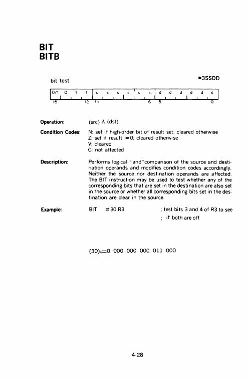
BIT BITB
bit test
15 12 11
Operation: (src) A (dst)
d
6 5
Condition Codes: N: set if high-order bit of result set: cleared otherwise Z: set if result = 0; cleared otherwise V: cleared C: not affected
Description: Performs logical "and"comparison of the source and destination operands and modifies condition codes accordingly. Neither the source nor destination operands are affected. The BIT instruction may be used to test whether any of the corresponding bits that are set in the destination are also set in the source or whether all corresponding bits set in the destination are clear in the source.
Example: BIT #30.R3 : test bits 3 and 4 of R3 to see
: if both are off
(30h=0 000 000 000 011 000
4-28

bit clear
o o 1 • d
15 12 11 6 5
Operation: (dst)•-(src)A(dst)
d d
BIC BICB
•4SSDD
d
0
Condition Codes: N: set if high order bit of result set; cleared otherwise Z: set if result = 0; cleared otherwise V: cleared C: not affected
Description: Clears each bit in the destination that corresponds to a set bit in the source. The original contents of the destination are lost. The contents of the source are unaffected.
Example: BIC R3, R4
Before (R3) =001234
(R4) = 001111
NZVC 1 1 1 1
Before:
After:
After (R3)=001234
(R4) = 000101
NZVC 0001
(R3)=0 000 001 010 011 100 (R4)=0 000 001 001 001 001
(R4)=0 000 000 001 000 001
4-29
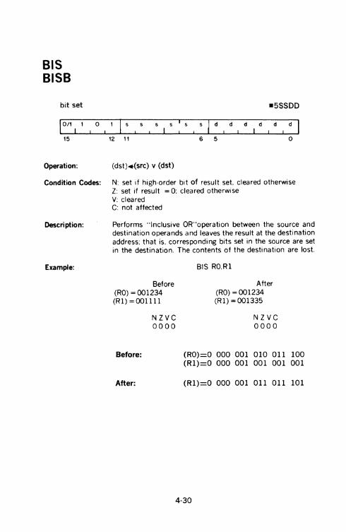
BIS BISB
bit set
15
0
12 11
Operation: (dst)•(src) v (dst)
d d d d
6 5 0
Condition Codes: N: set if high-order bit of result set. cleared otherwise Z: set if result = 0: cleared otherwise V: cleared C: not affected
Description: Performs "Inclusive OR"operation between the source and destination operands and leaves the result at the destination address: that is. corresponding bits set in the source are set in the destination. The contents of the destination are lost
Example: BIS RO,Rl
Before (RO) = 001234 (Rl) =001111
Before:
After:
NZVC 0000
After (RO) = 001234 (R1)=001335
NZVC 0000
(RO)=O 000 001 010 011 100 (R1)=0 000 001 001 001 001
(R1)=0 000 001 011 011 101
4·30

(Ets option>MUL
multiply 070RSS
15 9 8 6 5 0
Operation: R, Rvl• R x(src)
Condition Codes: N: set if product is <0: cleared otherwise Z: set if product is 0; cleared otherwise V: cleared C: set if the result is less than-2•·· or greater than or equal to 2···-1:
Descf'itltion: The contents of the destination register and source taken as two's complement integers are multiplied and stored in the destination register and the succeeding register (if R is even). If R is odd only the low order product is stored. Assembler syntax is : MUL S,R. (Note that the actual destination is R, Rvl which reduces to just R when R is odd.)
Example: 16·bit product (R is odd)
CLC MOV #400,Rl MUL #lO,Rl BCS ERROR
Before
(Rl)=000400
:Clear carry condition code
;Carry will be set if ;product is less than :-2•·· or greater than or equal to 2'' ;no significance lost
After
(R 1) = 004000
4·31

DIV (EIS option)
divide 071RSS
I 0 I , 1 I 0 0 s s s I s 15 9 8 6 5
Operation: R. Rvl• R. Rvl /(src)
Condition Codes: N: set if quotient <0; cleared otherwise Z: set if quotient = 0; cleared otherwise
II s
0
V: set if source = 0 or if the absolute value of the register is larger than the absolute value of the source. (In this case the instruction is aborted because the quotient would exceed 15 bits.) C: set if divide 0 attempted; cleared otherwise
Description: The 32-bit two's complement integer in R andRvl is divided by the source operand. The quotient is left in R; the remainder in Rvl. Division will be performed so that the remainder is of the same sign as the dividend. R must be even.
Example: CLR RO MOV#2000l,Rl DIV#2,RO
Before (RO) = 000000 (R 1),. 020001
After (RO) = 010000 (Rl)"" 000001
4-32
Quotient Remainder

(EIS option) ASH
shift arithmetically 072RSS
I 0 I t t I o s I s t5 9 8 6 5 0
Operation: R• R Shifted arithmetically NN places to right or left Where NN • low order 6 bits of source.
Condition Codes: N: set if result <0; cleared otherwise Z: set if result .. 0; cleared otherwise V: set if sign of register changed during shift; cleared otherwise C: loaded from last bit shifted out of register
Description: The contents of the register are shifted right or left the number of times specified by the shift count. The shift count is taken as the low order 6 bits of the source operand. This number ranges from -32 to + 31. Negative is a a right shift and positive is a left shift.
6 LSB of source 011111 000001 111111 100000
Example:
-I
OR
Action. in general register Shift left 31 places shift left 1 place shift right 1 place shift right 32 places
Before (R3)=001234 (R0)=000003
4-33
ASH RO, R3
1-0 0
1-0 0
After (R3)=012340 (R0)=000003

ASHC (EIS option)
arithmetic shift combined 073RSS
I 0 I t • • 1 I I .
t5 9 8 6 5 0
Operation: R, Rv1.R, Rv1 The double word is shifted NN places to the right or left, where NN =low order six bits or source
Condition Codes: N: set if result <0; cleared otherwise Z: set if result = 0; cleared otherwise V: set if sign bit changes during the shift; cleared otherwise C: loaded with high order bit when left Shift ; loaded with low order bit when right shift (loaded with the last bit shifted out of the 32-bit operand)
Description: The contents of the register and the register ORed with one are treated as one 32 bit word, R + 1 (bits 0-15) and R (bits 16-31) are shifted right or left the number of times specified by the shift count The shift count is taken as the low order 6 bits of the source operand. This number ranges from -32 to + 31. Negative is a right shift and positive is a left shift When the register chosen is an odd number the register and the register OR'ed with one are the same. In this case the right shift becomes a rotate (for up to a shift of 16). The 16 bit word is rotated right the number of bits specified by the shift count
[ I I P'
I I ___j 16
• R+1 I I 1-GJ 15 0
rL~--------~----:===~~--------------~ R+1 I f-o
4-34

XOR
exclusive OR 074RDD
15 9 8 6 5
Operation: (dst).Rv(dst)
Condition Codes: N: set if the result <0: cleared otherwise Z set if result = 0: cleared otherwise V: cleared C: unaffected
d d 1 0
Description: The exclusive OR of the register and destination operand is stored in the destination address. Contents of register are unaffected. Assembler format is: XOR R.D
Example: XOR RO,R2
Before (RO) = 001234 (R2) = 001111
Before:
After:
After (RO) = 001234 (R2) = 000325
(RO)=O 000 001 010 011 100 (R2)=0 000 001 001 001 001
(R2)=0 000 000 011 010 101
4·35
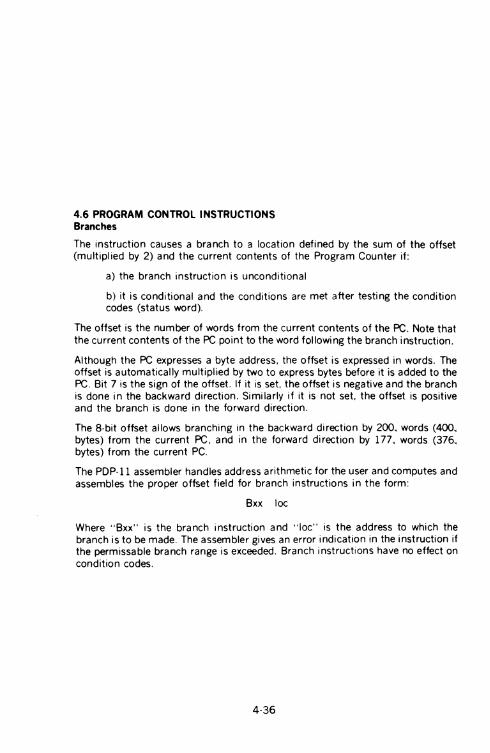
4.6 PROGRAM CONTROL INSTRUCTIONS Branches
The instruction causes a branch to a location defined by the sum of the offset (multiplied by 2) and the current contents of the Program Counter if:
a) the branch instruction is unconditional
b) it is conditional and the conditions are met after testing the condition codes (status word).
The offset is the number of words from the current contents of the PC. Note that the current contents of the PC point to the word following the branch instruction.
Although the PC expresses a byte address, the offset is expressed in words. The offset is automatically multiplied by two to express bytes before it is added to the PC. Bit 7 is the sign of the offset. If it is set, the offset is negative and the branch is done in the backward direction. Similarly if it is not set, the offset is positive and the branch is done in the forward direction.
The 8-bit offset allows branching in the backward direction by 200, words (400, bytes) from the current PC, and in the forward direction by 177, words (376, bytes) from the current PC.
The PDP-11 assembler handles address arithmetic for the user and computes and assembles the proper offset field for branch instructions in the form:
Bxx loc
Where "Bxx" is the branch Instruction and "loc" is the address to which the branch is to be made. The assembler gives an error indication in the instruction if the permissable branch range is exceeded. Branch instruct1ons have no effect on condition codes.
4·36

BR
branch (unconditional) 000400 Plus offset
1000000011 OFFSET
15 8 7 0
Operation: PC • PC + (2 x offset)
Description: Provides a way of transferring program control within a range of -128 to + 127 words with a one word instruction.
New PC address = updated PC + (2 X offset)
Updated PC = address of branch instruction + 2
Example: With the Branch instruction at location 500, the following off· sets apply.
New PC Address 474 476 500 502 504 506
Offset Code 375 376 377 000 001 002
4·37
Offset (decimal)
-3 -2 -1
0 +1 +2
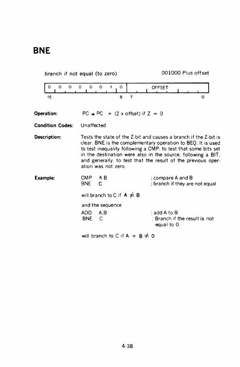
BNE
branch if not equal (to zero) 001000 Plus offset
lo o o o o o OFFSET I
15 8 7 0
Operation: PC • PC + (2 x offset) if Z 0
Condition Codes: Unaffected
Description: Tests the state of the Z-bit and causes a branch if the Z-bit is clear. BNE is the complementary operation to BEQ. It is used to test inequality following a CMP, to test that some bits set in the destination were also in the source, following a BIT, and generally, to test that the result of the previous operation was not zero.
Example: CMP A B BNE C
will branch to C if A -F B
and the sequence
ADD A,B BNE C
; compare A and B : branch if they are not equal
:add A to B : Branch if the result is not
equal to 0
will branch to C if A + B-::/::- 0
4-38

branch if equal (to zero)
15
0 0 0 I
8 7
Operation: PC ~ PC + (2 x offset) if
Condition Codes: Unaffected
BEQ
001400 Plus offset
OFFSET
0
z
Description: Tests the state of the Z-bit and causes a branch if Z is set As an example, it is used to test equality following a CMP operation, to test that no bits set in the destination were also set in the source following a BIT operation, and generally, to test that the result of the previous operation was zero.
Example: CMP A,B SEQ C
will branch to C if A = 8 and the sequence
ADD A.B SEQ C
; compare A and 8 ; branch if they are equal
(A- 8 = 0)
; add A to 8 ; branch if the result=O
will branch to C if A + 8 = 0.
4-39

BPL
branch if plus 100000 Plus offset
,, I 0
15
Operation:
Description:
0 0 0 0 I o I o
8
OFFSET
7
PC • PC + (2 x offset) if N =0
0
Tests the state of the N-bit and causes a branch if N is clear, (positive result).
4-40
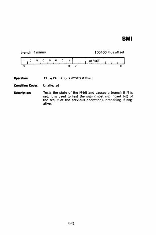
BMI
branch if minus 100400 Plus offset
I t I 0 0 0 I 0 0 0 OFFSET
t5 8 7 0
Operation: PC • PC + (2 x offset) if N = 1
Condition Codes: Unaffected
Description: Tests the state of the N·bit and causes a branch if N is set. It is used to test the sign (most significant bit) of the result of the previous operation), branching if neg· ative.
4·41

BVC
branch if overflow is clear 102000 Plus offset
l' I 0 0
15
Operation:
Dasc:ri ption:
o I o 0 I 0 I OFFSET
8 7 0
PC • PC + (2 x offset) if v-o
Tests the state of the V bit and causes a branch if the V bit is clear. BVC is complementary operation to BVS.
4-42
BVS
branch if overflow is set 102400 Plus offset
0 0 0 0 I
0 OFFSET
15
Operation:
Description:
8 7 0
PC • PC + (2 x offset) if V = 1
Tests the state of V bit (overflow) and causes a branch if the V bit is set. BVS is used to detect arithmetic overflow in the previous operation.
4-43

BCC
branch if carry is clear 103000 Plus offset
,, I o 0
15
Operation:
Description:
0 I 0 1 I o OFFSET
8 7 0
PC • PC + (2 x offset) if C =0
Tests the state of the C-bit and causes a branch if C is clear. BCC is the complementary operation to BCS
4-44

BCS
branch if carry is set 103400 Plus offset
11 0
15
Operation:
Description:
0 0 0 OFFSET I
8 7 0
PC • PC + (2 x offset) if C=l
Tests the state of the C-bit and causes a branch if C is set. It is used to test for a carry in the result of a previous operation.
4-45
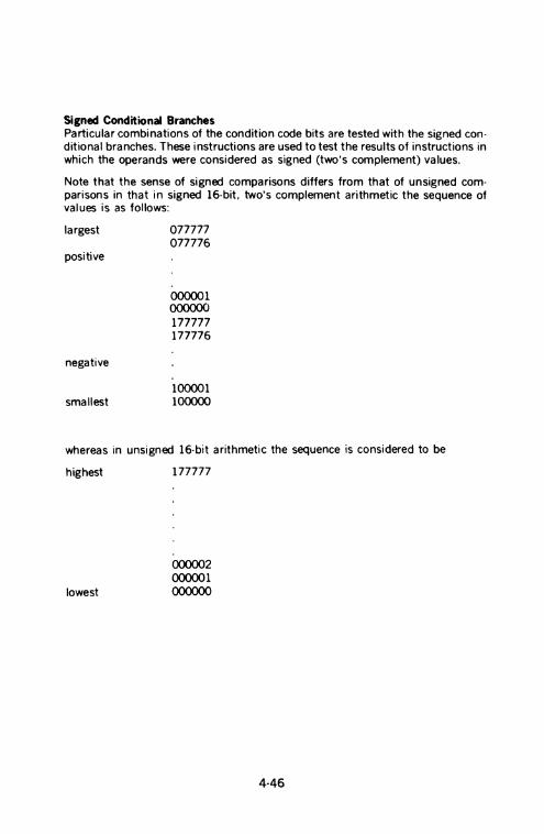
Signed Conditional Branches Particular combinations of the condition code bits are tested with the signed conditional branches. These instructions are used to test the results of instructions in which the operands were considered as signed (two's complement) values.
Note that the sense of signed comparisons differs from that of unsigned com· parisons in that in signed 16-bit, two's complement arithmetic the sequence of values is as follows:
largest
positive
negative
smallest
077777 077776
000001 000000 177777 177776
100001 100000
whereas in unsigned 16-bit arithmetic the sequence is considered to be
highest
lowest
177777
000002 000001 ()()()()()()
4·46

BGE
branch if greater than or equal (to zero)
002000 Plus offset
15
Operation:
Description:
OFFSET
8 7 0
PC -. PC + (2 x offset) if N v V = 0
Causes a branch if Nand V are either both clear or both set. BGE is the complementary operation to BLT. Thus BGE will always cause a branch when it follows an operation that caused addition of two positive numbers. BGE will also cause a branch on a zero result.
4-47

BLT
branch if less than (zero) 002400 Plus offset
o I o 0
15
Operation:
Description:
o I o OFFSET I
8 7 0
PC • PC + (2 x offset) if N ..,. V = 1
Causes a branch if the "Exclusive Or"of theN and V bits are 1. Thus BLT will always branch following an operation that added two negative numbers, even if overflow occurred. In particular, Bl T will always cause a· branch if it follows a CMP instruction operating on a negative source and a posi· tive destination (even if overflow occurred). Further, BL T will never cause a branch when it follows a CMP instruction operating on a positive source and negative destination. Bl T will not cause a branch if the result of the previous operation was zero (without overflow).
4·48
BGT
branch if greater than (zero) 003000 Plus offset
I 0 I 0 0 0 I 0 OFFSET
15
Operation:
Description:
8 7 0
PC -. PC + (2 x offset) if Z v(N \0 V) = 0
Operation of BGT is similar to BGE, except BGT will not cause a branch on a zero result
4-49

BLE
branch if less than or equal (to zero) 003400 Plus offset
I 0 I 0 0 0 0 OFFSET
15
Operation:
Description:
8 7 0
PC • PC + (2 x offset) if Z v(N v- V) = 1
Operation is similar to BL T but in addition will cause a branch if the result of the previous operation was zero.
4-50

Unsigned Conditional Branches The Unsigned Conditional Branches provide a means for testing the result of comparison operations in which the operands are considered as unsigned values.
4·51

BHI
branch if higher 101000 Plus offset
15
Operation:
Description:
OFFSET I
8 7 0
PC • PC + (2 x offset) if C = 0 and Z = 0
Causes a branch if the previous operation caused neither a carry nor a zero result. This will happen in comparison (CMP) operations as long as the source has a higher unsigned value than the destination.
4·52

BLOS
branch if lower or same 101400 Plus offset
15
Operation:
Description:
OFFSET
8 7 0
PC -. PC + (2 x offset) if C v Z = 1
Causes a branch if the previous operation caused either a carry or a zero result. BLOS is the complementary operation to BHI. The branch will occur in comparison operations as long as the source is equal to, or has a lower unsigned value than the destination.
4-53

BHIS
branch if higher or same 103000 Plus offset
1 , o o o o 0 OFFSET
15
Operation:
Description:
8 7 0
PC • PC + (2 x offset) if C = 0
BHIS is the same instruction as BCC. This mnemonic is in· eluded only for convenience.
4-54

BLO
branch if lower 103400 Plus offset
0 0 0 0 OFFSET
15
Operation:
Description:
8 7 0
PC-. PC + (2 x offset) if C= 1
BLO is same instruction as BCS. This mnemonic is included only for convenience.
4·55

JMP
jump 000100
I 0 I 0 0 o I o 0 d I d d d
15 6 5 0
Operation: PC.(dst)
Condition Codes: not affected
Description: JMP provides more flexible program branching than provided with the branch instructions. Control may be transferred to any location in memory (no range limitation) and can be ac· complished with the full flexibility of the addressing modes, with the exception of register mode 0. Execution of a jump with mode 0 will cause an "illegal instruction"condition. (Program control cannot be transferred to a register.) Regis· ter deferred mode is legal and will cause program control to be transferred to the address held in the specified register. Note that instructions are word data and must therefore be fetched from an even-numbered address. A 'boundary er· ror"trap condition will result when the processor attempts to fetch an instruction from an odd address.
Deferred index mode JMP instructions permit transfer of control to the address contained in a selectable element of a table of dispatch vectors.
4-56

Subroutine Instructions The subroutine call in the PDP·ll provides for automatic nesting of subroutines, reentrancy, and multiple entry points. Subroutines may call other subroutines (or indeed themselves) to any level of nesting without making special provision for storage or return addresses at each level of subroutine call. The subroutine call· ing mechanism does not modify any fixed location in memory, thus providing for nientrancy. This allows one copy of a subroutine to be shared among several in· terrupting processes. For more detailed description of subroutine programming· see Chapter 5.
4-57

JSR
jump to subroutine 004RDD
15
Operation:
Description:
9 B 6 5 0
(tmp).(dst) (tmp is an internal processor register)
t (SP).reg (push reg contents onto processor shck)
reg.PC (PC holds location following JSR; this address now put in reg)
PC.(tmp} (PC now points to subroutine destination)
In execution of the JSR, the old contents of the specified register (the "LINKAGE POINTER") are automatically pushed onto the processor stack and new linkage information placed in the register. Thus subroutines nested within subroutines to any depth may all be called with the same linkage register. There is no need either to plan the maximum depth at which any particular subroutine will be called or to include instructions in each routine to save and restore the linkage pointer. Further, since all linkages are saved in a reentrant manner on the processor stack execution of a subroutine may be interrupted, the same subroutine reentered and executed by an interrupt service routine. Execution of the initial subroutine can then be resumed when other requests are satisfied. This process (called nesting) can proceed to any level.
A subroutine called with a JSR reg,dst instruction can access the arguments following the call with either autoincrement addressing, (reg)+, (if arguments are accessed sequentially) or by indexed addressing, X(reg), (if accessed in random order). These addressing modes may also be deferred, @(reg)+ and @X(reg) if the parameters are operand ad· dresses rather than the operands themselves.
4·58
Example:
Before:
After:
JSR PC, dst is a special case of the PDP-11 subroutine call suitable for subroutine calls that transmit parameters through the general registers. The SP and the PC are the only registers that may be modified by this call.
Another special case of the JSR instruction is JSR PC, @(SP) + which exchanges the top element of the processor stack and the contents of the program counter. Use of this instruction allows two routines to swap program control and resume operation when recalled where they left off. Such rou· tines are called "co-routines."
Return from a subroutine is done by the RTS instruction. RTS reg loads the contents of reg into the PC and pops the top element of the processor stack into the specified register.
JSR R5, SBR
(PC) R7 PC Stack
(SP) R6 n DATA 0
R5 #1
R7 SBR
I~ R6 n-2 DATA 0
#1 R5 PC+2
4-59

RTS
return from subroutine 00020R
I 0 I 0 0
15
Operation:
Description:
Example:
Before:
After:
o I o 0
PC. reg reg. (SP)•
o I o 0
3 2 0
Loads contents of reg into PC and pops the top element of the processor stack into the specified register. Return from a non-reentrant subroutine is typically made through the same register that was used in its call. Thus, a subroutine called with a JSR PC, dst exits with a RTS PC and a subroutine called with a JSR RS, dst, may pick up para· nieters with addressing modes (RS) + , X(RS), or @X(RS) and finally exits, with an RTS RS
RTS R5
(PC) R7 SBR Stack
(SP) R6 ~ DATA 0
#1
R5 PC
R7 PC
R6 n+2 DATA 0
R5 #1
4-60

mark
15
Operation:
0
SP•SP+2xnn PC•R5 R54(SP) •
MARK
00 64 NN
0 n I n n
8 7 6 5 0
nn ""number of parameters
Condition Codes: unaffected
Description: Used as part of the standard PDP-11 subroutine return convention. MARK facilitates the stack clean up procedures involved in subroutine exit. Assembler format is: MARK N
Example: MOV MOV rv.ov
RS,-(SP) Pl,-(SP) P2,-(SP)
MOV PN,-(SP) MOV #MARKN,-(SP)
MOV SP ,RS
JSR PC,SUB
;place old RS on stack ;place N parameters ;on the stack to be ;used there by the :subroutine
;places the instruction ;MARK N on the stack ;set up address at Mark N instruction
;jump to subroutine
At this point the stack is as follows:
OLD R5
P1
PN
WIRKN
OLD PC
4·61

And the program is at the address SUB which is the beginning of the subroutine. SUB: ;execution of the subroutine it·
self
RTSR5 ;the return begins: this causes
the contents of R5 to be placed in the PC which then results in the execution of the instruction MARK N. The contents of old PC are placed in R5
MARK N causes: (1) the stack pointer to be adjusted to point to the old R5 value; (2) the value now in R5 (the old PC) to be placed in the PC; and (3) contents of the the old R5 to be popped into R5 thus completing the return from subroutine.
4·62

SOB
subtract one and branch iil ~ ·)) 077ROO Plus offset
0
15 9 8
r I 6 5
OFFSET I
0
Operation: R• R -1 if this result + 0 then PC • PC -(2 x offset)
Condition Codes: unaffected
Description: The register is decremented. If it is not equal to 0, twice the offset is subtracted from the PC (now pointing to the follow· ing word). The offset is interpreted as a sixbit positive num· ber. This instruction·provides a fast. efficient method of loop control. Assembler syntax is:
SOB R,A
Where A is the address to which transfer is to be made if the decremented R is not equal to 0. Note that the SOB instruc· tion can not be used to transfer control in the forward direc· tion.
4-63

Traps Trap instructions provide for calls to emulators, l/0 monitors, debugging packages, and user-defined interpreters. A trap is effectively an interrupt generated by software. When a trap occurs the contents of the current Program Counter (PC) and Program Status Word (PS) are pushed onto the processor stack and replaced by the contents of a two-word trap vector containing a new PC and new PS. The return sequence from a trap involves executing an RTI or RTT instruction which restores the old PC and old PS by popping them from the stack. Trap vectors are located at permanently assigned fixed addresses.
4-64

emulator trap
15
Operation: f {SP).PS f{SP).PC
PC-4(30} PS4(32)
8 7
Condition Codes: N: loaded from trap vector Z: loaded from trap vector V: loaded from trap vector C: loaded from trap vector
EMT
104000:_104377
0
Description: All operation codes from 104000 to 104377 are EMT instructions and may be used to transmit information to the emulat· ing routine (e.g., function to be performed). The trap vector for EMT is at address 30. The new PC is taken from the word at address 30; the new central processor status (PS) is taken from the word at address 32.
Before:
After:
Caution: EMT is used frequently by DEC system software and is therefore not recommended for general use.
PS PS 1 Stack
R7, PC
~ DATA 1
R6, SP
PS (32)
PC I {30) I DATA 1
PS 1
SP I n 4 I PC 1
4·65

TRAP
trap
, I o 0 o I 1 0
0p•ation: 't {SP)4PS 't{SP)4PC
PC.{34) PS.(36}
0 I , I 8 7
Condition Codes: N: loaded from trap vector Z: loaded from trap vector V: loaded from trap vector C: loaded from trap vector
104400-104777
0
Description: Operation codes from 104400 to 104777 are TRAP instructions. TRAPs and EMTs are identical in operation, except that the trap vector for TRAP is at address 34.
Note: Since DEC software makes frequent use of EMT, the TRAP instruction is recommended for general use.
4·66

BPT
breakpoint trap 000003
lo 1 o o o o o o 1 o:o o o o o o 1l 15 0
Operation: t (SP~PS t(SP~PC
PC""' (14) PS ""'(16)
Condition Codes: N: loaded from trap vector Z: loaded from trap vector V: loaded from trap vector C: loaded from trap vector
Description: Performs a trap sequence with a trap vector address of 14. Used to call debugging aids. The user is cautioned against employing code 000003 in programs run under these de· bugging aids. (no information is transmitted in the low byte.)
4·67

lOT
input/output trap 000004
0 0 o I o 0 0 0 o o 1 15 0
Operation: f(SP).PS f(SP).PC
PC4(20) PS4(22)
Condition Codes: N:loaded from trap vector Z:loaded from trap vector V:loaded from trap vector C:loaded from trap vector
Description: Performs a trap sequence with a trap vector address of 20. Used to call the 1/0 Executive routine lOX in the paper tape software system, and for error reporting in the Disk Operating System. (no information is transmitted in the low byte)
4-68

RTI
return from interrupt 000002
1 o o o
15
Operation:
Condition Codes:
Description:
PC.tCSP~ PS•(SP).t
0 0 0 0 I
N: loaded from processor stack Z: loaded from processor stack V: loaded from processor stack C: loaded from processor stack
0
Used to exit from an interrupt or TRAP service routine. The PC and PS are restored (popped) from the processor stack.
4-69

RTT
return from interrupt 000006
0 0 0 0 0 0 o,o:o 0 0 0 0 0
15 0
Operation: flC..t(SP) • PS•(SP) •
Condition Codes: N: loaded from processor stack Z: loaded from processor stack V: loaded from processor stack C: loaded from processor stack
Description: This is the same as the RTI instruction except that it inhibits a trace trap, while RTI permits a trace trap. If a trace trap is pending, the first instruction after the RTT will be executed prior to the next "T"trap. In the case of the RTI instruction the "T" trap will occur immediately after the RTI.
4-70
Reserved Instruction Traps- These are caused by attempts to execute instruction codes reserved for future processor expansion (reserved instructions) or instructions with illegal addressing modes (illegal instructions). Order codes not corresponding to any of the instructions described are considered to be reserved instructions. JMP and JSR with register mode destinations are illegal instructions. Reserved and illegal instruction traps occur as described under EMT, but trap through vectors at addresses 10 and 4 respi3Ctively.
Stack Overflow Trap Bus Error Traps - Bus Error Traps are:
1. Boundary Errors - attempts to reference instructions or word operands at odd addresses.
2. Time-Out Errors - attempts to reference addresses on the bus that made no response within15JLS in the PDP-11/40. In general, these are caused by attempts to reference non-existent memory, and attempts to reference non-existent peripheral devices.
Bus error traps cause processor traps through the trap vector address 4.
Trace Trap - Trace Trap enables bit 4 of the PS and causes processor traps at the end of instruction executions. The instruction that is executed after the instruction that set the T-bit will proceed to completion and then cause a processor trap through the trap vector at address 14. Note that the trace trap is a system debugging aid and is transparent to the general programmer.
The following are special cases and are detailed in subsequent paragraphs.
1. The traced instruction cleared the T-bit
2. The traced instruction set the T-bit.
3. The traced instruction caused an instruction trap.
4. The traced instruction caused a bus error trap.
5. The traced instruction caused a stack overflow trap.
6. The process was interrupted between the time the T-bit was set and the fetching of the instruction that was to be traced.
7. The traced instruction W<IS a WAIT.
8. The traced instruction was a HALT.
9. The traced instruction was a Return from Trap
Note: The traced instruction is the instruction after the one that sets the T-bit
An instruction that cleared the T-bit · Upon fetching the traced instruction an in· temal flag, the trace flag, was set The trap will still occur at the end of execution of this instruction. The stacked status word. however, will have a clear T-bit
An instruction that set the T-bit ·Since the T-bit was already set, setting it again has no effect The trap will occur.
4-71

An instruction that caused an Instruction Trap· The instruction trap is sprung and the entire routine for the service trap is executed. If the service routine exists with an RTI or in any other way restores the stacked status word, the T-bit is set again, the instruction following the traced instruction is executed and, unless it is one of the special cases noted above, a trace trap occurs.
An instruction that caused a Bus Error Trap · This is treated as an Instruction Trap. The only difference is that the error service is not as likely to exit with an RTI, so that the trace trap may not occur.
An instruction that caused a stack overflow· The instruction completes execution as usual · the Stack Overflow does not cause a trap. The Trace Trap Vector is loaded into the PC and PS, and the old PC and PS are pushed onto the stack. Stack Overflow occurs again, and this time the trap is made.
An interrupt between setting of the T-bit and fetch of the traced instruction ·The entire interrupt service routine is executed and then the T-bit is set again by the exiting RTI. The traced instruction is executed (if there have been no other inter· rupts) and, unless it is a special case noted above, causes a trace trap.
Note that interrupts may be acknowledged immediately after the loading of the new PC and PS at the trap vector location. To lock out all interrupts, thll PS at the trap vector should raise the processor priority to level 7.
A WAIT· The trap occurs immediately.
A HALT · The processor halts. When the continue key on the console is pressed, the instruction following the HALT is fetched and executed. Unless it is one of the exceptions noted above, the trap occurs immediately following execution.
A Return from Trap · The return from trap instruction either clears or sets the T bit. It inhibits the trace trap. If the T·bit was set and RTT is the traced instruction the trap is delayed until completion of the next instruction.
Power Failure Trap· is a standard PDP-11 feature. Trap occurs whenever the AC power drops below 95 volts or outside 47 to 63 Hertz. Two milliseconds are then allowed for power down processing. Trap vector for power failure is at locations 24 and 26.
Trap priorities . in case multiple processor trap conditions occur simultaneously the following order of priorities is observed (from high to low):
Odd Address Fatal Stack Violation Memory Management Violation Timeout Trap Instructions Trace Trap Warning Stack Violation Power Failure
The details on the trace trap process have been described in the trace trap oper· ational description which includes cases in which an instruction being traced causes a bus error, instruction trap, or a stack overflow trap.
4-72

If a bus error is caused by the trap process handling instruction traps, trace traps, stack overflow traps, or a previous bus error, the processor is halted.
If a stack overflow is caused by the trap process in handling bus errors, instruc· tion traps, or trace traps, the process is completed and then the stack overflow trap is sprung.
4-73

4. 7 MISCELLANEOUS
HALT
halt
1!5
0 0 I
Condition Cod•: not affected
0 0 0 I
0
000000
0
Description: Causes the processor operation to cease. The console is given control of the bus. The console data lights display the contents of RO; the console address lights display the ad· dress after the halt instruction. Transfers on the UNIBUS are terminated immediately. The PC points to the next instruc· tion to be executed. Pressing the continue key on the console causes processor operation to resume. No !NIT signal is given.
Note: A halt issued in User Mode will generate a trap.
4·74

WAIT
wait for interrupt 000001
jo 1 o o o o o o o:o o o o o o o , I m o
Condition Codes: not affected
Description: Provides a way for the processor to relinquish use of the bus while it waits for an external interrupt. Having been given a WAIT command, the processor will not compete for bus use by fetching instructions or operands from memory. This permits higher trans· fer rates between a device and memory, since no processor-induced latencies will be encountered by bus requests from the device. In WAIT, as in all in· structions, the PC points to the next instruction fol· lowing the WAIT operation. Thus when an interrupt causes the PC and PS to be pushed onto the pro· cessor stack, the address of the next instruction following the WAIT is saved. The exit from the in· terrupt routine (i.e. execution of an RTI instruction) will cause resumption of the interrupted process at the instruction following the WAIT.
4-75

RESET
reset external bus 000005
I 0 I 0 0 0 0 0 0 0 : 0 0 0 0 0 o , 1
~ 0
Condition Codes: not affected
Description: Sends IN IT on the UNIBUS for 10 ms. All devices on the UNI· BUS are reset to their state at power up.
4·76

(Memory Management option) M fPI
move from previous instruction space 0065SS
5 I 5
6 5 0
Operation: (temp) • (src)
• (SP).(temp)
Condition Codes: N: set if the source <0; otherwise cleared Z: set if the source = 0; otherwise cleared V: cleared
Description:
C: unaffected
This instruction is provided in order to allow inter· address space communication when the PDP-11/40 is using the Memory Management unit. The address of the source operand is determined in the current address space. That is, the address is determined using the SP and memory segments determined by PS (bits 15, 14). The address itself is then used in the previous mode (as determined by PS (bits 13, 12) to get the source operand). This operand is then pushed on to the current R6 stack.
4·77

MTPI (Memory Management option)
move to previous instruction space
15 6 5
Operation: (temo'\.t(SPV· (dst).(temp')
Condition Codes: N: set if the source <0; otherwise cleared
Z: set if the source = 0; otherwise cleared V: cleared
C: unaffected
0066DD
0
Description: The address of the destination operand is determined in the current address space. MTPI then pops a word off the current stack and stores that word in the destination address in the previous mode's (bits 13. 12 of PS).
4·78

Condition Code Operators CLN SEN CLZ SEZ CLV SEV CLC SEC CCC sec
condition code operators 0002XX
1 o o o o 0 0 o I o : l o I 1 lo!1[Njzjv I c I I I I I 15 5 4 3 2 0
Description: Set and clear condition code bits. Selectable combinations of these bits may be cleared or set together. Condition code bits corresponding to bits in the condition code operator (Bits 0-3) are modified according to the sense of bit 4, the set/clear bit of the operator. i.e. set the bit specified by bit 0, 1, 2 or 3, if bit 4 is a 1. Clear corresponding bits if bit 4 = 0.
Mnemonic Operation
CLC Clear C
CLV Clear V
CLZ Clear Z
CLN Clear N
SEC SetC
SEV Set V
SEZ Set Z
SEN Set N
sec Set all CC's
CCC Clear all CC's
ClearV and C
NOP No Operation
OP Code
000241
000242
000244
000250
000261
000262
000264
000270
000277
000257
000243 000240
Combinations of the above set or clear operations may be ORed together to form combined instructions.
4-79


CHAPTER 5
PROGRAMMING TECHNIQUES
In order to produce programs which fully utilize the power and flexibility of the PDP-11, the reader should become familiar with the various programming techniques which are part of the basic design philosophy of the PDP-11. Although it is possible to program the PDP-11 along traditional lines such as "accumulator orientation" this approach does not fully exploit the architecture and instruction set of the POP-11.
5.1 THE STACK A "stack", as used on the PDP-11. is an area of memory set aside by the programmer for temporary storage or subroutine/interrupt service linkage. The instructions which facilitate "stack" handling are useful features not normally found in low-cost computers. They allow a program to dynamically establish, modify, or delete a stack and items on it. The stack uses the "last-in, first-out" COI'\Cept, that is, various items may be added to a stack in sequential order ~nd retrieved or deleted from the stack in reverse order. On the PDP-11, a stack starts at the highest location reserved for it and expands linearly downward to the lowest address as items are added to the stack.
HIGH ADDRESSES
LOW ADDRESSES
Figure 5-1: Stack Addresses
The programmer does not need to keep track of the actual locations his data is being stacked into. This is done automatically through a "stack pointer." To keep track of the last item added to the stack (or "where we are" in the stack) a General Register always contains the memory address where the last item is stored in the staek. In the PDP-11 any register except Register 7 (the Program Counter-PC) may be used as a "stack pointer" under program control; however, instructions associated with subroutine linkage and interrupt service automatically use Register 6 (R6) as a hardware "Stack Pointer." For this reason R6 is frequently referred to as the system "SP."
5·1

Stacks in the PDP-11 may be maintained in either full word or byte units. This is true for a stack pointed to by any register except R6, which must be organized in full word units only.
WORD STACK
ITEM #1
ITEM #2
ITEM #3
007100
007076
007074
007072
007070
007066
007064
I--IT_E_M_*_4_--1- sP IL ___ oo_7_o_7_z _ _,
007100
007077
007076
007075
BYTE STACK
ITEM ... , ITEM #2
ITEM #3
ITEM #4
NOTE: BYTES ARE ARE ARRANGED IN WORDS AS FOLLOWING:
---sPl L ___ o_o7_o_7_5 __ ~
Figure 5-2: Word and Byte Stacks
Items are added to a stack using the autodecrement addressing mode with the appropriate pointer register. (See Chapter 3 for description of the autoincrement!decrement modes).
This operation is accomplished as follows;
MOV Source,-(SP) ;MOV Source Word onto the stack
or
MOVB Source,-(SP) ;MOVB Source Byte onto the stack
This is called a "push" because data is "pushed onto the stack."
5-2
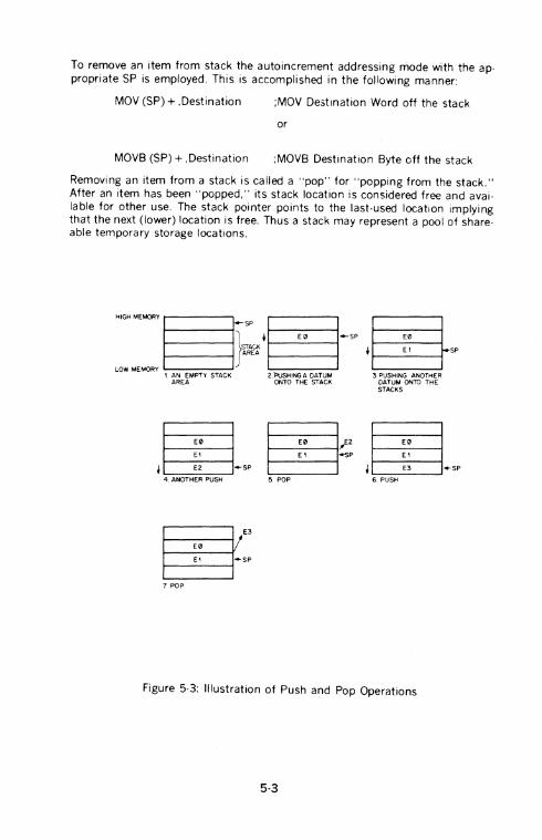
To remove an item from stack the autoincrement addressing mode with the appropriate SP is employed. This IS accomplished in the following manner:
MOV (SP) +.Destination ;MOV Destination Word off the stack
or
MOVB (SP) +.Destination ;MOVB Dest1nation Byte off the stack
Removing an item from a stack is called a "pop" for "popping from the stack." After an item has been "popped," its stack location is considered free and available for other use. The stack po1nter points to the last-used locat1on implying that the next (lower) location is free. Thus a stack may represent a pool of shareable temporary storage locations.
HIGHMEMORY~ ~ +-SP
} I E0 +-SP
STACK AREA
LOW MEMORY • 1 AN EMPTY STACK 2. PUSHING A DATUM
AREA ONTO THE STACK
~~~t 4_ ANOTHER PUSH 5. POP
7 POP
Ed j~SP
3 PUSHING ANOTHER DATUM ON1D THE STACKS
,~ ... 6 PUSH
Figure 5-3: Illustration of Push and Pop Operations
5-3

As an example of stack usage consider this situation: a subroutine (SUBR) wants to use registers 1 and 2, but these registers must be returned to the calling program with their contents unchanged. The subroutine could be written as follows:
Address
076322 076324 076326 076330
076410 076412 076414 076416 076420 076422 076424
1 ndex Constants
Octal Code
010167 000074 010267 000072
016701 000006 016702 000002 000207 000000 000000
SUBR:
Assembler Syntax
MOV R1,TEMP1 ;save R1
MOV R2,TEMP2 ;save R2
MOV TEMPI. R1 ;Restore R1
MOV TEMP2, R2 ;Restore R2
RTSPC TEMP1: 0 TEMP2: 0
Figure 5-4: Register Saving Without the Stack
OR: Using the Stack
Address
010020 010022
010130 010132 010134
Octal Code
010143 SUBR: 010243
012301 012302 000207
Assembler Syntax
MOV R1, -(R3) ;push R1 MOV R2, -(R3) ;push R2
MOV (R3) +, R2 ;pop R2 MOV (B3) +, R1 ;pop R1 RTSPC
Note: In this case R3 was used as a Stack Pointer
Figure 5-5: Register Saving using the Stack
The second routine uses four less words of instruction code and two words of temporary "stack" storage. Another routine could use the same stack space at some later point. Thus, the ability to share temporary storage in the form of a stack is a very economical way to save on memory usage.
5-4

As a further example of stack usage, consider the task of managing an input buffer from a terminal. As characters come in, the termtnal user may wish to delete characters from his line; this is aceomplished very easily by maintaining a byte stack containing the input characters. Whenever a backspace is received a character is "popped" off the stack and eliminated from consideration. In this example, a programmer has the choice of "popping" characters to be eliminated by using either the MOVB (MOVE BYTE) or INC (INCREMENT) instructions.
001011
001010
001007
001006
00!005
001004
001003
001002
001001
c c u u
5 INC R3 5
T T
0 0
M M
E E
R R 001002
z 001001
Figure 5-6: Byte Stack used as a Character Buffpr
NOTE that in this case using the increment instruction (INC) is preferable to MOVB since it would accomplish the task of eliminating the unwanted character from the stack by readjusting the stack pointer without the need for a destination location. Also, the stack pointer (SP) used in this example cannot be the system stack pointer (R6) because R6 may only point to word (even) locations.
5.2 SUBROUTINE LINKAGE 5.2.1 Subroutine Calls Subroutines provide a facility for maintaining a single copy of a given routine which can be used in a repetitive manner by other programs located anywhere else in memory. In order to provide this facility, generalized linkage methods must be established for the purpose of control transfer and information exchange between subroutines and calling programs. The POP-11 instruction set contains several useful instructions for this purpose.
PDP-11 subroutines are called by using the JSR instruction which has the following format.
a general register (R) for linkage ----, JSR R,SUBR
an entry location (SUBR) for the subroutine ....J
5-5

When a JSR is executed, the contents of the linkage register are saved on the system R6 stack as if a MOV reg,-(SP) had been performed. Then the same register is loaded with the memory address following the JSR instruction (the contents of the current PC) and a jump is made to the entry location specified.
BEFORE
(R5l= 000132 (R6)=001776
(PC):(R7) = 001000
002000
Address Assembler Syntax Octal Code
001000 JSRR5 .SUBR 004567 001002 tndelC constant for SUBR 000064
001064 SUBR MOVA.B Olnnmm
Figure 5-7: JSR using R5
AFTER
(R5)=001004 (R6)=001774
(PC).,(R7)•001064
002000 nnnnnn
001776 r-----1_ SP r--00-17_7_6_,, 001776 r------1 001774
001772
001774 000132 .... SP 001112 r--'-'-'--'c:,_--1
001774
Figure 5-8: JSR
Note that the instruction JSR R6,SUBR is not normally considered to be a meaningful combination.
5.2.2 Argument Transmission The memory location pointed to by the linkage register of the JSR instruction may contain arguments or addressses of arguments. These arguments may be accessed from the subroutine in several ways. Using Register 5 as the linkage register, the first argument could be obtained by using the addressing modes indicated by (R5), (R5) + ,X(R5) for actual data, or @(R5) +,etc. for the address of data. If the autoincrement mode is used, the linkage register is automatically updated to point to the next argument.
Figures 5-9 and 5-10 illustrate two possible methods of argument transmission.
Address Instructions and Data
010400 010402
010404 010406
020306 SU BR: 020310
JSR R5,SUBR Index constant for SUBR arg #1 arg #2
MOV (R5) + ,R1 MOV (R5) + ,R2
SUBROUTINE CALL
ARGUMENTS
;get arg # 1 ;get arg # 2 Retrieve Arguments from SUB
Figure 5-9; Argument Transmission -Register Autoincrement Mode
5-6

Address Instructions and Data
010400 JSR R5,SUBR 010402 index constant for SUBR SUBROUTINE CALL 010404 077722 Address of Arg # 1 Olo4o6 077724 Address of Arg. # 2 010410 077726 Address of Arg. # 3
077722 Arg # 1 077724 arg #2 arguments 077726 arg #3
020306 SUBR: MOV @(R5)+,R1 ;get arg # 1 020301 MOV @(R5) + ,R2 ;get arg #2
Figure 5-10: Argument Transmission-Register Autoincrement Deferred Mode
Another method of transmitting arguments is to transmit only the address of the first item by placing this address in a general purpose register. It is not necessary to have the actual argument list in the same general area as the subroutine call. Thus a subroutine can be called to work on data located anywhere in memory. In fact, in many cases, the operations performed by the subroutine can be applied directly to the data located on or pointed to by a stack without the need to ever actually move this data into the subroutine area.
Calling Program: MOV JSR
SUBROUTINE ADD
POINTER, R1 PC,SUBR
(R1) + ,(R1) ;Add item # 1 to item #2, place result in item #2, R1 points
etc. or
to item # 2 now
ADD (R1),2(R1) ;Same effect as above except that
R1 still points to item # 1 etc.
ITEM #t -Rt I ITEM # 2 '------'
Figure 5-11: Transmitting Stacks as Arguments
5-7

Because the PDP-11 hardware already uses general purpose register R6 to point to. a stack for saving and restoring PC and PS (processor status word) information, it is quite convenient to use this same stack to save and restore intermediate results and to transmit arguments to and from subroutines. Using R6 in this manner permits extreme flexibility in nesting subroutines and interrupt service routines.
Since arguments may be obtained from the stack by using some form of register indexed addressing, it is sometimes useful to save a temporary copy of R6 in some other register which has already been saved at the beginning of a subroutine. In the previous example R5 may be used to index the arguments while R6 is free to be incremented and decremented in the course of being used as a stack pointer. If R6 had been used directly as the base for indexing and not "copied", it might be difficult to keep track of the position in the argument list since the base of the stack would change with every autoincrement/decrement which occurs.
oro #1 O'Q ... arg #2 or; # 2
SP-+ org #3 oro #3
oro# 2 Is ot source -2 (SPl
but when another item TO is pushed
TO
oro#2 Is at source -4(SPJ
Figure 5-12: Shifting Indexed Base
However, if the contents of R6 (SP) are saved in R5 before any arguments are pushed onto the stack, the position relative to R5 would remain const<>nt.
1---o'..:.Q--:'"--:'--;-R!i SP org #2
erg #I - org # 2
SP- erg #3
org#2 1sot 2(R5l aro#21s stlllot2{R5l
Figure 5-13: Constant Index Base Using "R6 Copy"
5·8

5.2.3 Subroutine Return In order to provide for a return from a subroutine to the calling program an RTS instruction is executed by the subroutine. This instruction should specify the same register as the JSR used in the subroutine call. When executed, it causes the register specified to be moved to the PC and the top of the stack to be then placed in the register specified. Note that if an RTS PC is executed, it has the effect of returning to the address specified on the top of the stack.
Note that the JSR and the JMP Instructions differ in that a linkage register is al· ways used with a JSR; there is no linkage register with a JMP and no way to return to the calling program.
When a subroutine finishes, it is necessary to "clean-up" the stack by eliminating or skipping over the subroutine arguments. One way this can be done is by insist· ing that the subroutine keep the number of arguments as its first stack item. Returns from subroutines would then involve calculating the amount by which to reset the stack pointer, resetting the stack pointer, then restoring the original contents of the register which was used as the copy of the stack pointer. The PDP· 11140, however, has a much faster and simpler method of performing these tasks. The MARK instruction which is stored on a stack in place of "number of argument" information may be used to automatically perform these "clean-up" chores.
5.2.4 PDP·ll Subroutine Advantages There are several advantages to the PDP-11 subroutine calling procedure.
a. arguments can be quickly passed between the calling program and the subroutine.
b. if the user has no arguments or the arguments are in a general register or on the stack the JSR PC,DST mode can be used so that none of the general purpose registers are taken up for linkage.
c. many JSR's can be executed without the need to provide any saving procedure for the linkage information since all linkage information is automatically pushed onto the stack in sequential order. Returns can simply be made by automatically popping this information from the stack in the opposite order of the JSR's.
Such linkage address bookkeeping is called automatic "nesting" of subroutine calls. This feature enables the programmer to construct fast, efficient linkages in a simple, flexible manner. It even permits a routine to call itself in those cases where this is meaningful. OtherTamifications will appear after we examine the PDP-11 interrrupt procedures.
5.3 INTERRUPTS 5.3.1 General Principles Interrupts are in many respects very similar to subroutine calls. However, they are forced, rather than controlled, transfers of program execution occurring because of some external and program-independent event (such as a stroke on the tele· printer keyboard). Like subroutines, interrupts have linkage information such
5·9

that a return to the interrupted program can be made. More information is ac· tually necessary for an interrupt transfer than a subroutine transfer because of the random nature of interrupts. The complete machine state of the program im· mediately prior to the occurrence of the interrupt must be preserved in order to return to the program without any noticeable effects. (i.e. was the previous oper· ation zero or negative, etc.) This information is stored in the Processor Status Word (PS). Upon interrupt, the contents of the Program Counter (PC) (address of next instruction) and the PS are automatically pushed onto the R6 system stack. The effect is the same as if:
MOV PS ,-(SP) MOV R7,-(SP)
had been executed.
; Push PS ; Push PC
The new contents of the PC and PS are loaded from two preassigned consecutive memory locations which are called an "interrupt vector". The actual locations are chosen by the device interface designer and are located in low memory addresses of Kernel virtual space (see interrupt vector list, Appendix 8). The first word con· tains the interrupt service routine address (the address of the new program se· quence) and the second word contains the new PS which will determine the rna· chine status including the operational mode and register set to be used by the interrupt service routine. The contents of the interrupt service vector are set un· der program control.
After the interrupt service routine has been completed, an RTI (return from inter· rupt) is performed. The two top words of the stack an! automatically "popped" and placed in the PC and PS respectively, thus resuming the interrupted pro· gram.
5.3.2 Nesting Interrupts can be nested in much the same manner that subroutines are nested. In fact, it is possible to nest any arbitrary mixture of subroutines and interrupts without any confusion. By using the RTI and RTS instructions, respectively, the proper returns are automatic.
1. Process 0 is running; SP is pointing to loca· tion PO.
2. Interrupt stops process 0 with PC= PCO, and status = PS 0 ;starts process 1.
5-10
PO§ PSO SP~ PCO

3. Process 1 uses stack for
temporary storage (TEO, TEl). PO
0
4. Process 1 interrupted with PC= PCl Po
and status = PSl; process 2 is started
5. Process 2 is running and does a JSR R?,A to Subroutine A with PC = PC2.
6. Subroutine A is runmng and uses stack for temporary storage.
5-11
SP~
PO
0
PO
1--:::PS:::0--1
PCO
TEO
.___ __ __J
PSO
PC 0
TEO
TE 1
PS 1
PC 1
PSO
PCO
TEO
TE 1
P$1
PC 1
PC2
PSO
PCO
TEO
TE1
PS 1
PC1
PC2
TA1
TA2

7. Subroutine A releases the temporary
storage holding TAl and TA2.
8. Subroutine A returns control to process 2 with an RTS R7,PC is reset to PC2.
9. Process 2 completes with an RTI instruction (dismisses interrupt) PC is reset to PC(l) and status is reset to PSl; process 1 resumes.
10. Process 1 releases the temporary
storage holding TEO and TEl.
11. Process 1 completes its operation with an RTI PC is reset to PCO and status is reset to PSO.
PO
PSO
PCO
TEO
TE1
PS1
PC1
PC2
0
PO
PSO
PCO
TEO
TE1
PS1
PC 1
POl-----l PSO
PCO
TEO
SP----+ TE1
ol-___ __J
PO~ PSO
SP~ PCO
Figure 5-14: Nested Interrupt Service Routines and Subroutines
Note that the area of interrupt service programming is intimately involved with the concept of CPU and device priority levels.
5-12

5.4 REENTRANCY Further advantages of stack organization become apparent in complex situations which can arise in program systems that are engaged in the concurrent handling of several tasks. Such multi-task program environments may range from relatively simple single-user applications which must manage an intermix of 1!0 interrupt service and background computation to large complex multi-programming systems which manage a very intricate mixture of executive and multi-user programming situations. In all these applications there is a need for flexibility and time/memory economy. The use of the stack provides this economy and flexibility by providing a method for allowing many tasks to use a single copy of the same routine and a simple, unambiguous method for keeping track of com· plex program linkages.
The ability to share a single copy of a given program among users or tasks is called reentrancy. Reentrant program routines <!iffer from ordinary subroutines in that it is unnecessary for reentrant routines to finish processing a given task be· fore they can be used by another task. Multiple tasks can be in various stages of completion in the same routine at any time. Thus the following situation may oc· cur:
MEMORY
""OGRAM1~ PROGRAM 2 SUBRCXJTINE A F'ROGAAM3
PDP-11 Approach
Programs 1, 2, and 3 can share Subroutine A.
MEMOR.,.
PROGRAM 1 SUEiROUTINE A
""0GRAM 2 ~.SUBROUTINE .~
""0GRAM 3 ~~UBROUTJ~~- ~}!<
Conventional Approach
A separate copy of Subroutine A must be provided for each program.
Figure 5-15: Reentrant Routines
The chief programming distinction between a non-shareable routine and a reentrant routine is that the reentrant routine is composed solely of "pure code", i.e. it contains only instructions and constants. Thus, a section of program code is reentrant (shareable) if and only if it is "non self-modifying", that is it contains no information within it that is subject to modification.
Using reentrant routines, control of a given routine may be shared as illustrated in Figure 5-16.
5·13

REENTRANT ROUTINE
a
Figure 5-16: Reentrant Routine Sharing
1. Task A has requested processing by Reentrant Routine Q.
2. Task A temporarily relinquishes control (is interrupted) of Reentrant Routine Q before it finishes processing.
3. Task B starts processing in the same copy of Reentrant Routine Q.
4. Task B relinquishes control of Reentrant Routine Q at some point in its processing.
5. Task A regains control of Reentrant Routine Q and resumes processing from where it stopped.
The use ot reentrant programming allows many tasks to share frequently used routines such as device interrupt service routines, ASCII-Binary conversion routines, etc. In fact, in a multi-user system it is possible for instance, to construct a reentrant FORTRAN compiler which can be used as a single copy by many user programs.
As an application of reentrant (shareable) code, consider a data processing program which is interrupted while executing a ASCII-to-Binary subroutine which has been written as a reentrant routine. The same conversion ·routine is used by the deyice service routine. When the device servicing is finished, a return from interrupt (RTI) is executed and execution for the processing program is then resumed where it left off inside the same ASCII-to-Binary subroutine.
Shareable routines generally result in great memory saving. It is the hardware implemented stack facility of the PDP-11 that makes shareable or reentrant routines reasonable.
A subroutine may be reentered by a new task before its completion by the previous task as long as the new execution does not destroy any linkage information or intermediate results which belong to the previous programs. This usually amounts to saving the contents of any general purpose registers, to be used and restoring-them upon exit. The choice of whether to save and restore this information in the calling program or the subroutine is quite arbitrary and depends on the particular application. For example in controlled transfer situations (i.e. JSR's) a main program which calls a code-conversion utility might save the contents of registers which it needs and restore them after it has regained control, or the code conversion routine might save the contents of registers which it uses and re· store them upon its completion. In the case of interrupt service routines this save/restore process must be carried out by the service routine itself since the in· terrupted program has no warning of an impending interrupt. The advantage of
5·14

using the stack to save and restore (i.e. "push" and "pop") this information is that it permits a program to isolate its instructions and data and thus maintain its reentrancy.
In the case of a reentrant program which is used in a multi-programming envi· ronment it is usually necessary to maintain a separate R6 stack for each user al· though each such stack would be shared by all the tasks of a given user. For ex· ample, if a reentrant FORTRAN compiler is to be shared between many users, each time the user is changed, R6 would be set to point to a new user's stack area as illustrated in Figure 5·17.
Figure 5-17: Multiple R6 Stack
5.5 POSITION INDEPENDENT CODE · PIC Most programs are written with some direct references to specific addresses, if only as an offset from an absolute address origin. When it is desired to relocate these programs in memory, it is necessary to change the address references and/or the origin assignments. Such programs are constrained to a specifiec set of locations. However, the PDP-11 architecture permits programs to be constructed such that they are not constrained to specific locations. These Position Independent programs do not directly reference any absolute locations in memory. Instead all references are "PC-relative" i.e. locations are referenced im terms of offsets from the current location (offsets from the current value of the Program Counter (PC)). When such a program has been translated to machine code it will form a program module which can be loaded anywhere in memory as required.
Position Independent Code is exceedingly valuable for those utility routines which may be disk-resident and are subject to loading in a dynamically changing program environment. The supervisory program may load them anywhere it de· termin·es without the need for any relocation parameters since all items remain in the same positions relative to each other (and thus also to the PC).
Linkages to program routines which have been written in position independent code (PIC) must still be absolute in some manner. Since these routines can be lo· cated anywhere in memory there must be some fixed or readily locatable linkage addresses to facilitate access to these routines. This linkage address may be a simple pointer located at a fixed address or it may be a complex vector composed of numerous linkage information items.
5·15

5.6 CO.ROUTINES In some situations it happens that two program routines are highly interactive. Using a special case of the JSR instruction i.e. JSR PC,@(R6) + which exchanges the top element of the Register 6 processor stack and the contents of the Pro· gram Counter (PC), two routines may be permitted to swap program control and resume operation where they stopped, when recalled. Such routines are called "co·routines". This control swapping is illustrated in Figure 5-18.
Routine # 1 is operating, it then executes:
MOV #PC2,-(R6)
JSR PC,@(R6) + with the following results:
1) PC2 is popped from the stack
and the SP autoincremented
2) SP is autodecremented and the old PC (i.e. PC1) is pushed
3) control is transferred to the location PC2 (i.e. routine # 2)
Routine # 2 is operating, it then executes:
JSR PC ,@(R6) + with the result the PC2 is exchanged for PC1 on the stack and control is transferred back to routine # 1.
Figure 5·18 . Co-Routine Interaction
5·16

5.7 MULTI-PROGRAMMING The PDP ll/40's architecture with its two modes of operation and its Memory Management provides an ideal environment for multi-program· ming systems.
In any multi-programming system there must be some method of trans· ferring information and control between programs operating in the same or different modes. The PDP 11/40 provides the user with these com· munication paths.
5.7.1 Control Information Control is passed inwards (User to Kernel) by all traps and interrupts. All trap and interrupt vectors are located in Kernel virtual space. Thus all traps and interrupts pass through Kernel space to pick up their new PC and PS and determine the new mode of processing.
Control is passed outwards (Kernel to User) by the RTI and RTT instruc· tions.
5.7.2 Data Data is transferred between modes by two instructions: Move From Pre· vious Instruction space (MFPI) and Move To Previous Instruction space (MTPI). The instructions are fully described in Chapter 4. However, it should be noted that these instructions have been designed to allow data transfers to be under the control of the inner mode (Kernel) program and not the outer, thus providing protection of an inner program from an outer.
5.7.3 Processor Status Word The PDP 11/40 protects the PS from implicit references by User programs which could result in damage to an inner level program.
A program operating in Kernel mode can perform any manipulation of the PS. Programs operating at the outer level are inhibited from chang· ing bits 5·7 (the Processor's Priority). They are also restricted in their treatment of bits 15, 14 (Current Mode), and bits 13, 12 (Previous Mode) these bits may only be set, they are only cleared by an interrupt or trap.
Thus, a programmer can pass control outwards through the RTI and RTI instructions to set bits in the mode fields of his PS. To move inwards, however, bits must be cleared and he must therefore, issue a trap or interrupt.
The Kernel can further protect the PS from explicit references (Move data to location 777776-the PS) through Memory Management.
5-17


CHAPTER 6
MEMORY MANAGEMENT
The PDP-11/40 Memory Management Unit provides the hardware facilities necessary for complete memory management and protection. It is designed to be a memory management facility for systems where the system memory size is greater than 28K words and for multi-user, multiprogramming systems where memory protection and relocation facilities are necessary.
In order to most effectively utilize the power efficiency of the PDP· 11/40 in medium and large scale systems it is necessary to run several programs simultaneously. In such multi-programming environments several user programs would be resident in memory at any given time. The task of the supervisory program would be: control the execution of the various user programs, manage the allocation of memory and peripheral device resources, and safeguard the integrity of the system as a whole by careful control of each user program.
In a multi-programming system, the Management Unit provides the means for assigning memory pages to a user program and preventing that user from making any unauthorized access to those pages outside his assigned area. Thus, a user can effectively be prevented from accidental or willful destruction of any other user program or the system executive program.
The basic characteristics of the PDP-11/40 Memory Management Unit are:
• 8 User mode memory pages • 8 Kernel mode memory pages • 8 pages in each mode for instructions and data • page length from 32 to 4096 words • each page provided with full protection and relocation • transparent operation • 3 modes of memory access control • memory extension to 124K words (248K bytes)
6.1 PDP-11 FAMILY BASIC ADDRESSING LOGIC The addresses generated by all PDP-11 Family Central Processor Units (CPUs) are 18-bit direct byte addresses. Although the PDP-11 Family word length and operational logic is all 16-bit length, the UN I BUS and CPU addressing logic actually is 18-bit length. Thus, while the PDP-11 word can only contain address references up to 32K words (64K bytes) the CPU and UN I BUS can reference addresses up to 128K words (256K bytes). These extra two bits of addressing logic provide the basic framework for expanded memory paging.
6-1
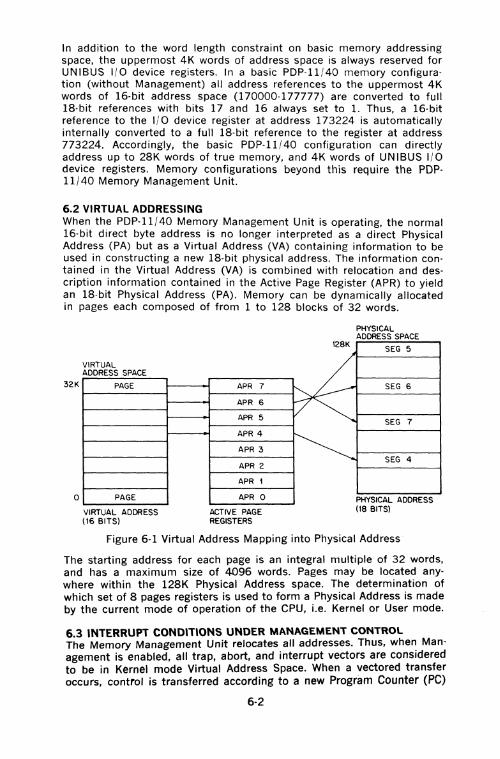
In addition to the word length constraint on basic memory addressing space, the uppermost 4K words of address space is always reserved for UNIBUS 1/0 device registers. In a basic PDP-11/40 memory configura· tion (without Management) all address references to the uppermost 4K words of 16-bit address space (170000-177777) are converted to full 18-bit reference5 with bits 17 and 16 always set to 1. Thus, a 16·bit reference to the 1/0 device register at address 173224 is automatically internally converted to a full 18-bit reference to the register at address 773224. Accordingly, the basic PDP-11/40 configuration can directly address up to 28K words of true memory, and 4K words of UNIBUS 1/0 device registers. Memory configurations beyond this require the PDP-11/40 Memory Management Unit.
6.2 VIRTUAL ADDRESSING When the PDP-11/40 Memory Management Unit is operating, the normal 16-bit direct byte address is no longer interpreted as a direct Physical Address (PA) but as a Virtual Address (VA) containing information to be used in constructing a new 18-bit physical address. The information contained in the Virtual Address (VA) is combined with relocation and description information contained in the Active Page Register (APR) to yield an 18-bit Physical Address (PA). Memory can be dynamically allocated in pages each composed of from 1 to 128 blocks of 32 words.
32K
0
VIRTUAL ADDRESS SPACE
PAGE
PAGE
VIRTUAL ADDRESS (16 SITS)
APR 7
APR 6
APR 5
APR 4
APR 3
APR 2
APR 1
APR 0
ACTIVE PAGE REGISTERS
128K
rE ~
PHYSICAL ADDRESS SPACE
SEG 5
SEG 6
SEG 7
SEG 4
PHYSICAL ADDRESS (18 BITS)
Figure 6-1 Virtual Address Mapping into Physical Address
The starting address for each page is an integral multiple of 32 words, and has a maximum size of 4096 words. Pages may be located anywhere within the 128K Physical Address space. The determination of which set of 8 pages registers is used to form a Physical Address is made by the current mode of operation of the CPU, i.e. Kernel or User mode.
6.3 INTERRUPT CONDITIONS UNDER MANAGEMENT CONTROL The Memory Management Unit relocates all addresses. Thus, when Management is enabled, all trap, abort, and interrupt vectors are considered to be in Kernel mode Virtual Address Space. When a vectored transfer occurs, control is transferred according to a new Program Counter (PC)
6-2

and Processor Status Word (PS) contained in a two-word vector relocated through the Kernel Active Page Register Set
When a trap, abort, or interrupt occurs the "push" of the old PC, old PS is to the User/ Kernel R6 stack specified by CPU mode bits 15,14 of the new PS in the vector (00 = Kernel, 11 = User)_ The CPU mode bits also determine the new APR set In this manner it is possible for a Kernel mode program to have complete control over service assignments for all interrupt conditions, since the interrupt vector is located in Kernel space. The Kernel program may assign the service of some of these conditions to a User mode program by simply setting the CPU mode bits of the new PS in the vector to return control to the appropriate mode.
6.4 CONSTRUCTION OF A PHYSICAL ADDRESS The basic information needed for the construction of a Physical Address (PA) comes from the Virtual Address (VA), which is illustrated in Figure 6-2, and the appropriate APR set.
15 13 12
APF OF
ACTIVE PAGE FIELD DISPLACEMENT FIELD
Figure 6-2 Interpretation of a Virtual Address
The Virtual Address (VA) consists of:
0
L The Active Page Field (APF). This 3-bit field determines which of eight Active Page Registers (APRO-APR7) will be used to form the Physical Address (PA).
2. The Displacement Field (DF). This 13-bit field contains an address relative to the beginning of a page. This permits page lengths up to 4K words (213 = 8K bytes). The DF is further subdivided into two fields as shown in Figure 6-3.
12 6 5 0
BN DIB
BLOCK NUMBER DISPLACEMENT IN BLOCK
Figure 6-3 Displacement Field of Virtual Address
The Displacement Field (DF) consists of:
L The Block Number (BN). This 7-bit field is interpreted as the block number within the current page_
2. The Displacement in Block (DIB). This 6-bit field contains the dis-placement within the block referred to by the Block Number.
The remainder of the information needed to construct the Physical Address comes from the 12-bit Page Address Field (PAF) (part of the Active Page Register) and specifies the starting address of the memory which that APR describes. The PAF is actually a block number in the physical memory, e.g. PAF = 3 indicates a starting address of 96, (3 x 32 = 96) words in physical memory.

The formation of a physical address takes 150 ns.
The formation of the Physical Address is illustrated in Figure 6·4.
15 13 12 6 5
I APF I BLOC!< NO I DIB J ~~~~tsLs
15 12,1~1--------~~----------~~ PAGE ADDRESS FIELD ACTIVE PAGE
L.--9 REGISTER
5 0 17
I PHYSICAL BLOCK NO 1-----1 DIB I PHYSICAL ADDRESS
(DISPLACEMENT IN BLOCK)
Figure 6·4 Construction of a Physical Address
The logical sequence involved in constructing a Physical Address is as follows:
1. Select a set of Active Page Registers depending on current mode.
2. The Active Page Field of the Virtual Address is used to select an Active Page Register (APRO-APR7).
3. The Page Address Field of the selected Active Page Register con· tains the starting address of the currently active page as a block number in physical memory.
4. The Block Number from the Virtual Address is added to the block number from the Page Address Field to yield the number of the block in physical memory which will contain the Physical Address being constructed.
5. The Displacement in Block from the Displacement Field of the Virtual Address is joined to the Physical Block Number to yield a true 18-bit PDP·ll/40 Physical Address.
6.5 MANAGEMENT REGISTERS The PDP-11/40 Memory Management Unit uses two sets of eight 32-bit Active Page Registers. An APR is actually a pair of 16-bit registers: a Page Address Register (PAR) and a Page Descriptor Register (PDR). These registers are always used as a pair and contain all the information needed to describe and locate the currently active memory pages.
One set of APR's is used in Kernel mode, and the other in User mode. The choice of which set to be used is determined by the current CPU mode contained in the Processor Status word.
The various Memory Management Registers are located in the uppermost 4K of PDP-11 physical address space along with the UNIBUS 1/0 device registers.
6·4

15 14 13
KERNAL (00)
APRO 1------1
APR 1 1--------1
APR 21--------1 APR3
1---------1 APR4 1------1 APR5
1------; APR6
1-----ooool APR7 '-------..J
PROCESSOR STATUS WORO I I
USER (11)
APRO 1------1 APR 1
1-------; APR2
1------t APR3
1-------t APR4 1------f APR5
1-----......j APR6
1-----......j APR7 '-------'
ACTIVE PAGE REGISTERS
ffi o m o ,..:I :!..-----PA-R ___ _,~-----~r'-"----PD-R ------'"--,1 PAGE ADDRESS REGISTER PAGE DESCRIPTION REGISTER
Figure 6-5 Active Page Registers
6.5.1 Page Address Registers
0
The Page Address Register is the first word of the 32-bit Active Page Register; it contains the Page Address Field, a 12-bit field, which speci· fies the starting address of the page as a block number in physical memory.
15 12 II 0
PAF
Figure 6·6 Page Address Register
Bits 15·12 of the PAR are unused and reserved for possible future use. The Page Address Register which contains the Page Address Field may be alternatively thought of as a relocation register containing a relocation constant, or as a base register containing a base address. Either interpretation indicates the basic importance of the Page Address Reg· ister as a relocation tool.
6.5.2 Page Descriptor Register The Page Descriptor Register contains information relative to page ex· pansion, length, and access control.
Figur.e 6·7 Page Descriptor Register
6·5

Access Control Field (ACF) This 2-bit field, occupying bits 2-1 of the Page Descriptor Register contains the access rights to this particular segment. The acccess codes or "keys" specify the manner in which a page may be accessed and whether or not a given access should result in an abort of the current operation. A memory reference which causes an abort is not completed. Aborts are used to catch "missing page faults," prevent illegal accesses, etc.
In the context of access control the term "write" is used to indicate the action of any instruction which modifies the contents of any addressable word. Except in those cases where references are made to the 4K word UNIBUS 1/0 register area, a "write" is synonymous with what is usually called a "store" or "modify" in many computer systems.
The modes of access control are as follows:
ACF Key Mode
00 0 non-resident abort all accesses
01 2 read only abort on write attempt
10 4 (unused) abort all accesses
11 6 read/write no system abort action
Access Information Bits W Bit (bit 6)-This bit indicates whether or not this page has been modi· fied (i.e. written into) since the PSR was loaded. (W = 1 is Affirmative) The W Bit is useful in applications which involve disk swapping and memory overlays. It is used to determine which pages have been modi· fied and hence must be saved in their new form and which pages have not been modified and can be simply overlayed.
Note that the W bit is reset to 0 whenever the Active Page Register (either PAR or PDR) is modified (written into).
Expansion Direction (ED) This one-bit field, located at bit 3 of the Page Descriptor Register, speci· fies whether the segment expands upward from relative zero (ED = 0) or downwards toward relative zero (ED = 1). Relative zero, in this case, is the PAF. Expansion is done by changing the Page Length Field. In expanding upwards, blocks with higher relative addresses are added; in expanding downwards, blocks with lower relative addresses are added to the page. Upward expansion is usually used to add more program space, while downward expansion is used to add more stack space.
Page Length Field (PLF) The seven-bit field, occupying bits 14-8 of the Page Descriptor Register, specifies the number of blocks in the page. A page consists of at least one and at most 128 blocks, and occupies contiguous core locations. If the page expands upwards, this field contains the length of the page minus one (in blocks). If the page expands downwards, this field con· tains 128 minus the length of the page (in blocks).
6-6

A Page Length Error occurs when the Block Number of the virtual address is greater than the Page Length Field, if the segment expands upwards, or if the page expands downwards, when the BN is less than the PLF.
Reserved Bits Bits 15, 4 and 5 are reserved for future use, and are always 0. Bits 7 and 0 are used by the PDP-11/45, and in the PDP-11/40 they are set to 0.
6.6 FAULT REGISTERS Aborts generated by the hardware are vectored through Kernel virtual location 250. Status Registers #0 and # 2 ( # 1 is used by the PDP-11/45) are used to determine why the abort occurred. Note that an abort to a location which is itself an invalid address will cause another abort. Thus the Kernel program must insure that Kernel Virtual Address 10 is mapped into a valid address, otherwise a loop will occur which will require console intervention.
6.6.1 Status Register #0 (SRO) (status and error indicators) SRO contains error flags, the page number whose reference caused the abort, and various other status flags. The register is organized as shown in Figure 6-8.
15 14 13 12 9 8 7 6 5 4 3 2 0
D___J.I_~==~~=--...__, ..=~C4...-.L..I --L-' _LI___J ABORT-NON RESIDENT_j J ~ '-------._.----J I ABORT -PAGE LENGTH ERROR
~8~~~~A~~~---~~~~~~~--------------~ MAINTENANCE MODE MODE PAGE NUMBER-------------------------------------------
ENABLE MANAGEMENT -------------------------------------------___j
Figure 6-8 Format of Status Register #0 (SRO)
Bits 15-13 when set (error conditions) cause Memory Management to freeze the contents of bits 1-7 and Status Register # 2.
Note that Status Register #0 (SRO) bits 0, and 8 can be set under program control to provide meaningful page control information. However, information written into all other bits is not meaningful. Only that information which is automatically written into these remaining bits as a result of hardware actions is useful as a monitor of the status of the Memory Management Unit. Setting bits 15-13 under program control will not cause traps to occur; these bits however must be reset to 0 after an abort has occurred in order to resume page status monitoring.
Abort-Non-Resident Bit 15 is the "Abort-Non-Resident" bit. It is set by attempting to access
6-7

a page with an Access Code Field key equal to 0 or 4. It is also set by attempting to use Memory Management with a mode of 1 or 2.
Abort-Page Length Bit 14 is the "Abort-Page Length" bit. It is set by attempting to access a location in a page with a block number (Virtual Address bits 12·6) that is outside the area authorized by the Page Length Field of the Ac· tive Page Register for that page. Bits 14 and 15 may be set simultane· ously by the same access attempt.
Abort-Read Only Bit 13 is the "Abort-Read Only" bit. It is set by attempting to write in a "Read·Only" page. "Read·Only" pages have an access key of 2.
Maintenance/ Designation Mode Bit 8 specifies Maintenance use of the Memory Management Unit. It is provided for diagnostic purposes only.
Mode Bits 5, 6 indicate the CPU mode (User/ Kernel) associated with the page causing the abort. (Kernel = 00, User= 11). If an illegal mode is speci· fied, management will abort and set bit 15.
Page Number Bits 3·1 contain the page number of a reference causing a fault. Note that pages, like blocks, are numbered from 0 upwards.
Enable Management Bit 0 is the "Enable Management" bit. When it is set to 1, all addresses are relocated by the Management unit. When bit 0 is set to 0 the Unit is inoperative and addresses are not relocated or protected.
6.6.2 Status Register # 2 SR2 is loaded with the 16·bit Virtual Address at the beginning of each instruction fetch. SR2 is Read·Only; it can not be written, SR2 is the Virtual Address Program Counter.
6-8

CHAPTER7
INTERNAL PROCESSOR OPTIONS
7.1 GENERAL This chapter describes 3 options which mount in the Central Processor, assembly unit. The Extended Instruction Set (EIS) option allows ex· tended manipulation of fixed point numbers. The Floating Point option (which requires the EIS option) enables direct operations on single pre· cision 32-bit words. The Stack Limit option allows dynamic adjustment of the lower boundary of permissible stack addresses.
The options are contained on individual modules that plug into dedi· cated, prewired slots.
KEll·E EIS option KEll·F Floating Point option KJll·A Stack Limit option
The basic processor timing is not degraded, and NPR latency is not affected by the use of these options.
7.2 EIS OPTION The Extended Instruction Set option adds the following instruction capability:
Mnemonic
MUL DIV ASH ASHC
Instruction
multiply divide shift arithmetically arithmetic shift combined
Op Code
070RSS 071RSS 072RSS 073RSS
The EIS instructions are directly compatible with the larger 11 computer, the PDP-11/45. The detailed operation of these instructions is covered in Chapter 4.
The number formats are: 15 14
16-bit single word: IL--s .l.I ___ ..L.-__ _.L,"_uM_~_E" _ ___._ ___ _._ __ __.I
15 14
32-bit double word: ,5 0 r,~-------~-W-NUrrM-8E_R_M_f------~~
S is the sign bit. S = 0 for positive quantities S = 1 for negative quantities; number is in 2's
complement notation
Interrupts are serviced at the end of an EIS instruction.
7·1

7-3 FLOATING POINT OPTION The Floating Point instructions used with this option are unique to the PDP-11/40. However, the Op Codes used do not conflict with any other instructions.
Mnenomic Instruction Op Code
FADD floating add 07500R FSUB floating subtract 07501R FMUL floating multiply 07502R FDIV floating divide 07503R
The number format is:
15
EXPONENT I
7 6 0
I FRACTION (HIGH PART) I . I I
HIGH ARGUMENT
0
FRACTION 11LOW PART) I I
LOW ARGUMENT
S = sign of fraction; 0 for positive, 1 for negative Exponent= 8 bits for the exponent, in excess (200), notation Fraction = 23 bits plus 1 hidden bit (all numbers are assumed to be normalized)
The number format is essentially a sign and magnitude representation. The format is identical with the 11/45 for single precision numbers.
Fraction The binary radix point is to the left (in front of bit 6 of the High Argument), so that the value of the fraction is always less than 1 in magnitude. Normalization would always cause the first bit after the radix point to be a 1, such that the fractional value would be between lh and 1. Therefore, this bit can be understood and not be represented directly, to achieve an extra 1 bit of resolution.
The first bit to the right of the radix point (hidden bit) is always a 1. The next bit for the fraction is taken from bit 6 of the High Argument. The result of a Floating Point operation is always rounded away from zero, increasing the absolute value of the number.
Exponent The 8-bit Exponent field (bits 14 to 7) allow exponent values between -128 and +127. Since an excess (200), or (128),. number system is used, the correspondence between actual values and coded representation is as follows:
Actual Value Representation
Decimal Octal Binary
+127 377 11 111 111
+1 201 10 000 001 0 200 10 000 000
·-1 177 01 111 111
-128 000 00 000 000
7-2

If the actual value of the exponent is equal to -128, meaning a total value (including the fraction) of less than 2·128, the floating point number will be assumed to be 0, regardless of the sign or fraction bits. The hard· ware will generate a clean 0 (a 32-bit word of all zeros).
Example of a Number
+(12),. = +(1100),
= +(24),. X (.11), [16 X ('lz + 1,4) = 12]
s Exponent Fraction ,....----"---.
10 000 1001 1'000000 0000000000000000
hidden bit is a 1
radix point is understood
representation: 0
Registers There are no pre-assigned registers for the Floating Point option. A general purpose register is used as a pointer to specify a stack address. The contents of the register are used to locate the operands and answer for the Floating Point operations as follows:
(R) =High 8 argument address (R)+2 = Low 8 argument address (R)+4 = High A argument;~ddress (R)+6 = Low A argument address
After the Floating Point operation, the answer is stored on the stack as follows:
(R)+4 =address for High part of answer (R)+6 = address for Low part of answer
where (R) is the original contents of the general register used.
After execution of the instruction, the general register will point to the High answer, at (R)+4.
Condition Codes Condition codes are set or cleared as shown in the Instruction Descriptions, in the next part of this section. If a trap occurs as a function of a Floating Instruction, the condition codes are re-interpreted as follows:
V = 1, if an error occurs N = 1, if underflow or divide-by-zero C = 1, if divide by zero Z=O
v Overflow 1 Underflow 1 Divide by 0 1
7-3
N c z 0 0 0 1 0 0 1 1 0

Traps occur through the vector at location 244. A Floating Point instruction will be aborted if a 8R request is issued before the instruction is within approximately 8 ~-tsec of completion. The Program Counter will point to the aborted Floating instruction so that the Interrupt will look transparent.
INSTRUCTIONS
FADD floating add
t 0 I 1 1
15
Operation:
Condition Codes:
Description:
FSUB floating subtract
I 0 I t ,
15
Operation:
Condition Codes:
Description:
0 0 I
07500R
3 2 0
[{R)+4, {R)+6] ~[(R)+4, (R)+6]+[(R),{R)+2], if result ~ 2-128; else [{R)+4, {R)+6] ~
N; set if result < 0; cleared otherwise Z: set if result = 0; cleared otherwise V: cleared C: cleared
Adds the A argument to the 8 argument and stores the result in the A Argument position on the stack. General register R is used as the stack pointer for the operation.
A~A+8
07501R
0 0 0 I
3 2 0
[(R)+4, (R)+6] ~[(R)+4, (R)+6]-[(R), (R)+2], if result ~ 2·128; else [(R)+4, (R)+6] ~
N: set if result < 0; cleared otherwise Z: set if result = 0; cleared otherwise V: cleared C: cleared
Sutracts the 8 Argument from the A Argument and stores the result in the A Argument position on the stack.
A~A-8
7·4

FMUL floating multiply 07502R
15 3 2
Operation:
Condition Codes:
Description:
FDIV floating divide
15
Operation:
Condition Codes:
Description:
[(R)+4, (R)+6J~[(R)+4, (R)+6]X[(R), (R)+2] if result ;;;::: 2-128; else [(R)+4, (R)+6] ~
N: set if result < 0; cleared otherwise Z: set if result = 0; cleared otherwise V: cleared C: cleared
Multiplies the A Argument by the 8 Argument and stores the result in the A Argument position on the stack. A~ A X 8
070503R
0 0 I I
3 2
[(R)+4, (R)+6J~[(R)+4, (R)+6] I [(R),(R)+2 J if result ;;;::: 2-128; else [(R)+4, (R)+6)] ~o
N: set if result < 0; cleared otherwise Z: set if result= 0; cleared otherwise V: cleared C: cleared
Divides the A Argument by the 8 Argument and stores the result in the A Argument position on the stack. If the divisor (8 Argument) is equal to zero, the stack is left untouched.
A~A/8
7.4 STACK LIMIT OPTION This option allows program control of the lower limit for permissible stack addresses. The limit may be varied in increments of (400), bytes or (200), words.
There is a Stack Limit Register, with the following format: 15 8 7 0
7-5

The Stack Limit Register can be addressed as a word at location 777774, or as a byte at location 777775. The register is accessible to the proces· sor and console, but not to any bus device.
The 8 bits, 15 through 8, contain the stack limit information. These bits are cleared by System Reset, Console Start, or the RESET instruction. The lower 8 bits are not used. Bit 8 corresponds to a value of (400), or (256),o.
Stack Limit Violations When instructions cause a stack address to exceed (go lower than) a limit set by the programmable Stack Limit Register, a Stack Violation occurs. There is a Yellow Zone (grace area) of 16 words below the Stack Limit which provides a warning to the program so that corrective steps can be taken. Operations that cause a Yellow Zone Violation are com· pleted, then a bus error trap is effected. The error trap, which itself uses the stack, executes without causing an additional violation, unless the stack has entered the Red Zone.
A Red Zone Violation is a Fatal Stack Error. (Odd stack or non-existent stack are the other Fatal Stack Errors.) When detected, the operation causing the error is aborted, the stack is repositioned to address 4, and a bus error occurs. The old PC and PS are pushed into locations 0 and 2, and the new PC and PS are taken from locations 4 and 6.
Stack Limit Addresses The contents of the Stack Limit Register (SL) are compared to the stack address to determine if a violation has occurred. The least significant bit of the register (bit 8) has a value of (400),. The determination of the violation zones is as follows:
Yellow Zone= (SL) + (340 through 377),
Red Zone ~ (SL) + (337),
If the Stack Limit Register contents were zero: Yellow Zone = 340 through 377 Red Zone = 000 through 337
7-6
execute, then trap
abort, then trap to IG· cation 4


CHAPTER 8
CONSOLE OPERATION
8.1 CONSOLE ELEMENTS The PDP·ll/40 Operator's Console provides the following facilities:
Power Switch (with a key lock)
ADDRESS Register display (18 bits)
DATA Register display (16 bits)
Switch Register (18 switches)
Status Lights RUN PROCESSOR BUS CONSOLE USER VIRTUAL
Control Switches LOAD ADRS (Load Address) EXAM (Examine) CONT (Continue) ENABLE/ HALT START DEP (Deposit)
8.2 STATUS INDICATORS
RUN
PROCESSOR
BUS
CONSOLE
USER
VIRTUAL
Lights when the processor clock is run· ning. It is off when the processor is wait· ing for an asynchronous peripheral data response, or during a RESET instruction. It is on during a WAIT or HALT instruction.
Lights when the processor has control of the bus.
Lights when the UNIBUS is being used.
Lights when in console mode (manual op· eration). Machine is stopped and is not executing the stored program.
Lights when the CPU is executing program instructions in User mode.
Lights when the ADDRESS Register display shows the 16-bit Virtual Address.
8-1

8.3 CONSOLE SWITCHES
POWER { OFF ON
LOCK
Switch Register ( Up = 1) (Down= 0)
Control Switches
LOAD ADRS (depress to activate)
EXAM (depress to activate)
CONT (depress to activate)
ENABLE/HALT { ENABLE
HALT
Power to the processor is off.
Power to the processor is on and all con· sole switches function normally.
Power to the processor is on, but the Con· trol Switches are disabled. The Switch Register is still functional.
Used to manually load data or an address into the processor.
Transfers contents of the Switch Register to the Bus Address register.
The resulting Bus Address is displayed in the ADDRESS Register, and provides an address for EXAM, DEP, and START. The LOAD Address is not modified during pro· gram execution. To restart a program at the previous Start Location, the START switch is activated.
Causes the contents of the location speci· tied by the Bus Address to be displayed in the DATA Register. If the EXAM switch is depressed again, the contents of the next sequential word location are displayed. (Bus Address is incremented automati· cally). If an odd address is specified, the next lower even address word will be dis· played.
Causes the processor to continue opera· tion from the point at which it had stopped. The switch has no effect when the CPU is in the RUN state. If the program had stopped, this switch provides a restart without a System Reset.
Allows the CPU to perform normal opera· tions under program control.
Causes the CPU to stop. Depressing the CONT switch will now cause execution of a single instruction.
8·2

START (depress to activate)
DEP (raise to activate)
8.4 DISPLAYS
ADDRESS Register
DATA Register
If the CPU is in the RUN state, the START switch has no effect.
If the program had stopped, depressing the START switch causes a System Reset signal to occur; the program will then continue only if the ENABLE/ HALT switch is in ENABLE.
Deposits contents of the Switch Register into the location specified by the Bus Ad· dress. If the DEP switch is raised again, the Switch Register contents (which were probably modified) are loaded into the next word location. (Bus Address is incremented automatically). If an odd address is specified, the next lower even address word will be used.
Displays the address of data just examined or deposited. During a programmed HALT or WAIT instruction, the display shows the next instruction address.
Displays data just examined or deposited. During HALT, general register RO contents are displayed. During Single Instruction operation, the Processor Status word (PS) is displayed.
8·3


CHAPTER 9
SPECIFICATIONS
9.1 PACKAGING The PDP·ll/40 Central Processor is housed in a 21" slide chassis unit that mounts in a standard 19" rack (see Figure 9·1). The included power supply has sufficient excess capacity to drive core memory modules and peripheral logic mounted within the unit. The first 9 slots of the assembly are prewired for basic and optional CPU modules. In addition, space is provided within the chassis for mounting 7 System Units, each of which can hold 4 large {hex) modules. The power supply does not slide out, but stays mounted stably in the cabinet. The slide chassis provides con· venient access to all logic modules. With a cabinet the PDP-11/40 weighs about 400 lbs.
9.2 CPU OPERATING SPECIFICATIONS
Temperature: +10° to +50°C
Relative Humidity: 20% to 95% (without condensation)
Input Power: 115 VAC ± 10%, 47 to 63 Hz or 230 VAC ± 10%, 47 to 63 Hz
A system using a PDP-11/40 CPU loaded with 3 System Units of memory and peripheral logic draws about 12 amps at 115 VAC, or 6 amps at 230 VAC.
9.3 OTHER EQUIPMENT Digital Equipment Corporation manufactures and sells a wide range of peripheral equipment, cabinets, and mounting assemblies. The PDP· 11/40 CPU can be the heart of the system suited to your needs. There are several other PDP-11 computers available, offering price/ perform· ance choices.
All PDP-11 computers and systems are shipped with extensive support documentation, such as:
instruction manuals system and diagnostic software installation and mounting information systems checkout report
9·1

~ 25"
ll 21"
'-----------J l FRONT VIEW
f--- 17" ----1 .------.-
SPACE FOR
7 SYSTEM UNITS
CPU
PWR SUP
-TOP VIEW
Figure 9-1 PDP-11/40 Assembly Unit
9-2
I 25"
l
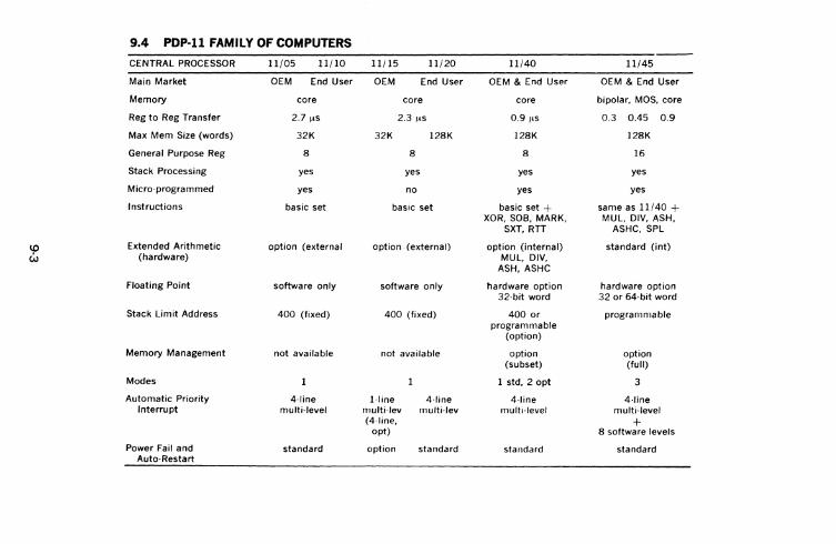
9.4 PDP·ll FAMILY OF COMPUTERS
CENTRAL PROCESSOR 11/05 11/10 11/15 11/20 11/40 11/45
Main Market OEM End User OEM End User OEM & End User OEM & End User
Memory core core core bipolar, MOS. core
Reg to Reg Transfer 2.7 ~s 2.3 ~·s 0.9 ~·s 0.3 0.45 0.9
Max Mem Size (words) 32K 32K 128K 128K 128K
General Purpose Reg 8 8 8 16
Stack Processing yes yes yes yes
Micro-programmed yes no yes yes
Instructions basic set basic set basic set + same as 11/40 + XOR, SOB, MARK, MUL, DIV, ASH,
SXT, RTT ASHC, SPL
10 Extended Arithmetic option (external option (external) option (internal) standard (int) w (hardware) MUL, DIV,
ASH, ASHC
floating Point software only software only hardware option hardware option 32-bit word 32 or 64-bit word
Stack Limit Address 400 (fixed) 400 (fixed) 400 or programmable programmable
(option)
Memory Management not available not available option option (subset) (full)
Modes I 1 1 std, 2 opt 3
Automatic Priority 4-line !·line 4·line 4-line 4-line Interrupt multi-level multi-lev multi-lev multi-level multi· level
(4-line, + opt) 8 software levels
Power Fail and standard option standard standard standard Auto-Restart


APPENDIX A
ISP is a language (or notation) which can be used to define the action of a computer's instruction set. It defines a computer, including console and peripherals, as seen by a programmer. It has two goals: to be precise enough to constitute the complete specification for a computer and to still be highly readable by a human user for purposes of reference, such as this manual. This appendix contains an ISP description of the PDP-11, using a few English language comme11ts
as support,
The following brief introduction to the notation is given using examples from the PDP-11 :-lodel 20 ISP description. The complete PDP-11 descnption follows the introduction.
A processor is completely defined at the programming level by giving its instruction set and its interpreter in terms of basic operations, data types and the system's memory. For clarity the ISP description is usually given in a fixed order:
Declare the system's memory:
Processor state (the information necessary t0 restart the processor if stopped between insttuctions, e.g., general registers, PC, index registers) '
Primary memory state (the memory directly addressable from the processor)
Console state (any external keys, switches, lights, etc., that affect the interpretation process)
Secondary memory (the disks, drums, dectapes, magnetic tapes, etc.)
Transducer state (memory available in any peripheral devtces that is assumed in the instructions of the processor)
Declare the tnstruction format Define the operand address calculation process Declare the data types Declare the operations on the data types Define the instruction interpretation process including tnterrupts, traps, etc. Define the instruction set and the instruction execution process (provides an
ISP expression for each instruction)
Thus, the computer system is described by first declaring memory, data-types and primitive data operations. The instruction interpreter and the instruction-set is then defined in terms of these entities.
The ISP notation is similar to that used in higher level prograrraning languages. Its statements define entities by means of expressions involving other entities in the system. For example, an instruction to increment (add-one) to tnemory would be
Increment := (M[x] ,_ M[x] + l); add one to memor>)J, x
This defines an operation, called "increment", that takes the contents of memory M at an address, x, and replaces it with a value one higher. The := symbol simply assigns a name (on the left) to stand for the expression (on the right). English language comments are given in italics. Table l gives a reference list of notations, which are illustrated below.
ISP expressions are inherently interpreted in parallel, reflecting the underlying parallel nature of hardware operations. This is an important difference between ISP and standard programming languages, which are inherently serial. For example, in
1 The notation derived and used in the book, Computer Structures: Readings and
Examples, McGraw-Hill, 1971 by c. :;ardon Bell and Allen Newell. The book contains ISP) s of 14 computers.
A-1

Z ,. (M[x]- S'+D'; M[y]- M[x]);
both righthand sides of the data transmission operator (~) are evaluated in the current memory state in parallel and then transmission occurs. Thus the old value of M[xJ would go into M[y], Serial ordering of processing is indicated by using the tenn "next", For example,
Z := (M[x] .... S'+D'; next M(y]- M[x});
performs the righthand data transmission after the lefthand one. Thus, the new value of Mlx] would be used for M[yl in this latter case.
:-lemory Declarations
Memory is defined by giving a memory declaration as shown in Table 1. For example,
Mp[0:2k- 1}<15:0::>
declares a memory named, Mp, of 2k words (wher~ k has been given a value), The addresses of the words in memory are 0,1, .•• ,2 -1. Each word has 16 bits and the bits are labeled 15,14, •.• ,0. Some other examples of memory declarations are:
' Boundary -error 2 ) Boundary -error Activity3 N/Negative CC<3', M[o,zl8_1J<7,<1> Ml o, 15][ o,409Sl<7, <1> brop<l: !h 16 } brop<7:o-:-2
boolean meMories; SCYalar bit altel'"rtatives
teM'lai1f digit~ holding value 0~1, or 2 alias~ N and Negative ar>e synonomous bit J of a r>egister> veCYtOl' of 218 8-bit wor>Js Cli'roy o/16 x 4096 8-bit WOI'ds altel'"rtative ways of defining a I'egistei'
using base 16 and b.:1se 2
Renaming and Restructuring of Previously Defined Registers
Registers can be defined in terms of existing registers. In effect, each time the name to the left of the :"' symbol is encountered, the value is computed according to the expression to the right of :=. A process can be evoked to form the value and side-effects are possible when the value is computed.
Examples of simple renaming in part or whole of existing memory
N/Negative := CC<3....,. sp.;lS:O> := Rl6]<15:0>
N is nCV'!e o_f bit J of register CC SP is the same as register R[6]
Examples of register formed by concatenation
LAC<L,O: 11> := LDAC<O: lb AB<0:47> :"" A<0:23>0B<0:23> Mword[0]<15:0> := Mbyte[0]<7:():--Q1byte[l]<7 0>
Examples of values and registers formed by evaluation of a process
ai/address-increment<l: 0> := ( --, byte-op "" 2;
byte-op ~ 1) Run := (Activity "" 0)
Ins true t ion Format
value of ai is 2 if--, byte op, eLse value is 1
Run=l or 0 depending on value of ACYtivity being 0 or not 0
Instruction formats are declared in the same fashion as memory and are not distinguishable as special· non-memory entities. The instructions are carried in a register; thus tt is natural to declare them by giving names to the various parts of the instruction register. Usually only a single declaration is made, the instruction/i, followed by the declarations of the parts of the instruction; the operation code, the address fields, indirect bit, etc.
This declaration would correspond to the usual box diagram:
A-2

Table 1. ISP Character-Set and Expression Forms
A, •.• ,Z,a, .•• ,z,.,-, ...... , ,',",0, ••• ,9
:-i~·x:v·z
n
a := f1expressionl
b(c, •• ,,el :"' g.expression)
name' :"" h(expression\
a- ftexpression) f I expression)
()
{data-type l
boolean ,. expression;
boolean~ Cex.pression-1 else exprP.ssion-2 l;
; next
a/b
XI:"" boolean) ~ expression;
name alphabet. This character set is used for names.
comments, Italics are used for comments.
memory declaration, An n-dimensional memory array of words where a: b ••• v:w are the range of values for the first and last dimensions. The values of the hrst dimension are, for example, a, a+l, ... , b for a s b (or a,a-1, ••• ,b for a ·b), The word length base, z, is normally 2 if not specified. The digits of the word are x,x+l, ••• y.
definition. The ope!'lltor, :=, defines memory, names, process, or operations in terms of existing memory and operations. Each occurrence of "a" causes the in place substitution by f (expression),
The definition b, may have dumny_parameters, c, ••• ,e, which are used in g(expression).
side effects naming convention. In this description we have used ' to indicate that a reference to this name will cause other registers to change.
transmission operator. The contents in register a are replaced by the value of the function.
parentheses. Defines precedence and range of various operations and definitions (roughly equivalent to begin, and end).
operator and data-type modifier
condi tiona! expressiont equivalent to ALGOL ..!f" boolean ~ expression
equivalent to Algol if boolean th.en expression-! else expression-2 - --
sequential delimiter interpretation is to occur
concatenation. Consider the registers to the left and right of D to be one.
statement delimiter. Separates statements.
item delimiter. Separates lists of variables,
division and synonym. Used in two contexts: for division and for defining the name, a, to be an alias (synonym) of the name, b,
unknown or unspecified value
set value. Takes on all values for a digit of the given base, e.g., 1t2 specifies either 102 or 112
instruction value definition. The name X is defined to have the value of the boolean. When the boolean is true, the expression will be evaluated.
A·3

Cormoon Arithmetic, Logical and Relational Operators
~ +add - subtract, also negative x multiply
Logical -,not A and v or
Relational ~1 F not identical = equal
/ divide mod modulo (remainder) ( )2 squared
E9 exclusive-or ;;< equivalence
'f not equal ..., greater than
( )a exponentiation ( ) fa exponentiation ( )b base ( )lb base sqrt ( ) square root abs ( ) absolute value sign-extend ( )
i/ instruction<l5: 0> bop<3: 0> i<l5: 12..., s£<5:0> := i<ll:6"'> df<S:O> : .. i<S:<t>
Operand Address Calculation Process
the inst1'u.ation
0:!: greater than or equal < less than s less than or equal
specifies bin.a1'y ( dyadiaJ operotions specifies sou.1'ae (fi1'st) operun.d e":!Baifie.r; seao7Ul ope1'an.d and destination
In all processors, instructions make use of operands. In most conventional processors, the operand is usually in memory or in the prOcessor, defi.ned as M[z], where z is the effective address. In PDP-11, a destination address, Daddress, is used in this fashion for only two instructions. It is defined in ISP by giving the process that calculates it, This process may involve only accesses to primary memory (possibly indexed) 1 but it may also involve side effects, i.e. 1 the modification of either. of primary memory or processor memory (e.g. 1 by incrementing a register). Note that the effective address is calculated whenever its name is en· countered in evaluating an ISP expression (either in an instruction or in the inter· pretation expression), That is 1 it is evaluated on demand, Consequently, any side effects may be executed more than once.
Operation Detennination Processes
Instead of effective-address, the operands are usually determined directly. For example, the 16-bit destination register is just the register selected by the dr field of an instruction, i.e.,
Rd ,= R[dr] the destination 't'egiste't'
In one other case, the operand is just the next word following an instruction. This next word can be defined,
nw'.:::l5: 0>/next-word :"" (Mw[PC]; PC ... PC+ 2) the nert woN is seleated and PC is moved
Here, the ' shows that a reference to nw will cause side effects, in this case, PC ... PC+ 2. For calculating the source operand, s, the process is:
5'<15,0> ,. (
(sm•O) ~ R[""];
(sm=l) "'Mw[R[sr]]
(am-2) A (sr-7) ~ nw;
value for source opel'and
if mode=O then S' is the Registe1' add't'essed by inst't'uation field s1'
if mode=l the S' is indii"eat via R S'l'
if mode::::::2 and sou.1'ae 't'egistero=FC then the nert wol'd is the ope't'and; this aan be seen by su.bsti tu.ting the ezpression for nw'
A·4

An expreasion h aho needed for the operand, S, which does not cauae the side effecta, and aasuming the effects have taken place, counteracts them. Thus, S
would be:
5<15, II> ,. (
(..,Q) :a R[sr);
<-1) • Mv[R[or)];
<-~) A (or-7) » Mv[PC-2]
no side effe.cts
no side effects
counteract previous side effects
In the ISP ducription a general proceu is given which determines operands for Source-Destination, word-byte, and with-without side-effects. In order to clarify what really happens, the source operand calculation, for words, with side effects, 1a given below.
Sf<S'Il> ,. i<ll: 6>
... 8 , . sf<5: 3>
od ,. sf<3>
••a ,. sf<2: 0>
mr'<U:O> ,. (Mv[PC];
Ro<l5, II> ,. R[or]
S'<15,1l>/Source ,. ((
(.-0) .. Ra;
PC ... PC+2)
( ... 2) A (or/o7) • (Mv[Ro]
Ra ... Ra+2)~
(..-2) 1\ (sr-7) • nw;
(...-4) • (Rs ... Re - 2; next
Mv[Ro]);
(-) A (or/o7) • Mv[nw' + Ro];
<-6) " (or-7) • Mv[nw' + PC];
<-1) • Mv[Ro];
•.-3),!' (or/o7) • (Mv[Mv[Ro)];
Ra ... Rs+2);
(..-3) 1\ (srw7) • M[nv'];
(1111""5) • (Rs ... R8 - 2; next
Mv[Mv[Ro]]);
(01P7) A (or/o7) • Mv[Mv[nw' + Ro)];
(...-7) 1\ (ar-7) • Mw[Mw[nv' +PC])
);
(or-6) A ((-.) v <-5)) "
(SP<4008 ) • (Stack overflow ... 1)
Deta-Txpes
soUI"ce field (6-bitsJ of instr>uction
soUPCe mode control field
defe1"1"ed address control
register specifiaation fo1' soUl'"ce
next wol'd; used as operond
soUPCe roegiste1' specification
value fo1' the sou1'Ce--direct addressing
use the Ngister Rs as O'f.'erand
direct auto-increment ( inC'l'e"Jent
Rs); usually used as POP
diNtct; actually irrmediate operand
diNct; auto-decrement (dee:rement
RaJ; usualLy used as PUSH
direct; indexed via Rs--uses next-word
direct; Nlative to PC; uses next-word value for the source-defiMd addressing
defe1' through Rs
defer through ataak; auto
increment
defer via nezt 1J01'd; absolute add:resaing
defer through staak aftero auto
deC!f'emen.t
defer, indexed via Rs
defer nZ.ative to PC
end ca'l,puZ.ation process;
cheaks if st®k ovel'fiOtJed for several modes
end souree aaZ.aulation
A data-type specifies the encoding of a meaning into an information medium. The .. aning of the data-type (what it designates or refers to) is called ita referent (or value). lbe referent may be anything ranging from highly abstract (the uninterpreted bit) to highly concrete (the payroll account for a specific type of employee).
Every data-type has a carrier, into which all ita component data-types can be Upped. The carrier is used in storing the data-type in memories and is usually a vorct- or multiple thereof. It must be extensive enough to hold all the component data-typea, but may be a larger (having error checking and correcting bits, or
A-5

even unused bits). The .mapping of the component data-types into the carrier is called the format. It is given as a list which associates to each component an expression involving the carrier (e.g., as in the instruction format).
ISP provides a way of naming data -types, which also serves as a basis for abbreviations. Som~ data-types simply have conventional names (e.g., character/ch, qoating point numbers/f); others are named by their value (e.g., integer/i). Datatypes which are iterates of a basic component can be named by the component suffixed by a length-type. The length-type can be array/a, implying a multi-dimensional array of fixed, but unspecified dimensions; a string/ st, implying a single sequence, of variable length (on each occurrence); or a vector/v, implying a one dimensional array of a fixed but unspecified number of components. The length-type need not exist, and then this form of the name is not applicable. Thus, tv is the abbreviation for an integer vector. It is also possible to name a data-type by simply listing its components.
Data-types are often of a given precision and it has becane customary to measure this in terms of the number of components that are used, e.g., Lriple precision integers. In ISP this is indicated by prefixing the precision symbol to the basic data-type name, e.g., di for double precision integer. Note that a double precision integer, while taking two words, is not the same thing as a two integer vector, so that the precision and the length-type, though both implying something about the size of the carrier, do not express the same thing.
A list of common data-types and their abbreviations is given in Table 2.
Operations on Data-types
Operations produce results of specific data-types from operands of specific datartypes. The data-types themselves determine by and large the possible operations that apply to them. No attempt will be made to define the •Jarious .opera-tions here. as they are all familiar. A reasonably comprehensive list is giv_en in Table 1. An operation-modifier, enclosed in braces, { }, can be used to distinguish variant operations. The operation-modifier is usually the name of a data-type, e.g., A+B{f} is a floating point addition. Modifiers can also be a description name applying to the operation, e.g., ax 2 (rotate}.
New operations can be defined by means of forms. For example, the various add operations on differing data·types are specified by writing {data-type} after the operation.
Instruction Interpretation Process
The instruction interpretation expression and the instruction set constitute a single ISP expression that defines the processor's action. In effect, this single expression is evaluated and all the other parts of the 1SP description of a processor are evoked as indirect consequences of this evaluation. Simple interpreter without interrupt facilities show the familiar cycle of fetch-the-instruction and execute-the instruction.
Example: Run= (instruction .... M[PC]; PC .... PC + 1; next This is a simpte
Instruction-execution; next) inter-preter, not the one for the PDP-11
In more complex processors the conditions for trapping and interrupting must also be dexcribed. The effective address calculation may also be carried out in the interpreter, prior to executing the instruction, especially if it is to be calculated only once and will have a fixed value independent of anything that happens while executing instructions. Console activity can also be described in the interpreter, e.g., the effect of a switch that permits stepping through the program under manual· control. or interrogating and -changing memory.
The normal statement for PDP-11 interpretation is just:
..., Interrupt-rq A Run~ (instruction ... Mw[PC]; PC ... PC + 2; next Instruction-execution; next -T-flag • (State-change(l48 ); T-flag ... 0))
A·6
fetah euaute troaae mode

Table 2. Common Data-Types Abbreviations
Primitive ~r boolean by bvte ch character ex complex df double precision floating dw double word d digit
floating fr fraction hw half word
integer mixed number
qw quadruple length word tw triple lengtb word
word
String and Vector bv bit,vector by.st byte.string ch.st character,string
jd j -digit number
Instruction-Set and Instruction Execution Process
The instruction set and the process by which each instruction is executed are usually given together in a single definition; this process is called Instruction-execution in most lSP descriptions. This usually includes the definition of the conditions for execution, i.e., the operation code, value, the name of the instruction, a mnemonic alias, and the process for its execution. Thus, an individual instruc.tion typically has the fonn;
MOV (:= bop= 0001 2 ) = ( ro-S';next
.'7/0Ve 1JOY'c1
move SC'I.i.Y'C'e to intermediate register
N - r<:lS ; Yie?ative'.'
(r<..:::rs:o-. = O'i = (Z ,_ 1 else z .... 0); zeY'e-
D .... r); tt•ansrrn't Y'esult to destination
With this format for the instruction, the entire instruction set is simply a list of all the instructions. On any particular execution, as evoked by the interpretation expression, typically one and only one operation code correlation will be satisfied, hence one and only one instruction will be executed.
In the case of PDP-11, the text carries the definition of the individual instructions, hence they are not redefined in the appendix. Instead, the appendix defines the condiLlon for executing the instructions. For example,
MOV : = (bop = 0001 2 l
is given in the appendix, and the action of !10V is defined (in ISP) in the text.
A·7
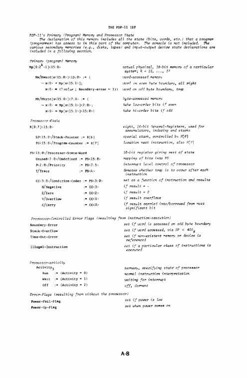
THE PDP-11 ISP
PDP-11 's Pr-imacy (Pl'ogroam) Memoroy and Prtoaessor State The deel.a.Ntion of this memor!~ ineludes all the state (bits, tJol'ds, ete. J that a prog:ram
(prog'!'a!'VT/er) has access to in this parot of the eompute1'. The eonsole is not included. The various secondal'"Y memories (e.g., disks, tapes) and input-output device state dee'taMtions aroe ineluded in a fo llotJing seation.
Primal'"!_J fpl'Ogroam) Memor-y
Mp[0:2k·l]<l5:0> aetual physical, 16-bit memof'}.l o.f a val'ticula:zs system; k ~ 12, •• . , 1?
Mw/Hword[x<l5:0>]<15:0> :"" ( tJOrd-accessed memol'?~
"'"'"~ x<O> = Mp [x<l5: 1>]; worod on et'en hyte bound~, all ttight
x<:O'-> • (? val1.4e ; Boundary-error ... 1)) word on odd byte boundary, tl"aP
Mb/Mbyte[x<l5:0>]<7:0"..> :a ( byte-aceessed memo~
...., x<O> ~ Mp[x<l5:1>)<7:0>; take low-ol'der bits i_f' even
x<O> = Mp[x<l5:b]<l5:8>) take hi-orodel' bits if odd
Processor <State
R(O: 7 ]<15: o-~
sp-:::lS:<t>/StackwPointer :"" R[6]
PC<l5:<t>/ProgramwCounter :• R[7]
PS<l5: 0>/Processor·State-Word
Unused<7: 0>/Undefined : • PS<l5: 8>
P<:-2:0>/Priority
T/Trace
PS<7: 5>
:""' PS<4>
CC<3:0'->/Condition·Codes :• PS<3:0>
N/Negative :• CC<3>
z/zero
V/Overflow
c/ca.rry
:• CC<2>
:• CC<b
:• CC<O>
eight, 16-bit rretteroal-Registeros, used foro accumulato1's, indexing and staeks
speeial staek, eont1'olted b~1 R[6]
loeation next instruetion, also R[?]
16-bit l'egistero giving Nst of state
mapping of bits into PS
interoroupt level aontrool of vrocesso1'
denotes whether> trop is to oeau1' aftero ep.ch instruction
set as a f"uncticm of instr>uction and r>esults
if nsult = -if nsuZ.t = 0
if result overflo!.Js
if roesult ca.rl"ied into/bo1''l'OlJed f1'0m most significant bit
Processor>-Controolled Eroror Flags (l'esulting from instruetion-exeautionJ
Boundary·Ert'or set if tJOrd is accessed on odd b].lte boundary
Stack-Overflow
Time·Out·Error
Illegal- Instruction
ProoeesSOI'-activity Activity3
Run :"" (Activity = 0)
Wait :• (Activity • 1)
Off (Activity • 2)
set if fJJOrd accessed, via SP < 400 8
set if non-existent Memo~ oro device is referoeneed
set if a pa-rticular class of instrouations is executed
teronaroy, speeifyi7'1g state· of p:roaessoro
noZ"!al instruetion inte1'pr>etation
LJaiting foro inte1'l'upt
off, do~t
E1'1'01'-F1.ags (roesulting froom witho_ut the pi'OcessorJ
Power·Fail·Flag
PowerwUp·Flag
set if pO!.Jero is low
set when patJero comes on
A-8

Instruation foPmat field dee!larutions
i.<l5: Ct-/ instruction
bop<3:0> :• i<l5: 12 ~
sf<S: 0"· i<ll:6.
... 8 s£<5: 3
sd ,. s£..:::3
sr8 ,. sf<2: 0~·
df<5: 0> :• i<S:o--
dm8 df<5: 3
dd :• d£<3.
dr8 :• d£<2 :<t•
uop<3: lt:--8 :• i<l5:6:...
df
jsop<7: ()"> i<lS: 9'·
sr; df
brop<l:<t ...... 16 • i<l5:8>
offset<7:0--. :"' s1gn•extend(i<7:0"·)
trop<l;0' ... 16 := i<l5:8'·
unused·trop<l:o-.,.16 :• i<7 (t_.,
eop<6: 0>
er<l:O:>
esf<S: 0>
esm8 esd
fop<7: o-, fr<7:0'>
fsf<5: 0>
15
i<l5: 9>
i<8:6,•
• i<S: 0>
:• es£<5:3>
:= esf<J·:.
:= esf<2: Q_.,
:= 1<15:1t>
1<7:6 ....
:=- i<S:Ct..-
~ df l ~~
jsop j < j I
brop I I I
sd dd
sr I '
df I I
df
binaT'?J ovaode format
SOU'T'C!e _field
sou.roce Mode - 3 bits
souJ"ae rie.fer' bit
sourae roegisteY' - J bits
destination .+'ie ld
destination fflode - 3 bits
destination defer' b1:t
destination register - 3 bits
unal'y op aode (arith., logical, shif'ts)
see binary o.v .+'o:rmat
,-fsr f'o1'mat
see bina1'!J or> [ol'f'lat
bmnah foT"'?at
offset value
trap fo:rmat
extended or>aode f'orrmat
extended Pegister
extended sourae f'ie Zd
mode
defer
1'f!giste1'
floating Clp format
Ngister destination
source
binary operand (2 operands) fonnat
unary operand ( 1 operand), JMP format
JSR format
branch fonnat
value :• sign-extend (offset)
trop I;) unused 171 trap format I I ! I I
eop I esf extended operation format
fop fr fsf floating op fonnat
A-9

ai/address-increment<l:O> = (
...., Byte .. op ~ 2;
Byte-op • 1)
Byte-op :• (MOVB V BICB V BISB V BITB V CLRB V
COMB V INCB V DECB V NEGB V ADCB V
SBCB V TSTB V RORB V ROLB V ASRR V
ASLB V SWAB)
Reserved-instruction := ((i"' ) v (1 = ) v ••• V(i • )) unused instructions
Registers and Data Addressed via Instruction Forrmat Sver::if'ica.tions
nw/next-word<15:0> Mw~PC] used in opel"and deter'mination
nw'/next-word' ,15:0 :• (~tw[PC]; PC- PC+ 2) L>ith side ef"fects
1w/last-word ·15:0 := ~tw[PC- 2] undoes side effects
Rs<15:0-> R[sr]<l5:0>
Rd<l5:()'-. := R[dr]<l5:0>
Operonrf Detemittat1' on fol' Souree and Destination
the source registel"
the destination l"egistel'
Two types of operonds an used: S '~ D '~ Sb' and Db'- for operonds that cause side-effects (i.e.~ othel" l"egistel"s an changed; and S, 0, Sb and Db for opePands that do not cause side ef'feets. Two genel'al procedul"es Wo' and Wo are used to determine these operunds foP side effects and no side effects, l'espectivety
5'<15:0:., := Oprd'<15:0>(Mw, 2,sm,sr)
5<15:0' Oprd<l5:0'>(Mw, 2,sm 1 sv)
Sb'<7:0> Oprd'<7:(t-.(Mb, 2, sm,sr)
Sb<:.7:0> Oprd<7:0>(Mb, 1,sm,sr)
0'<15:0'> Oprd'<lS:D"-~(Mw, 2,dm,dr)
D<15:0"> Oprd<l5:Q:-..(Mw, 2,dm,dr)
Db'<7:0·· Oprd'<7:0">(Mb, 1, dm,dr)
Db--:7:0',..- := Oprd<7:0>(Mb, 1, dm 1 dr)
Genero:z Operocm.d Calculation Pr>ocess (with S1:de Effects)
Oprd'..:wl:lt..>(M,ai,m,rg) :• ((
Rr<ts, !)c. ,. R[rg]
(m=-0) = Rr<wl:Q:-..;
(m•2) 1\ (rg~7) • (M[Rr]; next
Rr ... Rr + ai~ (m•2) 1\ (rg=7) • nw'<wl:O>;
(m=4) • (Rr ... Rr - ai; next
M[Rr]);
(111"6) 11 (rg~7) ,. M[nw' + Rr];
(m•6) 1\ (rg-7) • M[nv' + PC];
(m-1) = M[Rr];
(m=3) 11 (r~7) • (M[Mw[Rr]]; next
Rr ... Rr + 2);
(m-3) 11 (rg"7) ,. M[nw' ];
(m-5) • (Rr o-Rr - ai; next
M[Mw[Rr]]);
A-10
source WOI'd operand side-effects
source wol'd opel'ands no side-effects
source byte
Destination operonds
value for IJOrd Ol' byte operand; dil"ect addressing: wl indicates length; m mode, and rg, ngistel"
secondapY definition for l'egistel'
0, use the Ngister>, R-r, as oper<and
2, dinct auto-incl"ernent (increment
Hl'); usually used in pop stack
2~ direct; next-word is immediate opel'and
4, dil'ect; aftel' auto decl"ement
usuall:y used as PUSH stack
6, dinct; indexed via Hr> uses ne:rtLJOrd
6, diroect; roe lative to PC; uses ne:rtLJOl'd value fol" tJOrd operand defer> addl'eSSin.g
1, defel' thl"ough Rr
3, defel' through MIJ[Rr] (usualty stack),
auto-incl'8ment
3, defer via next-word; absol-ute addressing
5, defer through stack after auto
deci"ement

(m=7) A (rgr7) ~ M[Mw[nw' + Rr]J;
(m'"'n I\ {rg=7) :::o M[Mw[nw' + PC]J;
I;
(rg:6) A ((m=4) v (m=S)) A
(SP < 4008 )) = (Stack-overflow,_ 1)
)
?, dEfer indexed via Rr>
?, defer relative to PC
end C!alau.lation proC!ess
cheC!k i.f stack over>_flows
end operand calculation pr>ocess
General Operand Calculation Pr>oC!ess (t.Jithou.t Side Effects)
Oprd<wl: 0-:>(M,ai,m,rg) := (
Rr<lS; 0> ;= R[rg]
(m=O) = Rr<wl: 0>;
(nP2) I\ (rg;J7) = Mw[Rr - ai};
(mz2) 1\ (rg=7) = lw--..wl: 0'~;
(1TP'4) = M[Rr];
(m:=6) 1\ (rg;J7) = M[lw + Rr];
(mE6) I\ (rg=7) = M(lw +PC];
(m:l) = M[Rr];
(m=3) A (rgf)) =M[Mw[Rr- 211;
(rn=3) I\ (rg=7) = M[lw];
(m=S) = M[Mw[Rr I I; (rn:7) I\ (rg~7) ~ MlMw[lw + Rr]];
(m=7) I\ (rg'f7) = M[Mw[lw + PC]])
Destination addresses for JMP and JSR
Da<l5: 0> ((
(<lnP<O) "' (?; Illegal-instruction .- 1);
(dm=2) A (drr)) = (Rd; Rd ~ Rd + 2);
(dtn=<2) I\ (dr=7) = (PC; PC ,_ PC + 2);
(dm=4} = (Rd - Rd - 2; next Rd);
(dm=6) I\ (d~7) :::o (nw' + Rd);
(dm=6) I\ (dr=7) "' (nw' +,PC);
(dm=l) =~> Mw[Rd];
(dm=3) A (drr)) = (Mw[Rd]; Rd ~ Rd + 2);
(dm=3) I\ (dr=7) = nw';
(dm=5) =t (Rd ,_ Rd - 2; next Mw[Rd]);
(dm=7) I\ (drf7) = Mw[nw + Rd];
(dm=7) I\ (dr=7) = Mw[nw' + PC]); next
undo rr>ev:·ous side-2_f.F'ects
undo tJr>evious s:·de-ef'fects
undo ni'eviou," side-effects
undo prev1:ous side-eff'ect:;
undo pi'ev:'ous side-effects
w:d:::; pr>evious s::de-eff'ects
undo previous side-effects
ur.do p.re!Jiou.s side-ef'.fects
dir>eats:
illegal register> address
auto-incroement
null
auto- dearef'lent
indexed
r>elative
defers:
via register
via auto-inerement
absolute address
auto-decre""!ent
via index
r>elative to PC
(dr==6) A-, ((dm=O) V(dm:=3) v (dm=7)) 1\ (SP < 4008 ) =(check for stack overflow
stack-overflow,_ l))
Data Type Formats
by/byte<7' 0>
w/word<l5: 0>
wi/word. integer<l5: 0>
bybv/byte. boolean-vector<.J: ()_;.
wbv/word. boolean-vee toK15. 0>
d/d.w/double.word<31: Ct>
A-ll

t/d. f/doub1e.word. floating<31: 0>
fs/floating.sign :• £<31>
fe/f1oating.exponent<7:Ct> :• £<30:23>
tm/floating.mantissa<.22:0> • £<22:0>
t/ triple.word<4 7: Ct>
o) quadruple.word<63: 0>
qf/ quadruple.word.f1oating-point<63 0'-->
qfs := q£<63>
qfe :"' q£<62:55>
qfm :• q£<54:0>
I/0 Devices and InteiTupte~ State Infomation
Device[O:N-1]
Device-name[J]<15:0> :"' J
Device-interrupt·1ocation(J]<l5:0> :~ K
dob/device·output-buffer(J ]<15: 0>
d ib/ device-input-buffer (J }<15: 0>
ds/device-status [J]<15: 0>
N I/0 deviaes - asswne devioe J
nwnber to whioh device responses and is addnssed
each device has a value~ K~ whiah it uses as an address to interrupt processor
program aontro'Lled device data
a l"egister !Jith device control state
conrnon derr/device-error-flags[J}<3:0> :• ds[J)<15:12>
dbusy/device-busy[J] :• ds[J]<ll> status dunit/device-unit•selection[J]<2:0> :• ds[J)<l0:8> assignments
ddone[J] : .. ds(J]<7>
denb/device-done-interrupt-enable ;a ds [J ]<6>
derrenb/device-error·interrupt-enable :• ds(J}<S>
dme/device-1'11emory-extension[J]<4: 3> :• ds [J }<4: 3>
dfnc/device-function[J]<2:0> :• ds[J]<2:0>
dintrqfdevice·interrupt-request(J] :"" (
(ddone(J] A denb[J] V ((derr[J) ~ 0) A derrenb[J)))
di 1/ device-interrupt-level [J ]<7: 4> each device is assigned to 1 of 4 levels
Mapping of Devices into M. Eaah deviae 's Teletype
ngiste1"8 an ITtlpped into primary wol'd memory~ e.g.~
M' [1775608 ] :"' tks/ds[TTY-keyboard]
M' [177562 8] :• tkb/dib[TTY·keyboard]
H' [1775648 ] :• tps/ds[TTY·printer]
H' [177566 8 ] :• tpb/dob[TTY·printer]
Inte1"1'upt Requests
br/bus -request -for-interrupt<7: 4>
(dintrq[O] ~ dil[O]) v
(dintrq[1] ~ dil[1]) v •••
(dintrq[J] • dil[J]) v ...
(dintrq[N] ~ dil[N]))
lnterrupt-rq :,. (intrql 2: p)
intrql/ interrupt -request-level<2: 0>
br<:7>. 7;
....., br-<:7> /1. br<:6>. 6;
-. br<7> A -, br<6> A-, br<5> A br<4> ~ 4)
A-12
keyboard status
keyboal'd input data
teleprinter status
telepl"intel" data to print
OR of all device requests
interorupt if a request is "2: prio"rity/P

Insti"uetion IntezopNtation Proeess
Interrupt-rq 1\ Run • (Normal-interpretation);
Normal-interpretation :• (I ... Hw(PC]; PC ... PC+ 2 next
Instruction-execution; next e:r:eeute
T-flag • (State-change(l48 ); T-flag- 0))
Interrupt-rq 1\ _,Off • (
State-change (Device-interrupt -location[J]);
P ... intrql);
off • ( );
_, Interrupt-rq 1\ Wait • ( ) ;
traee
assume device J inte1'1'Upts
State-change(x) :"" ( .~01' stacking state and roestol"e
SP ... SP - 2; next
Mw[SP] ~ PS;
SP ... SP - 2; next
Mw[SP] ~ PC;
PC ... Mw(x];
PS ~ Mw[x+2]
Boundary-Error ~ (State-change(48 ); soundary•error ... 0)
Time-Out-Error .... (State-change(48 ); Time~ut-Error ... 0)
Power-Fail-Flag • (state-change(24 8); PoWer-Fail-Flag- 0;) DI"ogram must tul""! of'.f f!omvuter
Power-Up-Flag • (PC ... 24 8 ; Power-Up-Flag ... 0; Activity ... 0') Stai"t l1!' on pOJJer-up
bastruetion-Set Def'inition
Each instruation is def'ined in ISP in t~e text~ thei"e.fore~ it !Jill not be repeated here.
ISP fo1' Floating Point Pttocessor/FPP Device-interrupt-location [FPP] :• M' [2448 ]
FEO<:l5: 0>
FOCE :• (FEC02)
tDZE :• (FEC04)
FICE :• (FEc-6)
FVE :• (FEC08)
FUE :• (FECOlO)
FUVE :• (FEC012)
FAC[0:5]<63:0>
Fr<63:0>
FPO<:lS:O>
FPSR<lS: 0>
FER :• FPSR<l5>
FIE :• FPSR<l4>
FIUV:• FPSR<ll>
FlU :• FPSR<lll>
FIV :• FPSR<9>
F!C :• FPSR<8>
FD :• FPSR<7>
FL : • PPSR<6>
FT :• FPSR<5>
IMM :• FPSR<4>
A·l3
floating point processor el'1'o1' eode register
floating op eode er't'or
floating dilJide by ae't'O
floating it1tege't' ~Jon:vel"sion e1'1'01'
floating ovel"jlow
fl.oating underfl.""
floating undefined variable
6 floating point aceumulato:rs
tempOMry floating point Ngister
floating point PC
floating point proocessO't' status register
[loa ting el"l''r
in tel'l'upt enable
inte't'rupt on undefined vazoiable
intel'rupt on undeyoflow
interPupt on. ovePflow
inte'l'Z'Upt on integel" conversio,., er:ro:r
floating double p:recision mode
floating long intege:r mode
floating truncate mode
fLoating maintenaMe mode

FN : • FPSR<3>
FZ '• FPSR<:I>
FV :• FPSR<l>
FC ~· FPSR <0>
Inst1'uation [o1'nr.lt
00<3,11> ,. i<15,12>
FOO<J, II> i<ll' II>
A0<1,11> ,. i<7,6>
Gene1'al Definitions
XL '" ((Fl>-0) ~ 1-2"24 ;
(~1) ~ 1-2·56)
XLL '" 2-128
XUL :• 2127 * XL
JL '" ((FL-O) • 215-1;
(FL-1) 0 231 -1)
Addt"ess Calculation
FPS<63:0> :• (
(elm-O) • FAC(dr);
(clmjiO) • (
(Fl>-0) • 0<15,11>01w(PC+2);
(~1) • 0<15,II>OIII[PC+2)C
Mw[PC+4 )OIII[PC+6)))
FPS'<63,11> ,. (
(-0) • FAC(dr);
(clmjiO) ~ (
(Fl>-0) • D'<15,11>0.W'
(FD-1) • D'<lS:O>ChW'taw'lbW'))
FPD<63, II> '" FPS<63, II>
FPD'<63:0>:• FPS'<63:0>
FS<15,11> ,. 0<15,11>
FS'<l5:0> :• D'<lS:O>
FD<15' II> ,. D<15' II>
FD'<lS: 0> :• D'<15: 0>
Fac :• FAC(AC)
a 17 bit result, r, used only for descriptive purposes
floating negative
floating aero
fl.oati"f! overflow
floati"f! ''"'"!!
op code
fl.oati"f! op code
lU!cumul.ato1'
lat"gest [ruction
sm:zllest non-aero numbe1'
ZaPgest numbe1'
l.azogest integer
floating point pPoaessor source
floating point pzoocessor sourcs lUith side effeats
floating point processor destination
floating point processo1' destination Llith side effects
floating source, CPU mode
floating eou.rce tJith side effeats, CPU mode
floating destination, CPU mode
floating destination tJith side effects, CPU mode
destination f1,oating PBgister
2 A prime is used in S (e.g. 1 S') and D (e.g. 1 D') to indicate that when a word is acceseed in this fashioL1 1 side effects may occur. 'That is, registers of R may be changed.
3 !!. all 16 bits of result, r • 0, !!!!.!!. Z is set to 1 else Z is set to 0.
4 The 8 least significant bits are used to form a 16-bit positive or negative number by extending bit 7 into 15:8.
5 a = b means: g boolean a is true !!!..!!.!. ·b is executed.
6 Hw means the memory taken as a work-organized memory.
A-14

APPENDIX B MEMORY MAP
INTERRUPT VECTORS.
000 RESERVED 004 TIME OUT. BUS ERROR 010 RESERVED INSTRUCTION 014 DEBUGGING TRAP VECTOR 020 lOT TRAP VECTOR 024 POWER FAIL TRAP VECTOR 030 EMT TRAP VECTOR 034 "TRAP" TRAP VECTOR 040 SYSTEM SOFTWARE 044 SYSTEM SOFTWARE 050 SYSTEM SOFTWARE 054 SYSTEM SOFTWARE 060 TTY IN·BR4 064 TTY OUT -BR4 070 PCll HIGH SPEED READER-BR4 074 PC11 HIGH SPEED PUNCH 100 KWllL · LINE CLOCK BR6 104 KW11P · PROGRAMMER REAL TIME CLOCK BR6 120 XV PLOTTER 124 DR11B-(BR5 HARDWIRED) 130 AD01 BR5-(BR7 HARDWIRED) 134 AFCll FLYING CAP MULTIPLEXER BR4 140 AAll-A,B,C SCOPE BR4 144 AAll LIGHT PIN BR5 170 USER RESERVED 174 USER RESERVED 200 LP11 LINE PRINTER CTRL-BR4 204 RFll DISK CTRL-BR5 210 RCll DISK CTRL-BR5 214 TCll DEC TAPE CTRL-BR6 220 RKll DISK CTRL-BR5 224 TMll COMPATIBLE MAG TAPE CTRL-BR5 230 CRll!CMll CARD READER CTRL-BR6 234 UDCll (BR4, BR6 HARDWIRED) 240 11145 PIRQ 244 FPU ERROR 254 RPll DISK PACK CTRL-BR5 260 264 270 USER RESERVED 274 USER RESERVED
300 START OF FLOATING VECTORS
8·1

DEVICE ADDRESSES
NOTE: XX MEANS A RESERVED ADDRESS FOR THAT OPTION. OPTION MAY NOT USE IT BUT IT WILL RESPOND TO BUS ADDRESS.
777776 777774 777772 777716 777676 777656 777646 777636 777626 777616 777606 777576 777574 777572 777570 777566 777564 777562 777560 777556 777554 777552 777550 777546
777516 777514 777512 777510
777476 777474 777472 777470 777466 777464 777462 777460
777456 777454 777452 777450 777446 777444 777442 777440
CPU STATUS STACK LIMIT REGISTER 11145 PIRQ REGISTER TO 777700 CPU REGISTERS TO 777600 11145 SEGMENTATION REGISTER TO 777650 MX 11 # 6 TO 777640 MX11 #5 TO 777630 MX11 #4 TO 777620 MX11 #3 TO 777610 MX11 #2 TO 777600 MX11 # 1 11!45SSR2 11/45 SSRl 11/45 SSRO CONSOLE SWITCH REGISTER KL11 TTY OUT DBR KL11 TTY OUT CSR KL11 TTY IN DBR KL11 TTY IN CSR PCll HSP DBR PCll HSP CSR PCll HSR DBR PCll HSR CSR LKS LINE CLOCK KWll-L
LPll DBR LP11 CSR LPll XX LPll XX
RFll DISK RFLA LOOK AHEAD RFll DISK RFMR MAINTENANCE RF11 DISK RFDBR RF 11 DISK RFDAE RF 11 DISK RFDAR RF 11 DISK RFCAR RFll DISK RFWC RF 11 DISK RFDSC
RCll DISK RCDBR RCll MAINTENANCE RCll RCCAR RCll RCWC RCll RCCSR-RCll RCCSR1 RCll RCER RCll RCLA
8-2

777434 DT11 BUS SWITCH # 7 777432 BUS SWITCH # 6 777430 BUS SWITCH # 5 777426 BUS SWITCH # 4 777424 BUS SWITCH # 3 777422 BUS SWITCH # 2 777420 BUS SWITCH # 1
777416 RKDB RKll DISK 777414 RKMR 777412 RKDA 777410 RKBA 777406 RKWC 777404 RKCS 777402 RKER 777400 RKDS
777356 TCXX 777354 TCXX 777352 TCXX
777350 TCDT DEC TAPE (TCll) 777346 TCEIA 777344 TCWC 777342 TCCM 777340 TCST
777336 ASH EAE (KE11-A)#2 777334 LSH 777332 NOR 777330 sc 777326 MUL 777324 MQ 777322 AC 777300 DIV
777316 ASH EAE (KEll-A)# 1 777314 LSH 777312 NOR 777310 sc 777306 MUL 777304 MQ 777302 AC 777300 DIV
777166 CRll XX 777164 CRDBR2 CR 11 CARD READER 777162 CRDBR1 777160 CRCSR
776776 AD01-D XX 776774 A001-D XX 776772 ADDBR AID CONVERTER A001-D 776770 ADCSR
8·3

776766 776764 776762 776760 776756 776754 776752 776750 776740 776736 776734 776732 776730 776726 776724 776222 776720 776716 776714 776712 776710
DAC3 DAC AA 11 DAC2 DACl DACO SCOPE CONTROL - CSR AAll XX AAll XX AAll XX RPBR3 RPll DISK RPBR2 RPBRl MAINTENANCE # 3 MAINTENANCE # 2 MAINTENANCE # 1 RPDA RPCA RPBA RPWC RPCS RPER RPDS
776676 TO 776500 MULTI TIY FIRST STARTS AT 776500
776476 TO 776406 MULTIPLE AAll'S SECOND STARTS@ 776760 776476 TO 776460 5TH AAll 776456 TO 776440 4TH AAll 776436 TO 776420 3RD AA 11 776416 TO 776400 2ND AAll NOTE 1ST AA 11 IS AT 776750
776377 TO 776200 DXll 775600 DSll AUXILIARY LOCATION 775577 TO 775540 DSll MUX3 775537 TO 775500 DSll MUX2 775477 TO 775440 DSll MUXl 775436 TO 775400 DSll MUXO 775377 TO 775200 ON ll 775177 TO 775000 DMll 774777 TO 774400 DPll 774377 TO 774000 DCll
773777 TO 773000 DIODE MEMORY MATRIX
773000 BM792-YA PAPER TAPE BOOTSTRAP 773100 BM792-YB RC,RK,RP,RF AND TCll - BOOTSTRAP 773200 BM792-YC CARD READER BOOTSTRAP 773300 773400 773500 773600 773700 RESERVED FOR MAINTENANCE LOADER
8-4

772776 TO 772700 TYPESET PUNCH 772676 TO 772600 TYPESET READER
772576 AFC-MAINTENANCE 772574 AFC-MUX ADDRESS 772572 AFC-DBR 772570 AFC-CSR 77.2546 KW11P XX 772544 KW11P COUNTER 772542 KW11P COUNT SET BUFFER 772540 KW11P CSR 772536 TM 11 XX 772534 TM 11 XX 772532 TM 11 LRC 772530 TM 11 DBR 772526 TM11 BUS ADDRESS 772524 TM11 BYTE COUNT 772522 TM 11 CONTROL 772520 TM 11 STATUS 772512 OST CSR 772510 OST EADRS1,2 772506 OST ADRS2 772504 OST ADRS1 772502 OST MASK2 772500 OST MASK 1 772416 DR11B/DATA 772414 DR118/STATUS 772412 DR118/BA 772410 DR118/WC 772136 TO 772110 MEMORY PARITY CSR 772136 15 772120 4 772116 3 772114 2 772112 1 772110 0 771776 UDCS ·CONTROL AND STATUS REGISTER 771774 UDSR ·SCAN REGISTER 771772 MCLK ·MAINTENANCE REGISTER 771766 UDC FUNCTIONAL l/0 MODULES 771000 UDC FUNCTIONAL l/0 MODULES 77.0776 TO 770700 KG11 CRC OPTION 770776 KGllA KGNU7 770774 KGDBR7 770772 KGBBC7 770770 KGCSR7 770716 KGNU1 770714 KGBCC1 770712 KGDBR 1 770710 KGCSR1 770706 KGNUO 770704 KGDBRO 770702 KGBCCO
8·5
770700 KG11A KGCSRO 770676 TO 770500 16 LINE FOR DMllBB 770676 DMllBB # 16 770674 770672 770670 770666 DMllBB # 15 770664 770662 770660 770656 DMllBB # 14 770654 770652 770650 770646 DMllBB # 13 770644 770642 770640 770636 DMllBB # 12 770634 770632 770630 770626 DMllBB # 11 770624 770622 770620 770616 DMllBB # 10 770614 770612 770610 770606 DMllBB #9 770604 770602 770600 DMllBB #8 770076 LATENCY TESTER 770074 LATENCY TESTER 770072 LATENCY TESTER 770070 LATENCY TESTER 770056 TO 770000 SPECIAL FACTORY BUS TESTERS 767776 TO 764000 FOR USER and SPECIAL SYSTEMS---DRllA ASSIGNED IN USER AREA-STARTING AT HIGHEST ADDRESS WORKING DOWN 767776 DRllA #0 767774 767772 767770 767766 DRllA # 1 767764 767762 767760 767756 DR 11A # 2 767754 767752 767750
8·6

764000 START NORMAL USER ADDRESSES HERE AND ASSIGN UPWARD. 760004 TO 760000 RESERVED FOR DIAGNOSTIC· SHOULD NOT BE ASSIGNED
8-7


APPENDIX C
PDP-11/ 40 INSTRUCTION TIMING
INSTRUCTION EXECUTION TIME The execution time for an instruction depends on the instruction itself, the modes of addressing used, and the type of memory being referenced. In the most general case, the Instruction Execution Time is the sum of a Source Address Time, a Destination Address Time, and an Execute, Fetch Time.
lnstr Time :: SRC Time + DST Time + EF Time
Some of the instructions require only some of these times, and are so noted. All Timing information is in microseconds, unless otherwise noted. Times are typical; processor timing can vary ± 10%.
I. BASIC INSTRUCTION SET TIMING
Double Operand all instructions,
except MOV: lnstr Time == SRC Time + DST Time + EF Time MOV Instruction: lnstr Time == SRC Time + EF Time
Single Operand all instr, except MFPI, MTPI: lnstr Time == DST Time + EF Time MFPI, MTPI instructions: lnstr Time == EF Time
Branch, Jump, Control, Trap, & Mise all instructions: lnstr Time == EF Time
NOTES: 1. The times specified generally apply to Word instructions. In most
cases Even Byte instructions have the same times, with some Odd Byte instructions taking longer. All exceptions are noted.
2. Timing is given without regard for NRP or BR servicing. Memory types MMll·S, MF11-L, and Mllll are assumed with direct use ot the special processor MSYNA signal and with memory within the CPU mounting assembly. Use of the regular Unibus BUS MSYN signal means 0.08 l'sec must be added for each memory cycle.
3. If the Memory Management (KT11-D) option is installed, instruction execution times increase by 0.15 1£5ec for each memory cycle used.
C·1

SOURCE ADDRESS TIME
Instruction Source Mode SRC Time (A) Memory Cycles
0 0.00 ~sec 0 1 .78 1 2 .84 1
Double 3 1.74 2 Operand 4 .84 1
5 1.74 2 6 1.46 2 7 2.36 3
NOTE (A): For Source Modes 1 thru 7, add 0.34 ~sec for Odd Byte in· structions.
DESTINATION ADDRESS TIME
Instruction Destination Mode DST Time (B) Memory Cycles
Single 0 0.00 ~sec 0 Operand, 1 .78 ( .90) 1 and 2 .84 ( .90) 1 Double 3 1.74 (1.80) 2 Operand 4 .84 ( .90) 1 (except 5 1.74 (1.80) 2 MOV, JMP, JSR) 6 1.46 (1.74) 2
7 2.36 (2.64) 1
NOTE (B): For Destination Modes 1 thru 7, add 0.34 ~sec for Odd Byte instructions. Use higher values in parentheses ( ) for ADD, SUB, CMP, BIT, BIC, or BIS and a Source Mode of 0.
EXECUTE, FETCH TIME
Double Operand
Instruction
use with SRC ( T ime & DST Time)
ADD, CMP, } BIT, BIC, BIS SUB XOR
SRC Mode 0 DST Mode 0
EF Mem Time Cyc
0.99 ~s 1
.99 1
.99 1
SRC Mode 1 to 7 SRC Mode 0 to 7 DST Mode 0 DST Mode 1 to 7
EF Mem EF Mem Time Cyc Time (C) Cyc
1.60 p.S 1 1.76 ~s 2
1.60 1 1.90 2 - - 1.76 2
NOTE (C): For Destination Modes 1 thru 7, add 0.48 ~sec for Odd Byte instructions.
C-2

EFTime DST SRC EFTime (Odd or Memory
Instruction Mode Mode (Word instr) Even Byte) Cycles
0 0 0.90 ~'sec 1.80 ~'sec 0 0 1 to 7 1.46 1.80 0
1 0 to 7 2.42 2.56 2 2 Oto 7 2.42 2.56 2
MOV 3 0 to 7 3.18 3.32 3 4 Oto 7 2.42 2.56 2
(use with 5 Oto 7 3.18 3.32 3 SRC Time)
6 0 2.84 2.98 3 6 1 to 7 3.18 3.32 3 7 0 3.68 3.82 4 7 1 to 7 4.02 4.16 4
Single Operand
Instruction Destination Mode 0 Destination Mode 1 to 7
Mem Mem (use with DST Time) EF Time Cycles EF Time (D) Cycles
CLR, COM, NEG, INC, DEC, ADC, SBC, TST, 0.99!-'S 1 1.77 i<S 2 ROL, ASL, SWAB
ROR,ASR 1.25 (E) 1 2.06 2 SXT .90 1 1.77 2
NOTE (D): For Destination Modes 1 thru 7, add 0.48 ~'sec for Odd Byte instructions.
NOTE (E): For RORB and ASRB, add 0.14 ~<sec for Even or Odd Byte instructions.
Instruction lnstr Time Mem Cycles Note
MFPI MTPI
3.74 i<S 3.68
Branch Instructions
Instruction
BR, BNE, BEQ, BPL, BMI,I BVC, BVS, BCC, BCS, BGE, BL T, BGT, BLE, BH I, BLOS, BH IS, BLO
SOB
2 2
lnstr Time (Branch)
1.76~-'sec
2.36
C-3
These two instructions are im· plemented only if Memory Management is installed.
lnstr Time (No Branch)
1.40 ~<Sec
2.04
Memory Cycles
1
1

Jump Instructions
Instruction Destination Mode lnstr Time Memory Cycles
1 1.80 l'sec 1 2 2.10 1 3 2.30 2
JMP 4 1.90 1 5 2.30 2 6 2.36 2 7 2.92 3
1 2.94 2 2 3.24 2 3 3.44 3
JSR 4 3.04 2 5 3.44 3 6 3.50 3 7 4.06 4
Control, Trap, & Mise: Instructions
Instruction lnstr Time Mem Cyc Notes
RTS 2.421'sec 2 MARK 2.56 2 RTI, RTT 2.92 3
SET N,Z,V,C 1.72 1 CLR N,Z,V,C 2.02 1
HALT 2.42 1 Console loop for a switch setting is 0.44 l'sec.
WAIT 2.24 1 WAIT loop for a BR is 1.12 !'Sec.
RESET SO msec 1
lOT, EMT 5.80 l'sec 5 TRAP, BPT
UTENCY
Interrupts (BR requests) are acknowledged at the end of the current in· struction. For a typical instruction, with an instruction execution time of 4 l'sec, the average time to request acknowledgement would be 2 !'Sec.
Interrupt service ,time, which is the time from BR acknowledgement to the first subroutine instruction, is 5.42 l'sec, max.
NPR (DMA) latency, which is the time from request to bus mastership for the first NPR device, is 3.50 l'sec, max.
C-4

II. EIS, KEll·E, INSTRUCTION TIMING
Source Mode
0 1 2 3 4 5 6 7
Instruction
MUL DIV
ASH (right) ASH (left)
lnstr Time = SRC Time + EF Time
SRC Time
0.28,.sec .78 .98
1.74 .98
1.74 1.74 2.64
EF Time
8.88 ,.sec 11.30
2.58 2.78
Notes
Add 0.30 ,.sec per shift. Add 0.30 ,.sec per shift.
ASHC (no shift) 2.78 ASHC (shift) 3.26 Add 0.30 ,.sec per shift.
LATENCY
Interrupts are acknowledged at the end of the current instruction. Interrupt service time is 5.42 ,.sec, max. NPR latency is 3.50 ,.sec, max.
Ill. FLOATING POINT, KEll·F, INSTRUCTION TIMING
lnstr Time=Basic Time+Shift Time for binary pts+Shift Time for norm
Time per shift to Time per shift lnstr Basic Time line up binary points for normalization
(0 to 23 shifts) (0 to 25 shifts)
FADD 18.78,.sec 0.30 ~'sec 0.341-'sec FSUB 19.08 .30 .34 FMUL 29.00 .34 FDIV 46.72 .34
Basic instruction times shown for FADD and FSUB assume exponents are equal or differ by one.
C·5

LATENCY
If an interrupt request of higher priority than the operating pro~ram occurs during a Floating Point instruction, the current instruction w1ll be aborted unless it is near completion. The maximum time from interr~pt ~equest to acknowledgement during Floattng Point instruction executlo.n IS 20.08 J.'Sec. Interrupt service time is5.42 .usee, max. NPR latency IS
3.50 J.'Sec, max.
C-6
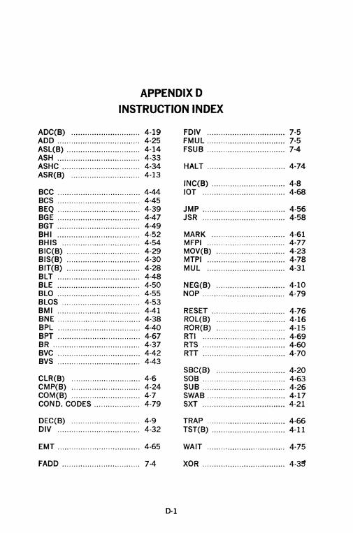
APPENDIXD INSTRUCTION INDEX
ADC(B) .............................. 4-19 FDIV .................................. 7-5 ADD .................................... 4-25 FMUL ................................. 7-5 ASL(B) ................................ 4-14 FSUB .................................. 7-4 ASH .................................... 4-33 ASHC .................................. 4-34 HALT .................................. 4-74 ASR(B) .............................. 4-13
INC(B) ................................ 4-8 BCC .................................... 4-44 lOT .................................... 4-68 BCS .................................... 4-45 BEQ .................................... 4-39 JMP .................................... 4-56 BGE .................................... 4-47 JSR .................................... 4-58 BGT .................................... 4-49 BHI .................................... 4~2 MARK ............................... 4-61 BHIS .................................. 4-54 MFPI .................................. 4-77 BIC(B) ................................ 4-29 MOV{B) .. . .. . .. .. .... . .. .. .... ....... 4-23 BIS(B) ................................ 4-30 MTPI .................................. 4-78 BIT( B) .. . .. .. .. .. .... ... .... .... ...... 4-28 MUL .................................. 4-31 BLT .................................... 4-48 BLE .................................... 4-50 NEG(B) .............................. 4-10 BLO .................................... 4-55 NOP ................................... 4-79 BLOS .................................. 4-53 BMI .................................... 4-41 RESET ................................ 4-76 BNE .................................... 4-38 ROL(B) .............................. 4-16 BPL .................................... 4-40 ROR(B) .............................. 4-15 BPT .................................... 4-67 RTI .................................... 4-69 BR ...................................... 4-37 RTS ................................... 4-60 BVC .................................... 4-42 RTT .................................... 4-70 BVS .................................... 4-43
SBC(B) .............................. 4-20 CLR(B) .............................. 4-6 SOB .................................... 4-63 CMP(B) .............................. 4-24 SUB .................................... 4-26 COM(B) .............................. 4-7 SWAB ................................. 4-17 COND. CODES .................... 4-79 SXT .................................... 4-21
DEC(B) .............................. 4-9 TRAP .................................. 4-66 DIV .................................... 4-32 TST(B) ................................ 4-11
EMT .................................... 4-65 WAIT .................................. 4-75
FADD .................................. 7-4 XOR .................................... 4-3~
D-1

NUMERICAL OP CODE LIST
Op Code Mnemonic Op Code Mnemonic Op Code Mnemonic
00 00 00 HALT 00 60 DD ROR 10 40 00 I 00 00 01 WAIT 00 61 DD ROL EMT 00 00 02 RTI 00 62 DD ASR 10 4.3 77 00 00 03 BPT 00 63 DD ASL 00 00 04 lOT 00 64 NN MARK 10 44 00 00 00 05 RESET 00 65 ss MFPI 1 TRAP j 00 00 06 RTT 00 66 DD MTPI 10 47 77 00 00 07 (unused) 00 67 DD SXT
00 01 DD JMP 00 70 00 l 10 50 DD CLRB 00 02 OR RTS (unused) 10 51 DD COMB
j I 10 52 DD I NCB 00 02 10 00 77 77 J 10 53 DD DECB
I (unused) 01 SS DD MOV 10 54 DD NEGB 00 02 27 02 SS DD CMP 10 55 DD ADCB
03 SS DD BIT 10 56 DD SBCB 00 02 3N SPL 04 SS DD BIC 10 57 DD TSTB 00 02 40 NOP 05 SS DD BIS
06 SS DD ADD 10 60 DD RORB 00 02 41 I 10 61 DD ROLB
cond codes 07 OR ss MUL 10 62 DD ASRB 00 02 77 I 07 lR ss DIV 10 63 DD ASLB
07 2R ss ASH 00 03 DD SWAB 07 3R ss ASHC 10 64 00
00 04 XXX BR 07 4R DD XOR ! (unused) 00 10 XXX BNE 10 64 77
07 50 OR FADD 00 14 XXX BEQ 07 50 IR FSUB 10 65 ss MFPD 00 20 XXX BGE 07 50 2R FMUL 10 66 DD MTPD 00 24 XXX BLT 07 50 3R FDIV 00 30 XXX BGT 10 67 00 I 00 34 XXX BLE 07 50 40 I r i (unused)
I J 00 4R DD JSR j (unused) 10 77 77
07 67 77 11 ss DD MOVB 00 50 DD CLR
00 51 DD COM 07 7R NN SOB 12 ss DD CMPB 00 52 DD INC 13 ss DD BITB
10 00 XXX BPL 14 ss DD BICB 00 53 DD DEC 10 04 XXX BMI 15 ss DD BISB 00 54 DD NEG 10 10 XXX BHI 16 ss DD SUB 00 55 DD ADC 10 14 XXX BLOS 00 56 DD SBC 10 20 XXX BVC 17 00 00 l. 00 57 DD TST 10 24 XXX BVS floating
i j point 10 30 XXX BCC, BHIS 17 77 77 10 34 XXX BCS, BLO
D-2

APPENDIX E SUMMARY OF PDPlliNSTRUCTIONS
GENERAL REGISTER ADDRESSING MODE
Mode Name Symbolic Description
0 register R 1 register deferred (R)
2 auto-increment (R)+
3 auto-incr deferred @(R)+
4 auto-decrement -(R)
5 auto-deer deferred @-(R) 6 index X(R) 7 index deferred @X(R)
PROGRAM COUNTER ADDRESSING
2 3 6 7
immediate absolute relative relative deferred
LEGEND
OpCodes
• = 0 for word/1 for byte SS = source field (6 bits) DO = destination field (6 bits)
#n @#A
A @A
R = gen register (3 bits), 0 to 7 XXX= offset (8 bits), +127 to -128 N = number (3 bits) NN = number (6 bits)
Boolaen 1\ =AND v = inclusive OR
-v- = exclusive OR ,....,=NOT
NOTE:
(R) is operand [ex. R2 = %2] (R) is address (R) is adrs; (R)+(l or 2) (R) is adrs of adrs; (R)+2 (R) - (1 or 2); (R) is adrs (R) - 2; (R) is adrs of adrs (R)+X is adrs (R)+X is adrs of adrs
MODE j Reg= 7
operand n follows instr address A follows instr instr adrs +4+X is adrs instr adrs +4+X is adrs of adrs
Operations
( ) = contents of s = contents of source d = contents of destination r = contents of register ~=becomes X = relative address % = register definition
Condition Codes * = conditionally set or cleared - = not affected 0 =cleared 1 =set
• =Applies to the 11/40, & 11/45 computers • =Applies to the 11/45 computer
E-1

SINGLE OPERAND: OPR dst 15 6 5
OP CODE DO
Mnemonic OpCode Instruction dst Result NZVC
General
GLR(B) •osoDD clear 0 0 1 0 0 COM(B) •o51DD complement (1 's) --cJ * * 0 1 INC(B) •o52DD increment d+1 * * * DEC( B) •o53DD decrement d-1 * * * NEG( B) •o54DD negate (2's compl) -d * ~~ * * TST(B) •o57DD test d * * 0 0
Rotate & Shift
ROR(B) •osoDD rotate right ::: ~:t * * ROL(B) •o61DD rotate left * ~~ * * ASR(B) •o62DD arith shift right d/2 * * ~~: ;':
ASL(B) •o63DD arith shift left 2d * * ;': ~::
SWAB 0003DD swap bytes ::: ~:: t,; 0
Multiple Precision
ADC(B) •o55DD add carry d+C ::: ::~ * * SBC(B) .056DD subtract carry d-C ~:t ::: * *
.&. SXT 0067DD sign extend 0 or -1 * * DOUBLE OPERAND: OPR src,dst OPR scr,R or OPR R,dst
15 12 11 6 5
OP CODE ss : I DO I I I
15 9 8 6 5
OP CODE :R I SS OR DO
Mnemonic OpCode Instruction Operation NZVC
General MOV(B) .1SSDD move d ~s * * 0 CMP(B) .2SSDD compare s-d ~:t * * * ADD 06SSDD add d ~s+d * * * * SUB 16SSDD subtract d ~d-s * ':: * *
Logical
BIT( B) .3SSDD bit test (AND) Sl\d * * 0 -BIC(B) .4SSDD bit clear d ~ t-s)" d * * 0-BIS(B) •sssDD bit set (OR) d ~svd * * o_
.a. Register
MUL 070RSS multiply r ~ r x s * * 0 * DIV 071RSS divide r ~ r/s * * * * ASH 072RSS shift arithmetically * * * * ASHC 073RSS arith shift combined * * * * XOR 074RDD exclusive OR d ~r¥d ~~ * 0
E-2

BRANCH B __ location
15
BASE CODE I
8 7
XXX
If condition is satisfied: Branch to location, New PC ~ Updated PC + (2 x offset)
Op Code = Base Code + XXX adrs of br instr +2
Base Mnemonic Code Instruction Branch Condition
Branches
BR 000400 branch (unconditional) (always) BNE 001000 br if not equal (to 0) -=t-0 Z=O BEQ 001400 br if equal (to 0) =0 Z=1 BPL 100000 branch if plus + N=O BMI 100400 branch if minus N=1 BVC 102000 br if overflow is clear V=O BVS 102400 br if overflow is set V=1 BCC 103000 br if carry is clear C=O BCS 103400 br if carry is set C=1
Signed Conditional Branches
BGE 002000 br if greater or eq (to 0) ;::a N¥-V = 0 BLT 002400 br if less than (0) <0 N.orV = 1 BGT 003000 br if greater than (0) >0 Z v (N.orV) = 0 BLE 003400 br if less or equal (to 0) :;;;a Z v (N.orV) = 1
Unsigned Conditional Branches
BHI 101000 branch if higher > CvZ= 0 BLOS 101400 branch if lower or same :::;;; CvZ= 1 BHIS 103000 branch if higher or same ;;::: C=O BLO 103400 branch if lower < C=1
JUMP & SUBROUTINE:
Op Mnemonic Code
JMP JSR RTS
•MARK •SOB
000100 004ROO 00020R 0064NN 077RNN
Instruction Notes
jump PC~ dst jump to subroutine } return from subroutine use same R mark aid in subr return subtract 1 & br (if =F 0) (R) - 1, then if (R) t= 0:
E-3
PC ~Updated PC -(2 x NN)

TRAP & INTERRUPT:
Op Mnemonic Code
EMT 104000 to 104377
TRAP 104400 to 104777
BPT 000003
JOT 000004
RTI 000002
.&RTT 000006
MISCELLANEOUS:
Op Mnemonic Code
HALT WAIT RESET NOP
e SPL
.& MFPI .& MTPI e MFPD e MTPD
000000 000001 000005 000240 00023N
0065SS 006600 1065SS 106600
Instruction
emulator trap (not for general use)
trap
breakpoint trap
input/output trap
return from interrupt
return from interrupt
Instruction
halt wait for interrupt reset external bus (no operation) set priority level (to N)
Notes
PC at 30, PS at 32
PC at 34, PS at 36
PC at 14, PS at 16
PC at 20, PS at 22
inhibit T bit trap
move from previous instr space move to previous instr space move from previous data space move to previous data space
CONDlTION CODE OPERATORS:
15
OP CODE BASE =000240 : I I
Op Mnemonic Code Instruction
CLC 000241 clear C CLV 000242 clear V CLZ 000244 clear Z CLN 000250 clear N CCC 000257 clear all cc bits
SEC 000261 set C SEV 000262 set V SEZ 000264 set Z SEN 000270 set N sec 000277 set all cc bits
E-4
543210
L 0= CLEAR SELECTED CONO CODE BITS 1 =SET SELECTED COND CODE BITS
N Z V C ___ o __ o_ _o __ o ___ 0 0 0 0
___ 1 __ 1_ _1 __ 1 ___
1 1 1 1

PDPll/40 FLOATING POINT UNIT:
FADD FSUB FMUL FDIV
07500R 07501R 07502R 07503R
DEVICE REGISTER ADDRESSES
Device
KWll-L Line Clock
KW11-P Real Time Clock control & status counter
LA30 DECwriter keyboard printer
LPll Line Printer
LT33 Teletype keyboard printer
PCll Paper Tape reader punch
RC11/RS64 Disk (64K words) look ahead disk address error status
floating add floating subtract floating multiply floating divide
Control & Data
Status Buffer
777 546
772 542 772 540 772 544
777 560 777 562 777 564 777 566
777 514 777 516
777 560 777 562 777 564 777 566
777 550 777 552 777 554 777 556
777 456 777 440 777 442 777 444
command & status 777 446 word count 777 450 current address 777 452 maintenance 777 454
RFll/RSll Disk (256K words) 777 472 control status 777 460 word count 777 462 current mem adrs 777 464 disk address 777466 adrs ext error 777 470 maintenance 777 474 segment address 777 476
E-5
NZVC * * 0 0 * * 0 0 * * 0 0 * * 0 0
Inter-rupt Priority
Vector Level
100 BR6
104 BR6
60 BR4 64 BR4
200 BR4
60 BR4 64 BR4
70 BR4 74 BR4
210 BR5
204 BR5

RK11/RK05 Disk Cartridge drive status error control status word count current address disk address maintenance
TC11/TU56 DECtape control command word count current address
TM11/TU10 Magtape status command byte counter current address read lines
777 400 777 402 777 404 777 406 777 410 777 412 777 414
777 340 777 342 777 344 777 346
772 520 772 522 772 524 772 526 772 532
PROCESSOR REGISTER ADDRESSES
Processor Status Word PS-777 776
777 416 220 BR5
777 350 214 BR6
772 530 224 BR5
15 14 13 12 I I tO 8 7 5 4 3 2 I 0
OO=KERNEL• Ot=SUPERVISORe I I =USER•
& Stack Umit Register- 777 774
• Program Interrupt Request - 777 772
General Registers RO - 777 700 (console use only) R1- 777 701
R2-777 702 R3-777 703
Console Switches & Display Register- 777 570
INTERRUPT VECTORS
000 (reserved) 004 Time Out & other errors 010 illegal & reserved instr 014 BPT 020 lOT 024 Power Fail 030 EMT 034 TRAP
E-6
R4-777 704 R5-777 705 R6-777 706 R7-777 707

Address
--744 --746 --750 --752 - 754 --756 --760 - 762
ABSOLUTE LOADER
Starting Address: __ 500 ~
Memory Size: 4K 017 SK 037
12K 057 16K 077 20K 117 24K 137 28K 157
(or larger)
BOOTSTRAP LOADER
Contents
016 701 000 026 012 702 000 352 005 211 105 711 100 376 116 162
E-7
Address Contents
-- 764 000 002 -766 -400 -- 770 005 267 -- 772 177 756 -- 774 000 765 _ 776 177 560 (KB)
or 177 550 (PR)

NOTES

NOTES

NOTES

NOTES

DIGITAL EQUIPMENT CORPORATION ~DmDDmD WORLDWIDE SALES AND SERVICE
MAIN OFFICE AND PLANT
NORTHEAST REGIONAL OFFICE 275 Wyman Street. Waltham, Massachusetts 02154 Telephone. (617}-19l-0320/0DJ TWX· 710-324-6919
WALTHAM 15 Lunda Street, Waltham, Massachusetts 02154 Telephone: (617)-891-1030 TWX 710-324-6919
CAMBRIDGE/BOSTON 8!:19 Main Street, Cambndge, Massechusetts 02139 Telephone· {617)-'191-6130 TWX: 7\0-32Q-1167
ROCHESTER . 130 Aliens Creek Road. Rochester, New York 14618 relephone: (716)-481-1700 TWX: 7t0-25J.-3078
CONNECTICUT 240 Pomeroy Avenue. Meriden. Connecticut 06450 Telephone: [203)-23Hl441/7466 TWX 710-461-0054
MID-ATLANTIC - SOUTHEAST REGIONAL OFFICE US. Route I, Princeton. New Jersey 08540 Telephone' (609)-452-2940 TWX: 510-685-2338
NEW YORK 95 Ceder Lena. Englewood. New Jersey 07631 Telephone· (201)-871--4984, (212)-594-6955. (212)-736-0447 TWX: 710-991-9721
NEW JERSEY 1259 Route 46, Parstppany, New Jersey 07054 Telephone: (201)-335-:n:x> TWX 710-987-8319
PRINCETON U.S. Route I Prmceton. New Jersey Q85o40 Telephone. (609) 452-2940 TWX- 510-665-2338
LONG /$LAND 1 Huntington Quadrangle Suite 1807 Huntmgton Station. New York 117'16 Telephone: {516)-694-4131. (212)-$5-8095
PHILADELPHIA Station Square Three. Paoli, Penn8ylvanie 1!1301 Telephone: (215)-647-4900/4410 TeleK: 510-668-8385
146 Mo11n Street. Maynard, Massachusetts. US A. 01754 • Telephone: From Merropol•tan Boston 646-8600 • Elsewhere (617)-897-5111 TWX 710-347-0212 Cable DIGITAL MAYN Telex· S4-8457
UNITED STATES MID·ATLANTIC- SOUTHEAST {cont.) WASHINGTON Executtve Butldir>g 6811 Kendworth Ave .. Roverdale. Maryland 20840 Telephone (301)-779-1600/752-8797 TWX. 710-826-9662
DURHAM/CHAPEL HILL 2704 Chapel Hill Boulevard Durham. North Carolina 27707 Telephone (919)-489-3347 TWX- 510-927-0912
ORLANDO Suote 130. 7001 Lake Ellenor Drt.,.e, Orlando. Flonda 32809 Telephone (3>5)-851-4450 TWX 810-850.{)100
ATLANTA 2815 Clearvrew Place, Suotl!! 100, Atlanta, Georgoa 30340 Telephor>e- (404)-451-3734/3735/3736 TWX: 810-757-<1223
KNOXVILLE 6311 Kingston Poke. Suote 21E Knox.,.olle, Teronessee 37919 Telephone. (615)-588--6571 TWX 810-583-0123
CENTRAL REGIONAL OFFICE 1650 Frontage Road, Northbrook. Illinois 6(0)2 Telephone. (312)-498-2500 TWX 910-686-0655
PITTSBURGH 400 Penn Center Boulevard Poltsburgh, Pennsylvania 15235 Telephone (412)-2.0.9404 TWX 710-797-3657
CHICAGO 1850 Frontage Road. Northbrook, Illinois 60062 Telephone: (312}--4198-2500 TWX 910-686-0655
ANN ARBOR 23') Huroll View Boulevard, Ann Arbor. Mochigan <C8103 Telephone: (313)-761-1150 TWX· 810-223-6053
OETR0/1 23777 Greenfield Road, Suite 189 Southfield, M1chig11n <Cil>75 Telephone (313)-559-6565
CENTRAL (cont.) INDIANAPOLIS 21 Onachway Dnve - Suite G lndoanapoliS. lnd1ana 46224 Telephone· (317)-243-8341 TWX 810-341-3436 MINNEAPOLIS Su1te 111. 803') Cedar Avenue South, M1nneapolos, Monnesota 55420 Telephone (612)-854-6562·3--4-5 TWX 910-576-2818 CLEVELAND Park Holl Buildong. 35104 Euclid Avenue Wolloughby, Oh1o 44094 Telephone: (216)-9-46-848<1 TWX 810-427-2608
CENTRAL REGION CATEGORY KANSAS CITY 532 East 42'nd St .. Independence, Missouri 64055 Telephone: (816)-461-3440 TWX 816-461-3100 ST LOUIS Suite 110. 115 Progress Parkway, Maryland Heights. Mossouri 6:J>43 Telephone- {314)-878-4310 TWX_ 910-764-0831 DAYTON 3101 Kettering Boulevard. Dayton, Ohio 45439 Telephone- (513}-29<C-3323 TWX- 810--451H676 MILWAUKEE 8531 W. Capotoi Drove. Milwaukee. Wisconsrn 53222 Telephone (414)-463-9110 TWX: 910-262-1199 DALLAS 8855 North Stemmons Freeway. Dallas. Texas 75247 Telephone: (214)-636--48BO TWX 910-861-4000 HOUSTON 3417 Milam Street. Suole A, Houston, Te~as 77002 Telephone (713)-52<1-2961 TWX: 910-881-1651 NEW ORLEANS 3100 Ridgelake Drive. Suite 108 Meteme, Louisiana 70002 Telephone- 504-837-0257
WEST REGIONAL OFFICE: 310 Soquel Way. Sunnyvale. California 94086 Telephone (-408)-735-9200
WEST (cont.) ANAHEIM 801 E. Bell Road. Anaheim, Calilomoe 92805 Telephone (714)-776-6932/8730 TWX. 910-591-1189 WEST LOS ANGELES 1510 Cotner Avenue, Los Angeles, Celttomoa 90025 Telephone. (213)-479-3791/4318 TWX 910-342-6999 SAN DIEGO 6154 Mtss•on Gorge Road, Suite 110 San Doege. Calolomia 92120 Telephone (71<1)-200-7880. 7970 TWX- 910-335--1230 SAN FRANCISCO 1400 Terra Bella. Mountson Voew. California 94040 Telephone· (415)-964---6200 TWX: 910-373-1266 PALO ALTO 560 San Anton <a Road. Palo Alto. Cal1forn1a 943)8
Telephone {415)-969-6200 TWX. 91G-373-1266 OAKLAND 7850 Edgeweter Drive, Oakland. Csltlornoa 9<1621 Telephone (<115) 635-545317830 TWX: 910-366-7238 ALBUQUERQUE 6303 Indian School !'load, N.E .. Albuquerque, N.M. 87110 Telephone. (505)-296-5411/5428 TWX. 910-989-0614 DENVER 2305 South Colorado Boulevard. Su1te #5 Denver. Colorado 80222 Telephone- (3'J3)· 757-3332/756--1656/758-1659 TWX· 910-931-2650
SEATTLE 1521 I 30th N.E. Bellevue, Washmgton 98005 Telephone- (206)-<154-4058/455-5404 TWX: 910-443--23:16
SALT LAKE CITY -431 South 3rd East. Salt Lake City, Utah 84111 Telephone: (1101)-328--9838 TWX: 910-925-5834
PHOENIX 4358 East Broadway Road. Phoenix, Ar1zona 85040 Telephone. (602)-268-3488 TWX: 910-950-<1691
PORTLAiilD Su1te 168 5319 S.W. Canyon Court, Portland, Oregon 97.,.-Telephone: (503)-297-3761/3765

EUROPEAN HEADQUARTERS Drgltal Equipment Corporation International Europe 81 Route de I'Arre 1211 Geneva 26. Switzerland Telephone 42 79 50 Telex: 22683
FRANCE Equrpment Drgltal S.A R.L.
PARIS 327 Rue de Charenton. 75 Parts 12EME, France Telephone 344-76-07 Telex21339
GRENOBLE 10 rue Auguste Ravrer, F-38 Grenoble. France Telephone (76] 87 5601/02 Telex 32 882 F (Code 212)
GERMAN FEDERAL REPUBLIC Drgrtal Equrpment GmbH
MUNICH 8Muenchen 13, Wallensternplatz2 Telephone 0811-35031 Telex 524-226
COLOGNE 5 Koern 41, Aachener Strasse 311 Telephone 0221-404495 Telex· 888-2269 Telegram Flip Chtp Koeln
FRANKFURT 6078 Neu-lsenburg 2 Am Forsthaus Gravenbruch 5-7 Telephone 06102-5526 Telex. 41-76-82
HANNOVER 3 Hannover, Podbrelskrstrasse 102 Telephone 0511-69-70-95 Telex 922-952
AUSTRIA Drgrtal Equrpment Corporatron Gas m b H.
VIENNA Maroahrlferstrasse 136, tt50Vrenna 15, Austna Telephone 855186
UNITED KINGDOM Drgrtal Equrpment Co, Ltd
U.K HEADQUARTERS Arkwnght Road, Readmg, Berks Telephone 0734-583555 Telex 84327
READING The Evemng Post Burldrng, Tassa Road Readrng. Berks
Fountarn House Butts Centre Readrng. RG1 7QN Telephone.Readrng563555 Telex84328
BIRMINGHAM
~~{;~h~~~m~=t;1~~5d.~~tton ~e~~dye~j ~~rwrcks MANCHESTER 13 Upper Precrnct. Walkden, Manchester M28 5AZ Telephone 061-790-8411 Telex 668666
LONDON Briton House. Uxbridge Road. Ealrng, London WS Telephone 01-579-2334 Telex 22371
EDINBURGH Shtel House, Crargshrll, Lrvrngston. West Lothran. Scotland Telephone 32705 Telex 727113
NETHERLANDS THE HAGUE Dt91tal Equopment NV Sor Wonston Churchrlllaan 370 RrJSWtJk/The Hague. Netherlands Telephone 070-995-160 Telex 32533
BELGIUM
Telex 25297
SWEDEN Drgttal Equrpment AB
INTERNATIONAL CANADA (cont.)
3, Ontarro K1YOX7 TWX 610-562-8907
Port Credit, Ontano TWX 610-492"4306
NORWAY GENERAL INTERNATIONAL SALES
Do9rlal Equrpment Corp A/S
Telex 19079 DEC N
DENMARK Drgrtal Equrpment Aktrebola9
SWITZERLAND
56059
ITALY Dtgttal Equrpment SpA
SPAIN
EnngJe Larreta 12, Madrrd 16 Telex27249
Ud
CANADA Drgotal Equrpment ol Canada, Ltd CANADIAN HEADQUARTERS 150 Rosamond Street. Carleton Place. OntariO Telephone (613)-257-2615 TWX 610-561-1651
Telex 94-8457
AUSTRALIA
NEW ZEALAND
Street. Box 2471
JAPAN
Telex TK-6428
JAPAN (cont.) Roker Tradmg Co., Ltd. (sales only) Kozato-Ka1kan Bldg No. 18-14, Nrshrshrmbasht 1-chome Mrnato-Ku. Tokyo. Japan Telephone·5915246 Telex 781-4208
PUERTO RICO Drgrtal Equrpment Corporatron de Puerto Rrco Amencan Atrlrnes Bldg. 804 Ponce De Leon, Mrramar, Puerto Rrco Telephone 809-723-8068/67 Telex 3135-9056
ARGENTINA BUENOS AIRES Coason SA Yrrrey del Prno 4071 Buenos Arres Telephone 52-3185 Telex 012-2284
BRASIL RIO DE JANEIRO- GB Ambrrex SA Rue Cear<'i, 104,2 o e 3 o and11res Fones 221·4560/44,252-9873 Cable RAIOCARDIO
SAO PAULO- SP
52-7806
Rua Cel. Vrcente, 421. 1 o andar Fones 24-7411,24-7696 Cable
CHILE
INDIA
Telex 011-2594Pienty
MEXICO
PHILIPPINES Stanford Computer Corporatron P 0 Box 1508 416 Dasmarrnas St Mantia Telephone 49-68-96 Telex 742-0352


![Test Taker Instructions STEP+[1] · Appendix: System Requirements Processor (CPU) 1 GHz Pentium processor or faster Memory (RAM) 2 GB or more Disk space Not applicable Internet connection](https://static.fdocuments.in/doc/165x107/5e6780df4420036de363d5ff/test-taker-instructions-step1-appendix-system-requirements-processor-cpu-1.jpg)

