Proceedings of the - Istituto Nazionale di Fisica...
106
LNL-INFN (REP) 203/2004 ISBN 88-7337-007-1 Proceedings of the 2 nd SIRAD Workshop INFN Laboratori Nazionali di Legnaro Legnaro, Padova, Italy April 1-2, 2004 Editor A. Candelori INFN Sezione di Padova
Transcript of Proceedings of the - Istituto Nazionale di Fisica...

LNL-INFN (REP) 203/2004 ISBN 88-7337-007-1
Proceedings of the 2nd SIRAD Workshop
INFN Laboratori Nazionali di Legnaro Legnaro, Padova, Italy
April 1-2, 2004
Editor A. Candelori
INFN Sezione di Padova

LNL-INFN (REP) 203/2004 ISBN 88-7337-007-1
PROCEEDINGS OF THE 2ND SIRAD WORKSHOP
INFN Laboratori Nazionali di Legnaro
Legnaro, Padova, Italy April 1-2, 2004
EDITOR Dr. Andrea Candelori
ORGANIZING COMMITTEE
Prof. Dario Bisello Prof. Giovanni Busatto Dr. Andrea Candelori Prof. Alessandro Paccagnella Prof. Jeff Wyss

PROCEEDINGS OF THE 2ND SIRAD WORKSHOP, LNL-INFN (REP) – 203/2004
II
INTRODUCTION The 2nd SIRAD Workshop was dedicated to the study of radiation effects (bulk damage,
total dose and single events) in silicon detectors, electronic devices and systems for Space and High-Energy Physics applications. The purpose of the Workshop was to continue and increase the stimulating interaction within Universities, Institutes, Industries and Companies operating in the Italian Radiation Effect Community and to be a starting point for new collaborations with Italian and foreign Institutions.
The 2nd SIRAD Workshop was held in the Main Conference Room (Aula Villi) of the INFN National Laboratory of Legnaro, April 1-2, 2004: 52 scientists and researchers from different Italian Universities (Padova, Cassino, Torino, Perugia, Pavia), Research Institutes (INFN Section of Padova, Firenze, Bari, Trieste, Perugia, INFN National Laboratory of Legnaro, ENEA, CNR-IASF, CNR-ISOF, CARSO, ITC-irst), Industries (Alenia Spazio, Aurelia Microelettronica, Galileo Avionica, ST Microelectronics, Tecnomare) and Foreign Institutions (CERN, ESA, Helsinki Institute for Particle Physics) participated to the Workshop.
The Workshop highlighted the importance and the interest in Italy and at an international level of the research activities concerning radiation damage in silicon detectors, electronic devices and systems for High Energy Physics and Space applications. The Workshop was divided in four main sessions: 1) Silicon Detectors; 2) Electronics for Space; 3) Electronics for High Energy Physics and Astrophysics Experiments; 4) Facilities for Radiation Testing.
The presentations of the Workshop are online available: http://sirad.pd.infn.it/sirad/WEB/Index.htm.
Finally it was decided to organize the "Italian Group for Radiation Effect Studies, Testing and Applications (IGRESTA)" open to Universities, Research Institutes, Industries and Companies, which are interested to participate. The purpose of IGRESTA is to develop/maintain an Italian coordination of the groups which perform research and/or have interest for studying/developing electronics and sensors for High Energy Physics and Astrophysics experiments, Space applications and/or technological applications of radiation (for instance nuclear techniques for localization of explosive materials, material sterilization, and so on). The IGRESTA WEB page is online available (http://www.igresta.it) for more information. THE WORKSHOP WAS ORGANIZED WITH THE SUPPORT OF -INFN Laboratori Nazionali di Legnaro; -INFN Sezione di Padova; -Dipartimento di Ingegneria dell'Informazione, Università degli Studi di Padova; -Dipartimento di Fisica, Università degli Studi di Padova; -DIMSAT and DAEIMI, Università degli Studi di Cassino. ACKNOWLEDGEMENTS We thank Dr. Graziano Fortuna, Director of INFN Laboratori Nazionali di Legnaro, and Prof. Gianni Zumerle, Director of INFN Sezione di Padova, who supported the organization of the Workshop; Dr. D. R. Napoli for his suggestions to improve the publication.

PROCEEDINGS OF THE 2ND SIRAD WORKSHOP, LNL-INFN (REP) – 203/2004
III
INDEX
SESSION I: RADIATION HARDENING OF SILICON DETECTORS -"STATUS OF THE DEVELOPMENT OF ULTRA RADIATION-HARD SEMICONDUCTOR DETECTORS FOR VERY HIGH LUMINOSITY COLLIDERS",
M. Bruzzi 3
-"RADIATION DAMAGE MEASUREMENTS FOR THE ALICE PIXEL DETECTORS", M. Cinausero, E. Fioretto, G. Prete, L. Vannucci, F. Antinori, R. Dima, D. Fabris, M. Lunardon, S. Martini, S. Moretto, A. Pepato, F. Scarlassara, G. Segato, F. Soramel, R. Turrisi, G. Viesti, A. Candelori, D. Bisello, A. Kaminski, D. Pantano, P. Riedler, G. Stefanini 7
-"DEVELOPMENT OF CZOCHRALSKI SILICON PARTICLE DETECTORS", J. Härkönen, P. Luukka, E. Tuovinen, E. Tuominen 11
-"DEVELOPMENT OF A FABRICATION TECHNOLOGY FOR PIN DIODES ON THINNED SILICON SUBSTRATE", S. Ronchin, M. Boscardin, G.-F. Dalla Betta, P. Gregori, V. Guarnieri, C. Piemonte, N. Zorzi 14
-"RADIATION HARDNESS OF DIFFERENT SILICON MATERIALS AFTER HIGH-ENERGY ELECTRON IRRADIATION",
S. Dittongo, L. Bosisio, M. Ciacchi, D. Contarato, G. D’Auria, E. Fretwurst, G. Lindström 17
SESSION II: RADIATION EFFECTS IN ELECTRONICS FOR SPACE -"ULTRA-THIN GATE OXIDE RADIATION INDUCED WEAR-OUT AFTER HEAVY ION IRRADIATION: A STATISTICAL MODEL",
S. Cimino, A. Cester, E. Mirando, A. Paccagnalla, G. Ghidini, A. Candelori 23
-"DATA RETENTION OF IRRADIATED FLOATING GATE MEMORIES", G. Cellere, L. Larcher, A. Paccagnella, A. Modelli, A. Candelori 27
-"RADIATION INDUCED DEFECTS IN BIPOLAR POWER TRANSISTORS: INFLUENCE OF RADIATION ENERGY", M. Lavalle, U. Corda, P. G. Fuochi, G. Lulli, E. Gorbia 31
"TOTAL DOSE EFFECTS IN POWER MOSFETS", L. Bandiera, A. Paccagnella, S. Cimino, S. Lora 34
-"EXPERIMENTAL STUDY ON THE RELIABILITY OF LOW BLOCKING VOLTAGE POWER VDMOSFET DURING HEAVY ION EXPOSURE",
F. Velardi, F. Iannuzzo, G. Busatto, J. Wyss, A. Sanseverino, G. Currò, A. Cascio, F. Frisina 37
-"RADIATION SUSCEPTIBILITY TRIALS ON COTS CAMERAS FOR THE INTERNATIONAL SPACE STATION", M. Zampato, R. Finotello, R. Ferrario, A. Viareggio, S. Losito 39
-"HEAVY ION TEST ON E2V CCD87 FOR THE AMS-02 EXPERIMENT ON THE INTERNATIONAL SPACE STATION",
M. Albi, A. Bucconi, F. Turchet 43
-"LASER SYSTEM FOR SINGLE EVENT EFFECT TESTING AND RADIATION SENSITIVITY MAPPING OF INTEGRATED CIRCUITS",
M. Petasecca, B. Alpat, R. Battiston, M. Bizzarri, S. Blasko, M. T. Brunetti, D. Caraffini, L. Di Masso, L. Farnesini, E. M. Fiori, M. Menichelli, A. Papi, V. Postolache, G. Scolieri, A. Secchi 47
-"CAN BUS PHYSICAL LAYER RADIATION TEST", S. Chicca, F. Bigongiari, W. Errico, F. Bertuccelli , M. Lippi ,G. Manoni, M. Ceschia 50
-"SINGLE EVENT EFFECTS IN SRAM-BASED FPGAS", M. Ceschia, M. Violante, M. Sonza Reorda, A. Paccagnella, P. Bernardi, M. Rebaudengo, D. Bortolato, M. Bellato, P. Zambolin 53

PROCEEDINGS OF THE 2ND SIRAD WORKSHOP, LNL-INFN (REP) – 203/2004
IV
SESSION III: RADIATION-HARD TECHNOLOGIES FOR ELECTRONICS IN HIGH ENERGY PHYSICS AND ASTROPHYSICS EXPERIMENTS -"BULK DAMAGE IN PROTON IRRADIATED JFET AND JFET-BASED CHARGE SENSITIVE AMPLIFIERS ON HIGH RESISTIVITY SILICON",
L. Ratti, G.-F. Dalla Betta, M. Manghisoni, V. Re, V. Speziali, G. Traversi, A. Candelori 59
-"SINGLE EVENT UPSET MEASUREMENTS ON THE SVX4 CHIP", N. Bacchetta, D. Pantano, Z. Wang 63
-"HEAVY ION IRRADIATION OF THE XAA1.2 ASIC CHIP FOR SPACE APPLICATIONS", E. Del Monte, L. Pacciani, G. Porrovecchio, P. Soffitta, E. Costa, G. Di Persio, M. Feroci, M. Mastropietro, E. Morelli, M. Rapisarda, A. Rubini, D. Bisello, A. Candelori, A. Kaminski, J. Wyss 67
-"RADIATION TESTING OF THE GLAST LAT TRACKER ASICS", R. Rando, A. Bangert, D. Bisello, A. Candelori, P. Giubilato, M. Hirayama, R. Johnson, H. F.-W. Sadrozinski, M. Sugizaki, J. Wyss, M. Ziegler 71
-"RADIATION HARDNESS QUALIFICATION OF THE APV25 CHIP PRODUCTION FOR THE CMS EXPERIMENT", A. Candelori, R. Bainbridge, P. Barrillon, D. Bisello, M. J. French, G. Hall, A. Kaminski, V. Khomenkov, E. Noah, M. Raymond, L. Stefanutti, M. Tessaro 75
SESSION IV: FACILITIES FOR RADIATION TESTING OF DETECTORS AND ELECTRONIC DEVICES -"FACILITIES FOR RADIATION HARDNESS QUALIFICATIONS AT ENEA-CASACCIA", S. Baccaro, A. Cecilia 81
-"THE ELECTRON ACCELERATOR OF THE ISOF-CNR INSTITUTE AND ITS USE FOR INDUSTRIAL APPLICATIONS AND APPLIED RESEARCH",
P. Fuochi, U. Corda, M. Lavalle 85
-"THE PADOVA LABORATORY FOR INTERDISCIPLINARY APPLICATION OF NEUTRONS", G. Viesti, M. Cinausero, M. Lunardon, G. Nebbia, S. Pesente 88
-"THE SIRAD IRRADIATION FACILITY FOR BULK DAMAGE AND SINGLE EVENT EFFECT STUDIES", A. Candelori, D. Bisello, P. Giubilato, A. Kaminski, D. Pantano, R. Rando, M. Tessaro, J. Wyss 91
-"THE ION ELECTRON EMISSION MICROSCOPE FOR SINGLE EVENT EFFECT STUDIES AT SIRAD", D. Bisello, P. Giubilato, M. Nigro, R. Rando, J. Wyss, A. Candelori 96

PROCEEDINGS OF THE 2ND SIRAD WORKSHOP, LNL-INFN (REP) – 203/2004
SESSION I
RADIATION HARDENING OF SILICON DETECTORS

PROCEEDINGS OF THE 2ND SIRAD WORKSHOP, LNL-INFN (REP) – 203/2004

PROCEEDINGS OF THE 2ND SIRAD WORKSHOP, LNL-INFN (REP) – 203/2004
3
Status of the development of ultra radiation-hard semiconductor detectors for very high luminosity colliders
M. Bruzzi on behalf of the RD50 Collaboration
INFN Sezione di Firenze and Dipartimento di Energetica, Università di Firenze, Via S. Marta 3, Firenze, I-50139, Italy
I. INTRODUCTION
The luminosity upgrade to 1035 cm-2×s-1, recently discussed to extend the High Energy Physics research at the Large Hadron Collider (LHC) [1], will require the development of ultra radiation hard semiconductor detectors, able to withstand fast hadron fluences up to 1016 cm-2. The CERN RD50 Collaboration [2], "Development of Radiation Hard Semiconductor Devices for Very High Luminosity Colliders", started in 2002 with the aim to develop a new reliable detector technology available for the LHC upgrade or a future high luminosity hadron collider. Two main research lines have been identified: 1) Material Engineering, with the aim to produce the most intrinsically radiation hard semiconductor material in terms of degradation of the electrical properties after irradiation; 2) Device Engineering, to identify the best geometry (size and position) of the segmented electrodes in order to optimize the radiation resistance of the detector. The activity and the most recent advances of each research line are presented and discussed in this paper.
II. MATERIAL ENGINEERING
This research line is divided into three projects: Defect/Material Characterization (DMC), Defect Engineering (DE) and development of New Materials (NM). The DMC project relies on the detailed study of the microscopic aspects of radiation damage in the semiconductor bulk. Defect Engineering is focussed on the beneficial effect on radiation hardness due to the deliberate addition of selected impurities in the material. The NM project aim is to investigate novel radiation hard semiconductor materials. In this section a review on the most important advances of these projects is presented.
II.A. Defect/Material Characterization
Particles impinging on the semiconductor bulk produce a cascade of primary defects (vacancies (V) and interstitials (I)). They migrate in the lattice and interact with each other or with the existing impurities, creating stable localized defect complexes (point defects) or extended damaged regions (clusters). The ratio of the clusters over point defects depends on the particle type and energy: only point defects are generated by 60Co γ-ray irradiation; both types of defects are created with hadron irradiation; while clusters are dominating the microscopic disorder after fast neutron irradiation [3]. Electrically active defects are responsible of the change in the main macroscopic properties of the particle
detectors: the effective doping concentration of the space charge region (Neff), the full depletion voltage (Vdep), the reverse current at full depletion (Ileak) and the charge collection efficiency (CCE). Thus, a first fundamental step for the definition of the optimal radiation hardening procedure is represented by the exhaustive identification of native and radiation-induced defects, and of their influence on the carrier transport properties in the device. The main tools available for studying defects are Deep Level Transient Spectroscopy (DLTS), Thermally Stimulated Current (TSC) and Photo Induced Transient Spectroscopy (PITS). These techniques are used to determine the activation energy and capture cross sections of the electrically active levels in the forbidden gap and to evaluate the concentration of the related defects in the semiconductor bulk. For the trap identification, the results are compared with the defect signature from a database of parameters of earlier identified defects.
Native or process-induced defects are quite important, as they can directly influence the Neff value before irradiation: particularly, this is the case of thermal donors (TD) in Czochralski (Cz) silicon (Si). The RD50 Collaboration investigated in detail the thermal processes to enhance and/or to suppress TD generation, in view to control the Neff of Cz Si-based diodes before irradiation. A donor killing process can be applied in order to partially deactivate the thermal donors in standard Cz Si and ensure a sufficiently high resistivity material.
Recently, important advancements in understanding the radiation damage in the case of point defects have been performed within the RD50 Collaboration. Point defects are of crucial importance for the radiation hardness of silicon after irradiation with 60Co γ-rays. Three levels have been correlated with the changes of Neff, Vdep and Ileak: two midgap acceptor levels (I and Γ ) and a bistable donor (BD). I and Γ are generated in higher concentrations in standard Float Zone (FZ) silicon than in oxygen enriched Si, while the BD is mainly found in oxygen enriched and epitaxial silicon [4],[5]. The Γ defect, an acceptor level at Ev+0.68 eV, is characterized by linear dose dependence, and it can explain about 10% of the damage. The I defect, of amphoteric nature, having both an acceptor state at Ec-0.54 eV and a donor state at Ev+0.23 eV, has a quadratic dose dependence and it is proven to be the main cause for the space charge sign inversion in standard FZ diodes. The I defect accounts for more than 85% of the damage caused by γ-ray irradiation.
II.B. Defect Engineering of Silicon
Since 1995 the RD48 CERN Collaboration [6] has adopted the strategy to add selected impurities in the

PROCEEDINGS OF THE 2ND SIRAD WORKSHOP, LNL-INFN (REP) – 203/2004
4
silicon bulk in order to beneficially influence the microscopic damage induced by radiation. The key idea in the RD48 proposal was in particular to investigate the influence of oxygen on the silicon radiation hardness. The concentration of interstitial oxygen in Si ([Oi]) is strongly dependent on the growth technique. In high purity Float Zone silicon [Oi]≈1015 cm-3, while in Czochralski silicon [Oi] can reach values as high as 1018 cm-3. The first attempt in the High Energy Physics Community to enrich silicon wafers with oxygen for radiation hardening purposes was made in 1992 at the Brookhaven National Laboratory [7]. As at that time Czochralski silicon was not available with the high resistivity required for a proper application in tracking detectors, an opportune technique was developed to produce Diffusion Oxygenated Float Zone (DOFZ) silicon. By this method silicon was doped with oxygen by high temperature (1200°C) oxidation during 20 to 220 hours, to obtain the Oi concentration of the order of 2×1017 cm-3.
High resistivity Cz Si suitable for detector applications became recently available after proper developments in the crystal growth techniques (see e.g. [8]). Two different Cz materials are under investigation in the framework of the RD50 Collaboration: Magnetic Czochralski (MCz) from Okmetic Ltd (Finland) and standard Cz (SCz) material from Sumitomo-Sitix (Japan). The first material has a resistivity of ≈900 Ω×cm and an oxygen concentration of 3.5×1017 cm-3; the second material has a resistivity of ≈1200 Ω×cm and an oxygen concentration of 8×1017 cm-3.
A different approach for increasing the radiation tolerance of silicon detectors is the use of thin epitaxial silicon layers. Single crystal epitaxial layers of different resistivity and thickness can be grown on different substrates (Cz, FZ). Low resistivity (50 Ω×cm) 50 µm thick epitaxial layers were grown by ITME (Poland) on low resistivity (0.015 Ω×cm) Cz substrates [9].
II.C. New Materials
SiC and GaN, which have physical properties in between those of Si and diamond, can be attractive materials for particle detection. Due to the low leakage current, almost insensitive to radiation, (≈10-10A/cm2), they are potentially radiation-hard.
Preliminary results with α-particles from a 241Am source evidence a 60% CCE for semi-insulating SiC, which is reduced to ≈50% after irradiation by 300 MeV pions up to 1013 cm-2 [10]. A 100% CCE was measured with β-particles from a 90Sr source on 4H-SiC Schottky diodes manufactured with n-type epitaxial wafers (IKZ, Berlin): the measured signal, stable and reproducible, is ≈2200 electrons in the thickest epitaxial layer (≈40 µm) [11].
In preliminary tests with α-particles from a 241Am source on semi-insulating GaN Schottky detectors the CCE reduced from 92% to 77% after irradiation by nuclear reactor neutrons up to 5×1014 cm-² [12]. More studies are still necessary to definitely assess the radiation hardness of these materials as compared to Si.
III. DEVICE ENGINEERING
This research line is divided into three projects: Pad Detector Characterization (PDC), New Structures (NS) and Full Detector Systems (FDS). The PDC project deals with radiation damage studies performed with the simplified geometry of a single pad detector (SPD), i.e. a single-pad p+-n-n+ structure surrounded by a set of guard-rings. The FDS project is focused on radiation damage studies on prototype microstrip and pixel detector modules with LHC-like read-out electronics, while the NS main research activity is to develop novel detector geometries to increase the device radiation hardness. In this section a review on the most important recent results of these three projects is presented.
III.A. Pad Detector Characterization
The use of SPD provides the cost-effective development of radiation tests mainly concentrated on the study of parameters (Neff, Vdep, Ileak, CCE) as a function of the particle fluence. The radiation hardness of SPD made with defect engineered Si (DOFZ, Cz, MCz, and epitaxial) has been investigated by several irradiation campaigns at different facilities, with different particles and energies. These devices exhibit interesting radiation hardness properties [9],[13],[14]. In particular, for Cz Si there is no type inversion after irradiation with 190 MeV pions (PSI) or 24 GeV/c protons (CERN) up to 1015 particles/cm2. The change of Vdep as function of fluence is considerably smaller than that of standard FZ or DOFZ silicon devices. The epitaxial diodes show superior radiation tolerance compared to those fabricated with all the other silicon materials. Fig.1 shows a comparison between epitaxial diodes and diodes fabricated with standard FZ (STFZ) and DOFZ materials. In the full range of the measured fluences rescaled to 1 MeV equivalent neutrons up to 8×1014 cm-2, the epitaxial diodes do not exhibit the space charge sign inversion and show a reduced variation of the full depletion voltage [9].
Figure 1. Comparison of the depletion voltage (Vdep) as a function of the 24 GeV/c proton fluence rescaled to 1 MeV equivalent neutrons (Φeq) for diodes manufactured on different silicon substrates [9].

PROCEEDINGS OF THE 2ND SIRAD WORKSHOP, LNL-INFN (REP) – 203/2004
5
III.B. New Structures
In standard detector geometry, electrodes are placed on opposite sides of the semiconductor, as in parallel plate capacitor geometry. The charge generated by ionizing radiation drifts in the direction perpendicular to the plane of the semiconductor wafer to the oppositely biased electrodes. The charge generated by the impinging radiation is proportional to the sensitive thickness of the detector, therefore to the detector thickness when the device is fully depleted. When the detector suffers high radiation damage, the full depletion cannot be achieved anymore and the charge trapping further reduces the amount of the collected charge drifting for longer distances.
A novel type of device, called 3D detector, was introduced [15] to reduce the electrode distance, therefore increasing the amount of charge collected after heavy irradiation, while keeping the same detector thickness. In 3D devices, the generated charge drifts in the plane of the wafer and the electrode separation is independent of the material thickness. Thus, the 3D geometry may be designed to both maximize signal response to incident radiation and minimize sensitivity to defects arising from radiation damage.
Three different routes to fabricate the 3D geometries have been developed. Depending on particular material system and requirements, one or other of these methods is to be preferred. The electrodes may be produced using plasma etching (micro-machining), femtosecond laser drilling technique, or photo-electrochemical (PEC) etching.
The plasma etching technique is the most compatible with micro-fabrication processes. However, for 3D detector manufacture it is suitable only for silicon and is currently limited to an aspect (depth-to-width) ratio for the holes of about 20:1. PEC will in principle produce holes of arbitrary aspect ratio, but the geometries usable are more limited due to the nature of the process. The laser drilling technique is the most cumbersome, as each electrode is made in sequence. In silicon, plasma etching and PEC produce electrodes in parallel, so both those methods are best suited for volume production of 3D detectors. Plasma etching and laser machining are independent of crystal orientation. PEC is suitable only for specific crystal orientations, which are easily commercially available. The electrodes are then formed in these vias and connected to the read out electronics with deposited metal lines and contacts. Besides the 3D detectors, now developed within RD50 by ITC-irst (Trento), CNM (Barcelona) and Glasgow University, other new geometries are under investigation, namely thin detectors [16] and semi-3D devices [17]. The status of these activities can be found in [18].
III.C. Full Detector Systems
The FDS research line of RD50 aims to test the properties of segmented detectors after heavy irradiation in order to allow the choice of the optimal geometry (diode structure, detector thickness, cell size, and so on) for the targeted radiation fluence and to validate the use of non-standard silicon substrates for the production of
large area segmented devices. The crucial parameter which defines the ability of the detector to provide the tracking information is the signal to noise ratio. The noise is dependent on the particular setup used to read-out the detectors, thus it is important that the detector charge collection efficiency as a function of the reverse bias voltage (i.e., CCE(V)) is evaluated with a LHC-like read-out electronics at the speed of 40 MHz.
CCE(V) of irradiated silicon detectors depends on trap density and on collection time (tc), therefore on the drift velocity of the charge carriers. The amount of the trapped charge is inversely proportional to tc. The charge carrier velocity v depends on the local electric field E(x), i.e. v=µe,h×E(x) where µ is the mobility for electrons (e) and holes (h), until the saturation velocity is achieved. As a consequence, a lower trapping is expected for carriers moving in high electric field (smaller tc).
Silicon detectors are usually manufactured by implanting high doped p-type strips on high resistivity n-type substrates. An ohmic contact (high doped n-type) is implanted on the backplane (p-in-n diode). After space charge sign inversion the junction and consequently the high electric field migrate on the backplane contact and a better charge collection is obtained by segmenting the n-type implant (n-in-n detectors) [19],[20]. The n-side read out can be implemented on n-type or p-type substrates. The use of p-type substrates has the advantages of avoiding substrate type inversion and providing the cheapest processing cost, due to the possibility of one side processing, compared to the double side processing required by n-type silicon substrates.
In a previous study [21], a substantial improvement of the charge collection after irradiation at low bias voltages was observed for standard p-type substrates read-out at the n-side (n-in-p detectors) when compared to p-type substrates read-out at the p-side (p-in-n detectors) [21].
A possible further improvement of the radiation hardness could be obtained with oxygen enriched p-type substrates. The Liverpool University and CNM (Barcelona, Spain) investigated in the framework of the RD50 Collaboration, the charge collection properties of n-in-p microstrip detectors manufacture on oxygenated substrates, comparing their performances with devices produced on p-in-n standard and oxygenated silicon [22]. Standard (oxygenated) detectors were irradiated with 24 GeV/c protons at CERN up to 3×10¹⁵ protons/cm2 (7.5×10¹⁵ protons/cm2). The main result was that even after the highest irradiation fluence, the charge collection of the n-in-p detectors manufactured on oxygenated silicon is higher than 6500 electrons at the maximum applied bias (900 V) [22]. This corresponds to a signal to noise ratio of ≈7.5, which could still be sufficient for efficient tracking. Further studies are required to investigate whether the oxygenation of p-type substrates brings any advantage, but such detectors appear to be suitable for being used as particle detectors also after experiencing extremely high level of fast hadron fluences. ____________________ [1] "Physics potential and experimental challenges of the LHC
luminosity upgrade", CERN-TH/2002-078.
PROCEEDINGS OF THE 2ND SIRAD WORKSHOP, LNL-INFN (REP) – 203/2004
6
[2] "Development of radiation hard semiconductor devices for very high luminosity colliders", LHCC 2002-003, 15 February 2002, CERN, Geneve.
[3] M. Huhtinen, Nucl. Instr. Meth., A491 (2002) 194. [4] I. Pintilie et al., Appl. Phys. Lett., 82 (2003) 2169. [5] I. Pintilie et al., Nucl. Instr. Meth., A514 (2003) 18. [6] RD48. On line available: http://rd48.web.cern.ch/rd48/. [7] Z. Li et al., IEEE Trans. Nucl. Sci., 42 (1995) 219. [8] V. Savolainen et al., J. Crystal. Growth, 2 (2002) 243. [9] G. Kramberger et al., Nucl. Instr. Meth., A515 (2003) 665. [10] W. Cunningham et al., Nucl. Instr. Meth., A509 (2003) 127. [11] F. Nava et al., IEEE Trans. Nucl. Sci., 51 (2004) 238. [12] J.Vaitkus et al., Nucl. Instr. Meth., A514 (2003) 141. [13] J. Härkönen et al., Nucl. Instr. Meth., A518 (2004) 346. [14] G. Lindström et al., "Recent damage results from the HH-CiS
collaboration", 1st RD50 Workshop on Radiation Hard Semiconductor Devices for Very High Luminosity Colliders, CERN, 2-4 October 2002. On line available: http://www.cern.ch/rd50.
[15] S. I. Parker et al., Nucl. Instr. Meth., A395 (1997) 328. [16] Z. Li, "Activities of the US chapter of CERN RD50 on the
development of semi-3D Si detectors", 2nd RD50 Workshop on Radiation Hard Semiconductor Devices for Very High Luminosity Colliders, CERN, 18-20 May 2003. On line available: http://www.cern.ch/rd50.
[17] S. Ronchin et al., "Fabrication of PIN diodes on thinned high resistivity silicon", 6th International Conference on Large Scale Applications and Radiation Hardness of Semiconductor Detectors, Firenze, Italy, 29 September-1 October 2003.
[18] On line available: http://www.cern.ch/rd50/. [19] G. Casse et al., Nucl. Instr. Meth., A511 (2003) 112. [20] G. Casse et al., IEEE Trans. Nucl. Sci., 47 (2000) 527. [21] G. Casse, "First results with oxygenated n-in-p detectors after
irradiation", 2nd RD50 Workshop on Radiation Hard Semiconductor Devices for Very High Luminosity Colliders, CERN, 18-20 May 2003. On line available: http://www.cern.ch/rd50.
[22] G. Casse et al., "Performances of miniature microstrip detectors made on oxygen enriched p-type substrates after very high proton irradiation", presented at the 10th Vienna Conference on Instrumentations, Vienna, Austria, 16-21 Febrary 2004.
PROCEEDINGS OF THE 2ND SIRAD WORKSHOP, LNL-INFN (REP) – 203/2004
7
Radiation damage measurements for the ALICE pixel detectors
M. Cinausero1, E. Fioretto1, G. Prete1, L. Vannucci1, F. Antinori2, R. Dima2, D. Fabris2, M. Lunardon2, S. Martini2, S. Moretto2, A. Pepato2, F. Scarlassara2, G. Segato2, F. Soramel2, R. Turrisi2, G. Viesti2, A. Candelori2, D. Bisello2,
A. Kaminski2, D. Pantano2, P. Riedler3, G. Stefanini3
1INFN Laboratori Nazionali di Legnaro, Viale dell’Università 2, Legnaro (Padova), I-35020, Italy
2 INFN Sezione di Padova and Dipartimento di Fisica, Università di Padova, Via Marzolo 8, Padova, I-35131, Italy
3CERN, Geneva, Switzerland
I. INTRODUCTION
ALICE is an experiment presently under construction at the CERN Large Hadron Collider (LHC). It is primarily designed to investigate the behaviour of strongly interacting matter under the extreme conditions of heating and compression that will be reached in ultra-relativistic nucleus–nucleus collisions at the energy of the LHC. The ALICE experimental apparatus is described in [1].
The inner region, with a radius of about 0.45 m, will be instrumented with the Inner Tracking System (ITS) [2],[3] providing high precision, high granularity tracking close to the primary interaction vertex for the detection of weak decays of strange, charm and beauty particles. The ITS will allow full tracking in the pseudo-rapidity range |η|<1 and a measurement of the charged multiplicity out to |η|<2. It will consist of six concentric layers of silicon detectors: two layers of Silicon Pixel Detectors (SPD), two layers of Silicon Drift Detectors (SDD) and two layers of Silicon Strip Detectors (SSD).
Physics performance constraints have determined the choice of carbon fibre for the support structure, aluminium-based technology for the flex circuitry and low thickness for the silicon sensors and integrated circuits. A description of the status of the ITS system is given in [4].
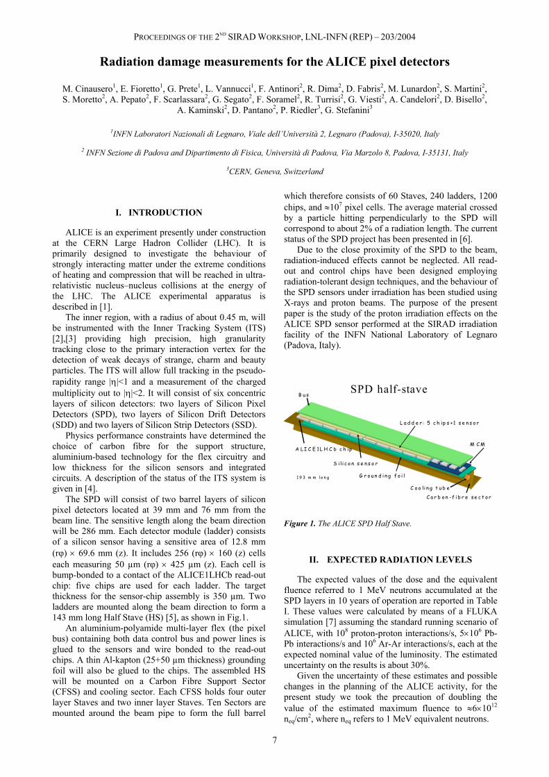
The SPD will consist of two barrel layers of silicon pixel detectors located at 39 mm and 76 mm from the beam line. The sensitive length along the beam direction will be 286 mm. Each detector module (ladder) consists of a silicon sensor having a sensitive area of 12.8 mm (rφ) × 69.6 mm (z). It includes 256 (rφ) × 160 (z) cells each measuring 50 µm (rφ) × 425 µm (z). Each cell is bump-bonded to a contact of the ALICE1LHCb read-out chip: five chips are used for each ladder. The target thickness for the sensor-chip assembly is 350 µm. Two ladders are mounted along the beam direction to form a 143 mm long Half Stave (HS) [5], as shown in Fig.1.
An aluminium-polyamide multi-layer flex (the pixel bus) containing both data control bus and power lines is glued to the sensors and wire bonded to the read-out chips. A thin Al-kapton (25+50 µm thickness) grounding foil will also be glued to the chips. The assembled HS will be mounted on a Carbon Fibre Support Sector (CFSS) and cooling sector. Each CFSS holds four outer layer Staves and two inner layer Staves. Ten Sectors are mounted around the beam pipe to form the full barrel
which therefore consists of 60 Staves, 240 ladders, 1200 chips, and ≈107 pixel cells. The average material crossed by a particle hitting perpendicularly to the SPD will correspond to about 2% of a radiation length. The current status of the SPD project has been presented in [6].
Due to the close proximity of the SPD to the beam, radiation-induced effects cannot be neglected. All read-out and control chips have been designed employing radiation-tolerant design techniques, and the behaviour of the SPD sensors under irradiation has been studied using X-rays and proton beams. The purpose of the present paper is the study of the proton irradiation effects on the ALICE SPD sensor performed at the SIRAD irradiation facility of the INFN National Laboratory of Legnaro (Padova, Italy).
C a r b o n -f i b r e se c t o r
G r o u n d i n g f o i l
SPD half-staveB u s
A LI C E 1 L H C b c h ip
C o o li n g t u b e
M C M
S i li c o n s e n s o r
L a d d e r : 5 c h ip s +1 s e n s o r
1 9 3 m m l o n g
Figure 1. The ALICE SPD Half Stave.
II. EXPECTED RADIATION LEVELS
The expected values of the dose and the equivalent fluence referred to 1 MeV neutrons accumulated at the SPD layers in 10 years of operation are reported in Table I. These values were calculated by means of a FLUKA simulation [7] assuming the standard running scenario of ALICE, with 108 proton-proton interactions/s, 5×10⁶ Pb-Pb interactions/s and 106 Ar-Ar interactions/s, each at the expected nominal value of the luminosity. The estimated uncertainty on the results is about 30%.
Given the uncertainty of these estimates and possible changes in the planning of the ALICE activity, for the present study we took the precaution of doubling the value of the estimated maximum fluence to ≈6×10¹² neq/cm2, where neq refers to 1 MeV equivalent neutrons.

PROCEEDINGS OF THE 2ND SIRAD WORKSHOP, LNL-INFN (REP) – 203/2004
8
TABLE I. IRRADIATION LEVEL OF THE SPD DETECTORS IN 10 YEARS OF ALICE ACTIVITY.
Dose (Gy(Si))
Dose (krad(Si))
Fluence (1 MeV equivalent n/cm2)
SPD layer 1 2.5×10³ 250 2.95×10¹² SPD layer 2 5.2×10² 52 1.30×10¹²
III. SPD SENSOR IRRADIATION
The SPD were irradiated at the SIRAD irradiation facility by a 27-MeV proton beam delivered from the Tandem-XTU accelerator of the INFN National Laboratory of Legnaro. The sensors were mounted on a mobile frame inside the vacuum chamber (see Fig.2) in order to easily change the devices exposed to the beam. The proton beam was rastered with uniformity of 7% on a 5×5 cm2 area. The flux during irradiation was set to ≈108-109 protons/(cm2×s).
The displacement damage is observed when atoms of the lattice structure are displaced from their original position by impinging particles on the silicon crystal. The sensor radiation damage was referred to the displacement damage induced by 1 MeV neutrons rescaling the fluences for 27 MeV protons to 1 MeV neutrons by the 27 MeV proton hardness factor K(p) calculated as follows:
( ) ∫∫ ⋅
=dE)E,p(S
dE)E,p(S)E,p(DnD
1)p(K (1)
where n and p indicate 1 MeV neutrons and 27 MeV protons, respectively, E is the energy, S is the energy spectrum, D is the displacement damage cross section, and D(n)=95 MeV×mb. The obtained value for the hardness factor of 27 MeV protons was K(p)≈2.
Figure 2. Scheme of the SIRAD irradiation facility.
IV. SPD DIODE CHARACTERIZATION
The radiation damage induces microscopic defects in the detector substrate, which cause variations of the sensor characteristics at macroscopic level. In particular, radiation-induced defects at midgap of the Si valence and conduction bands cause an increase of the leakage current; donor compensation and deep acceptor
generation by radiation produce variations of the depletion voltage; the electron-hole pair recombination and the trapping of charge carriers reduce the charge collection efficiency. For this reason the level of the radiation damage can be evaluated by the comparison of the leakage current and of the depletion voltage before and after irradiation.
Figure 3. Diode characterization at CERN.
TABLE II. DIODE CHARACTERIZATION IN PADOVA.
Idiode at Vbias=50 V
(nA)
Idiode at Vbias=100 V
(nA)
Temperature (°C)
Vdep (V)
1#1-63-p 100 2000 23.9 ≈29 1#2-68 5.5 401 24.2 ≈17 1#263p 6 6.9 24.1 ≈18
1#2-68#2 13.5 35.7 24.0 ≈17 1#2-63r 4.1 6.2 24.1 ≈18
1#2-63r#2 6.5 90.9 24.0 ≈18 1#2-63p#2 5.7 8.3 24.1 ≈20
All the sensors where electrically characterized
before irradiation. A first set of 7 diodes, with thickness of 300 µm, was wire-bonded in order to bias the devices during irradiation. For this reason the electrical characterization was performed at CERN before shipping (Fig.6), after wire-bonding in Padova (Table II), and finally also at the INFN National Laboratory of Legnaro by using a 241Am α source.
The results of the electrical characterizations before irradiation are mutually in agreement, showing low leakage currents (some nA) and depletion voltage Vdep≈20 V.
A second set of diodes, with thickness of 200 µm, was exposed unbiased to the proton beam, i.e. without wire-bonding. In this case the electrical characterization was performed by contacting the diodes with needles of a probing setup. The leakage current and the full depletion voltage of the 200 µm thick sensors, when rescaled for the different thickness, are similar to the values measured for the 300 µm thick devices.
PROCEEDINGS OF THE 2ND SIRAD WORKSHOP, LNL-INFN (REP) – 203/2004
9
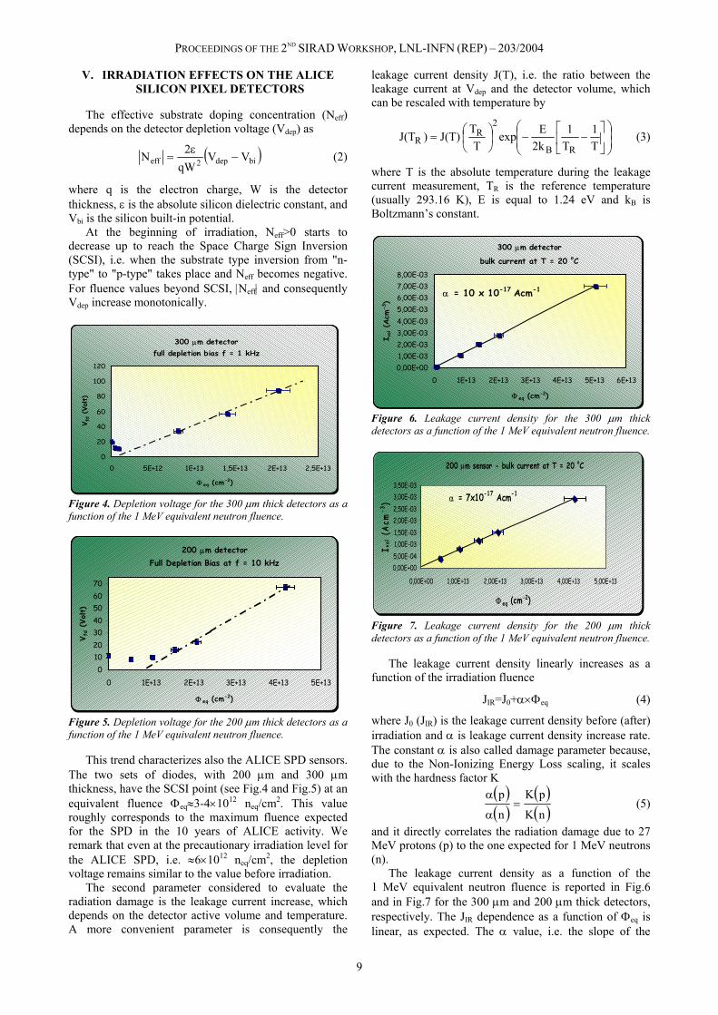
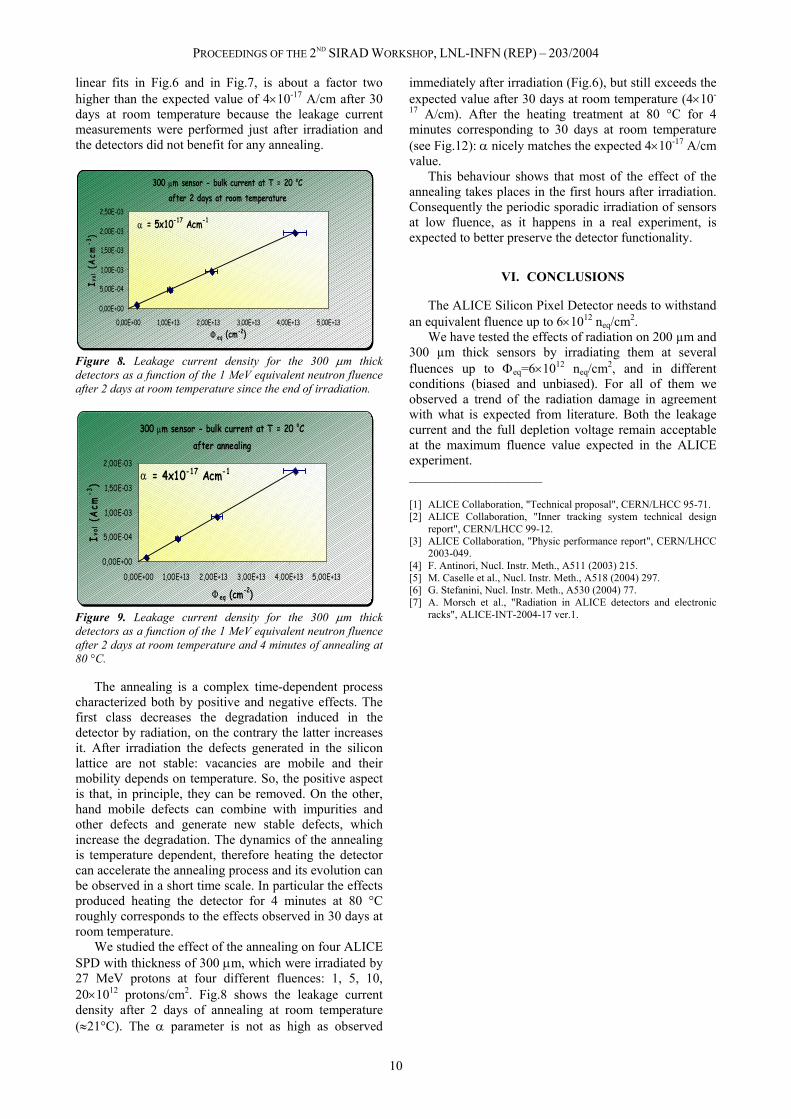
V. IRRADIATION EFFECTS ON THE ALICE SILICON PIXEL DETECTORS
The effective substrate doping concentration (Neff) depends on the detector depletion voltage (Vdep) as
( )bidep2eff VVqW
2N −ε
= (2)
where q is the electron charge, W is the detector thickness, ε is the absolute silicon dielectric constant, and Vbi is the silicon built-in potential.
At the beginning of irradiation, Neff>0 starts to decrease up to reach the Space Charge Sign Inversion (SCSI), i.e. when the substrate type inversion from "n-type" to "p-type" takes place and Neff becomes negative. For fluence values beyond SCSI, |Neff| and consequently Vdep increase monotonically.
300 µm detectorfull depletion bias f = 1 kHz
0
20
40
60
80
100
120
0 5E+12 1E+13 1,5E+13 2E+13 2,5E+13
Φ eq (cm-2)
V fd (V
olt)
Figure 4. Depletion voltage for the 300 µm thick detectors as a function of the 1 MeV equivalent neutron fluence.
200 µm detector Full Depletion Bias at f = 10 kHz
010203040506070
0 1E+13 2E+13 3E+13 4E+13 5E+13
Φ eq (cm-2)
V fd
(Volt)
Figure 5. Depletion voltage for the 200 µm thick detectors as a function of the 1 MeV equivalent neutron fluence.
This trend characterizes also the ALICE SPD sensors. The two sets of diodes, with 200 µm and 300 µm thickness, have the SCSI point (see Fig.4 and Fig.5) at an equivalent fluence Φeq≈3-4×10¹² neq/cm2. This value roughly corresponds to the maximum fluence expected for the SPD in the 10 years of ALICE activity. We remark that even at the precautionary irradiation level for the ALICE SPD, i.e. ≈6×10¹² neq/cm2, the depletion voltage remains similar to the value before irradiation.
The second parameter considered to evaluate the radiation damage is the leakage current increase, which depends on the detector active volume and temperature. A more convenient parameter is consequently the
leakage current density J(T), i.e. the ratio between the leakage current at Vdep and the detector volume, which can be rescaled with temperature by
⎟⎟⎠
⎞⎜⎜⎝
⎛⎥⎦
⎤⎢⎣
⎡−−⎟
⎠⎞
⎜⎝⎛=
T1
T1
2kEexp
TT J(T))J(T
RB
2R
R (3)
where T is the absolute temperature during the leakage current measurement, TR is the reference temperature (usually 293.16 K), E is equal to 1.24 eV and kB is Boltzmann’s constant.
300 µm detector
bulk current at T = 20 oC
α = 10 x 10-17 Acm-1
0,00E+001,00E-032,00E-033,00E-034,00E-035,00E-036,00E-037,00E-038,00E-03
0 1E+13 2E+13 3E+13 4E+13 5E+13 6E+13
Φ eq (cm-2)I v
ol (
Acm
-3)
Figure 6. Leakage current density for the 300 µm thick detectors as a function of the 1 MeV equivalent neutron fluence.
200 µm sensor - bulk current at T = 20 oC
α = 7x10-17 Acm-1
0,00E+005,00E-041,00E-031,50E-032,00E-032,50E-033,00E-033,50E-03
0,00E+00 1,00E+13 2,00E+13 3,00E+13 4,00E+13 5,00E+13
Φ eq (cm-2)
I vol (
Acm
-3)
Figure 7. Leakage current density for the 200 µm thick detectors as a function of the 1 MeV equivalent neutron fluence.
The leakage current density linearly increases as a function of the irradiation fluence
JIR=J0+α×Φeq (4)
where J0 (JIR) is the leakage current density before (after) irradiation and α is leakage current density increase rate. The constant α is also called damage parameter because, due to the Non-Ionizing Energy Loss scaling, it scales with the hardness factor K
( )( )
( )( )nK
pK
n
p=
α
α (5)
and it directly correlates the radiation damage due to 27 MeV protons (p) to the one expected for 1 MeV neutrons (n).
The leakage current density as a function of the 1 MeV equivalent neutron fluence is reported in Fig.6 and in Fig.7 for the 300 µm and 200 µm thick detectors, respectively. The JIR dependence as a function of Φeq is linear, as expected. The α value, i.e. the slope of the
PROCEEDINGS OF THE 2ND SIRAD WORKSHOP, LNL-INFN (REP) – 203/2004
10
linear fits in Fig.6 and in Fig.7, is about a factor two higher than the expected value of 4×10-17 A/cm after 30 days at room temperature because the leakage current measurements were performed just after irradiation and the detectors did not benefit for any annealing.
300 µm sensor - bulk current at T = 20 oC
after 2 days at room temperature
0,00E+00
5,00E-04
1,00E-03
1,50E-03
2,00E-03
2,50E-03
0,00E+00 1,00E+13 2,00E+13 3,00E+13 4,00E+13 5,00E+13Φ eq (cm-2)
I vol (
Acm
-3)
α = 5x10-17 Acm-1
Figure 8. Leakage current density for the 300 µm thick detectors as a function of the 1 MeV equivalent neutron fluence after 2 days at room temperature since the end of irradiation.
300 µm sensor - bulk current at T = 20 oCafter annealing
α = 4x10-17 Acm-1
0,00E+00
5,00E-04
1,00E-03
1,50E-03
2,00E-03
0,00E+00 1,00E+13 2,00E+13 3,00E+13 4,00E+13 5,00E+13
Φ eq (cm-2)
Ivol (
Acm
-3)
Figure 9. Leakage current density for the 300 µm thick detectors as a function of the 1 MeV equivalent neutron fluence after 2 days at room temperature and 4 minutes of annealing at 80 °C.
The annealing is a complex time-dependent process characterized both by positive and negative effects. The first class decreases the degradation induced in the detector by radiation, on the contrary the latter increases it. After irradiation the defects generated in the silicon lattice are not stable: vacancies are mobile and their mobility depends on temperature. So, the positive aspect is that, in principle, they can be removed. On the other, hand mobile defects can combine with impurities and other defects and generate new stable defects, which increase the degradation. The dynamics of the annealing is temperature dependent, therefore heating the detector can accelerate the annealing process and its evolution can be observed in a short time scale. In particular the effects produced heating the detector for 4 minutes at 80 °C roughly corresponds to the effects observed in 30 days at room temperature.
We studied the effect of the annealing on four ALICE SPD with thickness of 300 µm, which were irradiated by 27 MeV protons at four different fluences: 1, 5, 10, 20×1012 protons/cm2. Fig.8 shows the leakage current density after 2 days of annealing at room temperature (≈21°C). The α parameter is not as high as observed
immediately after irradiation (Fig.6), but still exceeds the expected value after 30 days at room temperature (4×10-
17 A/cm). After the heating treatment at 80 °C for 4 minutes corresponding to 30 days at room temperature (see Fig.12): α nicely matches the expected 4×10-17 A/cm value.
This behaviour shows that most of the effect of the annealing takes places in the first hours after irradiation. Consequently the periodic sporadic irradiation of sensors at low fluence, as it happens in a real experiment, is expected to better preserve the detector functionality.
VI. CONCLUSIONS
The ALICE Silicon Pixel Detector needs to withstand an equivalent fluence up to 6×10¹² neq/cm2.
We have tested the effects of radiation on 200 µm and 300 µm thick sensors by irradiating them at several fluences up to Φeq=6×10¹² neq/cm2, and in different conditions (biased and unbiased). For all of them we observed a trend of the radiation damage in agreement with what is expected from literature. Both the leakage current and the full depletion voltage remain acceptable at the maximum fluence value expected in the ALICE experiment. ____________________ [1] ALICE Collaboration, "Technical proposal", CERN/LHCC 95-71. [2] ALICE Collaboration, "Inner tracking system technical design
report", CERN/LHCC 99-12. [3] ALICE Collaboration, "Physic performance report", CERN/LHCC
2003-049. [4] F. Antinori, Nucl. Instr. Meth., A511 (2003) 215. [5] M. Caselle et al., Nucl. Instr. Meth., A518 (2004) 297. [6] G. Stefanini, Nucl. Instr. Meth., A530 (2004) 77. [7] A. Morsch et al., "Radiation in ALICE detectors and electronic
racks", ALICE-INT-2004-17 ver.1.

PROCEEDINGS OF THE 2ND SIRAD WORKSHOP, LNL-INFN (REP) – 203/2004
11
Development of Czochralski silicon particle detectors
J. Härkönen, P. Luukka, E. Tuovinen, E. Tuominen
Helsinki Institute of Physics, CERN Office, CERN/EP, CH-1211, Geneve 23, Switzerland
I. INTRODUCTION
Silicon detectors are widely used in High Energy Physics experiments because of their mature fabrication technology and favourable electrical properties. At the CERN Large Hadron Collider (LHC) experiments, detectors will be subjected to very hostile radiation environment. Unfortunately, this particle radiation causes irreversible crystallographic defects in silicon material thus inducing generation-recombination centres, which in turn result to an increase of the detector leakage current.
Additionally, crystallographic defects compensate the initial space charge of the silicon substrate [1], finally changing the conductivity from n- to p-type. Furthermore, silicon detectors are p-i-n diode structures designed to operate at full depletion with moderate reverse bias voltages (≈100-200 V). However, radiation induced defects lead to increase the depletion voltage. Thus, after high particle irradiation fluences, the breakdown voltage of the p-i-n structure may be reached before the full depletion.
High oxygen concentration demonstrably improves the radiation hardness of silicon detectors [2]. Particle detectors are traditionally processed on high resistivity Float Zone silicon (FZ-Si) that is fully depleted at reasonably low operating voltages but, on the other hand, has low oxygen concentration. FZ-Si can be oxygenated ([O]≈1017 cm-3) by long-term diffusion at high temperature. However, because of the contamination risk present in high temperature processes, the oxygenation is difficult to be implemented in large-scale production.
Recent developments in the crystal growth technology of Czochralski silicon (Cz-Si) have enabled the production of Cz-Si wafers with sufficiently high resistivity and with well-controlled high concentration of oxygen ([O]≈1018 cm-3). In addition, using Cz-Si as detector material may offer economical benefits. Since Cz-Si wafers are available up to the diameter of 300 mm, very large area detectors could be manufactured. This could bring significant savings in the costs related to detector front-end electronics and module assembly.
We have processed detectors on silicon wafers grown by Magnetic Czochralski (MCz) method. The MCz method has several advantages. It extends the controllable range of oxygen dissolving from the silica crucible during the crystal growth. A magnetic field can be applied in the crystal growth system in order to damp the oscillations in the melt. The applied field creates an electric current distribution and an induced magnetic field in the electrically conducting melt. This produces a Lorentz force that influences the flow and reduces the amplitude of the melt fluctuations [3]. The n- and p-type Cz-Si wafers manufactured by Okmetic Ltd (Finland) have a nominal resistivity of ≈900 Ω×cm and ≈2000
Ω×cm for n- and p-type silicon, respectively. The oxygen concentration is less than 10 atomic part per million (ppma).
II. DETECTOR PROCESSING
The high resistivity Cz-Si detectors can basically be processed into segmented or pad detectors in the same way as in the case of the traditionally used Fz-Si substrates. The process sequence is described in detail in [4]. The essential difference between Cz-Si and Fz-Si materials is, however, the oxygen concentration. It is well know that the aggregation of oxygen atoms will lead to the formation of electrically active defects, commonly named Thermal Donors (TD) [5-7]. The TDs are shallow donor levels within the energy range of 0.01-0.2 eV below the conduction band [8]. The formation of thermal donors is strongly dependent on the temperature and on the oxygen concentration in the silicon material. Heat treatment between 400-600 °C can yield to a TD concentration comparable to that of the background doping of high resistivity magnetic Cz-Si and thus to significant deviation in the full depletion voltages of the detectors. It has also been found that the presence of hydrogen in the detector fabrication process can enhance the generation of TDs [9].
The TD generation can be formulated by the empirical equation [10]
⎭⎬⎫
⎩⎨⎧ −−
−⎟⎠⎞
⎜⎝⎛= ⋅⋅⋅χ tioCiDb
2Ad
ioTD e1NN
1CbaN (1)
where a and b are experimental fitting parameters, Cio is the concentration of interstitial oxygen in silicon, χ is a constant (2<χ<3), Nd-NA is the free carrier concentration, and t is the time at a given temperature. Di is the diffusion constant of interstitial oxygen given by
⎟⎟⎠
⎞⎜⎜⎝
⎛−
×=kTE
e13.0D
A
i (2) where EA is the activation energy, k is Bolzmann’s constant and T is the absolute temperature. The EA value of 2.53 eV for the activation energy can be found in [10]. The model presented in (1) is based on the assumption that the TD formation kinetics is limited by the diffusion of interstitial oxygen.
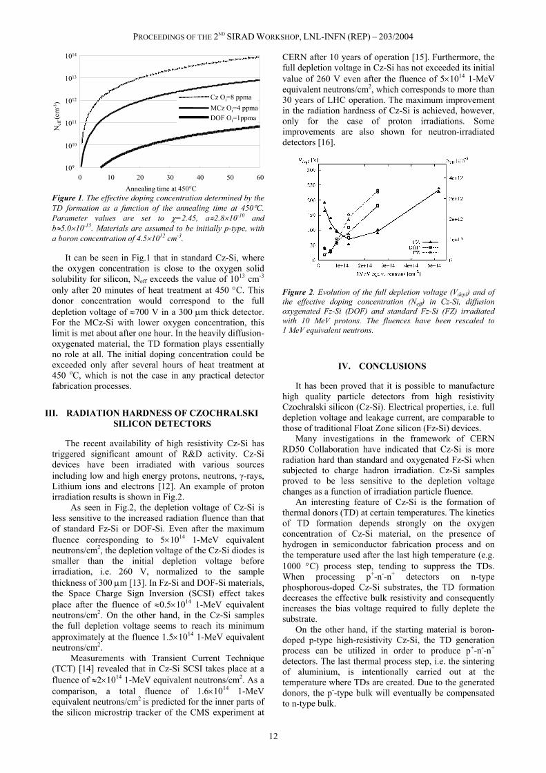
The TD generation in different oxygen rich detector materials can be roughly estimated by applying values reported in literature for the parameters in (1) and (2). Calculations were performed for standard Cz-Si (Oi≈8 ppma), for Cz-Si grown with magnetic field (Oi≈4 ppma) and for high-temperature long-time (HTLT) diffusion oxygenated Fz-Si (Oi≈1 ppma) [11]. The effective doping concentration determined by the TD formation as a function of annealing time at 450 °C is shown in Fig.1.
PROCEEDINGS OF THE 2ND SIRAD WORKSHOP, LNL-INFN (REP) – 203/2004
12
109
1010
1011
1012
1013
1014
0 10 20 30 40 50 60Annealing time at 450°C
Cz Oi=8 ppmaMCz Oi=4 ppmaDOF Oi=1ppma
Cz Oi=8 ppmaMCz Oi=4 ppmaDOF Oi=1ppma
Nef
f (cm
-3)
Figure 1. The effective doping concentration determined by the TD formation as a function of the annealing time at 450°C. Parameter values are set to χ=2.45, a≈2.8×10⁻¹⁰ and b≈5.0×10⁻¹⁵. Materials are assumed to be initially p-type, with a boron concentration of 4.5×1012 cm-3.
It can be seen in Fig.1 that in standard Cz-Si, where the oxygen concentration is close to the oxygen solid solubility for silicon, Neff exceeds the value of 1013 cm-3 only after 20 minutes of heat treatment at 450 °C. This donor concentration would correspond to the full depletion voltage of ≈700 V in a 300 µm thick detector. For the MCz-Si with lower oxygen concentration, this limit is met about after one hour. In the heavily diffusion-oxygenated material, the TD formation plays essentially no role at all. The initial doping concentration could be exceeded only after several hours of heat treatment at 450 oC, which is not the case in any practical detector fabrication processes.
III. RADIATION HARDNESS OF CZOCHRALSKI SILICON DETECTORS
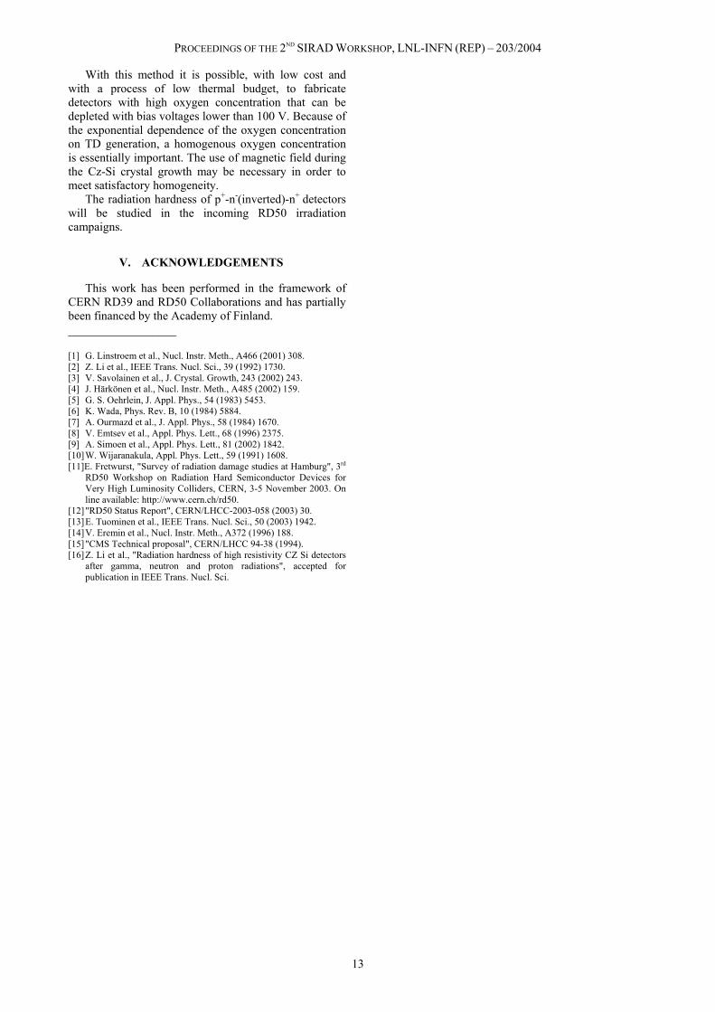
The recent availability of high resistivity Cz-Si has triggered significant amount of R&D activity. Cz-Si devices have been irradiated with various sources including low and high energy protons, neutrons, γ-rays, Lithium ions and electrons [12]. An example of proton irradiation results is shown in Fig.2.
As seen in Fig.2, the depletion voltage of Cz-Si is less sensitive to the increased radiation fluence than that of standard Fz-Si or DOF-Si. Even after the maximum fluence corresponding to 5×10¹⁴ 1-MeV equivalent neutrons/cm2, the depletion voltage of the Cz-Si diodes is smaller than the initial depletion voltage before irradiation, i.e. 260 V, normalized to the sample thickness of 300 µm [13]. In Fz-Si and DOF-Si materials, the Space Charge Sign Inversion (SCSI) effect takes place after the fluence of ≈0.5×10¹⁴ 1-MeV equivalent neutrons/cm2. On the other hand, in the Cz-Si samples the full depletion voltage seems to reach its minimum approximately at the fluence 1.5×10¹⁴ 1-MeV equivalent neutrons/cm2.
Measurements with Transient Current Technique (TCT) [14] revealed that in Cz-Si SCSI takes place at a fluence of ≈2×10¹⁴ 1-MeV equivalent neutrons/cm2. As a comparison, a total fluence of 1.6×10¹⁴ 1-MeV equivalent neutrons/cm2 is predicted for the inner parts of the silicon microstrip tracker of the CMS experiment at
CERN after 10 years of operation [15]. Furthermore, the full depletion voltage in Cz-Si has not exceeded its initial value of 260 V even after the fluence of 5×10¹⁴ 1-MeV equivalent neutrons/cm2, which corresponds to more than 30 years of LHC operation. The maximum improvement in the radiation hardness of Cz-Si is achieved, however, only for the case of proton irradiations. Some improvements are also shown for neutron-irradiated detectors [16].
Figure 2. Evolution of the full depletion voltage (Vdepl) and of the effective doping concentration (Neff) in Cz-Si, diffusion oxygenated Fz-Si (DOF) and standard Fz-Si (FZ) irradiated with 10 MeV protons. The fluences have been rescaled to 1 MeV equivalent neutrons.
IV. CONCLUSIONS
It has been proved that it is possible to manufacture high quality particle detectors from high resistivity Czochralski silicon (Cz-Si). Electrical properties, i.e. full depletion voltage and leakage current, are comparable to those of traditional Float Zone silicon (Fz-Si) devices.
Many investigations in the framework of CERN RD50 Collaboration have indicated that Cz-Si is more radiation hard than standard and oxygenated Fz-Si when subjected to charge hadron irradiation. Cz-Si samples proved to be less sensitive to the depletion voltage changes as a function of irradiation particle fluence.
An interesting feature of Cz-Si is the formation of thermal donors (TD) at certain temperatures. The kinetics of TD formation depends strongly on the oxygen concentration of Cz-Si material, on the presence of hydrogen in semiconductor fabrication process and on the temperature used after the last high temperature (e.g. 1000 °C) process step, tending to suppress the TDs. When processing p+-n--n+ detectors on n-type phosphorous-doped Cz-Si substrates, the TD formation decreases the effective bulk resistivity and consequently increases the bias voltage required to fully deplete the substrate.
On the other hand, if the starting material is boron-doped p-type high-resistivity Cz-Si, the TD generation process can be utilized in order to produce p+-n--n+ detectors. The last thermal process step, i.e. the sintering of aluminium, is intentionally carried out at the temperature where TDs are created. Due to the generated donors, the p--type bulk will eventually be compensated to n-type bulk.
PROCEEDINGS OF THE 2ND SIRAD WORKSHOP, LNL-INFN (REP) – 203/2004
13
With this method it is possible, with low cost and with a process of low thermal budget, to fabricate detectors with high oxygen concentration that can be depleted with bias voltages lower than 100 V. Because of the exponential dependence of the oxygen concentration on TD generation, a homogenous oxygen concentration is essentially important. The use of magnetic field during the Cz-Si crystal growth may be necessary in order to meet satisfactory homogeneity.
The radiation hardness of p+-n-(inverted)-n+ detectors will be studied in the incoming RD50 irradiation campaigns.
V. ACKNOWLEDGEMENTS
This work has been performed in the framework of CERN RD39 and RD50 Collaborations and has partially been financed by the Academy of Finland. __________________ [1] G. Linstroem et al., Nucl. Instr. Meth., A466 (2001) 308. [2] Z. Li et al., IEEE Trans. Nucl. Sci., 39 (1992) 1730. [3] V. Savolainen et al., J. Crystal. Growth, 243 (2002) 243. [4] J. Härkönen et al., Nucl. Instr. Meth., A485 (2002) 159. [5] G. S. Oehrlein, J. Appl. Phys., 54 (1983) 5453. [6] K. Wada, Phys. Rev. B, 10 (1984) 5884. [7] A. Ourmazd et al., J. Appl. Phys., 58 (1984) 1670. [8] V. Emtsev et al., Appl. Phys. Lett., 68 (1996) 2375. [9] A. Simoen et al., Appl. Phys. Lett., 81 (2002) 1842. [10] W. Wijaranakula, Appl. Phys. Lett., 59 (1991) 1608. [11]E. Fretwurst, "Survey of radiation damage studies at Hamburg", 3rd
RD50 Workshop on Radiation Hard Semiconductor Devices for Very High Luminosity Colliders, CERN, 3-5 November 2003. On line available: http://www.cern.ch/rd50.
[12] "RD50 Status Report", CERN/LHCC-2003-058 (2003) 30. [13] E. Tuominen et al., IEEE Trans. Nucl. Sci., 50 (2003) 1942. [14] V. Eremin et al., Nucl. Instr. Meth., A372 (1996) 188. [15] "CMS Technical proposal", CERN/LHCC 94-38 (1994). [16] Z. Li et al., "Radiation hardness of high resistivity CZ Si detectors
after gamma, neutron and proton radiations", accepted for publication in IEEE Trans. Nucl. Sci.

PROCEEDINGS OF THE 2ND SIRAD WORKSHOP, LNL-INFN (REP) – 203/2004
14
Development of a fabrication technology for PIN diodes on thinned silicon substrate
S. Ronchin1, M. Boscardin1, G.-F. Dalla Betta2, P. Gregori1, V. Guarnieri1, C. Piemonte1, N. Zorzi1
1ITC-irst, Divisione Microsistemi, Via Sommarive 18, Povo (Trento), I-38050, Italy
2Dipartimento di Informatica e Telecomunicazioni, Università di Trento, Povo (Trento), I-38050, Italy
I. INTRODUCTION
In the last ten years, an extensive research activity in the field of silicon radiation detectors has been strongly focused on the strict requirements of the future CERN-LHC (Large Hadron Collider). The detectors, to be used for these experiments, will be exposed to very high fluences of particles in the 10 years of operation, with a foreseen luminosity of about 1034 cm-2×s-1, resulting in a consequent performance degradation. Radiation damage induces several detrimental effects on high resistivity silicon detectors [1],[2], among them, the growth of the full depletion voltage after substrate type inversion is of particular concern. The usage of very thin detectors is one possible strategy in order to face this problem. The direct advantage of such approach is the reduced depletion voltage even after high irradiation fluences. Moreover, the starting resistivity of a thin sensor can be much lower than standard devices with 300 µm thickness, preserving a low depletion voltage (100-200 V) and, as a consequence, the type inversion can be delayed to higher irradiation fluences. Finally, an improvement of the tracking precision and momentum resolution is expected.
Thin diode detectors have been already employed in many applications such as ∆E-E telescopes for heavy ion detection and tracking [3]-[5], short range particle detection under high γ-ray background [4], X-ray (E>10 keV) beam monitoring [4], and in all the applications where high radiation selectivity, short particle path and reduced multiple scattering of charged particles are required [3]-[6].
Very thin silicon wafers (< 200 µm) cannot be easily handled by the standard equipment used in fabrication lines. Thus, a mechanical lapping cannot be used to thin the wafers down to the required depth (50-100 µm). The most convenient approach is a local thinning adopting the technology used for micro-machined sensors, based on dry or wet etching. Several techniques are available [7], among them the wet anisotropic silicon etchant TMAH (Tetra-Methyl Ammonium Hydroxide) has recently gained considerable interest because of the CMOS process compatibility. Furthermore, the TMAH shows a very good etching uniformity and a relatively high selectivity for silicon with respect to oxides and nitrides at some fixed TMAH weight-% (wt%) concentrations [8].
The aim of this work is to show the feasibility of thin detectors satisfying the requirements for the new generation detectors. In particular, we report on the
development of a fabrication technology for the realization of PIN diodes on membranes obtained by locally thinning the silicon substrate by means of TMAH etching from the wafer backside. Diodes of different shapes and sizes have been fabricated on 50 µm and 100 µm thick membranes. They have been tested, showing a low leakage current (≈2 nA/cm2 for the 50 µm membrane) and, as expected, a very low depletion voltage (≈1 V).
II. FABRICATION PROCESS
The fabrication process of a detector on a thin silicon membrane is based on a pre-existent technology developed at ITC-irst for PIN diodes, adding the etching step of the wafer backside. In particular, the silicon etching is performed using a solution with a concentration of 25 wt% of TMAH at a temperature of 90 °C.
Fig.1 shows the schematic flowchart of the fabrication process that requires 5 mask steps: 4 on the front side and one to define the membranes on the backside.
Figure 1. Schematic process flow for the fabrication of a thin diode on n-type substrate.

PROCEEDINGS OF THE 2ND SIRAD WORKSHOP, LNL-INFN (REP) – 203/2004
15
The main characteristics of the silicon wafers for device processing are: 100 mm diameter, Floating Zone (FZ), 300 µm thick, <100> oriented, phosphorus doped with 6 kΩ×cm nominal resistivity. We have etched two groups of wafers for different times obtaining two different silicon membrane thickness of ≈50 µm and ≈100 µm, respectively, as reported in Table I: the wafer thickness was measured by a micrometer and the etching depth by a microscope comparator. Fig.2 shows, as an example, the SEM photograph of the cross section for a thinned region.
It is worthwhile to note that on the wafers treated with TMAH there are also some devices that have not been etched. In addition, two wafers are processed without the TMAH etching as a reference for the electrical characterization.
TABLE I. TMAH-ETCHED WAFERS.
Wafer number
Wafer thickness (µm)
Etching depth (µm)
Membrane thickness
(µm) 3 296±2 191±2 105±3 4 298±7 199±1 99±7 5 295±1 196±2 99±2 6 296±8 239±2 57±8 7 302±3 245±3 57±4 8 300±3 201±1 99±3 9 306±6 257±2 49±6
Figure 2. SEM photograph of a cross section for a silicon membrane obtained with TMAH etching. The white line indicates 1 mm.
(a) (b)
Figure 3. Layout of two different types of produced diodes: a) round diode with area of 2.27 mm2 and double guard-ring (FP20); b) square diodes of various areas : 0.75, 1.9, 3.5, 11.35 and 19.1 mm2 with single guard-ring.
III. DEVICE DESCRIPTION
We adopted in this process a wafer layout previously employed to the production of PIN diodes with different
active areas and shapes (see an example in Fig.3). A new mask has been added for the definition of the backside areas to be thinned. Being the etching angle for <100> silicon of 54.74°, one has to carefully oversize the holes in order to fabricate the device entirely inside the thinned region. In order to monitor the main parameters characterizing the fabrication technology, a set of standard test structures (diodes, MOS capacitors, gated diodes) is included.
IV. ELECTRICAL CHARACTERIZATION
IV.A. Technological Parameters
First, we compared the parameters extracted from 300 µm thick test structures from wafers processed with and without TMAH etching step, in order to evaluate the effects of the TMAH etchant on the electrical characteristics. The results, grouped by reference and TMAH-treated wafers, are summarized in Table II. Since no significant differences are observed in the values obtained for the two groups of wafers, we conclude that the TMAH treatment does not induce any damaging effect on the electrical parameters of the devices.
TABLE II. COMPARISON OF THE MAIN ELECTRICAL PARAMETERS MEASURED ON 300 µm THICK TEST STRUCTURES ON WAFERS
PROCESSED WITH AND WITHOUT TMAH ETCHING. VFD, ND, J AND τg ARE EXTRACTED FROM TEST DIODES. TOX, QOX, VFB ARE OBTAINED FROM
MOS CAPACITORS WITH THE ISOLATION OXIDE AS DIELECTRIC. s0 IS EVALUATED ON GATE CONTROLLED DIODES.
Reference TMAH-treated Full depletion voltage VFD (V) 17.6 13.5 Doping concentration ND (1011 cm-3) 2.6 2.0 Leakage current density J (nA/cm2) 2.7 2.2 Carrier generation lifetime τg (ms) 18 22 Oxide thickness TOX (nm) 438 437 Oxide charge density QOX (1010 cm-2) 1.4 1.4 Flatband voltage VFB (V) 0.77 0.77 Surface generation velocity s0 (cm/s) 2.5 3.0
IV.B. Characteristics of the Thinned Diodes
TMAH-etched wafers have been electrically characterized by capacitance-voltage (C-V) and current-voltage (I-V) measurements on devices manufactured both on the thinned membranes and on the full thickness bulk.
As an example, the 1/C2-V characteristics for 300 µm, 100 µm and 50 µm thick FP20 diodes are reported in Fig.4. The full depletion voltage of these devices is 13 V, 1 V and lower than 1 V, respectively.
Fig.5 exhibits the doping profiles, extracted by C-V measurements performed on FP20 diodes: the calculated thicknesses are very close to the previously measured data reported in Table I for the wafer numbers 4 and 6.
Fig.6 shows the guard-ring currents of several thinned devices having different thicknesses. These data refer to diodes having an area of 1.9 mm2. As expected, the guard-ring currents are very similar for all devices having the same thickness. It is worthwhile to note that the guard-ring current does not show any breakdown within a bias voltage of 100 V.

PROCEEDINGS OF THE 2ND SIRAD WORKSHOP, LNL-INFN (REP) – 203/2004
16
0.0
0.2
0.4
0.6
0.8
1.0
1.2
1.4
0 5 10 15 20 25Reverse Bias [V]
C-2
[pF-2
]
0.00
0.05
0.10
0.15
0.20
0 1 2 3
Figure 4. 1/C2-V characteristics for FP20 diodes: 300 µm (dotted lines), 100 µm (thick line) and 50 µm (thin line) thick devices. The inset shows a magnification at low voltages.
0.00.51.01.52.02.53.03.54.04.55.0
0 50 100 150 200 250 300
Depth [µm]
Dop
ing
[1012
· cm
-3]
Figure 5. Doping profiles for FP20 diodes: 300 µm (dotted lines), 99 µm (thick line) and 50 µm (thin line) thick devices.
0.0
0.2
0.4
0.6
0.8
0 50 100
Rev. Bias [V]
Iguar
d [n
A]
Figure 6. Guard-ring currents for the square diodes of 1.9 mm2 area: 300 µm (dashed lines), 100 µm (continuous lines) and 50 µm (dotted lines) thick diodes.
In Fig.7 a comparison between the diode current densities of thin and non-thinned devices is shown. The diodes show a low leakage current density at 100 V of ≈3 nA/cm2 for 100 µm and 2.1 nA/cm2 for 50 µm thick devices. These values are much lower than the ones reported in [4],[5],[9],[10], and comparable to that reported in [3], where the devices are obtained using a similar process.
The average leakage current at 100 V and the average full depletion voltage, measured on square PIN diodes of 1.9 mm2 area, are reported in Table III. It is interesting to observe that the values for the etched devices are lower than expected. Indeed, as the generation volumes of the etched devices are about 1/3 and 1/6 of the 300 µm thick ones, also the currents should respect these ratios.
Instead, in our cases, ratios of about 1/5 and 1/8 are observed, respectively. A possible explanation can be a more efficient gettering of impurities for thin membranes.
Nevertheless, the thinned diodes show a leakage current weakly dependent on the thickness. It may be ascribed to the fact that the bulk component of the current is so small that the surface contribution becomes dominant. This is appreciable also from the marked slope of the current after full depletion.
0
5
10
15
20
0 50 100
Rev. Bias [V]
Jlea
k [n
A/c
m2 ]
Figure 7. Leakage current density measured on square PIN diodes of 1.9 mm2 area: 300 µm (dashed lines), 100 µm (continuous lines) and 50 µm (dotted lines) thick diodes.
TABLE III. SUMMARY OF THE ELECTRICAL CHARACTERIZATION OF THE SQUARE PIN DIODES WITH 1.9 mm2 AREA.
Device thickness (µm)
Leakage current at 100 V (nA/cm2)
Full depletion voltage (V)
300 16±1 22
100 3.0±0.4 2.2
50 2.1±0.2 1.2
V. CONCLUSIONS
TMAH-etching is a suitable technique for producing thin PIN diode detectors. We have produced samples on ≈50 µm thick membranes having a full depletion voltage of ≈1 V and a leakage current close to 2 nA/cm2 at 100 V. Moreover, no breakdown up to 100 V is noticed and no differences in the technological parameters of TMAH-treated wafers with respect to wafers processed without silicon etching are observed.
Radiation damage characterization on samples irradiated with 58 MeV Li ions and charge collection efficiency measurements are in progress. ____________________ [1] M. Moll, Nucl. Instr. Meth., A511 (2003) 97. [2] M. Bruzzi, IEEE Trans. Nucl. Sci., 48 (2001) 960. [3] L. Evensen et al., IEEE Trans. Nucl. Sci., 44 (1997) 629. [4] F. Foulon et al., IEEE Trans. Nucl. Sci., 46 (1999) 218. [5] L. Stab, Nucl. Instr. Meth., A288 (1990) 24. [6] R. Horisberger, Nucl. Instr. Meth., A288 (1990) 87. [7] A. Faes et al., "Electrochemical effects during anisotropic bulk-
silicon etching with doped and undoped TMAH solutions", Proceedings of the 6th Italian Conference on Sensors and Microsystems, Pisa (Italy), 5-7 February 2001, World Scientific (2002) 276.
[8] T. A. Kovacs et al., Proceedings of the IEEE, 86-8 (1998) 1536. [9] L. Lavergne-Gosselin et al., Nucl. Instr. Meth., A276 (1989) 210. [10] P. Golubev et al., Nucl. Instr. Meth., A500 (2003) 96.
PROCEEDINGS OF THE 2ND SIRAD WORKSHOP, LNL-INFN (REP) – 203/2004
17
Radiation hardness of different silicon materials after high-energy electron irradiation
S. Dittongo1,2, L. Bosisio1,2, M. Ciacchi1, D. Contarato3,4, G. D’Auria5, E. Fretwurst4, G. Lindström4
1Dipartimento di Fisica, Università di Trieste, Via A. Valerio 2, Trieste, I-34127, Italy
2INFN Sezione di Trieste, Area di Ricerca, Padriciano 99, Trieste, I-34012, Italy
3DESY, Notkestrasse 85, Hamburg, D-22607, Germany
4Institut für Experimentalphysik, Universität Hamburg, Luruper Chaussee 149, Hamburg, D-22761, Germany
5Sincrotrone Trieste S.C.p.A., Area di Ricerca, Basovizza, Trieste, I-34012, Italy
I. INTRODUCTION
Silicon detectors are widely employed in High Energy Physics experiments operating at high luminosity hadron and lepton colliders. They are an even more important component of the experiments under construction for the very high luminosity LHC proton collider. In addition, they are foreseen to be extensively used in experiments at future machines such as second-generation b-factories and linear electron-positron colliders. For most of these applications the detector survival after years of operation in a harsh radiation environment is an essential requirement.
In recent years much effort has been devoted to the study of the radiation hardness of silicon detectors against neutrons, charged hadrons and γ-rays, and to the study of the improvements possibly achievable by using different silicon substrate materials. Extensive investigations have been performed by irradiating detectors, test structures and raw materials with different particle types, in particular charged hadrons (pions and protons) and neutrons [1]. Several studies have also been conducted with γ-rays [2],[3]. By contrast, very few contributions have been devoted to the study of the damage produced by high-energy (GeV) electrons in silicon. Previous results, obtained with 500 and 900 MeV electron irradiation of silicon devices fabricated on high resistivity Float Zone material, have shown that high-energy electrons, like neutrons and protons, are very effective in creating bulk damage in silicon [4]-[6]. In a recent work, extending the study to oxygen enriched silicon substrates [7], no significant effect of oxygen has been observed up to an electron fluence of ≈5×10¹⁴ e/cm2.
In the following we summarize the results of recent studies, extending these investigations to a wider range of substrate materials and to higher fluence levels up to 2.1×10¹⁵ e/cm2.
II. DEVICES AND EXPERIMENTAL CONDITIONS
Tested devices are p+/n-/n+ diodes fabricated on different silicon substrates, namely standard (StFZ) and
oxygenated (DOFZ) Float Zone, Czochralski (CZ) and epitaxial (EPI) silicon.
A set of standard and oxygenated Float Zone devices has been manufactured by CiS (Erfurt, Germany) on Wacker <111> substrates of typical resistivity of 3-4 kΩ×cm. Oxygen diffusion for DOFZ devices has been performed in an N2 environment for 72 hours at 1150 °C. A second set of StFZ diodes has been fabricated by ITC-irst (Trento, Italy) on high purity wafers from Topsil, with a resistivity of 10-20 kΩ×cm. Some of the substrates have been previously converted to DOFZ by a 12 hour oxidation at 1150 °C followed by a 36 hour diffusion in N2 at the same temperature, resulting in an oxygen concentration of 1-3×1017 cm-3 across the substrate.
Czochralski and epitaxial devices have also been processed by CiS. CZ diodes are manufactured on <100> wafers of resistivity 1.2 kΩ×cm from Sumitomo; EPI diodes are processed on a 50 µm thick epitaxial layer (resistivity 50 Ω×cm) grown by ITME (Warsaw, Poland) on a 300 µm thick low-resistivity (0.015 Ω×cm) Czochralski <111> substrate.
The active area of all CiS diodes is 0.5×0.5 cm2, while those fabricated by ITC-irst have an area of 0.35×0.35 cm2. All diodes are provided with a 100 µm wide guard-ring (which was grounded during the measurements), surrounded by a number of several floating rings. The substrate thickness for all devices is ≈300 µm.
Eight different irradiation steps up to a fluence of 2.1×10¹⁵ e/cm2 were performed with the 900 MeV electron beam of the LINAC injector at the synchrotron light facility Elettra in Trieste (Italy). Devices were kept unbiased during irradiation, at the ambient temperature of the LINAC (25 °C). Irradiated samples were electrically characterized by current-voltage (I-V) and capacitance-voltage (C-V) measurements, performed one day after irradiation and then after several thermal annealing cycles at 80 °C. The laboratory temperature during the measurements varied between 22 °C and 24 °C. All the measured currents have been normalized to 20 °C. Between irradiation and measurements the samples were kept at room temperature. After the first series of measurements, devices were stored at about -4 °C. The C-V measurements were performed at the 10 kHz frequency and the depletion voltage has been determined
PROCEEDINGS OF THE 2ND SIRAD WORKSHOP, LNL-INFN (REP) – 203/2004
18
from the saturation of the 1/C2-V or of the log(C)-log(V) curves.
III. EXPERIMENTAL RESULTS
III.A. Effective Doping Concentration
The values of the substrate effective doping concentration Neff, defined as the difference between the concentration of positively charged donors and the concentration of negatively charged acceptors, have been calculated for all devices from the measured values of the depletion voltage Vdep, according to the standard expression valid in the depletion approximation and for uniform doping
Vdqεε2
N dep20
0seff = (1)
where εs=11.8 is the relative dielectric constant of silicon, ε0=8.854×10⁻¹⁴ F/cm is the permittivity of vacuum, q0=1.602×10⁻¹⁹ C is the electron charge and d is the substrate thickness, evaluated for each device from the saturation value of the diode capacitance above full depletion voltage. All the reported data refer to devices annealed for 8 minutes at 80 °C, corresponding to the minimum in the radiation-induced change of the substrate effective doping concentration [8].
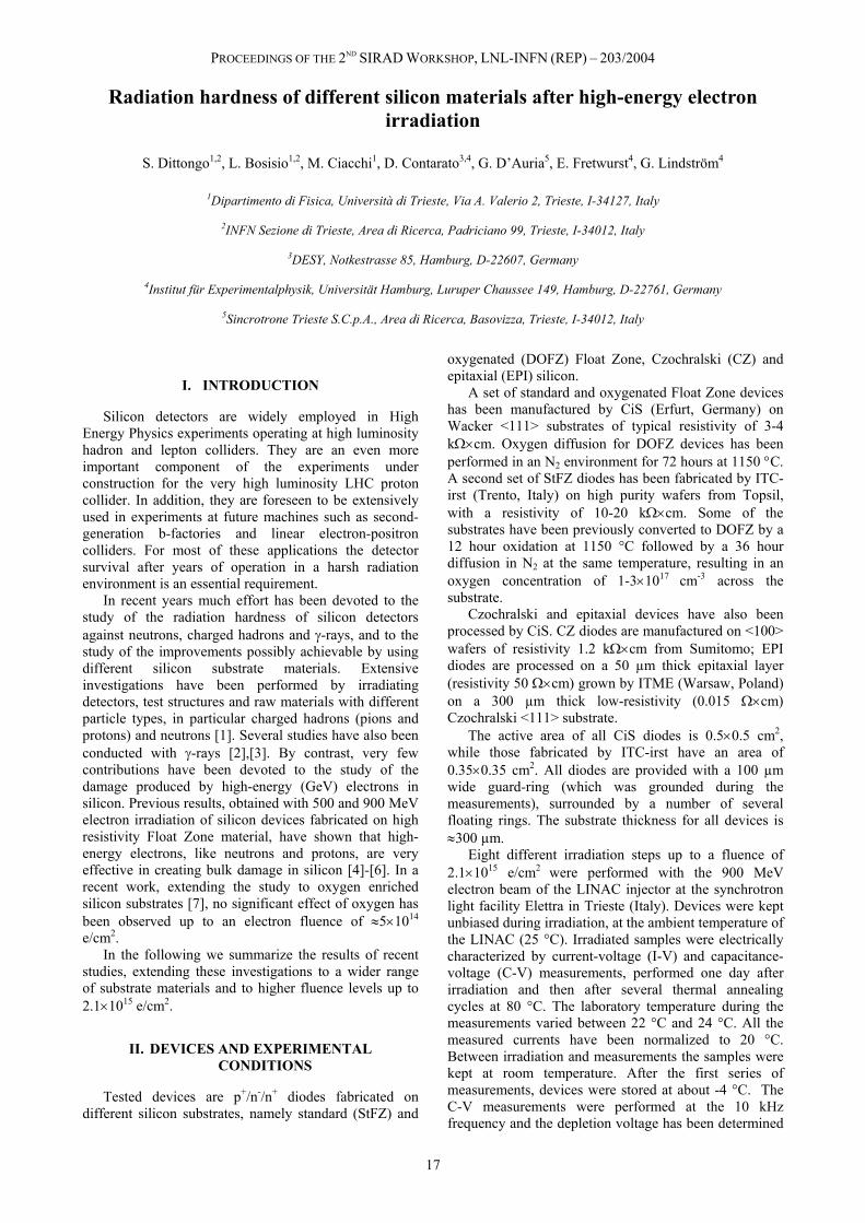
Fig.1 shows the values of Neff as a function of the electron fluence for StFZ and DOFZ devices. Substrate type inversion is observed for all devices, confirming that high-energy electrons are quite effective in creating bulk damage in silicon, as reported in [5]-[7]. Type inversion appears at ≈2.5×10¹⁴ e/cm2 for the ITC-irst devices fabricated on higher resistivity material and at ≈5×10¹⁴ e/cm2 for the CiS devices. After substrate type inversion, the slope of Neff as a function of the electron fluence is about -1.0×10⁻³ cm-1 for ITC-irst StFZ devices, -1.3×10⁻³ cm-1 for CiS StFZ diodes, -0.6×10⁻³ cm-1 for ITC-irst DOFZ structures and -0.5×10⁻³ cm-1 for CiS DOFZ devices. A lower slope appears to be associated with DOFZ substrates. Differences between diodes fabricated by ITC-irst and by CiS could be due to different starting materials and oxygen diffusion treatments. Similar results were also observed after charged hadron irradiation [1].
Within the considered electron fluence range, substrate type inversion is not observed for CZ and EPI devices, as shown in Fig.2, where Neff is normalized to the pre-irradiation value. For EPI devices, the absolute variations in Neff are of the same order of magnitude (≈1012 cm-3) as for the other materials. Nevertheless, thanks to the higher initial doping concentration, the relative changes in Neff are quite small and comparable with the uncertainty in the evaluation of the depletion voltage. Substrate type inversion is not even approached at the fluences considered, in agreement with what already observed after irradiation with 24 GeV/c protons [9],[10], where an initial decrease in Neff is followed by a moderate increase at higher fluences. For these reasons we consider our present measurements on EPI devices as
an intermediate step towards heavier irradiations, from which a clearer trend should emerge.
-2
-1
0
1
0 5.0×10¹⁴ 1.0×10¹⁵ 1.5×10¹⁵ 2.0×10¹⁵ 2.5×10¹⁵
Electron fluence (e/cm2)
Nef
f(1
012/c
m3)
StFZ-CiSDOFZ-CiSStFZ(111)-irstStFZ(100)-irstDOFZ(111)-irst
Figure 1. Effective doping concentration for StFZ and DOFZ devices measured after 8 minutes of thermal annealing at 80 °C.
0.5
0.6
0.7
0.8
0.9
1.0
1.1
0 5.0×10¹⁴ 1.0×10¹⁵ 1.5×10¹⁵ 2.0×10¹⁵ 2.5×10¹⁵
Electron fluence (e/cm2)
Nef
f /
Nef
f,0
EPI Set1
EPI Set2
CZ
Figure 2. Effective doping concentration for CZ and EPI devices measured after 8 minutes of thermal annealing at 80 °C, normalized to the value before irradiation.
For CZ devices the experimental curve of Neff appears instead to be approximately linear as a function of the electron fluence, with a slope of about -1.0×10⁻³ cm-1; a simple extrapolation of this trend would suggest that substrate type inversion could occur at a fluence of ≈4.5×10¹⁵ e/cm2, corresponding to a Non-Ionizing Energy Loss (NIEL) equivalent fluence of ≈3.6×10¹⁴ 1-MeV neutrons/cm2 [11], a value not far to the one reported in [12], which nevertheless refers to devices coming from a different Czochralski starting material and a different processing. Such values of fluence are feasible with our experimental setup and we plan to reach them in future irradiations. The observation of type inversion would nevertheless be in contradiction with what shown in [13] for high-energy hadron irradiation of the same type of devices.
III.B. Leakage Current and Damage Constant α
In Fig.3 we report the observed fluence dependence of the reverse leakage current density, as measured for all devices after thermal annealing for 8 minutes at 80 °C. The choice to refer the leakage current density at the annealing of 8 minutes, besides being consistent with that adopted for Neff, has the purpose to give a value which is less dependent on the detailed initial thermal history of the irradiated device (e.g. duration of the irradiation

PROCEEDINGS OF THE 2ND SIRAD WORKSHOP, LNL-INFN (REP) – 203/2004
19
itself, time elapsed since the end of irradiation and the first measurements) [1]. A satisfactory uniformity is obtained between all the devices considered, indicating that the leakage current increase does not depend on the substrate material, as already observed after hadron irradiation [14].
0.000
0.001
0.002
0.003
0 5.0×10¹⁴ 1.0×10¹⁵ 1.5×10¹⁵ 2.0×10¹⁵ 2.5×10¹⁵
Electron fluence (e/cm2)
J lea
k (
A/c
m3)
EPI Set 1
EPI Set 2
CZ
StFZ-CiS
DOFZ-CiS
DOFZ(111)-irst
StFZ(111)-irst
StFZ(100)-irst
Linear Fit
Figure 3. Leakage current density measured for all devices after 8 minutes of thermal annealing at 80 °C.
The value of the slope of the linear fit is 9.06×10⁻¹⁹ A/cm and can be considered as an experimental estimation of the damage constant α, referred to the actual electron fluence. This value, obtained after annealing for 8 minutes at 80 °C, is compatible with previously measured values [5]-[7], if we take into account that the latter referred to measurements performed soon after irradiation and before any intentional thermal annealing.
The hardness factor of 900 MeV electrons with respect to 1 MeV neutrons can be estimated from the ratio of the damage constant α thus measured to that reported in the literature for 1 MeV neutrons (after the same annealing cycle), namely 4.0×10⁻¹⁷ A/cm [14]. This yields a value κ=2.3×10⁻². It is interesting to note that the ratio of the NIEL values for high-energy electrons and for 1 MeV neutrons is about 8.1×10⁻² (we have used the results of NIEL calculation relative to 200 MeV electrons [11], the highest available energy in the literature). This indicates that, at equal NIEL values, high-energy electrons are about 3.5 times less effective than 1 MeV neutrons in degrading the carrier generation lifetime of the material, providing further evidence that the NIEL scaling hypothesis is not adequate when comparing electrons with hadrons, even in the GeV electron energy range.
III.C. Annealing Studies
For diodes irradiated at the two highest fluences (1.4×10¹⁵ e/cm2 and 2.1×10¹⁵ e/cm2), the annealing behaviour at 80 °C of Neff and of the damage constant α has been monitored over a period of ≈400 hours.
The annealing curves for the Neff of StFZ and DOFZ samples are reported in Fig.4 and in Fig.5 for devices coming from ITC-irst and CiS, respectively. For these materials, which have undergone substrate type inversion after irradiation, an initial beneficial annealing can be observed, leading to a minimum of Neff after about 8 minutes, followed by an increase (reverse annealing). For
CiS diodes and for large annealing times (>120 minutes), the measurements performed after each annealing step have been repeated after storing the samples for 24 hours in the dark at room temperature, in order to investigate the possible occurrence of transient effects in the depletion voltage appearing after the heat treatment, as first reported in [15]. Indeed, a different behaviour is observed between StFZ and DOFZ diodes: while the Neff of StFZ devices decreases after the additional storage at room temperature reaching an equilibrium value, no significant differences are observed in the case of DOFZ devices. These results are in agreement with hadron irradiation data [16].
0
1
2
3
4
5
1 10 100 1000 10000 100000Annealing time (min)
|Nef
f| (1
01
2/c
m3)
StFZ(111)-irst, 2.1×10¹⁵ e/cm2
StFZ(100)-irst, 2.1×10¹⁵ e/cm2
DOFZ(111)-irst, 2.1×10¹⁵ e/cm2
StFZ(111)-irst, 1.4×10¹⁵ e/cm2
StFZ(100)-irst, 1.4×10¹⁵ e/cm2
DOFZ(111)-irst, 1.4×10¹⁵ e/cm2
Figure 4. Effective doping concentration for StFZ and DOFZ devices from ITC-irst, as a function of annealing time at 80 °C.
0
1
2
3
4
5
1 10 100 1000 10000 100000Annealing time (min)
|Nef
f| (1
01
2/c
m3)
StFZ-CiS, 2.1×10¹⁵ e/cm2
StFZ-CiS, 1.4×10¹⁵ e/cm2
DOFZ-CiS, 2.1×10¹⁵ e/cm2
DOFZ-CiS, 1.4×10¹⁵ e/cm2
after 24 hours @ RT
Figure 5. Effective doping concentration for StFZ and DOFZ devices from CiS, as a function of annealing time at 80 °C.
The annealing behaviour of Neff for EPI and CZ devices, which have not undergone substrate type inversion, is reported in Fig.6 and in Fig.7, respectively, where Neff measured after each annealing step is divided by the pre-annealing value, in order to highlight the relative changes occurring during the annealing process. In the case of EPI samples, we observe an initial increase of Neff with time, then a decreasing trend starting at very long annealing times. In any case the observed variations are very small, in the order of a few percent. On the other side, CZ devices show an oscillating behaviour, with significant variations (order of 20-30%). The reasons for this peculiar time-dependence, which is similar to the one observed after hadron irradiation [13], are under investigation. It is nevertheless interesting to notice that the behaviour is reproduced on the same time scale (i.e., the series of maximum and minimum values are reached at equal times) for diodes irradiated at different fluences, and that the maximum variation of Neff with respect to

PROCEEDINGS OF THE 2ND SIRAD WORKSHOP, LNL-INFN (REP) – 203/2004
20
the value before annealing is much more contained than in the case of StFZ and DOFZ devices.
0.99
1.00
1.01
1.02
1.03
1.04
1 10 100 1000 10000 100000
Annealing time (min)
Nef
f /
Nef
f(p
re-a
nn
)
EPI 16, 2.1×10¹⁵ e/cm2
EPI 56, 1.4×10¹⁵ e/cm2
Figure 6. Effective doping concentration for EPI devices, normalized to the value before irradiation, as a function of annealing time at 80 °C.
0.6
0.7
0.8
0.9
1.0
1.1
1.2
1.3
1 10 100 1000 10000 100000
Annealing time (min)
Nef
f/
Nef
f (p
re-a
nn
)
CZ37, 2.1×10¹⁵ e/cm2
CZ25, 1.4×10¹⁵ e/cm2
Figure 7. Effective doping concentration for CZ devices, normalized to the value before annealing, as a function of annealing time at 80 °C.
0.0
1.0
2.0
3.0
4.0
5.0
6.0
1 10 100 1000 10000 100000
Annealing time (min)
eq (
10
-17
A/c
m)
EPI 16, 2.1×10¹⁵ e/cm2
EPI 56, 1.4×10¹⁵ e/cm2
CZ 37, 2.1×10¹⁵ e/cm2
CZ 25, 1.4×10¹⁵ e/cm2
StFZ 27, 2.1×10¹⁵ e/cm2
StFZ 42, 1.4×10¹⁵ e/cm2
DOFZ 11, 2.1×10¹⁵ e/cm2
DOFZ 56, 1.4×10¹⁵ e/cm2
Fit curve
(2.40±0.14)x10-18 A/cm
0=(3.84±0.11)x10-17 A/cm
I=(24.1±4.5) min
I=(1.08±0.11)x10-17 A/cm
Figure 8. Damage constant αeq as a function of annealing time at 80 °C for CiS devices.
In Fig.8 we report the annealing behaviour of the damage constant αeq
Φ(t)J)t(α
eq
leakeq = (2)
related to the 1 MeV equivalent neutron fluence Φeq=κ×Φel, where κ=2.3×10⁻² is the hardness factor, Jleak
is the leakage current volume density and Φel is the delivered electron fluence. The same functional dependence on the annealing time is observed for all devices, independently of the substrate material. All the experimental points have been fitted by means of the parameterization [14]:
⎟⎟⎠
⎞⎜⎜⎝
⎛×−+×= −
ttlnβαeα(t)α0
0t
Ieq Iτ (3)
where the exponential component describes the initial short-term annealing, while the logarithmic one accounts for the long-term annealing; αI, τI, α0 and β are the free parameters of the fit, while t0 is set to 1 minute (the parameterization is valid for t≥1 minute). The values of the free parameters calculated from the fit are reported in Fig.8: they show a significant agreement with results obtained after hadron irradiation [8],[14], providing further confirmation of the universal behaviour of the damage constant α (and of the leakage current density) with respect to thermal annealing.
IV. CONCLUSIONS
Silicon test structures manufactured on different substrate materials have been irradiated with 900 MeV electrons. The radiation-induced change in the substrate effective doping concentration has been studied as a function of the electron fluence, showing substrate type inversion for Float Zone (both standard and oxygenated) but not for Czochralski and epitaxial materials. For Float Zone materials, a slightly beneficial effect of oxygen diffusion is observed.
Isothermal annealing studies at 80 °C, performed on Float Zone and on epitaxial devices, have shown different behaviours: epitaxial substrates (non-inverted) show an increase of the effective donor concentration as a function of the annealing time, while both standard and oxygenated Float Zone substrates (which are inverted at the considered fluences) show an initial beneficial annealing, reaching a minimum in the effective acceptor concentration after about 8 minutes at 80 °C, followed by the reverse annealing for longer annealing times.
Finally, the increase of the reverse leakage current after irradiation has shown a uniform linear trend as a function of the electron fluence for all devices, and has allowed an estimate of κ=2.3×10⁻² for the hardness factor of 900 MeV electrons with respect to 1 MeV neutrons. ___________________ [1] G. Lindström et al., Nucl. Instr. Meth., A466 (2001) 308. [2] B. Dezillie et al., IEEE Trans. Nucl. Sci., 47 (2000) 1892. [3] E. Fretwurst et al., Nucl. Instr. Meth., A514 (2003) 1. [4] J. A. Lauber et al., Nucl. Instr. Meth., A396 (1997) 165. [5] L. Bosisio et al., IEEE Trans. Nucl. Sci., 50 (2003) 219. [6] I. Rachevskaia et al., Nucl. Instr. Meth., A485 (2002) 126. [7] S. Dittongo et al., Nucl. Instr. Meth., A512 (2003) 77. [8] M. Moll, Ph.D. Thesis, University of Hamburg, 1999, DESY-
THESIS-1999-040, ISSN-1435-8085. [9] G. Lindström et al., "Results on epi-diodes with superior radiation
tolerance", 3rd RD50 Workshop on Radiation Hard Semiconductor Devices for Very High Luminosity Colliders, CERN, 3-5 November 2003. On line available: http://www.cern.ch/rd50.
[10] G. Kramberger et al., Nucl. Instr. Meth., A515 (2003) 665. [11] G. P. Summers et al., IEEE Trans. Nucl. Sci., 40 (1993) 1372. [12] E. Tuominen et al., "Radiation hardness of Czochralski silicon
studied by 10 MeV and 20 MeV protons", presented at the Nuclear and Space Radiation Effects Conference, Monterey (USA), 21-25 July 2003.
[13] E. Fretwurst et al., "Survey of radiation damage studies at Hamburg", 3rd RD50 Workshop on Radiation Hard Semiconductor Devices for Very High Luminosity Colliders, CERN, 3-5 November 2003. On line available: http://www.cern.ch/rd50.
[14] M. Moll et al., Nucl. Instr. Meth., A426 (1999) 87. [15] M. Moll et al., Nuclear Physics B (Proc. Suppl.), 44 (1995) 468. [16] A. Schramm, Diploma Thesis, University of Hamburg (2003).

PROCEEDINGS OF THE 2ND SIRAD WORKSHOP, LNL-INFN (REP) – 203/2004
SESSION II
RADIATION EFFECTS IN ELECTRONICS FOR SPACE

PROCEEDINGS OF THE 2ND SIRAD WORKSHOP, LNL-INFN (REP) – 203/2004

PROCEEDINGS OF THE 2ND SIRAD WORKSHOP, LNL-INFN (REP) – 203/2004
23
Ultra-thin gate oxide radiation induced wear-out after heavy ion irradiation: a statistical model
S. Cimino1, A. Cester1,2, E. Miranda3, A. Paccagnella1,2, G. Ghidini4, A. Candelori2
1Dipartimento di Ingegneria dell’Informazione, Università di Padova, Via Gradenigo 6/B, Padova, I-35131, Italy
2INFN Sezione di Padova, Via Marzolo 8, Padova, I-35131, Italy
3Departament d'Enginyeria Electrònica, Universitat Autònoma de Barcelona, 08193 Bellaterra, Barcelona, Spain
4ST Microelectronics, Via C. Olivetti 2, Agrate Brianza (Milano), I-20041, Italy
I. INTRODUCTION
Recently, several studies have investigated radiation effects on CMOS components with ultra-thin gate oxides which are proper of contemporary deep-submicron microelectronic technologies. The main signature of gate oxide degradation upon irradiation is not charge trapping, as it is for thicker oxides, but the increase of the gate leakage current. Indeed, degradation phenomena such as Radiation Induced Leakage Current (RILC) [1],[2] and Radiation Soft Breakdown (RSB) [3]-[5] may occur. In both cases the current increase is much smaller than in the Hard Breakdown (HB) regime but still of concern for reliability assurance. The extra power consumption associated to RILC and RSB negatively affects the performance of ultra-low power circuits, while data retention may be hampered in floating gate non-volatile memories by the radiation induced tunnel oxide (and possibly ONO) leakage.
When considering long-term device reliability, radiation is not the only concern because gate oxides are subjected to high electric fields during normal circuit operations and the radiation damage may effectively decrease the oxide lifetime [6],[7]. Indeed, after irradiation with high Linear Energy Transfer (LET) ions, gate oxides may undergo an accelerated wear-out in times much shorter and even at gate voltages much lower than in case of unirradiated oxides. The reduction of the time to breakdown is related to the formation of physically damaged regions corresponding to the ion hits.
II. TESTED DEVICES AND EXPERIMENTAL PROCEDURE
Square MOS capacitors grown on p-Si were considered in this work. The oxide thickness (steam oxidation) was tox=3 nm and the gate area ranged between 10-6 cm2 and 10-2 cm2. In our experiments we used 256 MeV Iodine (I) ions with LET=64 MeV×cm2/mg. Devices were irradiated at the SIRAD irradiation facility of the Tandem-XTU accelerator in the INFN National Laboratory of Legnaro (Padova, Italy). Device terminals were kept floating during irradiation, which is not the worst case condition as previously demonstrated [3]. We irradiated 120 capacitors at four
different fluences, i.e., 106, 2×10⁶, 5×10⁶, and 107 I ions/cm2. We measured the gate current as function of the gate voltage (Ig-Vg) before and after each irradiation step. Both fresh (not irradiated) and irradiated MOS devices were subjected to Constant Voltage Stress (CVS) at various gate voltages, namely VCVS = 3.8 V, 4 V, and 4.2 V.
III. RESULTS
The effects of irradiation and CVS are illustrated in Fig.1a, where the Ig-Vg curves before irradiation (curve A), immediately after 2×10⁶ I ions/cm2 (curve B), and after CVS (curve C) are shown. Irradiation alone marginally affects the Ig-Vg curve: the excess gate current after irradiation (defined as the difference between curves B and A) due to RSB is less than 5% of the fresh device current (see the curve B-A in Fig.1a). Despite the negligible RSB current, heavy ion irradiation dramatically impacts on the gate oxide leakage during the following CVS at VCVS=4 V for 60000 s, as shown by curve C in the same figure. For comparison, when this stress was applied on a fresh device (Fig.1b) only a modest increase of the gate current was detected, i.e., ≈200 pA at Vg=1 V, as shown in Fig.1c (curve "fresh"). Instead, when CVS was applied to the irradiated capacitor the gate current progressively increased from 140 µA to 3.9 mA (Fig.1c). Yet, no catastrophic HB was detected during CVS.
We observed similar behavior independently on the gate area and ion fluence. For instance, in Fig.2a we present Ig during CVS for 3 devices with the same gate area (10-2 cm2) but irradiated at 3 different fluences. All 3 samples show a gradual increase of the leakage current with CVS time, while the Ig intensity scales with the expected number of ion hits on each gate: 20000, 50000, and 100000 ion hits. Accelerated degradation was observed even in samples where the ion hits are much fewer than in case of Fig.2a. For instance, the two samples of Fig.2b received approximately 1000 ions and during CVS at VCVS=4V both exhibit two large SB events, whose amplitude was around 70-80 µA.
The number of the observed SB spots increases with the number of ion hits but it depends also on the voltage applied during CVS: the higher the applied bias, the larger the number of SB paths generated.
The basic question we address now is how many SB spots (and at what rate) may be generated during a CVS

PROCEEDINGS OF THE 2ND SIRAD WORKSHOP, LNL-INFN (REP) – 203/2004
24
for a given fluence and how to predict the SB occurrence in irradiated and CVS-stressed devices on the basis of the available data. To this purpose we have developed an original model that will be illustrated in the following section.
1 0 - 3
1 0 - 4
1 0 - 5
1 0 - 6
1 0 - 7
1 0 - 8
1 0 - 9
1 0 - 1 0
1 0 - 1 1
1 0 - 1 20 1 2 3
B = A f te r i r r a d ia t io nC = A f te r I r ra d ia t io n + C V S
V g [A ]
Ig[A
]
A = F r e s h
E x c e s s c u r re n t( B -A )
A ,B
C( a )
1 0 - 3
1 0 - 4
1 0 - 5
1 0 - 6
1 0 - 7
1 0 - 8
1 0 - 9
1 0 - 1 0
1 0 - 1 1
1 0 - 1 20 1 2 3
V g [A ]
Ig[A
]
E x c e s s c u r re n t( B -A )
A ,B
C
1 0 - 3
1 0 - 4
1 0 - 5
1 0 - 6
1 0 - 7
1 0 - 8
1 0 - 9
1 0 - 1 0
1 0 - 1 1
1 0 - 1 20 1 2 3
B = A f te r i r r a d ia t io nC = A f te r I r ra d ia t io n + C V S
V g [A ]
Ig[A
]
A = F r e s h
E x c e s s c u r re n t( B -A )
A ,B
C( a )
1 0 - 3
1 0 - 4
1 0 - 5
1 0 - 6
1 0 - 7
1 0 - 8
1 0 - 9
1 0 - 1 0
1 0 - 1 1
1 0 - 1 20 1 2 3
V g [A ]
Ig[A
]
E x c e s s c u r re n t( B -A )
A ,B
C
0 1 2 3V g [A ]
B = A f te r C V SA = F r e s h
( b )
E x c e s s C u r r e n t( B - A )
A
B
1 0 - 5
1 0 - 6
1 0 - 7
1 0 - 8
1 0 - 9
1 0 - 1 0
1 0 - 1 1
1 0 - 1 2
Ig[A
]
0 1 2 3V g [A ]
E x c e s s C u r r e n t( B - A )
A
B
0 1 2 3V g [A ]
B = A f te r C V SA = F r e s h
( b )
E x c e s s C u r r e n t( B - A )
A
B
1 0 - 5
1 0 - 6
1 0 - 7
1 0 - 8
1 0 - 9
1 0 - 1 0
1 0 - 1 1
1 0 - 1 2
Ig[A
]
0 1 2 3V g [A ]
E x c e s s C u r r e n t( B - A )
A
B
0 20 40 600
4
2
Time [x10
Ig[m
A
(c)
0 20 40 600
4
2
Time [x103 s]
Ig[m
A]
(c)irradiated
fresh
CVS at VCVS=4 V
Figure 1. a) Ig-Vg curves measured in a 10-2 cm2 area capacitor before irradiation (A), immediately after 2×10⁶ I ions/cm2
irradiation (B), and after irradiation + CVS at VCVS=4 V (C). Marker B-A indicates the excess current measured after irradiation; b) Ig-Vg curves measured in a fresh device before (A) and after (B) a CVS at VCVS=4 V; c) gate current measured during the CVS at 4 V on the devices of Fig.1a and Fig.1b.
IV. PHYSICAL MODEL AND SIMULATIONS
While it appears easy to follow the evolution of SB spots and to number them in devices of Fig.2b, the same task is much more complex in Fig.2a. The progressive Ig increase of Fig.2a derives from many overlapped SB events. Moreover, after an oxide weak spot underwent SB, further degradation may occur due to the enlargement of the SB path, as observed after the first SB event in both irradiated samples of Fig.2b.
8
6
4
2
010 20 30 40 50 600
2⋅106 I ions/cm2
5⋅106 I ions/cm2
107 I ions/cm2
Time [x10Ig
[mA]
not-irradiated
(a)
8
6
4
2
010 20 30 40 50 600
2⋅106 I ions/cm2
5⋅106 I ions/cm2
107 I ions/cm2
Time [x10Ig
[mA]
not-irradiated
8
6
4
2
010 20 30 40 50 600
2⋅106 I ions/cm2
5⋅106 I ions/cm2
107 I ions/cm2
Time [x103s]Ig
[mA]
not-irradiated
8
6
4
2
010 20 30 40 50 600
2⋅106 I ions/cm2
5⋅106 I ions/cm2
107 I ions/cm2
Time [x10Ig
[mA]
not-irradiated
(a)
8
6
4
2
010 20 30 40 50 600
2⋅106 I ions/cm2
5⋅106 I ions/cm2
107 I ions/cm2
Time [x10Ig
[mA]
not-irradiated
8
6
4
2
010 20 30 40 50 600
2⋅106 I ions/cm2
5⋅106 I ions/cm2
107 I ions/cm2
Time [x103s]Ig
[mA]
not-irradiated
(b)
250
200
150
100
50
0A=10- cm , φ=10 I ions/cm
A=10- cm , φ=10 I ions/cm
10 20 30 40 50 600Time [x10 s]
irradiatednot irradiated
250
200
150
100
50
0A=10-4- cm-2, φ=107 I ions/cm2
A=10-2- cm2, φ=106 I ions/cm2
10 20 30 40 50 600Time [x103s]
I g[µ
A]I g
[µA]
irradiatednot irradiated
(b)
250
200
150
100
50
0A=10- cm , φ=10 I ions/cm
A=10- cm , φ=10 I ions/cm
10 20 30 40 50 600Time [x10 s]
irradiatednot irradiated
250
200
150
100
50
0A=10-4- cm-2, φ=107 I ions/cm2
A=10-2- cm2, φ=106 I ions/cm2
10 20 30 40 50 600Time [x103s]
I g[µ
A]I g
[µA]
I g[µ
A]I g
[µA]
irradiatednot irradiated
Figure 2. Gate current measured during CVS at VCVS=4 V: a) 3 samples with gate area 10-2 cm2 irradiated at different fluences; b) 2 samples received different fluences but were hit by the same number (≈1000) of I ions.
In short, the proposed model starts from the following hypotheses: 1) the irradiation produces a number of physically damaged regions N(φ, VCVS) which will become a SB spot during the subsequent electrical stress. The SB precursor number N(φ, VCVS) depends on the ion fluence φ and on the CVS voltage VCVS. Hence, at given stress voltage VCVS and fluence φ, at most N(φ, VCVS) SB events will occur during the CVS; 2) the time t needed for each precursor to undergo SB is a random variable with exponential probabilistic distribution
( )( ) expf t tλ λ= ⋅ − ⋅ (1)
where 1/λ is the average time a precursor needs to

PROCEEDINGS OF THE 2ND SIRAD WORKSHOP, LNL-INFN (REP) – 203/2004
25
undergo SB. The corresponding cumulative probability distribution is
( )( ) 1 expF t tλ= − − ⋅ (2)
For every SB spot the time t is referred to the beginning of CVS; 3) the ion damaged regions are independent each other. Therefore, the N precursors can be probabilistically described by N random variables, each of them having distribution as in (1), with the same λ; 4) anytime a SB event occurs the gate current increases of ∆I.
The value of the gate current may be estimated from the experimental curves. After an oxide weak spot undergoes SB, further degradation may occur due to the enlargement of the SB path and consequently the current may increase during the electrical stress, as observed after the first SB event in both irradiated samples of Fig.2b. For simplicity, in our model we neglect the post SB degradation, assuming that the gate current of a single SB spot immediately reaches its steady state value, and we adopted a constant ∆I value at a given VCVS voltage, i.e., the average value of all the measured ∆I data.
From these assumptions, and if n SB events have already occurred between the CVS start and the CVS time t0, the probability that a SB event occurs at time t0+∆t is
( ) ( ) ( ) ( )
( ) ( )
1
exp
N n
n tf t N n f t f t dt
N n N n tλ λ
− −∞
∆
⎡ ⎤∆ = − ⋅ ∆ ⋅ ⋅⎢ ⎥⎣ ⎦= − ⋅ ⋅ − − ⋅ ⋅∆⎡ ⎤⎣ ⎦
∫ (3)
where (N – n) is the number of precursors which did not undergo SB until t0, f(∆t) is the SB occurrence probability at time t0+∆t, and the integral is the probability that the other N – n – 1 SB events will occur at time t>t0+∆t.
From (3) we can draw two important observations. Firstly, the progressive degradation can be probabilistically described by a non-homogeneous Poisson process, whose event occurrence frequency is a function of the number of events previously occurred
( ) ( )n N nλΛ = ⋅ − (4)
Secondly, Λ(N) = 0, meaning that after N events have occurred, i.e., when all precursors underwent SB, other events can no longer happen, producing the saturation of the gate current.
Finally from the 4th hypothesis we derived the gate current as
( ) ( )gI t I n t= ∆ ⋅ (5)
where n(t) is the number of activated spots at CVS time t. The comparison between experimental data and the
curves predicted by the model are shown in Fig.3. Here we present one of the simulations, which best fits the experimental data. Simulations have been implemented with an algorithm, which randomly generates the occurrence time of SB events accordingly with the distribution probability of (3). In the same figure we also show the theoretical curve corresponding to the average
of 105 simulations. The dashed lines are the averaged simulation curves corresponding to a 10% variation of N(φ, VCVS).
5
4
3
2
1
00 10 20 30 40 50 60
simulation
Theoretical
Theoretical (±10%)
5
4
3
2
1
00 10 20 30 40 50 60
Ig[ m
A]Ig
[ mA]
Time [x10 3s]3
simulation
Theoretical
Theoretical (±10%)
(a)5
4
3
2
1
00 10 20 30 40 50 60
simulation
Theoretical
Theoretical (±10%)
5
4
3
2
1
00 10 20 30 40 50 60
Ig[ m
A]Ig
[ mA]
Ig[ m
A]Ig
[ mA]
Time [x10 3s]3Time [x10 3s]3
simulation
Theoretical
Theoretical (±10%)
(a)
0 1 2 3 4 5 6 70
0.2
0.4
0.6
0.8
1
Time [x103s]
Ig[m
A]
0 1 2 3 4 5 6 70
0.2
0.4
0.6
0.8
1
3
Ig[m
A]
(b)
0 1 2 3 4 5 6 70
0.2
0.4
0.6
0.8
1
Time [x103s]
Ig[m
A]
0 1 2 3 4 5 6 70
0.2
0.4
0.6
0.8
1
3
Ig[m
A]
0 1 2 3 4 5 6 70
0.2
0.4
0.6
0.8
1
Time [x103s]
Ig[m
A]
0 1 2 3 4 5 6 70
0.2
0.4
0.6
0.8
1
3
Ig[m
A]
(b)
Figure 3. a) Comparison between simulations and experimental results: the simulated curve has been obtained with an algorithm, which randomly generates the occurrence time of SB events accordingly with (3). The theoretical curve is the average of 105 simulations; b) zoom of the first 7000 simulations.
V. DISCUSSION AND CONCLUSIONS
The dependence of the simulation parameter N(φ, VCVS) on the VCVS stress voltage is shown in Fig.4. Finally, we show in Fig.5 the dependence of α, which is the number of SB spots for unit area and fluence, and of λ, which is the SB occurrence frequency, on the VCVS stress voltage, where an exponential fitting law is proposed.
From these data some considerations must be drawn. Firstly, the solid lines in Fig.4 have slope 1 indicating that a linear relation between N(φ, VCVS) and φ exists
( ) ( ), CVS CVSN V Area Vφ α φ= ⋅ ⋅ (6)
Still from Fig.4, α, i.e. the number of SB spots for unit area and fluence, increases with the CVS gate voltage indicating that at a given VCVS not all the ion induced damaged regions underwent SB. Secondly, this indicates that the minimum VCVS required to generate a SB is not the same for all the regions, due to different special

PROCEEDINGS OF THE 2ND SIRAD WORKSHOP, LNL-INFN (REP) – 203/2004
26
and/or energetic configurations of the ion induced defects.
103
104
105
1 2 5 10fluence [x 106 ions/cm2]
N(φ
,VC
VS)
/Are
a [S
B sp
ots/
cm2 ]
VCVS= 3.8V
VCVS= 4.2V
VCVS= 4V
103
104
105
1 2 5 10fluence [x 106 ions/cm2]
VCVS= 3.8V
VCVS= 4.2V
VCVS= 4V
103
104
105
1 2 5 10fluence [x 106 ions/cm2]
VCVS= 3.8V
VCVS= 4.2V
VCVS= 4V
103
104
105
1 2 5 10fluence [x 106 ions/cm2]
N(φ
,VC
VS)
/Are
a [S
B sp
ots/
cm2 ]
VCVS= 3.8V
VCVS= 4.2V
VCVS= 4V
103
104
105
1 2 5 10fluence [x 106 ions/cm2]
VCVS= 3.8V
VCVS= 4.2V
VCVS= 4V
103
104
105
1 2 5 10fluence [x 106 ions/cm2]
VCVS= 3.8V
VCVS= 4.2V
VCVS= 4V
Figure 4. Dependence of N(φ, VCVS) on fluence for 3 VCVS values.
Figure 5. Dependence of α (i.e., the number of SB spots for unit area and fluence) and of λ (i.e., the SB occurrence frequency) on VCVS. The α and λ parameters are empirically fitted by exponential relations.
10-4
10-5
10-6
10-72 3 4
VCVS [V]
λ[s
-1]
2⋅10-7 s-1
10-4
10-5
10-6
10-72 3 4
VCVS [V]
λ[s
-1]
2⋅10-7 s-1
Figure 6. Extrapolation of the λ value at an operating voltage VDD=2 V, by using the following empirical equation ( ) ( )-9
CVS CVSλ V =1.18×10 ×exp 2.59×V .
The same dependence is also evident in Fig.5 where the number of SB spot per unit area and per unit fluence is plotted as a function of VCVS, indicating that the ion efficiency in generating SB spots increases by a factor 10 over a 0.4 V variation of VCVS. The λ value is plotted as function of VCVS in Fig.5: λ doubles when the gate voltage increases from 3.8 V to 4.2 V, meaning that, not only the ion efficiency, but also the generation rate increases with the CVS voltage, i.e., with energy of electron injected during CVS.
The experimental points of both α and λ can be fitted by the following exponential relations
( ) ( )133 10 exp 5.75CVS CVSV Vα −= ⋅ × ⋅ (7)
( ) ( )91.18 10 exp 2.59CVS CVSV Vλ −= ⋅ ⋅ ⋅ (8) The same curves could be used for extrapolating the
SB probability at low operating voltages, characteristics of the oxides considered in this study. For instance, we may use the logarithmic-linear plot of Fig.6 to evaluate λ at VDD=2 V, obtaining the value of 2×10⁻⁷ s-1. In turn, this corresponds to an average time of 58 days to start SB, that may sound quite worrisome, being very short despite the low applied voltage. We should remark, however, that this SB time value (58 days) is not relative to each weak spot produced by each impinging ion, but only to those spots that will suffer SB during the CVS stress (or, better, operating life) at 2 V. We should know now which is the probability that an ion hitting the oxide area produces a SB spot in order to get the desirable long-term reliability predictions, but this task is quite arduous. In fact, the underlying problem is that we are predicting the long-term characteristic (years) based on a short sampling time (hours). At present, no experimentally solid answer to this question can be proposed, due to the lack of data concerning the very long-term (years or so) behaviour of irradiated devices. If we admit as a first approximation that the N value we evaluated from our model does not change for long-term extrapolations, we calculated an average time to SB of about 58 days in irradiated sites at voltages equal or close to the operating conditions. ____________________ [1] A. Scarpa et al., IEEE Trans. Nucl. Sci., 44 (1997) 1818. [2] M. Ceschia et al., IEEE Trans. Nucl. Sci., 45 (1998) 2375. [3] M. Ceschia et al., IEEE Trans. Nucl. Sci., 47 (2000) 566. [4] J. F. Conley Jr. et al., IEEE Trans. Nucl. Sci., 48 (2001) 1913. [5] A. Cester et al., IEEE Trans. Nucl. Sci., 48 (2001) 2093. [6] B. K. Choi et al., IEEE Trans. Nucl. Sci., 49 (2002) 3045. [7] A. Cester et al., IEEE Trans. Nucl. Sci., 50 (2003) 729.

PROCEEDINGS OF THE 2ND SIRAD WORKSHOP, LNL-INFN (REP) – 203/2004
27
Data retention of irradiated Floating Gate memories
G. Cellere1,2, L. Larcher3, A. Paccagnella1,2, A. Modelli4, A. Candelori2
1Dipartimento di Ingegneria dell’Informazione, Università di Padova, Via Gradenigo 6/B, Padova, I-35131, Italy
2INFN Sezione di Padova, Via Marzolo 8, Padova, I-35131, Italy
3Dipartimento di Scienze e Metodi dell’Ingegneria, Università di Modena e Reggio Emilia, Via Fogliari 1, Reggio Emilia, I-42100, Italy
4ST-Microelectronics, Via Olivetti 2, Agrate Brianza (Milano), I-20024, Italy
I. INTRODUCTION
Floating Gate (FG) memories, and in particular Flash devices, are the most important player in nowadays nonvolatile memory arena [1]. The basic structure of all FG memories relies on an insulated polysilicon layer (i.e., the FG) interposed between the substrate and the Control Gate (CG), as shown in Fig.1. By accumulating a net charge in the FG we can modify the threshold voltage VTH of the FG transistor, thus storing a bit of information or more. Electrons or holes in the insulated FG cannot escape from it (at least in principle), hence granting a permanent storage of information. Electrons and holes can be injected (emitted) in (from) the FG by using Channel Hot Electron (CHE) injection or Fowler-Nordheim (F-N) tunneling [1],[2]. Flash memories feature extremely high density, while maintaining good speed and reliability, but also a complex control circuitry.
Single Event Effect (SEE) performances of Flash memories have been studied by several authors [3]-[5]. The most radiation sensitive part of commercial Flash memories is the complex circuitry external to the FG memory cell array [3]. For converse, the loss of the charge stored in the floating gate of a programmed cell and the consequent threshold voltage shift ∆VTH have been less frequently investigated in literature [6]-[8].
Tunnel oxide
SubstrateSTI STI
Tunnel oxide
SubstrateDrain Source
Control Gate
Floating Gate
Oxide-Nitride-Oxide
Control Gate
Floating Gate
Oxide-Nitride-Oxide
a) Lateral view b) Longitudinal view
Tunnel oxide
SubstrateSTI STI
Tunnel oxide
SubstrateDrain Source
Control Gate
Floating Gate
Oxide-Nitride-Oxide
Control Gate
Floating Gate
Oxide-Nitride-Oxide
Tunnel oxide
SubstrateSTI STI
Tunnel oxide
SubstrateDrain Source
Control Gate
Floating Gate
Oxide-Nitride-Oxide
Control Gate
Floating Gate
Oxide-Nitride-Oxide
Control Gate
Floating Gate
Oxide-Nitride-Oxide
Control Gate
Floating Gate
Oxide-Nitride-Oxide
a) Lateral view b) Longitudinal view Figure 1. Sketch of an industry-standard Flash cell, along two perpendicular directions. Figure is out-of-scale (especially for oxide thickness).
By using specially designed instrumentation and devices, we have recently shown that FG charge loss upon heavy ion irradiation is not negligible [7],[8], even when it does not lead to a read error at the circuit output. The charge loss subsequent to a single heavy ion strike appears to be due to two parallel mechanisms. The first is a prompt one, taking place in times shorter than those elapsed between irradiation and measurement, and it
appears as the responsible for the main part of the charge loss [8]. The second mechanism, which is the main subject of this paper, is active over long times (days and weeks) and is responsible for the slow discharge of some hit FGs [8]. In this context, the aim of this paper is to investigate the long-term retention issues in two advanced Flash memory technologies submitted to heavy ion irradiation.
II. EXPERIMENTAL AND DEVICES
Flash memory cells used in this study were specially designed NOR 4Mbit arrays, each divided in eight sectors. These devices are the custom (i.e., non-commercial) version of a state-of-the-art FG technology without onboard control circuitry. Tunnel oxide thickness is 10 nm, interpoly oxide-nitride-oxide (ONO) thickness is 15 nm, and FG area is ≈0.15 µm2. In each memory cell the threshold voltage VTH was read and programmed by using a specially designed instrument called RIFLE (Research Instrument for FLash Evaluation) [9].
Devices were irradiated at the SIRAD irradiation facility [10] of the Tandem-XTU accelerator at the INFN National Laboratory of Legnaro (Padova, Italy). We used Ni, Ag, and I ion beams, whose characteristics are reported in Table I. Devices were irradiated with all the terminals grounded, under normal incidence with a flux of ≈40000 ions/cm2×s, up to a fluence of 2×10⁷ ions/cm2.
TABLE I. USED ION BEAMS.
Ion type Energy (MeV) LET in SiO2 (MeV×cm2/mg) I 268 64.2
Ag 275 57.3 Ni 239 29.3
III. RADIATION EFFECT ON DATA RETENTION PERFORMANCE
After heavy ion irradiation, long tails appear in the cumulative VTH probability plots, as previously observed [7],[8] and shown in Fig.2. The number of hit cells is in full agreement with predictions, that is, every cell showing a significant VTH shift is hit by a single ion. Further, it is clear from Fig.2 that charge loss strongly depends on ion LET, as already demonstrated [7],[8] for older technologies.

PROCEEDINGS OF THE 2ND SIRAD WORKSHOP, LNL-INFN (REP) – 203/2004
28
3 4 5 6 7 8VTH (V)
Cum
ulat
ive
prob
abili
ty
FreshAfter AgAfter NiAfter I
0.002%
0.012%
0.09%
0.67%
4.8%
30.7%
93.4%
99.99%
2x10⁷ions/cm2
Figure 2. Cumulative probability plot of the threshold voltage before and after irradiation with 2×10⁷ ions/cm2.
3 4 5 6 7 8
VTH (V)
Cum
ulat
ive
prob
abili
ty
FreshAfter radAfter program
0.002%
0.012%
0.09%
0.67%
4.8%
30.7%
93.4%
99.99%
4h
481h
Figure 3. Cumulative probability plot of the threshold voltage for hit cells only of a T1 chip irradiated with 2×10⁷ I ions/cm2. Curves indicated with thin lines were taken 4, 7, 21, 30, 46, 81, 126, 191, and 481 hours after the program operation.
3 4 5 6 7 8
VTH (V)
Cum
ulat
ive
prob
abili
ty
0.002%
0.012%
0.09%
0.67%
4.8%
30.7%
93.4%
99.99%
NiAgI
Lines = after programSymbols = after 529h
Figure 4. Cumulative probability plot of the threshold voltage for hit cells of three chip irradiated with 2×10⁷ I, Ag, and Ni ions/cm2. Curves with lines were taken 30 minutes after programming, those with symbols after 529 hours.
As previously stated, in this report we are focusing on the long-term charge loss mechanism, investigated by measuring the retention characteristics of hit cells. The first step was the identification of hit cells, i.e. cells whose threshold voltage shift (∆VTH) exceeded the conventional value of 50 mV. Subsequently, we erased the whole array, we programmed it again at high VTH,
and then we monitored the threshold voltage evolution at room temperature during one month. For FG cells not hit by ions, VTH remained constant during this period, as expected. For converse, results for the hit cells of a device irradiated with I ions are shown in Fig.3. The "fresh" (i.e., before irradiation) distribution is very steep and centered around 7 V. The distribution after irradiation is much gentler and features a leftward shift with respect to the fresh one, since data refer to the set of hit cells only. Then, after programming the memory array, an unexpected tail appears extending down to almost 5 V. Such tail is due to the time elapsed between the program and read operations (30 minutes): a time long enough for the most damaged FGs to get appreciably discharged. From this moment on, the tail always increases, and the worst bits eventually join the "after rad" distribution 481 hours since the programming operation. The FG discharge is due to a gate leakage current through the tunnel oxide too small to be detected by any MOSFET measurement, but large enough to effectively discharge the FG. Being stored only few thousands of electrons in a programmed FG, a leakage current of just 1 fA would completely discharge the FG in about 1 s, while we detect charge loss of 100-1000 electrons over several days: this gives an idea of the leakage current intensity involved in these observations. This tiny current flows through a path created by the impinging ion, which generates in SiO2 a high-density electron-hole column ≈4 nm in radius [11]. Electrically active defects may be generated in the oxide by three mechanisms: 1) the prompt recombination process can generate electron traps if recombination occurs on a defect precursor; 2) holes surviving prompt recombination and moving along the oxide toward the FG can be recombined by electrons, thus creating other neutral traps contributing to the FG leakage; 3) the current which very quickly discharges the FG immediately after the ion strike [12].
Similar results were obtained after Ag and Ni irradiation, as shown in Fig.4. The tail extension is very sensitive to the ion LET and in the case of Ni ions it is almost lacking after programming and quite small even after three weeks. In fact, ions with reduced LET compared to Iodine produce smaller charge loss after irradiation and lower defect concentration in the oxides along the ion path, resulting in smaller FG leakage currents.
IV. MODEL
In order to quantitatively describe the effects seen in Fig.3 and Fig.4, we have improved the model of the current flowing across the tunnel oxide previously presented in [13]. The main novelty introduced in this model, with respect to the Trap Assisted Tunneling (TAT) mechanism [14],[15], is given by the electron coupling to oxide phonons, which results in a series of virtual states in the oxide energy band gap, broadening the trap energy level ET. In other words, the electron transport between two adjacent traps may occur

PROCEEDINGS OF THE 2ND SIRAD WORKSHOP, LNL-INFN (REP) – 203/2004
29
involving a phonon accounting for energy and momentum difference. This conduction model offers new features when compared with TAT: 1) it supply the current through the oxide driven by conductive paths comprising two or more traps, i.e., percolation paths, whereas TAT models are based on single trap [15],[16] or two trap [17] tunneling; 2) it extends the leakage current calculation to the case of positively charged traps with a simplified mathematical apparatus; 3) the leakage current model is integrated with a random number generator supplying spatial and energetic coordinates of defects randomly generated in the oxide during radiation exposure; this allows for statistical simulations of the leakage current distribution among samples subjected to the same radiation conditions.
Mathematical details concerning the first two points are not given here, and can be found in [18]. For converse, we describe here how the estimation of the tunneling probability to and from traps in the oxide can be considered to evaluate the current through a path consisting of an unknown number of randomly distributed traps. To this purpose, we have integrated the leakage current model with a random number generator supplying spatial and energetic coordinates of defects generated by the heavy ion. In this way, the model can be used to simulate the statistical distribution of leakage currents measured on irradiated samples. An automatic procedure calculates the leakage current driven by every randomly generated trap, checking if some multi-trap conductive paths are formed within the oxide and calculating the corresponding leakage. Contributions due to each (single or multi-trap) conductive path are summed to calculate the total leakage current, thus reducing the complex 3-D problem involved in the leakage current calculation to a sum of simpler 1-D problems (see Fig.5 and Fig.6).
I1 ITIT-1I2 …Floating Gate
Substrate
Tunnel Oxide
8nm
I1 ITIT-1I2 …I1 ITIT-1I2 …Floating Gate
Substrate
Tunnel Oxide
8nm Figure 5. Schematic representation of the model: firstly defects are randomly distributed across the oxide (i.e., along the ion track), then contributions by all the T possible paths are calculated and finally added to determine the actual current.
Finally, the model has been coupled to a random generator distributing a given number of traps in the oxide region corresponding to the ion track. In cylindrical coordinates, traps were uniformly distributed along the ion track and angular directions, while they
were distributed accordingly to a Gaussian statistics along the radial direction. The number of traps was varied as a free parameter between 10 and 50, in order to achieve the best matching with the experimental results. For each choice of this number, the total current across the path was calculated and sorted in a database (see Fig.6). The cycle was repeated 10000 times and for each run a different trap distribution was generated, so obtaining a Montecarlo-like statistics. Finally, the average value of the current and its standard deviation were calculated.
Generate trap
spatial distribution
Calculate all n possible paths
Other paths?
Calculate n-th path current
I=I+In
Runs <10,000?
Calculate mean value and variance
of currents
Store I value Currents database
Random generator
Y
Y
Generate trap spatial distribution
Calculate all n possible paths
Other paths?
Calculate n-th path current
I=I+In
Runs <10,000?
Calculate mean value and variance
of currents
Store I value Currents database
Random generator
Y
Y
Figure 6. Flowchart of the simulation procedure.
V. MODEL VS. EXPERIMENTAL RESULTS
In order to compare the leakage current simulations with experimental data, we derived the experimental distribution gate current-oxide electric field (IG-FOX) from the VTH(time) curves measured on Flash memory cells, and statistically described by Fig.3 and Fig.4. As we know the CG to FG capacitance (CPP) and the leakage current across the tunnel oxide (IG) can be simply calculated [2]. In our model, only the leakage current across the tunnel oxide is considered because the ONO layer is much thicker and the expected ONO leakage is correspondingly much lower. The IG-FOX data have been used to derive the mean value and the standard deviation of the IG-FOX statistics shown in Fig.7. We would like to

PROCEEDINGS OF THE 2ND SIRAD WORKSHOP, LNL-INFN (REP) – 203/2004
30
attract reader’s attention to the extremely low current values that produced the phenomena observed, thanks to the electrical properties of the FG device. In this figure simulation data have been achieved by taking 20 traps with a cross section σT=10-14 cm2 (neutral traps) and 2.7 eV energy depth. These trap features are in agreement with previously published studies [8],[15]. As previously described, the number of traps was used as a running parameter: 20 was the trap number giving the best fit to the experimental data, in agreement also with expectations from generation/recombination kinetics of radiation induced electron-hole pairs in SiO2. In fact, about 7000 electron-hole pairs are generated in the tunnel oxide following an Iodine ion strike [19]. Less than 1% of them survives prompt recombination [11], and a fraction of the survivors may produce the neutral oxide defects responsible for the FG leakage, thus leading to a value not far from 20.
Returning to the results of Fig.7, we note that symbols correspond to experimental data, bars being their standard deviations. From simulations we have obtained the current mean value, mean+σ (maximum) and mean-σ (minimum). As clearly shown in this figure, the experimental currents are reproduced with high accuracy by the mean leakage current distribution calculated by averaging 104 simulation trials. Furthermore, the simulated standard deviation well accounts for statistical variations measured among different samples.
0.8 1.0 1.2 1.4 1.6 1.8F (MV/cm)OX
I (A
)G
10-25
10-24
10-23
10-22
10-21
10-26
10-27
10-20
10-19
10-18
Symbols: exp
Lines: simulations
mean
-σ
+ σ
Figure 7. The average values of the experimental current and their standard deviations (symbols and bars) derived from Fig.3 are compared to simulated data. Simulation was carried on 10000 cycles with 20 traps (σT=10-14 cm2) disposed along the ion track (see text for details).
VI. CONCLUSIONS
The capability to maintain stored information over long times (i.e., retention performance) is one of the key points for the reliability of Flash technologies. We have shown that Flash memories subjected to heavy ion irradiation can experience significant charge loss. Although ions with very high LET are quite rare in the space environment [20], it is evident from our data that in very large arrays single erroneous bits cannot be excluded. Furthermore, we have shown that after
irradiation part of the cells hit by high-LET ions are leaking electrons from the FG. The reason for this current is the small number of defects left by the impinging ion along its track across the tunnel oxide. These defects are comprised in a very narrow oxide region, so that electrons stored in the FG can escape via a multi-trap assisted tunneling mechanism. We have modeled this conduction mechanism by distributing a fixed number of traps (this number was used as a running parameter) along the ion track, and by taking into account the contribution of every possible conductive path through one or more traps. Results are in full agreement with experimental data. ____________________ [1] P. Cappelletti et al., "Flash memories", Kluver Academic Press,
Boston, 2000. [2] P. Pavan et al., Proceedings of the IEEE, 85 (1997) 1248. [3] D. N. Nguyen et al., IEEE Trans. Nucl. Sci., 46 (1999) 1744. [4] D. Krawzsenek et al., IEEE Radiation Effects Data Workshop,
(2000) 64. [5] H. R. Schwartz et al., IEEE Trans. Nucl. Sci., 44 (1997) 2315. [6] E. S. Snyder et al., IEEE Trans. Nucl. Sci., 36 (1989) 2131. [7] G. Cellere et al., IEEE Trans. Nucl. Sci., 48 (2001) 2222. [8] G. Cellere et al., IEEE Trans. Nucl. Sci., 49 (2002), 3051. [9] P. Pellati et al., IEEE Trans. Instrum. Meas., 50 (2001) 1162. [10] J. Wyss et al., Nucl. Instr. Meth., A462 (2001) 426. [11] T. R. Oldham, J. Appl. Phys., 57 (1985) 2695. [12] G. Cellere et al., "Transient conductive path induced by a single
ion in 10 nm SiO2 layers", to be published in IEEE Trans. Nucl. Sci., December 2004.
[13] L. Larcher et al., IEEE Trans. Elect. Dev., 50 (2003), 1246. [14] B. Riccò et al., IEEE Trans. Elect. Dev., 45 (1998) 1554. [15] S. Takagi et al., IEEE Trans. Elect. Dev., 46 (1999) 348. [16] D. Ielmini et al., IEEE Trans. Elect. Dev., 47 (2000) 1266. [17] D. Ielmini et al., Proceedings of INFOS, (2001) 39. [18] L. Larcher et al., IEEE Trans. Nucl. Sci., 50 (2003) 1676. [19] J. M. Benedetto et al., IEEE Trans. Nucl. Sci., 33 (1986) 131. [20] F. W. Sexton et al., IEEE Trans. Nucl. Sci., 45 (1998) 2509.

PROCEEDINGS OF THE 2ND SIRAD WORKSHOP, LNL-INFN (REP) – 203/2004
31
Radiation induced defects in bipolar power transistors: influence of radiation energy
M. Lavalle1, U. Corda1, P. G. Fuochi1, G. Lulli2, E. Gombia3
1ISOF–CNR, Via P. Gobetti 101, Bologna, I-40129, Italy
2IMM-CNR, Via P. Gobetti 101, Bologna, I-40129, Italy
3IMEM-CNR, Parco Area delle Scienze, Parma, I-43010, Italy
I. INTRODUCTION
A low cost, small size commercial bipolar power transistor was investigated as possible routine radiation dosimeter in previous studies [1],[2]. Those investigations revealed that the device was capable of measuring doses from 0.1 kGy up to 45 kGy, both in γ-ray and electron radiation fields. It was also found that the response of the transistor is energy dependent. The aim of the present study is the analysis of the response of this device, as far as defect concentration and generation rates are concerned, when exposed to electron beams of different energies.
II. EXPERIMENTAL
The device used for this study is a commercial high voltage fast-switching n-p-n bipolar power transistor in SOT32 plastic packaging fabricated by using a multi-epitaxial mesa technology from 70 Ω×cm CZ silicon substrate. The sensitive area is 2.3 mm2.
All the devices have been irradiated at room temperature using electron accelerators located in different laboratories, and having the characteristics reported in Table I. The irradiation fluences were in the range 0.2-5×10¹³ e/cm2, corresponding to 0.8-25 kGy doses.
Deep levels introduced by electron irradiation have been monitored by the Deep Level Transient Spectroscopy (DLTS) using a high sensitivity lock-in type spectrometer.
III. RESULTS AND DISCUSSION
The devices were irradiated by electron beams impinging on the copper side of the transistor package. Integration of a polynomial expression for the electron depth dose as a function of the energy for a given material [3] was used to evaluate the energy lost in the 0.5 mm thick copper plate. The effective energy of electrons, which remains after they passed through the copper plate, is reported in Table I.
DLTS measurements carried out on the irradiated devices have revealed the presence of three clear peaks in the spectra, as shown in Fig.1. They correspond to the oxygen-vacancy complex (A center), to the double negative charged and to the single negative charged state
of the divacancy (D center). A linear relationship exists between defect concentrations of A and D centers and the electron dose (Fig.2 and Fig.3).
TABLE I. CHARACTERISTICS OF THE FACILITIES USED FOR THE ELECTRON BEAM IRRADIATION. "P.P.S" IS THE ACRONYM OF PULSE PER
SECONDS.
Nominal beam
energy (MeV)
Energy at the surface of the
device (MeV)
Energy lost in 0.5 mm Cu (8.92 g/cm3)
(MeV)
Effective energy
(MeV)
Beam characteristics
and flux (1011 e/cm2×s)
Aerial Strasbourg (France) 2.5 2.2 0.85 1.35
Van de Graaff Continuous
4.1 NPL Teddington
(UK) 4 3.4 0.75 2.65 LINAC
240 p.p.s. 1.7
NPL Teddington (UK) 6 5.3 0.73 4.57
LINAC 240 p.p.s.
3.3 ISOF-CNR
(Bologna, Italy) 10 8.6 0.85 7.75 LINAC 50 p.p.s.
2.4 NPL Teddington
(UK) 10 8.6 0.85 7.75 LINAC
240 p.p.s. 1.8
These results have been analysed considering that the
total number of atomic displacements produced by the electron irradiation is the sum of the contributions of two main processes.
The first process is the collision of electrons with Si atoms with energy transfer greater than the threshold energy for atomic displacement. The displacement cross-section σd of the primary process is given by
∫=m
d
T
Td dTT )(σσ (1)
where σ(T)dT is the differential nuclear cross section given by the McKynley and Feshbach approximation [4], Td is the threshold energy for atomic displacement (13 eV for Si [5]), Tm is the maximum of elastic energy transfer given by Tm=2E(E+mc2)/Mc2 (m is the electron mass, E is the electron energy and M is the target atom mass).
The second process is the collision of Si recoil atoms with energy transfer T sufficient to produce secondary Si recoils. The displacement cross-section due to this process can be estimated by
∫ ⎟⎟⎠
⎞⎜⎜⎝
⎛×=
m
d
T
T dd dTT
TT
2
' )(2
σνσ 2)
where ν×(T/2Td) is the number of displacements (Nd) induced by a recoil of kinetic energy T (T≥2Td),

PROCEEDINGS OF THE 2ND SIRAD WORKSHOP, LNL-INFN (REP) – 203/2004
32
estimated by the Kinchin-Pease approximation [6]. The constant ν is a damage coefficient factor, for which a value of ≈0.8 may be evaluated [7],[8].
50 100 150 200 250 300 350-1.6
-1.4
-1.2
-1.0
-0.8
-0.6
-0.4
-0.2
E3
E2
E1 e- dose ~ 0.65 *1013 cm-2
4.57 MeV
7.75 MeV
2.65 MeV
1.35 MeV
DLT
S si
gnal
(arb
itrar
y un
it)
Temperature (K)
Figure 1. Deep Level Transient Spectroscopy (DLTS) measurements for the irradiated devices.
0 1 2 3 4 5 60
1
2
3
4
5
6
Eeff= 1.35 MeV Eeff= 2.65 MeV E
eff= 4.57 MeV
Eeff= 7.75 MeV
A ce
nter
s (1
012 c
m-2)
e- dose (1013 cm-2)
Figure 2. A center concentration as function of the electron dose. The slopes represent the experimental defect generation rates.
0 1 2 3 4 5 60.0
0.2
0.4
0.6
0.8
Eeff
= 1.35 MeV Eeff= 2.65 MeV Eeff= 4.57 MeV E
eff= 7.75 MeV
D c
ente
rs (1
012 c
m-2)
e- dose (1013 cm-2)
Figure 3. D center concentration as function of the electron dose. The slopes represent the experimental defect generation rates.
The contribution of the direct interaction of X-rays, produced by the primary electrons, with the target nuclei is very unlikely and the cross section for the production of Compton electrons with energies above the threshold of atomic displacement is about two orders of magnitude
smaller than σd and σ’d in the energy range considered in this study. Consequently, the contributions of this process may be reasonably neglected as a first approximation.
In this simplified model, if we assume that single vacancies are produced both in the e–Si primary event (generation rate ∝ σd) and in the Si–Si secondary event (generation rate ∝ σ'd), the expected generation rate GA of the A center (oxygen-vacancy complex) will be proportional to (σd+σ'd). Divacancies may be formed either by clustering of single vacancies or directly by secondary displacements. In the former case the generation rate GD will be proportional to (σd+σ'd)2 and in the latter one will be proportional to σ'd. From the comparison of the theoretical values for GA and GD and the measured defect generation rates as a function of the electron energy, it should be possible, in principle, to identify the mechanism of defect generation.
This simplified treatment has been firstly applied to some experimental data found in literature [9]-[12] by arbitrary scaling the theoretical curves. As shown in Fig.4, the experimental generation rate of A centers is proportional to the total (σd+σ'd) displacement cross section calculated for an effective threshold energy Td of 40 eV. If only the primary cross section curve is used, a worse fitting is obtained. Both assumptions about the formation of D centers (i.e., D centers formed by direct electron impact or by clustering of single vacancies) give theoretical curves in reasonable agreement with experiments, therefore it is not possible to draw any conclusion about the mechanism of defect formation.
0 2 4 6 8 101x10-4
1x10⁻³
1x10⁻²
1x10⁻¹
1x100
A Ref. [12] fit σd fit (σd + σ'd)
D Ref. [9-12] fit (σd + σ'd)
2
fit σ'dTd = 40 eV
defe
ct g
ener
atio
n ra
te (c
m-1)
Eeff (MeV)
Figure 4. Experimental generation rates of A and D centers (literature data) compared with theoretical displacement cross section curves.
In Fig.5 the data from the transistor irradiation are reported, together with the theoretical curves. In this case, a somewhat higher value of Td (≈60 eV) has been assumed in order to obtain a satisfactory fit under the same assumptions considered for the literature data. One hypothesis to explain this result is that in our case the irradiations were performed without any attempt to control the temperature of the devices. Any increase of this parameter during irradiation may increase the probability of close vacancy-interstitial pair recombination, thus increasing the effective Td.

PROCEEDINGS OF THE 2ND SIRAD WORKSHOP, LNL-INFN (REP) – 203/2004
33
0 2 4 6 8 1010-4
10-3
10-2
10-1
100
A centers fit (σd + σ'd)
D centers fit (σd + σ'd)
2
fit σ'dTd = 60 eV
de
fect
gen
erat
ion
rate
(cm
-1)
Eeff (MeV)
Figure 5. Experimental generation rates of A and D centers (transistor irradiation data) compared with theoretical displacement cross section curves.
IV. CONCLUSIONS
This simplified treatment of the experimental data represents in a satisfactory way the energy dependence of the defect generation rates in electron irradiated silicon devices.
A good explanation of the generation for the vacancy-oxygen complexes is given, taking into account the primary and secondary scattering events, while in the case of the divacancy generation both the clustering of single vacancies and the direct generation of secondary displacements can explain the measured defect generation rates.
Under the considered approximations, a good agreement between the measured data and the theoretical fits has been obtained by the correct evaluation of the effective threshold energy for atomic displacement (Td). This parameter reflects the effect of the environmental variables, e.g. the irradiation temperature. ____________________ [1] P. G. Fuochi et al., IAEA-TECDOC-1070, paper n. IAEA-SM-
356/47, International Atomic Energy Agency, Vienna, (1999) 95. [2] P. G. Fuochi et al., Radiat. Phys. Chem., 71 (2004) 385. [3] E. C. Deogracias et al., Nucl. Instr. Meth., A422 (1999) 629. [4] W. A. McKinley et al., Phys. Rev., 74 (1948) 1759. [5] J. W. Corbett and J. C. Bourgoin, "Point Defects in Solids", vol. 2,
J. H. Crawford Jr. and L. M. Slifkin Editors, Plenum Press, New York, 1975.
[6] G. H. Kinchin and R. S. Pease, Rep. Progr. Phys., 18 (1955) 1. [7] M. T. Robinson, Phil. Mag., 12 (1965) 741. [8] P. Sigmund, Appl. Phys. Lett., 14 (1969) 114. [9] J. W. Corbett and G. D. Watkins, Phys. Rev., 138 (1965) A555. [10] L. C. Kimerling, in "Radiation Effects in Semiconductors", Inst.
Phys. Conf. Ser. n.31, N. B. Urli and J. W. Corbett Editors, (IOP, Bristol, 1977), p. 221.
[11] B. G. Svensson et al., J. Appl. Phys., 72 (1992) 5616. [12] T. Wada et al., J. Appl. Phys., 48 (1977) 2145.
PROCEEDINGS OF THE 2ND SIRAD WORKSHOP, LNL-INFN (REP) – 203/2004
34
Total dose effects in power MOSFETs
L. Bandiera1, A. Paccagnella1, S. Cimino1, S. Lora2
1Dipartmento di Ingegneria dell’Informazione, Università di Padova, Via Gradenigo 6/B, Padova, I-35131, Italy
2ISOF-CNR, Viale dell’Università 2, Legnaro (Padova), I-35020, Italy
I. INTRODUCTION
One of the most challenging issues for the development of radiation-hard components to be used in radiation harsh environments is related to power electronics, as indicated also by the limited number of suppliers present on the market for these products [1]. The high voltages and currents to be handled by power devices need the optimization of dedicated technologies and layouts, which may hamper the radiation resistance and/or tolerance of commercial components, which are not designed for operating in radiation environments. For instance, in MOS devices the thick gate oxides are prone to charge trapping and interface state formation when considering total dose issues [2],[3], while locally high electric fields in the silicon substrate may drive the component into catastrophic breakdown events upon the impact of a single heavy ion on a critical node.
The possibility of using commercial devices not designed to be radiation-hard is obviously subordinated to the successful verification of its radiation reliability, in turn depending also on the final application [1],[3]. In this case, the reliability is defined as the ability to operate within the defined specifications, while accumulating the levels of total dose typical of space missions.
In this study we have investigated total dose effects in n-channel power MOSFETs currently under development at ST Microelectronics (Catania, Italy), which we intend to consider as possible candidates for the construction of a prototype DC-DC converter for radiation harsh space environments.
II. EXPERIMENTAL AND DEVICES
The power MOSFETs investigated in this study have different maximum drain source voltage ratings, as illustrated in Table I.
TABLE I. USED DEVICES, CUMULATED IRRADIATION DOSE AND DOSE RATES DURING IRRADIATION.
Name VDS,Max at VGS=0
VGS during irradiation (V)
Max Dose (krad(Si))
Dose rate (rad(Si)/s)
30V-MOSFETs 30 V 7.5 and 0 100 7.5 and 1.2 55V-MOSFETs 55 V 12 and 0 100 7.5 and 1.2 200V-MOSFETs 200 V 12 and 0 100 7.5, 1.2 and 0.12 400V-MOSFETs 400 V 12 and 0 100 7.5 and 1.2
Radiation tests were performed by using the 60Co γ-
ray source of the CNR-ISOF Section of Legnaro (model 150A, Nordion LTD, Canada). Devices were irradiated up to a maximum dose of 100 krad(Si). The dose rates during tests were between 0.12 rad(Si)/s and 7.5 rad(Si)/s depending on the distance from the source. A fixed
voltage was applied to the gate with respect to the source (VGS) during and after irradiation as specified in Table I, in order to simulate the gate voltage during the device operation in a DC-DC converter. Irradiation was periodically stopped to measure the MOSFET characteristics (IDS-VGS, IDS-VDS, gated diode and C-V measurements) at different cumulated doses. During the room temperature annealing after irradiation, all the MOSFET characteristics have been measured in order to study the time evolution of the radiation damage.
III. RESULTS AND DISCUSSION
After irradiation the IDS-VGS curve shifts to lower VGS values, due to positive charge trapping in the gate oxide [2]-[6], as shown for instance in Fig.1 for a power MOSFET rated at 30 V. On the other hand, the decrease of the sub-threshold slope of the IDS-VGS curve is a consequence of charge accumulation at the Si/SiO2 interface due to radiation-induced interface states [2]-[6].
0.0 0.4 0.6 1.41.0 1.8
10-1
10-2
10-3
10-4
10-5
I DS
[A]
VGS [V]
After 50 krad(Si)
After 103 s
After 3.6x10³ s
Fresh
After 106 s
0.0 0.4 0.6 1.41.0 1.8
10-1
10-2
10-3
10-4
10-5
I DS
[A]
VGS [V]
After 50 krad(Si)
After 103 s
After 3.6x10³ s
Fresh
After 106 s
Figure 1. IDS-VGS characteristic at VDS=100 mV during the annealing after irradiation for a MOSFET rated at 30 V. Notice the variation in slope of the IDS-VGS curves.
During the annealing the threshold voltage (VTH), shown in Fig.2, features a reverse shift to higher values, approaching again the fresh data after 106 s, owing to recombination and/or passivation of the radiation-induced positive charge in the gate oxide. In parallel, hole recombination produces other interface states and the sub-threshold slope becomes 250 mV/dec after 106 s, from the 200 mV/dec value before irradiation, as shown in Fig.1. This fact degrades the MOSFET switching performance: a larger gate voltage swing being required to bring the transistor from accumulation to strong inversion [5],[7].

PROCEEDINGS OF THE 2ND SIRAD WORKSHOP, LNL-INFN (REP) – 203/2004
35
AnnealingIrradiation
0
0.5
1.0
1.5
2.0V T
H[V
]
1 10 103 104 105 106 107 108 109
VGS = 7.5 V
0
0.5
1.0
1.5
2.0[V
]
10-1 100 10 102 103 104 105 106 107 108 109
Dose [krad(Si)] Annealing Time [s]
AnnealingIrradiation
0
0.5
1.0
1.5
2.0V T
H[V
]
1 10 103 104 105 106 107 108 109
VGS = 7.5 V
0
0.5
1.0
1.5
2.0[V
]
10-1 100 10 102 103 104 105 106 107 108 109
Dose [krad(Si)] Annealing Time [s]
Figure 2. Threshold voltage (VTH) as a function of the radiation dose and of the subsequent annealing time at room temperature for MOSFETs rated at 30 V. During irradiation and annealing VGS=7.5 V, VSB=VDS=0 V.
0.8
0.6
0.4
0.2
0.0
1.0
fresh
2
5 10 krad(Si)
2 krad(Si)
5 krad(Si) 10
I D[n
A]
VG [V]0.4 0.6 0.8 1.0 1.2 1.4
0.8
0.6
0.4
0.2
0.0
1.0
fresh
2
5 10 krad(Si)
2 krad(Si)
5 krad(Si) 10
I D[n
A]
VG [V]0.4 0.6 0.8 1.0 1.2 1.4
Figure 3. Gated-diode (ID-VG) measurement at VD=400 mV with the source and the bulk floating, before and after three different radiation doses for power MOSFETs rated at 30 V.
The effect of interface states at the Si/SiO2 interface can be observed also by biasing the MOS in the gated diode configuration, as illustrated in Fig.3, which shows the drain current (ID) as a function of the gate voltage (VG) for three different radiation doses with VD=400 mV, while source and bulk are not connected. The increase in the maximum drain current peak with dose confirms the increase of the interface state density at the Si/SiO2 interface.
We found results similar to those reported for the 30V-MOSFETs in Fig.2 also for the other device types, as illustrated in Fig.4 for the MOSFETs rated at 200 V, where VTH as a function of the radiation dose and annealing time at room temperature is shown. Noticeably, the VTH decrease as a function of the radiation dose is much smaller under the VGS=0 V bias condition, as a consequence of the enhanced recombination probability for the radiation-generated electron-hole pairs in the gate oxide, due in turn to the smaller electric field in the gate oxide [2],[4],[5]. By comparing the radiation-induced degradation on the MOSFETs rated at 30 V and 200 V for the worst case gate bias applied during irradiation (i.e., VGS=7.5V for
30V-MOSFETs and VGS=12V for 200V-MOSFETs), we observe that the radiation induced shift of the threshold voltage in the 200V-MOSFETs is almost twice than in the power devices rated at 30 V, possibly due to technological differences.
Dose [krad(Si)] Time [s]Dose Time [s]Dose Time [s]
10-1 100 10 102
1.5
2.0
2.5
3
3.5
104103 105 106 107
VGS = 12V
(Worst
Irradiation
10-1 100 10 102
1.5
3
3.5
104103 105 106 107
VGS=0 V
= 12V
(Worst
V TH
[V]
10-1 100 10 102
1.0
1.5
3.0
3.5
104103 105 106 107
= 12V
(Worst case)
Annealing
Irradiation
Figure 4. Threshold voltage (VTH) as a function of the radiation dose and of the subsequent annealing time at room temperature for MOSFETs rated at 200 V and two different bias conditions during irradiation and annealing (VGS=0 V or VGS=12 V with VSB=VDS=0 V).
The kinetics of the oxide charge recovery during the annealing is depending on the bias conditions, being clearly faster for VGS=12 V, as shown in Fig.4. In fact, after that the radiation-induced positive charge is trapped into the gate oxide, it begins to be neutralized by electrons tunneling from silicon into the oxide and by thermal emission of electrons from the oxide valence band. Under the higher applied bias the tunneling process is more efficient and the annealing effect is higher at VGS=12 V than at VGS=0 V. In all the performed tests we have not observed a pure log(t) behaviour [2],[4], which is expected in the case of a pure tunneling front drift with time. Yet, deviations from the log(t) trend are much smaller for the devices rated at 200 V, where the tunneling recombination model appears to be more suitable to describe the experimental data.
In all cases, the 30% variation limit of the threshold voltage, taken as a representative failure limit which is largely exceeded under VGS=12V but not under VGS=0 V bias irradiation, is recovered during the room temperature annealing. This recovery is very important and quite reassuring about the device tolerance to total dose, because in space environment the devices are typically subjected to very low dose rates.
The threshold voltage variations with respect to the value before irradiation (∆VTH) are shown for three different dose rates in Fig.5. ∆VTH strongly depends on the dose rate because the positive charge recombination takes place even during irradiation, depending on the irradiation dose rate. VTH is almost unchanged after 50 krad(Si) under the lowest dose rate (0.12 rad(Si)/s). This points out that 200V-MOSFETs can feature a very low threshold voltage shift in the space environment where low dose rate values are expected.

PROCEEDINGS OF THE 2ND SIRAD WORKSHOP, LNL-INFN (REP) – 203/2004
36
0.1 1 100
1
2
3
200 V-MOSFET
Dose Rate [
∆Vt
h [
V]
0.1 1 100
1
2
3
200
Dose Rate [rad(Si)/s]
∆Vt
h [
V]
Figure 5. Dependence of the threshold voltage variation with respect to the value before irradiation (∆VTH) on the dose rate in MOSFETs rated at 200 V. ∆VTH is measured after irradiation at 50 krad(Si). Devices were biased at VGS=12 V and VSB=VDS=0 V during irradiation.
80 100 120 140 160 180 200 220 240
100
80
60
40
20
0
-20
Vgs [V]
After 50 krad(Si)
Fresh
Vgs = 0 V
120
80 100 120 140 160 180 200 220 240
100
80
60
40
20
0
-20
Vgs [V]
After 50 )
Fresh
Vgs = 0 V
120
Vds [V]80 100 120 140 160 180 200 220 240
100
80
60
40
20
0
-20
Vgs [V]
After 50 )
Fresh
Vgs = 0 V
120
80 100 120 140 160 180 200 220 240
100
80
60
40
20
0
-20
I DS
[nA]
Vgs [V]
After 50
Fresh
Vgs = 0 V
120
VDS [V] Figure 6. Output characteristic (IDS-VDS) at VGS=0 V of MOSFETs rated at 200 V before irradiation and after the 50 krad(Si) dose.
400 410 420 430 440 450
After 50 krad(Si)
Fresh
100
80
60
40
20
0
120
400 410 420 430 440 450
After 50
Fresh
100
80
60
40
20
0
I DS
[V]
120
VDS [V] Figure 7. Output characteristic (IDS-VDS) at VGS=0 V of MOSFETs rated at 400 V before irradiation and after the 50 krad(Si) dose.
We show in Fig.6 and in Fig.7 the drain-to-source breakdown voltage (VDS,max) before and after irradiation at 50 krad(Si), measured by considering the IDS-VDS characteristic at VGS=0 V, for MOSFETs rated at 200 V
and 400 V, respectively. In both figures, the sudden increase of the drain current marks the breakdown onset. In the MOSFETs rated at 400 V the difference between VDS,max before and after irradiation is very small, being around 5 V, i.e. 1% of the pre-irradiation value, proposing a good scenario for the radiation tolerance of such devices. On the contrary, VDS,max drops by 80 V for the MOSFETs rated at 200 V exposed to the same radiation dose, likely due to accumulation of positive charge in the field oxide, producing local enhancements of the electric field and leading to the impact ionization regime much earlier than in the 400 V device.
Finally, we summarize in Table II, as a summary, the ∆VTH values after 100 krad(Si) and after 106 s annealing at room temperature.
TABLE II. ∆VTH VALUES AFTER 100 krad(Si) AND AFTER 106 s ANNEALING AT ROOM TEMPERATURE.
∆VTH after 100 krad(Si)
Residual ∆VTH after 100 krad(Si) and 106 s annealing time
VGS during experiment
7.5 V 0 V 7.5 V 0 V
30V-MOSFET 1.4 V 0.7 V 0.6 V 0.3 V VGS during experiment
12 V 0 V 12 V 0 V
55V-MOSFET 2.2 V 1.3 V ------ ------ 200V-MOSFET 2.4 V 1.2 V 1.4 V 0.7 V 400V-MOSFET 3.0 V 1.5 V 2.0 V 0.7 V
IV. CONCLUSIONS
We have studied the effects of cumulative radiation dose on the characteristics of n-channel power MOSFETs for a prototype DC-DC converter. Even though large threshold voltage variations are observed after 60Co γ-ray irradiation, they can be almost totally recovered by ≈1 week annealing at room temperature. Even more important, radiation-induced ∆VTH is much reduced under low dose rate exposure, consequently in the space environment small ∆VTH values are expected also for radiation doses of several krad(Si). During room temperature annealing the residual effect of the radiation damage is the generation of interface states at the SiO2/Si interface, which slow down the on-off switching speed of the transistors.
V. ACKNOWLEDGEMENTS
The authors would like to thank the Italian Space Agency (ASI) for financial support. ____________________ [1] K. A. LaBel et al., IEEE Proceedings of the Aerospace
Applications Conference, 1 (1996) 375. [2] D. M. Fleetwood et al., IEEE Trans. Nucl. Sci., 42 (1995) 1698. [3] A. B. Jaksic et al., IEEE Trans. Nucl. Sci., 47 (2000) 580. [4] T. P. Ma and P. V. Dresserndorfer, "Ionizing radiation effects in
MOS devices and circuits", Wiley-Interscience (1989). [5] T. R. Oldham et al., IEEE Trans. Nucl. Sci., 30 (1983) 4377. [6] D. Braunig et al., "Effects of radiation on silicon devices" in
"Instabilities in silicon devices", Elsevier Science Publishers, 2 (1989) 779.
[7] A. J. Lelis et al., IEEE Trans. Nucl. Sci., 41 (1994) 1835.

PROCEEDINGS OF THE 2ND SIRAD WORKSHOP, LNL-INFN (REP) – 203/2004
37
Experimental study on the reliability of low blocking voltage power VDMOSFET during heavy ion exposure
F. Velardi1 , F. Iannuzzo1, G. Busatto1, J. Wyss2, A. Sanseverino3, G. Currò4, A. Cascio4, F. Frisina4
1D.A.E.I.M.I., Università di Cassino, Via Di Biasio 43, Cassino (Frosinone), I-03043, Italy
2D.I.M.S.A.T., Università di Cassino, Via Di Biasio 43, Cassino (Frosinone), I-03043, Italy
3D.I.E., Università di Napoli, Via Claudio 21, Napoli, I-80125, Italy
4ST-Microelectronics, Stradale Primosole 50, Catania, I-95100, Italy
I. INTRODUCTION
In this paper we present an experimental study concerning the effects of the gate oxide thickness and of the epitaxial layer resistivity on the reliability of low voltage power VDMOSFET to sustain Single Event Effects (SEE) caused by the impact of heavy ions. VDMOSFET is the acronym of Vertical Double-Diffused MOSFET.
When a heavy ion impacts on a power MOSFET, it produces an amount of ionization space charge along its trajectory through the device, depending on the energy loss in the several layers of the device. If the n-drain/p+-body junction is reverse biased, an intense electric field is present in the depletion region of this junction. The interaction between the ionization charge and the high electric field generates a current spike, due to a charge amplification mechanism, which can cause a device malfunction or permanent damage. The latter is ascribed to the activation of the parasitic transistor of the structure, i.e. Single Event Burnout (SEB) [1]-[3], or to the gate oxide dielectric breakdown, i.e. Single Event Gate Rupture (SEGR) [4]-[7].
We have experimentally noticed that low blocking voltage power MOSFETs are subject to the activation of the parasitic bipolar transistor and the failure mechanism is related to damage in the gate oxide layer. Although the gate leakage current seems to recover its original value, the damage is irreversible and may lead the gate oxide to breakdown when the device is subsequently biased.
TABLE I. THE PROTOTYPES TESTED (FIRST SESSION).
Type Gate layout Gate oxide thickness A Same TOX,A B Same TOX,B=TOX,A×0.9 C Same TOX,C=TOX,A×0.68
TABLE II. THE PROTOTYPES TESTED (SECOND SESSION).
Type Gate layout Epi-layer resistivity D Same Low E Same High
The basic mechanisms of these phenomena are not
yet well known and in order to gain more insights we have studied the influence of the n-drain epitaxial layer
doping and of the gate oxide thickness on the SEE reliability of medium voltage power VDMOSFETs.
The prototypes employed in the first experimental session have been specifically constructed, starting from a typical commercial 100 V VDMOSFET layout, by using three different thickness of the gate oxide layer (see Table I). In the second experimental session, two other different prototypes were manufactured with different epitaxial layer resistivity for the n-drain, but with identical gate structure and layout, whose parameters and sizes are typical for 100 V blocking voltage devices (see Table II).
II. EXPERIMENTAL SETUP
The devices under test (DUT) was kept in the blocking (off) state during irradiations at different gate-source (VGS) and drain-source (VDS) bias voltages, with VGS≤0 V and VDS>0 V. The schematic of the circuit is shown in Fig.1. The DUT is biased at the drain and gate terminals by means of external voltage sources, and the current pulse is collected by the two transmission lines with decoupling capacitors. The charge generated during an ion impact produces a current transient, which is detected by a fast sampling oscilloscope (Tektronix TDS7104: four channels, 1010 sample/s and 1 GHz bandwidth). The time scale of the current pulses is of the order of few nanoseconds, hence the circuitry was adapted to the impedance of the cables (50 Ω).
Figure 1. Schematic of the experimental setup.
The DUT was exposed to 79Br ion beam with 250 MeV energy. At this energy, the ion range is sufficient to

PROCEEDINGS OF THE 2ND SIRAD WORKSHOP, LNL-INFN (REP) – 203/2004
38
ensure the penetration into the active layer of the device for SEE investigations. In order to detect failure events, the gate and drain leakage currents have been continuously monitored. The device is declared failed when a conspicuous increase of the gate-source (IGS) or drain-source (IDS) leakage current occurs. In order to characterize the DUT, each current waveform has been classified on the base of three parameters: the current peak, the total charge (obtained by integrating the waveform) and the decay time. A scatter plot was employed to represent each waveform by a point in a two- or three-dimensional space, with the aim of identifying the possible mechanisms involved in the experiment starting from the plot shape.
III. STATISTICAL ANALYSIS
In order to obtain a compact information of the acquired data, a statistical analysis was employed to determine gamma-like Probability Distribution Functions (PDFs) that best describe the charge distributions for each value of VDS and VGS, and the dependence of their statistical moments on the bias voltages was then studied [8].
Figure 2. Equivalent drain charge as a function of VDS.
Figure 3. Equivalent drain charge for the avalanche mechanism as a function of VDS.
In Fig.2 we report the comparison of the equivalent drain charges as a function of the VDS bias voltage, obtained for the three different prototypes (A, B and C) under the same irradiation conditions. The VDS values at which the device failure occurs are also reported in the inset. The device failure is related to damage of the gate oxide layer and the correlated damage voltage depends
on the oxide thickness. Further, data in Fig.2 show that the charge generated is quite insensitive to the gate oxide thickness.
Fig.3 shows the comparison of the equivalent drain charges generated by the avalanche mechanism as a function of the VDS bias voltage, obtained for the two prototypes D and E. The differences in the charge generated are ascribed to the dependence on the epitaxial doping concentration of the electric field peak at the interface of the n-drain/p+-body junction. Due to an higher oxide thickness, the prototypes D and E are less subject to a gate oxide damage. The failure mechanism is attributed to an avalanche interaction between the plasma filament and the intense electric field in the depletion region of the reverse biased n-drain/p+-body junction. The higher charge associated to the current pulses generated by this avalanche mechanism damages the drain structure and the burnout can occur. ____________________ [1] J. H. Hohl et al., IEEE Trans. Nucl. Sci., 36 (1989) 2260. [2] E. G. Stassinopoulos et al., IEEE Trans. Nucl. Sci., 36 (1992)
1704. [3] S. Kuboyama et al., IEEE Trans. Nucl. Sci., 40 (1993) 1872. [4] J. L. Titus et al., IEEE Trans. Nucl. Sci., 46 (1996) 533. [5] I. Mouret et al., IEEE Trans. Nucl. Sci., 17 (1996) 163. [6] M. Allenspach et al., IEEE Trans. Nucl. Sci., 43 (1996) 2927. [7] J. R. Brews et al., IEEE Trans. Nucl. Sci., 40 (1993) 1959. [8] F. Velardi et al., Microelectronics Reliability, 42 (2002) 1629.

PROCEEDINGS OF THE 2ND SIRAD WORKSHOP, LNL-INFN (REP) – 203/2004
39
Radiation susceptibility trials on COTS cameras for the International Space Station
M. Zampato1, R. Finotello1, R. Ferrario1, A. Viareggio1, S. Losito2
1Robotics and Subsea Department, Tecnomare S.p.A., San Marco 3584, Venezia, I-30124, Italy
2Agenzia Spaziale Italiana, Terlecchia (Matera), I-75100, Italy
I. INTRODUCTION
One of the most sensitive issues for electronics in Space applications is its sensitivity to radiation effects: transient or permanent damages. On the other hand, the space mission cost and the budget pressure compel for an ever wider use of Commercial-Off-The-Shelf (COTS) components.
The proposed experiment is laid out in the framework of an Italian Space Agency (ASI) program named SVMS (Stereo Vision Measurement System). The program goal is to develop an Engineering Model of a general purpose space qualified sensor based on computer vision processing to be mainly used in the International Space Station (ISS) environment.
The program policy of the contract granted to Tecnomare strictly implements the use of as many COTS components as available, if the corresponding Space Qualified items are actually available in the standard supplier directory. The components not fulfilling this condition are to be selected on the market as COTS products suitable to be space qualified on the basis of the mission requirement conditions. If any of them should not be available, a custom development is to be taken into account.
On this basis, Tecnomare is endeavouring the space qualification of a suitable COTS digital camera Sony ST-70. Total Ionizing Dose (TID) tests have been performed with a 60Co γ-ray source in accordance to the European Space Agency (ESA) test specifications.
The last inspected topic concerns bulk damage and Single Event Effects (SEE) and is the main issue of the current paper. Considering the ISS reference environmental, the far most important effect is related to the trapped proton being ISS in a Low Earth Orbit (LEO).
II. TID EFFECTS
The purpose of the TID tests was to characterize the operation of the Sony ST-70 camera when exposed to ionizing radiation levels typical of the ISS environment. Two Sony ST-70 digital cameras have been tested to TID: camera A was considered to test the tolerance to ionizing radiation up to fatal failure, camera B was considered to measure the modifications of the operating parameters after exposure to the dose level expected in the 1 year mission reference time.
The purpose of the destructive test on camera A was to record the highest dose which can be delivered before the camera image can not be longer processed by
computer vision algorithms. The non-destructive test on camera B was considered to evaluate alterations of the images acquired by the camera due to irradiation. In order to account for possible rebound effects, the lowest value of the dose rate window (0.36 Gy(Si)/hr) has been selected for camera B, but for technical constraints the actual dose rate during tests was 0.6 Gy(Si)/hr. Camera A was exposed to a very high dose rate (200 Gy(Si)/hr) to accelerate spoilage of the camera. Test parameters of the two cameras are reported in Table I. The tests have been performed in the CALLIOPE 60Co γ-ray irradiation plant at the ENEA Casaccia Center (Rome, Italy). Images from both cameras have been acquired online and sequentially stored.
TABLE I. TID TEST PARAMETERS FOR THE TWO CAMERAS.
Unit Dose Rate TID dose A 200 Gy(Si)/hr up to failure (see text) B 0.6 Gy(Si)/hr 30 Gy(Si)
II.A. Camera A
Camera A had a first failure at 643 Gy(Si), when the image suddenly became pitch black but the camera video output was still a valid video signal. The next and definitive failure occurred at 7820 Gy(Si). The test was considered ended after the first failure according to the test policy.
II.B. Camera B
Camera B withstood the whole test. The images of the reference target (a white PVC sheet) acquired all along the test duration showed a general progressive darkening. The mean grey levels of the first and last image are reported in Table II. The mean grey level reduced by 13.4% at the final absorbed total dose of 30 Gy(Si) with respect to the value before irradiation. This is the combined effect at system level of camera protective glass darkening, lens browning and camera spoilage.
TABLE II. MEAN GREY LEVEL OF THE FIRST AND LAST IMAGE FOR THE CAMERA B.
Image n° TID Mean Grey Level 1 0 Gy(Si) 82
442 30 Gy(Si) 71
Fig.1 shows the resulting illuminance spectrum seen by the CCD before and after the irradiation test. Numerical integration of the curves points out an overall difference of 12.3% in the light flux on the CCD after

PROCEEDINGS OF THE 2ND SIRAD WORKSHOP, LNL-INFN (REP) – 203/2004
40
irradiation accounting for lens and protective glass darkening. The difference directly measured on the images turned out to be 13.4% accounting for all effects. The gap accounting only for the camera spoilage is then 1.1%, thus leading to the conclusion that the camera underwent no meaningful spoilage due to radiation during the test.
0.0
0.2
0.4
0.6
0.8
1.0
350 400 450 500 550 600 650 700 750 800 850
λ [nm]
0 krad(Si) 3 krad(Si)
Figure 1. The CCD illuminance spectrum before and after the irradiation test. The maximum value before irradiation has been normalized to 1 in the y-scale.
This analysis is referred to the whole image and do not provide any information on local effects. The temporal variation of random selected rows of the image have been analyzed both in light and dark conditions to check for uneven darkening areas on the CCD and blemished pixels. Fig.2 shows the difference in illuminance between every pixel of a row taken in the first image and the corresponding pixel of the next image acquired in dark condition. No change in the mean illuminance of the pixels is noticeable thus confirming that radiation effects upon the camera are negligible. The spikes in Fig.2 account for "radiation noise" on the CCD bringing to non-permanent "snow" effects on images, because the effects immediately extinguished when the irradiation was finished. No blemished pixel has been detected because the analysis of the test outputs does not exhibit lined up spikes.
Figure 2. Temporal variation of illuminance difference between pixels of a row and corresponding pixels of the reference image in dark conditions.
III. PROTON IRRADIATION
The purpose of the proton irradiation test is to investigate bulk damage effects in the CCD and the degrading performances of the other electronic components included in the camera, caused by particle recoiling and nuclear reactions induced by protons.
III.A. Experimental Setup
Devices were irradiated by 25 MeV protons at the SIRAD irradiation facility of the Tandem-XTU accelerator at the INFN National Laboratory of Legnaro (Padova, Italy). Two COTS Sony ST-70 digital cameras, labeled C and D, were spread over a custom frame in planar configuration, as depicted in Fig.3, where from left to right three boards interleaved by the connectors and by the CCD are shown. This configuration allows the proton irradiation of every camera board and circuit: the beam irradiation area was 5×5 cm2, consequently four different irradiation steps were considered in order to irradiate the three boards and the CCD. The beam was monitored by a battery of Faraday cups.
During irradiation the camera operation was continuously monitored by: 1) a frame grabber to capture the camera output image; 2) a first oscilloscope with the timing set at the single line time scale; 3) a second oscilloscope with the timing set at the field/frame time scale, thus providing an overall description of the possible flawed synchronism signals in addition to the image capture to detect the blemishes.
Figure 3. The COTS digital camera Sony ST-70 spread over a custom frame in a planar configuration for irradiation.
III.A. Experimental Results and Analysis
The boards and circuits of camera C were irradiated with a proton flux of 5×10⁸ p/(cm2×s) initially up to the fluence Φ1=1010 p/cm2 and then up to Φ2=1.1×10¹¹
p/cm2 in cumulative irradiation steps. The main result was that at Φ2 an overcurrent protection was triggered when the power supply board was irradiated. The power supply damage however turned out to be not destructive because the camera was again properly operating 30 minutes after the end of the irradiation. No SEE was

PROCEEDINGS OF THE 2ND SIRAD WORKSHOP, LNL-INFN (REP) – 203/2004
41
detected during the irradiation of the power supply board up to Φ2.
The 5×10⁸ p/(cm2×s) flux allows to reach high fluences in short times, but it is high to finely monitor radiation effects on the CCD. Consequently, the CCD of the second camera (D) was irradiated with a flux of 2.7×10⁷ p/(cm2×s), i.e. at the limit of the Faraday Cup gauging capabilities, to allow an accurate study of the CCD degradation and avoiding to irradiate and to damage the other boards. The CCD was irradiated up to 4.8×10¹⁰ p/cm2 in cumulative irradiation steps. The main result was that the CCD exhibited an increasing number of blemishes by increasing the delivered fluence. However the blemishes are not permanent: their amount decreasing from 283000 to 4400 in two hours after the end of the irradiation.
The maximum daily average flux in Low Earth Orbit (LEO) is 3.3×10⁶ p/(cm2×day) [1], considering the full energy spectra regardless of the shielding in order to be conservative in the calculations. In practice, assuming that the expected amount of blemishes in LEO conditions is that measured after two hours since the end of the irradiation at 4.8×10¹⁰ p/cm2, i.e. 4400, this value corresponds to more than 40 years of continuative LEO mission. Referring this figure to the 1 year mission duration, the expected permanent blemishes are 11, namely less than 0.003% of the CCD surface, which is practically not affecting the measuring process and its accuracy in the long term.
On the other hand, the temporary blemishes turned out to be ≈65 times more frequent, which could start to affect the measuring process, though not impairing it at all. Suitable shielding has been designed to heal this issue as described in the next subsection.
Finally after the CCD irradiation of camera D, the flux was increased to 5×10⁸ p/(cm2×s) in order to expose the power supply board at high fluences: an overcurrent protection was detected at a fluence value similar to camera C, i.e. Φ=8×10¹⁰ p/cm2. Even in this case the power supply damage was not destructive because the camera was properly operating again after 30 minutes since the end of the irradiation.
IV. SHIELDING
High energy ions related to cosmic rays deposit energy in form of ionization in electronic devices on board satellites, but are almost stoppable by shielding and, moreover, are scarcely abundant. As an example CREME96 calculations for iron (Z=28) yield an abundance ratio in the order of 10-9 with respect to protons (see Fig.4), with flux for LEO in the order of 10-3 particle/(cm2×day): a figure rather negligible for the 1 year mission duration. We remark that the fully stopping of high energetic ions would require shielding as thick as 50 cm of heavy metal such as tungsten, making the design out of the satellite mass budget.
In LEO most of the ionizing particles are protons, even if electrons are present and bremsstrahlung radiation may also take place being the electron mass 3 orders of magnitude lower than protons. For such reason the shielding for COTS electronics has to be designed taking into account the satellite mass budget and the
likelihood of particles in LEO along with their relevant damages.
CREME96 allows the determination of the shielding efficiency only for aluminium (Al). The Total Ionizing Dose (TID) in LEO due to protons with 6 mm Al shielding is 1.24 Gy(Si)/year with respect to the 83.4 Gy(Si)/year value without shielding. The overall bulk damage effect is then reduced by a factor 67, assuming that for protons it is roughly proportional to the TID, thus leading to the expected temporary blemishes to be less than 0.003% of the CCD surface, and thus negligible.
CREME96 does not take into account for trapped electrons mostly present in the outer belt but also in the inner one due to the highly inclined orbit of the ISS and to the South Atlantic Anomaly (SAA) passage. As previously stated, trapped electrons are a rather important source of damage by bremsstrahlung radiation. High Z materials are more effective for electron shielding because more electrons are scattered than in low Z materials. However bremsstrahlung radiation production increases with Z and a better approach to shielding design is a composite sandwich balancing the benefits from electron stopping of high Z materials along with the lower bremsstrahlung radiation production of low Z materials. Particularly, the design shielding considered for the COTS digital camera Sony ST-70 includes 3 mm Al layer integrated in the outer SVMS imaging unit assembly, plus 0.5 mm tungsten (W) and 2.5 mm polyethylene placed directly around the camera, thus limiting the possible bremsstrahlung radiation and mass, while improving the shielding efficiency.
Figure 4. Average particle flux as a function of energy in LEO.
Such composite sandwich shielding carries several improvements over aluminium design because it: 1) fully stops other heavier energetic particles than protons as show for instance in Table II, making the camera even more insensitive to high energy ions; 2) decreases the energy of the particles far from the most sensitive silicon, i.e. the CCD, as shown in Fig.5. 3) gathers most of the transferred energy in the stopping process and also the damages at the interface between tungsten and polyethylene, rather than at the first layer of the active silicon, as shown in Fig.6.

PROCEEDINGS OF THE 2ND SIRAD WORKSHOP, LNL-INFN (REP) – 203/2004
42
TABLE II. MAXIMUM ENERGY OF THE IONS STOPPED BY SHIELDING.
Ion species Energy (MeV) He 152 Be 470 C 840 Si 3200 Fe 8500
Figure 5. Penetration depth for 38 MeV protons shielded with 3 mm Al + 0.5 mm W + 2.5 mm polyethylene from SRIM [2].
Figure 6. Energy loss in form of ionization for 38 MeV protons shielded with 3 mm Al + 0.5 mm W + 2.5 mm polyethylene from SRIM [2].
V. CONCLUSIONS
The main characteristics of the ASI program SVMS have been described, focusing the attention on the qualification campaign of the COTS digital camera Sony ST-70 for its use in the LEO environment. In order to guarantee the correct operation of the device, the effects of radiation environments on the camera have been studied, leading to the necessity of a shielding implemented by 3 mm of Al, 0.5 mm of W and 2.5 mm of polyethylene. Tests and analyses performed on the device proved that: 1) camera spoilage after total ionizing dose of 30 Gy(Si) is negligible. No blemished pixels are present and the
decrease of mean grey level for the images acquired during the test due to camera spoilage is 1.1%; 2) permanent blemished pixels due to protons at the cumulated fluence corresponding to 1 year mission in LEO environment for the unshielded camera are less than 0.003% of the CCD surface and thus negligible; 3) temporary blemished pixels due to protons at the cumulated fluence corresponding to 1 year mission of the camera shielded with 3 mm of Al, 0.5 mm of W and 2.5 mm of polyethylene are less than 0.003% of the CCD surface and thus negligible.
These results prove that the COTS digital camera Sony ST-70 is suitable for operating in the SVMS program for LEO applications. ___________________ [1] "Space station ionizing radiation design environment", SSP 30512
Rev. C, June 3, 1994. [2] J. F. Ziegler, "SRIM-2003", Nucl. Instr. Meth., B219-220 (2004)
1027.
PROCEEDINGS OF THE 2ND SIRAD WORKSHOP, LNL-INFN (REP) – 203/2004
43
Heavy ion test on e2v CCD87 for the AMS-02 experiment on the International Space Station
M. Albi1,2, A. Bucconi1, F. Turchet1
1Center for Advanced Research in Space Optics (CARSO), c/o Area Science Park, Padriciano 99, Trieste, I-34012, Italy
2Astronomy Department, University of Trieste, via Tiepolo 11, Trieste, I-34131, Italy
I. INTRODUCTION
The Astro Mapper for Instrument Check of Attitude (AMICA) is an autonomous system for the determination of the attitude of external payloads on the International Space Station (ISS) developed by CARSO [1].
The design of the camera for AMICA with its tight requirements on speed, sensitivity and compactness, can receive great benefits from the adoption of the new L3 Vision CCD87-00 of e2v Technologies. The technology improvement which resides on this new type of CCD brings a fundamental advantage: both high read-out speed and high sensitivity (i.e., low noise) may be achieved at the same time and there is no more need to negotiate between them as it is required when using traditional TV-like CCDs. Table I summarizes the main characteristics of the device as specified in the data sheet.
TABLE I. THE MAIN CCD CHARACTERISTICS.
Active image area 8.192×8.192 mm2 Image section active pixels 512 (H)×512(V)
Total horizontal pixels 536 Total vertical pixels 528
Overscanning pixels – dark reference 24 Overscanning rows 16
Pixel size 16×16 µm2 Number of output amplifiers 2
Output HR amplifier responsivity 5.3 µV/e- Output HR amplifier responsivity 1.15 µV/e-
Fill factor 1 Spectral range 400-1060 nm
However, beside its outstanding features, another
important CCD behaviour has to be proved before adopting it for the design: its tolerance to the space radiation environment, where it is expected to stay for several years. In fact this new technology is not yet sufficiently tested and few papers exist concerning the effects of ionizing radiation on it (see for example [2]).
In particular, in ordinary CCDs the cosmic ray hits may result in spurious signals and in the possible creation of hot or dark pixels, but they are not potentially destructive phenomena. Instead, in CCD87-00, the presence of high voltage (≈40 V) along with very thin insulating layers between the gates and the silicon makes the possibility of destructive SEE occurrence not a priori negligible.
Estimating such a possibility was the objective of the performed heavy ion test, which is described in this paper.
II. AMICA FOR AMS
In the next future (most likely in 2008), AMICA will fly as part of AMS-02 (Alpha Magnetic Spectrometer), an external ISS experiment devoted to the research of the antimatter in the Universe [3].
AMICA, which is going to be complementary to the GPS attitude determination system of the ISS, will provide AMS with both the pointing direction in the inertial reference frame with arc-sec precision and the angular orientation of the stellar field with slightly lower precision.
In order to provide a continuous pointing coverage for the payload mounted on the external pallet of the Station, the configuration designed for AMS makes use of two separate telescopes linked to the same DSP image memory, as shown in Fig.1. The expected minimum duration for the AMS-02 experiment is three years. The star mapper is derived from the pointing system of the UVSTAR telescope, which successfully flew three times on the Space Shuttle Hitchhiker (years from 1995 to 1998) [4].
Figure 1. Schematic of AMICA for AMS.
III. RADIATION ANALYSIS
In order to understand the levels of both Total Ionizing Dose (TID) and cosmic ray flux at which the electronics of AMICA is going to be subject, several simulations were performed utilizing the most known software packages, specifically SPENVIS, CREME96 and ESABASE.
Concerning cosmic rays, the flux is modulated by the solar activity and reaches its maximum in connection with the solar minimum phase. Analyzing the CREME96 data plotted in Fig.2, we understand that the ion flux

PROCEEDINGS OF THE 2ND SIRAD WORKSHOP, LNL-INFN (REP) – 203/2004
44
becomes negligible for Linear Energy Transfer (LET) values higher than 40 MeV×cm2/mg, even considering the worst case. This result played an important role in the choice of the ions to be considered for testing the device.
Regarding the ionizing radiation dose, we estimated the environmental characteristics of the ISS orbit in the period of the AMS-02 mission with SPENVIS. Then, the outputs of SPENVIS models were used as inputs for ESABASE 3-D simulations (see Fig.3).
The results are rather benign. In fact, the computations reveal that the entire mechanical structure of AMS provides the electronic components, which reside behind the telescope, as the CCD itself, with a huge shield against the ionizing particles. In fact during solar maximum conditions the computed TID received by a silicon device does not exceed 50 rad(Si)/year.
Figure 2. Cosmic ray flux on ISS from CREME96.
Figure 3. ESABASE 3-D model of AMS.
IV. TEST PLAN AND SETUP
The heavy ion test was performed in May 2003 at the SIRAD irradiation facility of the Tandem-XTU accelerator at the INFN National Laboratory of Legnaro (Padova, Italy) [5].
As mentioned, the analysis of the cosmic ray flux foreseen for the ISS orbit, lead us to the choice of the ion cocktail, whose characteristics are listed in Table II. The reported LET values were computed with SRIM2003, assuming a sensitive 20 µm silicon depth covered with a 1.2 µm thick poly-gate layer composed by a mixture of SiO2 and SiN.
The aluminium metallization covering the storage zone of the CCD is claimed by e2v to be so tiny (i.e., 0.3 µm) that can be neglected. In any case, this metallization does not cover the output intensified register, which is exposed to radiation just like the image area.
TABLE II. THE CHARACTERISTICS OF THE ION BEAMS CONSIDERED FOR CCD IRRADIATION.
Ion species LET (MeV×cm2/mg)
C 1.58 Si 9.38 Ti 23.0 Ni 30.7 Ag 46.2
In order to obtain as much information as possible
about the response of the device to the cosmic ray hits, the CCD was irradiated with the ion species reported in Table I at three different fluxes: 1) low intensity, i.e. lower than 100 ions/(cm2×s); 2) medium intensity, i.e. ≈500 ions/(cm2×s); 3) high intensity, i.e. ≈104 ions/(cm2×s), except for Ti.
The total fluence for each ion (except for Ti) was 107 ions/cm2, as requested by ESA/SCC Basic Specification No. 25100.
Figure 4. The experimental setup.
The experimental setup is depicted in Fig.4. During the irradiation test, the CCD was constantly monitored in

PROCEEDINGS OF THE 2ND SIRAD WORKSHOP, LNL-INFN (REP) – 203/2004
45
the control room, where the acquired images were displayed in real-time. In the case of latch-up occurrence, a warning message would appear on the screen, including the number of events counted till that moment. In our original plan, a number of ten events would be sufficient to stop the irradiation and switch from the current ion type to the next planned one.
V. TEST RESULTS
V.A. SEE Statistics
The CCD was irradiated by considering increasing LET values of the impinging ions, except for Ti, scheduled after Ag. This was because Ti and Ag are in the same multi-source with Ni and Si.
Obviously, the irradiation of the CCD with Ti ions would have been meaningful only if the cross sections relative to Ni and Ag ions had been on the plateau region. Since this was not the case, it was decided to skip the Ti high flux irradiation in order to avoid unnecessary damage in the device. Nevertheless, the medium intensity flux of Ti ions (≈500 ions/(cm2×s)) was considered for a brief period to compare the response of the device with respect to the different particle hits.
Figure 5. Image acquired during the irradiation with Si ions.
The analysis of the images acquired during the irradiation shows two types of traces on the CCD due to ion hits, as shown in Fig.5. The more frequent ones are vertical traces of variable length (up to dozens of pixels involved) and with low Digit Number (DN) values. These are supposed to be due to those ions striking the CCD on the image or storage zone. At the same time, we find a lower number of horizontal traces, shorter than the previous ones (up to about ten pixels), but characterized by much higher DN values, which well fit with ions that hit the multiplying register. The presence of these trace patterns was recognizable during all the tests. We consider this fact as a confirmation that the beam has always uniformly reached the entire sensitive zone of the device.
The main result of the test was that no destructive single event linked to the amplified output register occurred. Furthermore, no latch-up activation was recorded during all the tests.
After the test, the CCD was perfectly operative, but it displayed heavy consequences on Charge Transfer Efficiency (CTE) and dark currents due to ionizing and non-ionizing energy loss of the impinging ions, as it is discussed below.
Assuming the LET threshold for destructive SEE as 46 MeV×cm2/mg, and considering the cross section of those events equal to the geometrical size of the CCD (≈1.5 cm2) for higher LET values, we estimate an occurrence SEE rate of about 1.8×10⁻⁶ day-1. This estimate is clearly very conservative, because the cross section that we adopted seems very unlikely.
V.B. TID Effects
The CCD was irradiated up to a Total Ionizing Dose of about 15 krad(Si). In Fig. 6, the ionizing dose, computed from the flux records, is reported as a function of irradiation time. As expected, dark current and CTE became more and more degraded as the test went on. In any case, the degradation was proportional to the received dose, and it remained at reasonable levels as long as the total dose was comparable to the value expected during the AMICA flight aboard the ISS. As we stated above, very conservative estimates indicate that the TID received by the CCD during the entire AMS mission is less than 1 krad(Si).
Figure 6. Computed Total Ionizing Dose during the test.
VI. ANNEALING
Just after the irradiation test, the CCD performances were much degraded: the dark current, along with the CTE degradation, was sufficient to saturate the CCD.
However, during the following hours, the device underwent some improvement, which became more appreciable in the days after irradiation. This behaviour, due to the annealing of radiation induced defects at room

PROCEEDINGS OF THE 2ND SIRAD WORKSHOP, LNL-INFN (REP) – 203/2004
46
temperature, induced us to investigate the recovery capabilities of the device by means of high temperature annealing.
The CCD was then subject to a high temperature annealing procedure conducted in four steps, each one performed in vacuum conditions: 1) two sessions of 180 min at 150 °C; 2) two sessions of 150 min at 200 °C.
The specified durations do not include the heating time, performed at 1 °C/min, and the cooling time, which took several hours.
The results were excellent, as it is quite evident when comparing the dark images acquired before, during and after the annealing. An example is reported in Fig.7, where the mean values of the pixels are plotted as function of the row number. At the end of the process, the dark signal is reduced at ≈10 % of what it was before the temperature treatment. Contemporarily, the value dispersion is noticeably reduced as well.
This very encouraging result has induced us to plan further studies on the recovery capabilities of the CCD87. Future tests are going to be performed, which will include improvements of the CCD driving electronics and higher annealing temperatures.
Figure 7. Annealing effect: the digit number mean value computed on twenty central columns is reported for each row. The output voltage is sampled at 14 bits.
VII. CONCLUSIONS
The performed test demonstrated that e2v CCD87-00 is suitable for the utilization in the AMICA Star Tracker as part of AMS mission. The device turned out to be immune from destructive SEE for particle up to LET=46 MeV×cm2/mg.
The performance of the CCD was degraded by ionizing and non-ionizing energy loss of the impinging ions, but such degradation was very low when limited to the expected AMS radiation levels. Finally, the device showed high recovery capability due to annealing, especially at high temperature.
VIII. ACKNOWLEDGEMENTS
The authors would like to thank Prof. D. Bisello, Dr. A. Candelori and Prof. J. Wyss for their precious help and kindness. Also, we have greatly appreciated the skilful work of the whole technical staff at SIRAD during our permanence at the INFN National Laboratory of Legnaro. ____________________ [1] P. Trampus et al., "AMICA, Astro Mapper for Instrument Check of
Attitude", AIP Conference Proceedings, 504 (2000) 97. [2] D. R. Smith et al., Nucl. Instr. Meth., A531 (2003) 296. [3] B. Alpat, Nuclear Science and Techniques, 14 (2003) 182. [4] P. Trampus et al., "The tracking and pointing system of UVSTAR",
Shuttle Small Payloads Symposium, 1999. [5] J. Wyss et al., Nucl. Instr. Meth., A462 (2001) 426.

PROCEEDINGS OF THE 2ND SIRAD WORKSHOP, LNL-INFN (REP) – 203/2004
47
Laser system for Single Event Effect testing and radiation sensitivity mapping of integrated circuits
M. Petasecca1,2, B. Alpat2, R. Battiston2,3, M. Bizzarri2, S. Blasko2, M. T. Brunetti3, D. Caraffini2, L. Di Masso3, L. Farnesini2, E. M. Fiori2, M. Menichelli2, A. Papi2, V. Postolache2, G. Scolieri3, A. Secchi2
1Dipartimento di Ingegneria Elettronica e dell’Informazione, Università di Perugia, Via G. Duranti 93, Perugia, I-06125, Italy
2INFN Sezione di Perugia and Dipartimento di Fisica, Università di Perugia, Via A. Pascoli, Perugia, I-06123, Italy
3Laboratorio S.E.R.M.S., Università di Perugia, Via Pentima Bassa 21, Terni, I-05100, Italy
I. INTRODUCTION
Devices to be used in space or in nuclear applications need to be tested for their susceptibility to radiation-induced Single Event Effects (SEEs). These tests are traditionally performed by using energetic particles (protons and heavy ions) produced at accelerators.
However, pulsed laser systems are known to be a valid solution to perform these tests in the laboratory, as it can provide important information also on the spatial and temporal dependence of the radiation sensitivity [1].
In this study, we present two different applications on integrated circuits of the pulsed laser system: the investigation of radiation hardness to SEEs (in particular Single Event Latch-up (SEL) and Single Event Upset (SEU)), and the SEE sensitivity mapping.
II. SYSTEM SETUP FOR SEE STUDIES
The pulsed laser system is based on an infrared (915 nm) pulsed laser diode source with 15 ns average pulse width, 20 W peak power, and repetition rate up to 10 kHz. The system consists of the following parts, as shown in Fig.1. On a vertical axis, the externally triggered infrared laser diode module (1) is mounted on top followed by an optic system composed of an astigmatism corrector (2), a motorized polarizer (3), an optical focusing path based on a 100x microscope objective (4). On the secondary horizontal axis, the beam-splitter and the beam power measuring photodiode (5) are present. The beam focus status is PC controlled by a Z-axes stepper motor (6), while the DUT is allocated on an independent motorized XY computer controlled stager (7). Stepper motors have 1 µm bi-directional repeatability and are controlled by a RS-232 interface.
We performed by this setup a spot diameter of ≈10 µm (FWHM) with a maximum peak power of ≈6 W in the 15 ns pulse width. The device under test (DUT) bias is supplied and controlled by the SELDP (Single Event Latch-up Detector and Protector), an instrumentation developed by the INFN Section of Perugia (see Fig.2). The SLDP allows to set the bias voltages and to monitor the bias currents of the DUT, both adjustable in a wide range of voltages and currents, and it suspends the power supply when a SEL occurs, i.e. when the current is higher than a settable threshold.
The presence of a digital counter and of an analog/digital PC interface allows to automatically monitor the current transient parameters and the number of SEL. A Labview program running on a personal computer (PC) and interfaced to the pulsed laser system by a PXI National Instruments card allows to acquire the current waveform, to control SELDP digital and analog signals, to set and to monitor all the relevant system parameters (i.e., laser beam power and focusing, spot position and trigger rate). The PXI based data acquisition architecture allows to have a completely stand alone and very compact system.
(1))
(3)(2)
(4)
(5))
(7)
(6))
(1))
(3)(2)
(4)
(5))
(7)
(6))
Figure 1. The laser system: mechanical and optical setup. The parts referring to numbers (1)-(7) are described in the text.
III. LASER SYSTEM TEST CAPABILITIES
The infrared pulsed laser system allows two types of tests on integrated circuits: 1) analysis of the DUT cross section as a function of the Linear Energy Transfer (LET); 2) radiation hardness sensitivity mapping. In order to perform the cross section (σ) versus LET measurements, we generated an array of pulsed laser ionization tracks over a scanning matrix to simulate

PROCEEDINGS OF THE 2ND SIRAD WORKSHOP, LNL-INFN (REP) – 203/2004
48
SEEs in the DUT. We counted the SEL occurrences at a pre-defined beam power for each position and we calculated
)cos(A
NN
PULSE
SEL
θ×=σ (1)
SiSidELET
ρ= (2)
where NSEL is the number of SEL occurrences for each position, NPULSE is the number of pulses delivered during a scan (i.e., 100), A is the DUT area, θ is the incident angle of the laser on the DUT, E is the laser energy released in the semiconductor, ρSi is the silicon density and dSi is the laser penetration depth in silicon. The laser energy released in the semiconductor has to be calculated taking into account surface reflections, silicon quantum efficiency and thermal losses at the considered wavelength [2].
The SEE sensitivity mapping of an integrated circuit is generated by scanning the DUT surface along a number of rows and stepping the chip in the normal direction at the end of each scan. In this way, counting the number of SEE occurrences for each position of the scanning matrix, we correlate the laser beam energy causing SEE with the position of the spot on the DUT surface.
For accurate mapping, the DUT alignment technique is very important. The alignment technique consists in infrared imaging of the DUT surface, which highlights the geometric details present on the layout, hence providing the possibility to determine reference points and to define a cartesian coordinate system (see Fig.3). The coordinates of each point is then defined by the stepper motor controllers of the X and Y stager.
Figure 2. Laser system block diagram.
IV. VA64-HDR9A AND SELP SEE TESTS
In this section we present the tests on the VA64-HDR9A and SELP chips.
The VA64-HDR9A integrated circuit is a 64 channel charge sensitive preamplifier and shaper manufactured in 0.8 µm BiCMOS technology by Ideas [5] for the readout of the AMS experiment [3],[7]. Fig.4 shows the comparison of the pulsed laser test with the irradiation performed at GSI (Darmstad, Germany) by using 129Xe, 197Au and 238U ion beams with energies in the range 200-800 MeV for nucleon: similar LET threshold values are observed for both pulsed laser test and ion irradiation.
The SEE sensitivity mapping of the VA64-HDR9A at high and low laser beam power is shown in Fig.5: the high spatial resolution allows to evidence the chip areas (dark regions) where the most sensitive devices to SEE on the chip are located.
Figure 3. Image of a power MOSFET (3000×2100 µm2 on a 300×200 grid spaced pixel matrix) acquired by the laser scanning technique. Reference points are highlighted.
Figure 4. Cross section as a function of LET for the VA64-HDR9A chip with pulsed laser (circles: experimental data; thick line: Weibull fit) and ion beams (triangles: experimental data; thin line: Weibull fit).
Figure 5. Two sensitivity maps of the the VA64-HDR9A chip are shown: darker areas are indicating where SEL rate is relatively high. The left image shows the sensitivity map at high power of the pulsed laser, the right image shows the sensitivity map at low power.
The SELP (Single Event Latch-up Protector) is an integrated circuit projected by Aurelia Microelettronica (Viareggio, Italy) and manufacturer in DMILL technology. The SELP is designed to protect devices from SEL by controlling their power line. In order to operate properly, the SELP itself must be radiation hard to SEEs. In the framework [6] of a joint research effort between Italian Space Agency (ASI), Aurelia Microelettronica, INFN Section of Perugia, and Perugia University, we have tested the SELP radiation sensitivity

PROCEEDINGS OF THE 2ND SIRAD WORKSHOP, LNL-INFN (REP) – 203/2004
49
to SEE by 238U ion beam in the energy range 200-900 MeV for nucleon at GSI and with the pulsed laser system. The ion beam irradiation did not reveal any SEE in the SELP. During the pulsed laser tests, the entire SELP surface was scanned and no SEL was detected even running at the maximum laser power (>200 MeV×cm2/mg). However, an area sensitive to the laser is observed corresponding to the location of comparators and flip-flops. This 50×50 µm2 region is shown inside the white circle on the SELP layout microscope photography in Fig.6. The flip-flops located in this zone change their logic state when illuminated by the laser beam at the maximum power. This effect has been detected by observing the SELP alarm output, which was turning on. In normal operative conditions, the SELP alarm turns on only if a SEL occurs in circuit to which SELP is connected for protection. On the contrary, during the laser test, SELP was not connected to any other circuit.
Figure 6. The SELP layout: the white circle indicates the 50×50 µm2 SEU sensitive area.
V. DISCUSSION AND CONCLUSIONS
The pulsed laser test has the following advantages in comparison to ion beam irradiation: it is low cost, reliable and compact, hence easy to transport and non-destructive tests are available. The system allows to monitor the output signals of the DUT during the laser irradiation phase: in this way it is possible, by synchronizing the laser trigger within the DUT clock, to detect also Single Event Transient (SET) occurrences. One of the problems of the pulsed laser test is the presence of the metal contact layers on the chip front, a possible solution is to remove the backside metallization by mechanical trimming and to illuminate the DUT from the backside [8]. The pulsed laser system is capable to perform automatic device scanning for a desired pattern (grid) and for a large range of laser beam energies, monitoring and storing the data during the scan.
Improvements of the pulsed laser system are under way, in particular we will optimize the software to obtain a user-friendly utilization setup both for cross section versus LET measurements and for SEE sensitivity mapping. An extension of the system for use with laser
sources at different wavelengths is also foreseen [9]. This system would be a powerful tool for circuit designers during the development phase, as well as for fast radiation hardness screening of Commercial-Off-The-Shelf (COTS) [4] devices. ____________________ [1] D. Melinger et al., IEEE Trans. Nucl. Sci., 41 (1994) 2574. [2] B. Alpat et al., Nucl. Instr. Meth., A485 (2002) 183. [3] B. Alpat et al., Nucl. Instr. Meth., A439 (2000) 53. [4] M. Menichelli et al., "SEE tests for commercial-off-the-shelf DSPs
to be used in a space experiment", Radiation Effects Data Workshop, Proceedings of IEEE, (2001) 51.
[5] On line documentation Idea (Oslo, Norway): http://www.ideas.no/. [6] B. Alpat et al., "Test report ASIA project", INFN and University of
Perugia, Agenzia Spaziale Italiana, Task: WP3.2-A2, 25 September 2002.
[7] B. Alpat, Nucl. Instr. Meth., A461/1-3 (2001) 272. [8] D. Lewis et al., IEEE Trans. Nucl. Sci., 48 (2001) 2193. [9] S. Ito et al., Microelect. Reliab., 39 (1999) 1015.

PROCEEDINGS OF THE 2ND SIRAD WORKSHOP, LNL-INFN (REP) – 203/2004
50
CAN BUS physical layer radiation test
S. Chicca1, F. Bigongiari1, W. Errico1, F. Bertuccelli1 , M. Lippi1, G. Manoni2, M. Ceschia3
1Aurelia Microelettronica S.p.A, Via Giuntini 13, Cascina (Pisa), I-56023, Italy
2Agenzia Spaziale Italiana, Viale Liegi 26, Roma, I-00198, Italy
3Dipartimento di Ingegneria dell'Informazione, Università di Padova, Via Gradenigo 6/A, Padova, I-35131, Italy
I. INTRODUCTION
CAN communication network is becoming more and more a common communication protocol in the space environment, since it introduces: a multimaster communication bus; a simple arbitration in finding the actual master; a communication speed as high as the MIL-STD-1553; a very robust protocol against transmission/reception errors; and a mature technology. Because of the difficulties in finding low cost high voltage radiation hard technologies, a commercial high voltage technology was used to implement a CAN transceiver, compliant with the ISO-11898 standard, inside the project CASTA for the Italian Space Agency (ASI), and efforts have been performed to improve the device radiation hardness by design.
II. DEVICE DESCRIPTION
The device under test is a CAN transceiver, and it has been developed inside the CASTA ASI contract I/038/02/0 with the Italian Space Agency (ASI). Developed in AMS 0.8 µm high voltage CXZ technology, its electrical parameters and functionalities are compliant with the ISO-11898 standard.
The main characteristics of the device are: 1) 3.3V/5V compatibility on TX input pin; 2) slew rate control on CANH and CANL wires
programmable via an external resistor for EME reduction;
3) bus diagnostic functionalities and short circuit protection;
4) transmission speed up to 1 Mbit/s; 6) standby low consumption mode (600 µA); 7) low current consumption in recessive mode (5 mA); 8) wake up from the bus; 9) over voltage detection and protection on bus wires; 10) under ground voltage detection and protection on
bus wires; 12) thermal protection shutdown and thermal warning; 13) internal transmitter current limitation; 14) internal timeout circuitry for transmitter shut off
whenever a "stack at dominant" condition on TX input pin occurs;
15) ISO-11898 compliance; 16) -6V/12V bus common mode range; 17) check on TX and RX matching: alarm is set on pin
FAULT if no match occurs; 18) 3.3V compatible standby command on pin RS.
Figure 1. Layout of the CAN transceiver device : yellow lines limit the functional blocks.
The device is assembled in ceramic DIL28 package for test purposes although bonding is compatible with a SO8 package, where test pins, provided with internal pull down/pull up, are not used.
III. LAYOUT GUIDELINES
Since the technology choices, i.e. gate oxide thickness and substrate resistivity, were fixed and no process modifications are available in order to improve the radiation hardness by process, techniques have been adopted to improve the radiation hardness by design in order to reduce the device sensitivity against high energy particle hits, which may cause latch-up events on the device.
As the technology is a CMOS standard one, with low voltage n-MOSFETs built directly on the substrate, whose resistivity is relatively high (20 Ω×cm), the best way to prevent parasitic n-p(substrate)-n bipolar transistor to turn on is to keep the substrate at the ground potential, connecting it to ground by metal/high doped p-well contacts. In order to reduce the substrate resistance, i.e. to high dope the base of the parasitic n-p-n transistor, high-doped regions have been extensively considered in the layout. This allows also to collect the leakage current, avoiding that the substrate potential locally rises.
In particular, the following design and layout guidelines have been adopted:

PROCEEDINGS OF THE 2ND SIRAD WORKSHOP, LNL-INFN (REP) – 203/2004
51
1) threshold voltage shift insensitive structures (i.e., input comparators instead of Schmitt triggers at pin inputs, to avoid threshold due to TID); 2) ring structures have been adopted for all the body contact structures, to reduce voltage drops on wells due to theirs diffused resistance; 3) the guard-ring, also called Maginot line, has been adopted to reduce the gain of the parasitic n-p-n bipolar transistor on critical nets (i.e., CAN_L output pin, which is the most critical node when negative voltages are applied to CAN_L wire); 4) avoiding the use of polysilicon to connect nodes, i.e., avoiding polysilicon as an interconnecting layer: this prevent n-well inversion under low voltage biased polysilicon and substrate inversion under high voltage biased polysilicon; 5) all power supply and ground metals have been doubled (metal one / metal two vias) to reduce voltage drop between ideally equipotential wells; 6) the ground pin has been put near the CAN_L power transistors of the transmitter section: this allows a good contact of the substrate below the power transistors, avoiding substrate jump to higher potential during commutation, due to capacitive effect; 7) the substrate has been contacted to ground near the CAN_H power driving transistor, to collect via a low resistance path the collector current of the parasitic p-n(body of the power MOSFET)-p bipolar transistor towards the substrate during over-voltage conditions on CAN_H pin. This prevents substrate voltage to increase with respect to the n+-layer; 8) n-wells for p-MOSFETs have been connected systematically to VDD potential, in order to avoid body effect on gate voltages; 9) the operating condition of all the parasitic n-p-n bipolar transistors has been kept far away from the saturation region by design, preventing parasitic currents to flow into the substrate.
The use of enclosed layout transistors to harden the layout against total dose effects has not been adopted, because of the resulting difficulty in the W/L ratio calculation, considering that the design kit does not support this type of geometry.
IV. IRRADIATION TEST
Three transceiver devices called TR1, TR2 and TR3, were irradiated by heavy ions at the SIRAD irradiation facility [1] of the INFN National Laboratory of Legnaro (Padova, Italy). The main characteristics of the ion beams considered for irradiation and the maximum irradiation fluences are reported in Table I.
During irradiation, the transceiver under test is communicating inside a CAN system, arranged as shown in Fig.2. A CAN controller in standard 2.0B, Bosch licensed, tested with Bosch VHDL test bench reference model (which supports standard and extended format), has been developed inside the CASTA project. The VHDL description is hardened by design and it has been mapped in the UT6325 radiation hard FPGA from Aeroflex (0.25 µm CMOS technology, five metal layers, design hardened cell library).
The purpose of the test is to measure the Single Event Latch-up (SEL) cross section as a function of the Linear Energy Transfer (LET) of the impinging radiation for the transceiver devices, in order to determine the LET threshold and SEL cross section in the saturation region, and to investigate total dose effects after irradiation.
CASTACAN Transceiver
Underradiation
CASTA CAN &Micro Controller
CAN Transceiver
Externalboard
Externalboard
CASTACAN Controller
PC2
PC1
Figure 2. The test setup showing the CAN communication system with the CAN node under irradiation.
TABLE I. CHARACTERISTICS OF THE ION BEAMS CONSIDERED FOR IRRADIATION AND MAXIMUM DELIVERED FLUENCES.
Ion species
Energy (MeV)
LET (MeV×cm2/mg)
Maximum fluence (ions/cm2)
35Cl 178 12.5 1.7×10⁷ 79Br 250 42 3.9×10⁶ 127I 289 66 5×10⁵ 48Ti 200 21 107 58Ni 210 58 106
V. IRRADIATION TEST RESULTS
The experimental results for SEL cross section as a function of LET for the three devices under test is shown in Fig.3. No SEL occurs at 12.5 MeV×cm2/mg and the Weibull interpolation of the experimental curves provides a SEL threshold value of 20 MeV×cm2/mg.
Figure 3. Experimental data of the SEL cross section as a function of LET.
In order to investigate Total Ionizing Dose (TID) effects, we report the delivered doses to the transceivers

PROCEEDINGS OF THE 2ND SIRAD WORKSHOP, LNL-INFN (REP) – 203/2004
52
during each ion irradiation in Table II, and the percentage variations between the values before and after irradiation for the transceiver static parameters in Table III. The percentage variations are inside the measurement errors and no drift can be attributed to TID effects.
TABLE II. TOTAL DOSE CALCULATION FOR EACH DEVICE.
Ion species TR1 dose (rad(Si))
TR2 dose (rad(Si))
TR3 dose (rad(Si))
35Cl 6560 600 0 79Br 3203 2815 322 127I 528 572 530 48Ti 672 672 3360 58Ni 4800 4800 4800
Total dose (rad(Si)) 15763 9459 9012
TABLE III. PERCENTAGE VARIATION OF THE STATIC DEVICE PARAMETERS AFTER IRRADIATION WITH RESPECT TO THE VALUES
BEFORE IRRADIATION.
Percentage Gap for sample TR3
Percentage Gap for sample TR1
Percentage Gap for sample TR2
CAN_L -0.49% +0.13% +2.69% CAN_H -0.16% -1.46% -0.91%
V15 -2.98% +1.97% +1.14% V25 -2.62% +1.52% -0.94% V35 +2.83% +1.72% +1.34%
VI. CONCLUSIONS
A CAN bus physical layer has been implemented for the Italian Space Agency (ASI) project CASTA, by a commercial 0.8 µm CMOS high voltage technology. The design guidelines have been implemented to improve the device radiation hardness. Irradiation tests, performed at the SIRAD irradiation facility of the INFN National Laboratory of Legnaro, showed no SEL up to 12.5 MeV×cm2/mg. The Weibull interpolation provided a SEL threshold of 20 MeV×cm2/mg. No TID effects have been observed for the tested transceivers up to 15 krad(Si).
VII. ACKNOWLEDGEMENTS
This research was supported by the Italian Space Agency (ASI) under contract I/038/02/0. Especially, we would like to mention F. Micolitti (ASI Contract Officer). Finally, we thank G. Vitale from CAEN Aerospace for his support during data analysis. ___________________ [1] J. Wyss et al., Nucl. Instr. Meth., 462 (2001) 426.
PROCEEDINGS OF THE 2ND SIRAD WORKSHOP, LNL-INFN (REP) – 203/2004
53
Single event effects in SRAM-based FPGAs
M. Ceschia1,2, M. Violante3, M. Sonza Reorda3, A. Paccagnella1,2, P. Bernardi3, M. Rebaudengo3, D. Bortolato1, M. Bellato2, P. Zambolin1
1Dipartimento di Ingegneria dell’Informazione, Università di Padova, Via Gradenigo 6a, Padova, I-35131, Italy
2INFN Sezione di Padova, Via Marzolo 8, Padova, I-35131, Italy
3Dipartimento di Automatica e Informatica, Politecnico di Torino, Corso Duca degli Abruzzi 24, Torino, I-10129, Italy
I. INTRODUCTION
Field Programmable Gate Arrays (FPGAs) are becoming of great interest in electronic design, particularly the FPGAs based on SRAM configuration memory. These devices allow replacing ASICs in several applications (e.g., spacecraft electronic designs). Some studies [1]-[3] have investigated the susceptibility of SRAM-based FPGA devices to heavy ions. This valuable information should however be coupled with indications about the probability for the application to produce an error, i.e., Single Event Functional Interrupts (SEFIs). In our experiments SEFI is detected as unexpected output results from user design, which are given from Single Event Upsets (SEUs) originated in the memory elements of the device. Moreover, it is becoming of primary concern the possibility of anticipating this kind of analysis in the initial design phases, when only a model of the system is available.
For this reason, researchers investigated the exploitation of simulation-based approaches for predicting the effects of SEUs. The methods proposed so far, although effective and accurate, are intended for the analysis of circuits implemented as ASICs, only. When the target technology is shifted to the SRAM-based FPGA one, two complementary aspects should be considered: 1) SEUs may alter the memory elements and the design embeds. For example, a SEU may alter the content of a register in the data-path, or the content of the state register of a control-unit. 2) SEUs may alter the content of the memory storing the device configuration information. For example, a SEU may alter the content of a Look-Up Table (LUT) inside a Configurable Logic Block (CLB) or the routing of a signal in a CLB or between two CLBs.
As far as the former aspect is concerned, the already available approaches can be fruitfully exploited. Conversely, the latter aspect demands much more complex analysis capabilities. The effects of SEUs in the device configuration memory are indeed not limited to modifications in the design memory elements, but may produce modifications in the interconnections inside a CLB and among different CLBs.
II. EXPERIMENTAL SETUP
In our irradiation experiments we have tested a commercial Virtex XCV300PQ240-4 FPGA from Xilinx. The XCV300 FPGA is based on a SRAM configuration memory and it features a 32×48 TILE matrix with almost 7000 equivalent logic cells, 320000 system gates and 64 kbit of embedded RAM. Prior to radiation testing, the plastic package of the device under test (DUT) has been de-lidded through a chemical process. Radiation experiments have then been carried out at the SIRAD irradiation facility of the Tandem-XTU accelerator at the INFN National Laboratory of Legnaro (Padova, Italy). We have used various ion species from Carbon to Iodine featuring LET values between 1.6 MeV×cm2/mg and 62 MeV×cm2/mg.
Our test strategy has been based on the continuous monitoring of outputs from a circuit implemented on the FPGA under test. The circuit implements a four 16×16-bit binary multipliers, and when mapped on the FPGA device it uses about the 60% of DUT resources. The circuit has 32 inputs and 32 outputs and it is clocked at 780 kHz.
The DUT has been continuously stimulated by a given set of input vectors, and the corresponding outputs have been observed. As soon as a mismatch on the output values has been observed between the expected values and the read ones, i.e. when a SEFI is detected, the test has been stopped and the configuration has been read back. This operation has been performed by a Power PC-based (MPC860) microprocessor system and a second Virtex FPGA installed very close to the DUT. The read-back configuration bit-stream and output data have been sent by an Ethernet link to a Control Host (PC) in the control room. During the experiments the ion beam has been never switched off and the fluence has been obtained at the end of the experiment by computing the time between the device configuration instant and the read back instant. The experimental setup is reported in Fig.1. In order to prevent latch-up effects, the DUT bias currents have been also continuously monitored.
ControlHost
TestCPU
ControlHardware
FPGAUnder Test
ION BEAM
Irradiation Chamber
ControlHost
TestCPU
ControlHardware
FPGAUnder Test
ION BEAM
Irradiation Chamber Figure 1. Experimental setup.

PROCEEDINGS OF THE 2ND SIRAD WORKSHOP, LNL-INFN (REP) – 203/2004
54
III. IRRADIATION RESULTS
The methodology we have considered reads back the device configuration as soon as any error modified the device in such a way that the implemented circuit stops to properly operate. Following the radiation testing experiment, we have compared the recorded erroneous configurations with the reference one obtained by the Xilinx place and route tools. Typically, for each configuration read back, we recorded 100-200 errors at most, but often only one corrupted configuration memory bit has been detected. The latter types of errors are particularly interesting, since they allow to accurately identify errors in the device configuration memory that correspond to SEFI in the user circuit.
Following the gathering of the experimental data, we have computed the device cross section for both SEUs in the configuration memory and SEFIs in the implemented design. Experimental measurements have been fitted by using the Weibull formula.
The device cross section for the configuration memory is compared in Fig.2 with the SEFI cross section for the implemented design that runs during radiation experiments. The difference between the two cross sections is one order of magnitude indicating that a large amount of SEUs in the configuration memory does not induce any SEFI in the user circuit. This difference can be only partially explained by considering that only a part of the whole configuration memory is used by the user circuit (60% of total FPGA resources). This result indicates that only a small percentage of SEUs in the configuration memory can induce a SEFI in the user circuit, so a large amount of configuration bit-flips does not induce necessarily a SEFI. This is an important result because it underlines the necessity of correctly identifying which SEU can induce an error in the implemented design. Finally, we have never seen a significant increase of the supply current during irradiation that is usually originated from SEFIs [2] in SRAM based FPGAs, because the DUT has been frequently re-programmed.
0 20 40 60 80
LET [MeV cm2 / mg]
0 20 40 60 80
LET [MeV cm2 / mg]
10-8
10-7
10-6
10-5
10-4
10-3
10-2
10-1
Cro
ss S
ectio
n [c
m2 ]
Cro
ss S
ectio
n [c
m2 ]
Configuration memory cross section
0 20 40 60 80
LET [MeV cm2 / mg]
0 20 40 60 80
LET [MeV cm2 / mg]
10-8
10-7
10-6
10-5
10-4
10-3
10-2
10-1
Cro
ss S
ectio
n [c
m2 ]
Cro
ss S
ectio
n [c
m2 ]
Configuration memory cross section
Multipliers SEFI cross section
Figure 2. Comparing SEU and SEFI device cross sections for the implemented circuit.
IV. SEU EFFECT ANALISYS
The main goal of the proposed technique is to analyse SEU effects in FPGA-based applications early in the design phase, in particular as soon as the placed and routed model of the designed circuit is available. We can thus
investigate the effects of SEUs affecting the device configuration memory, aiming at identifying the modifications they introduce in the circuit implemented by the FPGA.
In order to analyze the effects of SEUs, we first decoded the information stored inside the XCV300 FPGA configuration memory, thus becoming able to precisely associate each bit in it with the corresponding FPGA resource. These bits define how the FPGA resources are used to form a netlist implementing the circuit mapped on the FPGA. For the Virtex device we obtained a map where all the 864 configuration bits for each TILE (Fig.3) are organized as follows: 1) North, Middle and South Switch Box: they control the routing of IO signals between the considered CLB and the surrounding CLBs; 2) Internal interconnections: they control the routing of signals within each of the two slices composing a CLB; 3) Control resources: they define the behaviour of the programmable resources within a CLB; 4) LUTs: they store the truth table for the combinational functions implemented by the CLB.
Figure 3. The TILE schematic composed of two programmable Control Logic Blocks (CLBs) and an internal interconnection layer managed by North, Middle and South Switch box.
In order to perform the device configuration memory decoding, we identified all the possible configurations for a given resource by considering its configuration bits, modifying them one by one and recording the introduced modification of the resource configuration. By repeating this process for all the FPGA resources, we were able to identify all the possible effects of a SEU in the device configuration memory.
Thanks to this preliminary analysis we were able to understand the correspondence between the configuration memory and the allocated FPGA resource, and then to know the effects of a bit stream modification. We omit the implementation details of this learning process. In the following we will detail the results obtained analyzing the effects of SEUs affecting the configuration memory.

PROCEEDINGS OF THE 2ND SIRAD WORKSHOP, LNL-INFN (REP) – 203/2004
55
A part of the bit-stream stored into the configuration memory is devoted to manage the CLB resources. This set of 192 bits is used to: 1) describe the content of the LUTs; 2) program the CLB internal routing by selecting a MUX via; 3) decide how the CLB internal structure operates (a LUT can be used as LUT or RAM or ROM, while the embedded Flip Flop can operate like a Flip Flop or a latch with high or low set/reset and synchronous or asynchronous reset).
A SEU that modifies a bit corresponding to a CLB resource can produce an anomalous behaviour of the mapped circuit, depending on the involved resource: 1) LUT defect, a SEU affecting a bit controlling the LUT content implies a modification of the logic function implemented; 2) MUX defect, a SEU affecting a MUX selection bit causes a new path to the exit points of the CLB; 3) Initialization defect, a SEU affecting an initialization bit produces a modification of the behaviour of the internal components of the CLB.
In SRAM-based Xilinx devices the signal routing takes place through interconnection matrices named Programmable Interconnection Points (PIPs). The reader should note that the place and route tool may implement any net connecting two circuit modules by joining several PIPs, each one belonging to an interconnection bridge (either the north or the south one). As a result, SEUs in the configuration bits of a north/south interconnection bridge may modify one PIP, possibly interrupting the signal propagation among CLBs and to a large scale, circuit modules.
IN_6
IN_7
IN_8
IN_9
IN_10
IN_11
IN_0
IN_1
IN_2
IN_3
IN_4
IN_5
O U T 0
O U T 1
O U T 2
O U T 3
O U T 4
O U T 5
O U T 6
O U T 7
N e t _ 1 N e t _ 2
Figure 4. Schematic representation of the interconnection matrix implemented by one PIP that may be used for connecting input signals (IN_0 to IN_11) coming from FPGA resources to output signals (OUT0 to OUT7). The figure depicts the fault-free situation where the PIP implements the routed nets Net_1 and Net_2 as defined by the place and route tool.
Starting from the fault-free configuration of the interconnection bridge presented in Fig.4, we identified the fault effect scenarios presented in the following. 1) Open: the PIP configuration corresponding to Net_1 is set to the open state, in such a way that IN_0 and OUT1 are no longer connected. Fig.5 reports two different cases where the SEU effect can be classified as Open: in Fig.5a the routed net Net_1 is deleted, while in Fig.5b a new net Net_X is inserted connecting an unused input node with an used output node. As a result the CLBs (or the output pads) that are fed with the signal previously travelling over Net_1 become dangling. 2) Bridge: a new PIP, called Net_X, is enabled, while Net_1 is deleted as in the Open case, as shown in Fig.6. The new PIP may influence the behaviour of the
implemented circuit, since the CLBs or output pads originally driven by the deleted net are now driven by an unknown logic value. 3) Input Antenna: a new PIP, called Net_X, starting from an unused input node is connected to a used output node, as shown in Fig.7. The new PIP may influence the behaviour of the implemented circuit, since the CLBs or output pads are driven by an unknown logic value.
IN_6
IN_7
IN_8
IN_9
IN_10
IN_11
IN_0
IN_1
IN_2
IN_3
IN_4
IN_5
O U T 0
O U T 1
O U T 2
O U T 3
O U T 4
O U T 5
O U T 6
O U T 7
N e t _ 1
N e t _ 2
IN_6
IN_7
IN_8
IN_9
IN_10
IN_11
IN_0
IN_1
IN_2
IN_3
IN_4
IN_5
O U T 0
O U T 1
O U T 2
O U T 3
O U T 4
O U T 5
O U T 6
O U T 7
N e t _ 1
N e t _ 2
N e t _ X
a )
b ) Figure 5. The SEU deletes a routed net introducing an open connection.
IN_6
IN_7
IN_8
IN_9
IN_10
IN_11
IN_0
IN_1
IN_2
IN_3
IN_4
IN_5
O U T 0
O U T 1
O U T 2
O U T 3
O U T 4
O U T 5
O U T 6
O U T 7
N e t _ 1
N e t _ 2
N e t _ X
Figure 6. The SEU introduces a new path between used nodes.
IN_6
IN_7
IN_8
IN_9
IN_10
IN_11
IN_0
IN_1
IN_2
IN_3
IN_4
IN_5
O U T 0
O U T 1
O U T 2
O U T 3
O U T 4
O U T 5
O U T 6
O U T 7
N e t _ 1
N e t _ 2
N e t _ X
Figure 7. The SEU introduces a new path between an unused input node and a used output one.
IN_6
IN_7
IN_8
IN_9
IN_10
IN_11
IN_0
IN_1
IN_2
IN_3
IN_4
IN_5
O U T 0
O U T 1
O U T 2
O U T3
O U T 4
O U T 5
O U T6
O U T7
N e t_ 1
N e t_ 2
N e t_ X
Figure 8. The SEU introduces a new path between a used input node and an unused output one.
4) Output Antenna: a new PIP, called Net_X, starting from a used input node is connected to an unused output node, as shown in Fig.8. The new PIP does not influence

PROCEEDINGS OF THE 2ND SIRAD WORKSHOP, LNL-INFN (REP) – 203/2004
56
the behaviour of the implemented circuit, since the CLBs or output pads are unused. 5) Conflict: a new PIP called Net_X links an input and an output node, both used, as shown in Fig.9. The new PIP creates a conflict, resulting in the propagation of unknown values to the CLBs (or output pads) fed with the output node. 6) None: the PIP configuration is not affected by the fault which modified an unused portion of the device configuration memory. 7) Others: the PIP modification cannot be classified in any of the above classes.
IN_6
IN_7
IN_8
IN_9
IN_10
IN_11
IN_0
IN_1
IN_2
IN_3
IN_4
IN_5
O U T 0
O U T 1
O U T 2
O U T 3
O U T 4
O U T 5
O U T 6
O U T 7
N e t _ 1
N e t _ 2
N e t _ X
Figure 9. The SEU introduces a new path between used nodes.
V. SEU ANALISYS RESULTS
Preliminary experimental results have been obtained analyzing the effects of measured SEUs on XCV300 FPGA. The classification method has been applied on the set of faulty circuits generating a SEFI during the radiation-testing experiments. As described above, during the experiment the bit stream configuration was read back each time a SEFI occurred. The whole set of bit streams, stored in a set of files, has been elaborated, comparing the faulty and fault-free bitmaps. The difference between them is analyzed and the effects of each SEU were classified, exploiting the analysis previously described.
The results we obtained, reported in Table I, confirm that the routing resources are the most sensitive to SEU effects, while few faults have been observed inside CLB resources. This is a consequence of the number of bits devoted to manage interconnections between logic elements and I/O blocks as the 78% of the bits could define routing path for each TILE.
TABLE I. CLASSIFICATION OF THE RADIATION TESTING EXPERIMENTS GENERATING A SEFI.
SEFIs [#] %
LUT 36 7.9 MUX 54 11.9
CLB
Inizialization 0 0 Open 108 23.8
Bridge 66 14.5 Output Antenna 0 0 Input Antenna 13 2.8
Conflict 145 31.9 None 0 0
R
outin
g
Others 32 7.0 Total 454
As far as CLBs are considered, the MUXs are the most
sensitive resources, while, when routing resources are
considered, the dominant effects are the Open and the Conflict ones.
These effects are a real challenge for those designers who are involved in devising solutions for hardening their FPGA-based circuits.
VI. CONCLUSIONS
In this paper we have described a method for assessing the effects of SEUs in the device configuration memory of a SRAM-based FPGA. The method combines the results of radiation-testing for technology characterization with those obtained analyzing the meaning of every bit in the FPGA configuration memory. The radiation-testing setup allowed to experimentally identify the effects of SEUs into a device under test exposed to heavy ions, and the faulty bitmaps of the configuration memory, corresponding to unexpected output results, were used to validate the results of the performed analysis.
The methodology presented in this paper allows to investigate the critical bits responsible of a failure and to classify them according to the affected resource. The current analysis confirmed that an erroneous modification of both the bits coding the CLB and the interconnection resources can cause a failure in the application and showed that the FPGA interconnection resources are the most sensitive to SEUs. ____________________ [1] E. Fuller et al., "Radiation test results of the Virtex FPGA and ZBT
SRAM for space based reconfigurable computing", Proceedings of the Military and Aerospace Programmable Logic Device (MAPLD) International Conference, Johns Hopkins University, Maryland, USA, 28-30 September 1999.
[2] M. Ceschia, et al., "Ion Beam Testing of ALTERA APEX FPGAs", Radiation Effects Data Workshop Record of NSREC 2002, Phoenix, USA, 15-18 July 2002.
[3] R. Katz et al., IEEE Trans. Nucl. Sci., 44 (1997) 1945.

PROCEEDINGS OF THE 2ND SIRAD WORKSHOP, LNL-INFN (REP) – 203/2004
SESSION III
RADIATION-HARD TECHNOLOGIES FOR ELECTRONICS IN HIGH ENERGY PHYSICS AND ASTROPHYSICS EXPERIMENTS

PROCEEDINGS OF THE 2ND SIRAD WORKSHOP, LNL-INFN (REP) – 203/2004

PROCEEDINGS OF THE 2ND SIRAD WORKSHOP, LNL-INFN (REP) – 203/2004
59
Bulk damage in proton irradiated JFETs and JFET-based charge sensitive amplifiers on high resistivity silicon
L. Ratti1,2, G.-F. Dalla Betta3, M. Manghisoni2,4, V. Re2,4, V. Speziali1,2, G. Traversi2,4, A. Candelori5
1Dipartimento di Elettronica, Università di Pavia, Via Ferrata 1, Pavia, I-27100, Italy
2INFN Sezione di Pavia, Via Bassi 6, Pavia, I-27100, Italy
3Dipartimento di Informatica e Telecomunicazioni, Università di Trento and ITC-irst, Divisione Microsistemi, Povo (Trento), I-38050, Italy
4Dipartimento di Ingegneria Industriale, Università di Bergamo, Viale Marconi 5, Dalmine (Bergamo), I-24044, Italy
5INFN Sezione di Padova, Via Marzolo 8, Padova, I-35131, Italy
I. INTRODUCTION
The results discussed in this paper are relevant to Junction Field-Effect Transistors (JFETs) and JFET-based charge sensitive amplifiers fabricated in a detector compatible process made available by ITC-irst (Trento, Italy) [1]-[3]. Such structures were irradiated with 27 MeV protons to evaluate the suitability of the technology for space applications and high energy physics experiments from the standpoint of radiation tolerance. The process investigated in this work, originally designed for the fabrication of silicon detectors to be operated in a fully depleted condition, has been tuned to embed n-channel JFETs, MOS devices and bipolar transistors in the same high resistivity substrate. The most significant electrical parameters have been monitored after exposing the test structures to different proton fluences in order to characterize their total dose and bulk damage response. Comparison with the results from previous irradiations with γ-rays [4] is helpful in shedding light on the fundamental mechanisms underlying radiation damage in JFET silicon devices.
II. IRRADIATION PROCEDURE
The samples have been irradiated in vacuum with 27 MeV proton beams in the SIRAD facility [5], located at the INFN National Laboratory of Legnaro (Padova, Italy). The facility takes advantage of a 15 MV Tandem Van de Graaff accelerator, which can deliver proton and ion beams up to Au. Three sets of devices, each including 10 single transistors with different geometries, have been irradiated with different fluences as shown in Table I. A charge sensitive amplifier with continuous resistive reset was also irradiated at the same fluence as set A devices.
TABLE I. PROTON FLUENCES AND EQUIVALENT DOSES IN SILICON.
Device set Fluence [p/cm2] Equivalent dose [kGy(Si)]
A 3.6×10¹² 9.2 B 8.1×10¹² 20.8 C 1.6×10¹² 42.1
Equivalent total doses in silicon can be easily
calculated once the linear energy transfer (LET) of the
impinging particle is known. Simulations with the SRIM program yield a LET of ≈1.6×10⁻² MeV×cm2/mg at the surface and a stopping range of 4.07 mm in the case of 27 MeV protons in silicon. Variations in both LET and NIEL are found to be less than 4% for 27 MeV protons passing through 300 µm of silicon. The presence of a 1 µm thick oxide passivation leaves this figure substantially unaltered. The resulting equivalent doses are shown in Table I.
The proton flux was 3.2×10⁹ p/(cm2×s) during the irradiation of set A and set B devices and 5.5×10⁹ p/(cm2×s) in the case of the largest considered fluence, at which set C devices were irradiated. The flux uniformity was checked by means of a 3×3 array of Faraday cups. They were also used to measure the flux during the irradiation steps. Note that the fluence received by set C devices, i.e. 1.6×10¹³ p/cm2, is equivalent to a fluence of about 2.9×10¹³ 1-MeV neutrons/cm2 that, due to the high resistivity of the substrate (5-10 kΩ×cm), causes the substrate type inversion [6]. Devices and circuits were irradiated with no bias applied.
III. STATIC AND SIGNAL MEASUREMENTS
Single transistors have been characterized from the point of view of static, signal and noise parameters. As far as static and signal measurements are concerned, at the considered proton fluences, significant changes were observed only in the gate current IG.
The behaviour of IG as a function of the fluence is shown in Table II for several devices with different gate length L and width W. The values before irradiation were in the 1 to 10 pA range, depending on the device channel dimensions. A strong increase in the leakage current is typical of silicon p-n junctions exposed to heavy particle radiation [7],[8]. Displacement damage in the junction space charge region brings along a substantial increase in the density of traps, which behave as generation centers.
The gate current data displayed in Table II do not show any dependence on the device gate length. This might be ascribed to the fact that the gate current is contributed by the junction regions of both the top gate and the bottom gate, the latter playing a dominant role due to its significantly larger extension. In this picture, the channel length, being negligible with respect to the
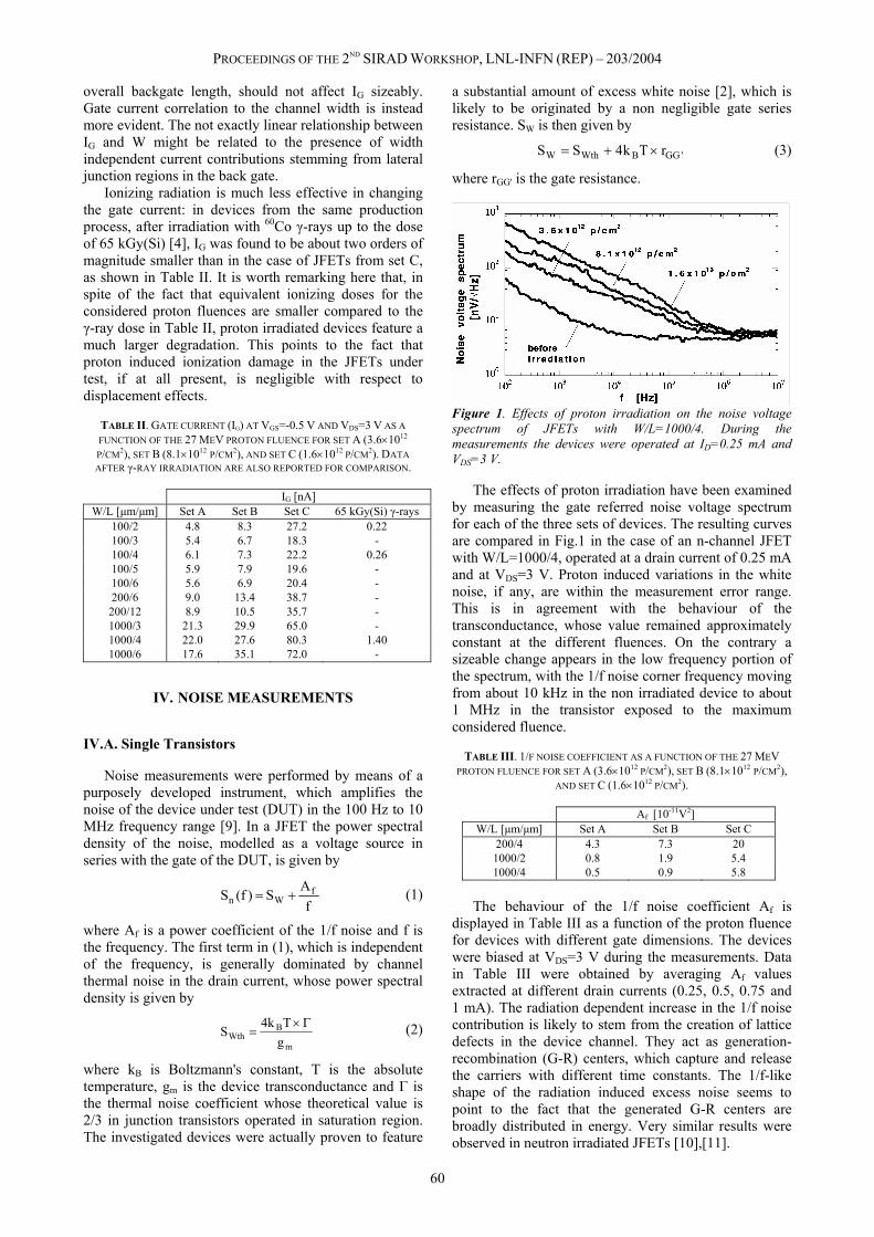
PROCEEDINGS OF THE 2ND SIRAD WORKSHOP, LNL-INFN (REP) – 203/2004
60
overall backgate length, should not affect IG sizeably. Gate current correlation to the channel width is instead more evident. The not exactly linear relationship between IG and W might be related to the presence of width independent current contributions stemming from lateral junction regions in the back gate.
Ionizing radiation is much less effective in changing the gate current: in devices from the same production process, after irradiation with 60Co γ-rays up to the dose of 65 kGy(Si) [4], IG was found to be about two orders of magnitude smaller than in the case of JFETs from set C, as shown in Table II. It is worth remarking here that, in spite of the fact that equivalent ionizing doses for the considered proton fluences are smaller compared to the γ-ray dose in Table II, proton irradiated devices feature a much larger degradation. This points to the fact that proton induced ionization damage in the JFETs under test, if at all present, is negligible with respect to displacement effects.
TABLE II. GATE CURRENT (IG) AT VGS=-0.5 V AND VDS=3 V AS A FUNCTION OF THE 27 MEV PROTON FLUENCE FOR SET A (3.6×10¹² P/CM2), SET B (8.1×10¹² P/CM2), AND SET C (1.6×10¹² P/CM2). DATA AFTER γ-RAY IRRADIATION ARE ALSO REPORTED FOR COMPARISON.
IG [nA] W/L [µm/µm] Set A Set B Set C 65 kGy(Si) γ-rays
100/2 4.8 8.3 27.2 0.22 100/3 5.4 6.7 18.3 - 100/4 6.1 7.3 22.2 0.26 100/5 5.9 7.9 19.6 - 100/6 5.6 6.9 20.4 - 200/6 9.0 13.4 38.7 - 200/12 8.9 10.5 35.7 - 1000/3 21.3 29.9 65.0 - 1000/4 22.0 27.6 80.3 1.40 1000/6 17.6 35.1 72.0 -
IV. NOISE MEASUREMENTS
IV.A. Single Transistors
Noise measurements were performed by means of a purposely developed instrument, which amplifies the noise of the device under test (DUT) in the 100 Hz to 10 MHz frequency range [9]. In a JFET the power spectral density of the noise, modelled as a voltage source in series with the gate of the DUT, is given by
fAS)f(S f
Wn += (1)
where Af is a power coefficient of the 1/f noise and f is the frequency. The first term in (1), which is independent of the frequency, is generally dominated by channel thermal noise in the drain current, whose power spectral density is given by
m
BWth g
Tk4S
Γ×= (2)
where kB is Boltzmann's constant, T is the absolute temperature, gm is the device transconductance and Γ is the thermal noise coefficient whose theoretical value is 2/3 in junction transistors operated in saturation region. The investigated devices were actually proven to feature
a substantial amount of excess white noise [2], which is likely to be originated by a non negligible gate series resistance. SW is then given by
'GGBWthW rTk4SS ×+= (3)
where rGG' is the gate resistance.
Figure 1. Effects of proton irradiation on the noise voltage spectrum of JFETs with W/L=1000/4. During the measurements the devices were operated at ID=0.25 mA and VDS=3 V.
The effects of proton irradiation have been examined by measuring the gate referred noise voltage spectrum for each of the three sets of devices. The resulting curves are compared in Fig.1 in the case of an n-channel JFET with W/L=1000/4, operated at a drain current of 0.25 mA and at VDS=3 V. Proton induced variations in the white noise, if any, are within the measurement error range. This is in agreement with the behaviour of the transconductance, whose value remained approximately constant at the different fluences. On the contrary a sizeable change appears in the low frequency portion of the spectrum, with the 1/f noise corner frequency moving from about 10 kHz in the non irradiated device to about 1 MHz in the transistor exposed to the maximum considered fluence.
TABLE III. 1/F NOISE COEFFICIENT AS A FUNCTION OF THE 27 MEV PROTON FLUENCE FOR SET A (3.6×10¹² P/CM2), SET B (8.1×10¹² P/CM2),
AND SET C (1.6×10¹² P/CM2).
Af [10-11V2] W/L [µm/µm] Set A Set B Set C
200/4 4.3 7.3 20 1000/2 0.8 1.9 5.4 1000/4 0.5 0.9 5.8
The behaviour of the 1/f noise coefficient Af is
displayed in Table III as a function of the proton fluence for devices with different gate dimensions. The devices were biased at VDS=3 V during the measurements. Data in Table III were obtained by averaging Af values extracted at different drain currents (0.25, 0.5, 0.75 and 1 mA). The radiation dependent increase in the 1/f noise contribution is likely to stem from the creation of lattice defects in the device channel. They act as generation-recombination (G-R) centers, which capture and release the carriers with different time constants. The 1/f-like shape of the radiation induced excess noise seems to point to the fact that the generated G-R centers are broadly distributed in energy. Very similar results were observed in neutron irradiated JFETs [10],[11].

PROCEEDINGS OF THE 2ND SIRAD WORKSHOP, LNL-INFN (REP) – 203/2004
61
Figure 2. Effects of 60Co γ-ray and proton irradiation on the noise voltage spectrum of JFETs with W/L=1000/4. During the measurements the devices were operated at ID=0.25 mA and VDS=3 V.
Exposure to γ-rays [4] has a qualitatively different effect on the noise performances of JFET devices, as can be seen in Fig.2, which compares the noise voltage spectra relevant to a non irradiated transistor, a JFET exposed to a 100 kGy(Si) dose of 60Co γ-rays and a device exposed to a 27 MeV proton fluence of 1.6×10¹³ p/cm2 (the same as in Fig.1, belonging to set C). All of them have W/L=1000/4 and were operated at a drain current of 0.25 mA and at VDS=3 V during measurement. In the transistor exposed to γ-rays (which was biased during irradiation at ID=0.25 mA and VDS=3 V), the appearance of a Lorentzian noise contribution [12] can be detected. This phenomenon is typical of JFETs exposed to ionizing radiation; to some extent, the relevant time constant is independent of the fabrication technology and seems to be related only to the polarity of the device [13]. The different behaviour with respect to proton irradiated devices is supposed to be related to a difference in nature of the radiation induced lattice defects.
IV.B. Charge Preamplifiers
A schematic of the all n-JFET charge preamplifier, irradiated together with set A devices at a proton fluence of 3.6×10¹² p/cm2, is shown in Fig.3. The input device has W/L=1000/4 and is operated at ID≈0.25 mA. In this version of the circuit, only active devices are integrated, while passive components are off the chip.
The response of the preamplifier to proton irradiation can be investigated by evaluating its equivalent noise charge. Measurements were performed by means of an eighth order semi-Gaussian unipolar shaper with peaking time adjustable from 500 ns to 24 µs. The ENC model adopted in the case of a JFET amplifier has the following expression
p3F
BG
22f
p
21W
2 tAR
Tk4qI2CAAt1CASENC ⎟⎟
⎠
⎞⎜⎜⎝
⎛+++⋅= (4)
where C is the capacitance shunting the charge sensitive amplifier (CSA) input (including feedback capacitance CF, input capacitance Cin, detector capacitance CD and package stray capacitance Cs), A1, A2 and A3 are shaping coefficients, q is the elementary charge and tp is the signal peaking time at the shaper output. The first term in
(4) is related to white noise contribution in the series noise voltage spectrum, the second one stems from 1/f noise. The third term is due to shot noise in the gate current of the input element and to thermal noise in the feedback resistor RF. The latter contribution can be neglected if the value of RF is suitably chosen [3].
Figure 3. Charge sensitive amplifier with continuous resistive charge reset. RF, CF, R1 and R2 are external components and can be chosen to optimize the circuit operation.
Based on the results discussed in section III and IV.A, it is reasonable to expect that proton irradiation acts mainly on the second and third terms of (4). In Fig.4 the experimental ENC data relevant to a charge sensitive amplifier exposed to a proton fluence of 3.6×10¹² p/cm2 is compared to the equivalent noise charge measured in a non irradiated preamplifier. An increase in the equivalent noise charge is detectable at long peaking times, where the ENC is affected by proton induced degradation in the 1/f noise and gate current related shot noise. In the tested samples, the capacitance C was about 22 pF. RF=1 GΩ in the non irradiated circuit; in the irradiated preamplifier RF was reduced to 10 MΩ in order to compensate for the change in the gate current of the input element and to keep the operating point unchanged. As a general rule, when designing a JFET charge sensitive amplifier for radiation tolerant applications, the feedback resistance should be chosen small enough to accommodate the gate current expected in the worst case scenario. Alternatively, a suitably biased MOSFET, used in place of RF, can handle several decades of gate current and prevent the amplifier output from saturating after irradiation [14].
Again in Fig. 4, the expected ENC at the largest considered fluence is displayed. This curve was calculated on the basis of the noise parameters extracted from noise voltage and static IG measurements in a single transistor belonging to set C and featuring the same gate dimensions (W/L=1000/4) and the same drain current (ID=0.25 mA) as the input device of the preamplifier. In this case radiation induced increase of the 1/f contribution is so large to affect the ENC even in the short peaking time region.

PROCEEDINGS OF THE 2ND SIRAD WORKSHOP, LNL-INFN (REP) – 203/2004
62
Figure 4. Equivalent noise charge as a function of the peaking time at different values of the proton fluence.
V. CORRELATION BETWEEN 60CO γ-RAY AND PROTON INDUCED DAMAGE
In a previous investigation [4] the effects of 60Co γ-rays on n-JFETs and JFET-based charge sensitive amplifiers were examined. In that study γ-ray irradiation was proven to be responsible for a considerable increase in the gate current (although much smaller than that induced by proton irradiation) and for the appearance of a Lorentzian component in the noise spectrum of the investigated devices. Since JFETs are supposed to be to a large extent immune to ionization damage (they do not use silicon oxide for their intrinsic operation) γ-ray induced displacement effects should be considered in order to account for the observed change in device behaviour. As a matter of fact, Compton electrons produced by incident 60Co γ-rays are able to displace atoms from their site in the lattice. However, for a convenient use of 60Co sources in the study of displacement damage, a correlation has to be found with the damage induced by other particles. In the literature, data are provided for the calculation of the fluence of 1 MeV electrons equivalent to irradiate silicon with a γ-ray dose of 10 kGy(Si). In order to extract such conversion factors, the energy spectrum of the Compton generated electrons and the energy dependence of the electron NIEL have to be taken into account [15].
In the following analysis, the gate current has been chosen as the reference parameter for comparing displacement damage effects by protons and γ-rays. Points displayed in the scatter plot of Fig.5 as a function of the equivalent displacement damage were obtained by normalizing each experimental IG value to the bottom gate junction area of the relevant device and by averaging the resulting data of all the irradiated transistors for every single proton fluence and γ-ray dose. In Fig.5, the displacement damage dose was calculated as the fluence multiplied by the Non-Ionizing Energy Loss (NIEL=7.34×10⁻⁶ MeV×cm2/mg for 27 MeV protons, NIEL=0.0314×10⁻⁶ MeV×cm2/mg for 1 MeV electrons). IG,n appears to be dependent only on the displacement damage dose and to be, to a large extent, independent of the radiation type, as one should expect based on the assumption that damage effects are proportional to the displacement damage dose [7],[15]. The result may be interpreted to confirm that, as far as the gate current is
concerned, displacement damage is predominant over ionization effects also in γ-ray irradiated JFETs.
Figure 5. Normalized gate current as a function of the displacement damage dose for proton and γ-ray irradiated n-channel JFETs.
VI. CONCLUSIONS
Sensitivity to 27 MeV protons of n-JFETs and charge preamplifiers fabricated in a detector-compatible process has been investigated. In the irradiated transistors, proton induced displacement damage resulted in a considerable degradation of the gate current and of the 1/f portion of the gate referred noise voltage spectrum. For what concerns the tested charge preamplifiers, after exposure to a proton fluence of 3.6×10¹² p/cm2, a sizeable increase in the equivalent noise charge was detected at peaking times longer than 1 µs. Such a behaviour is likely to be determined by proton induced gate current and 1/f noise increase in the preamplifier input device. Finally the gate current increase, detected in JFETs exposed to 60Co γ-rays, was correlated to proton induced displacement damage. The good linearity of the normalized gate current as a function of the displacement damage dose is the evidence that the tests performed on ITC-irst transistors using different kinds of radiation are accurate and consistent with each other. ____________________ [1] M. Manghisoni et al., "Hard X-ray and gamma-ray detector physics
III", Ralph B. James Editor, Proceedings of SPIE, 4507 (2001) 141. [2] M. Manghisoni et al., IEEE Trans. Nucl. Sci., 50 (2003) 942. [3] G.-F. Dalla Betta et al., Nucl. Instr. Meth., A512 (2003) 199. [4] G.-F. Dalla Betta et al., IEEE Trans. Nucl. Sci., 50 (2003) 2474. [5] J. Wyss et al., Nucl. Instr. Meth., A462 (2001) 426. [6] R. Wunstorf, IEEE Trans. Nucl. Sci., 44 (1997) 806. [7] D. Bisello et al., IEEE Trans. Nucl. Sci., 48 (2001) 1020. [8] A. Candelori et al., IEEE Trans. Nucl. Sci., 50 (2003) 1121. [9] V. Re et al., Nuclear Physics B (Proc. Suppl.), 44 (1990) 599. [10] G. Cesura et al., IEEE Trans. Nucl. Sci., 41 (1994) 577. [11] M. Citterio et al., IEEE Trans. Nucl. Sci., 43 (1996) 1576. [12] K. Kandiah, IEEE Trans. Elect. Dev., 41 (1994) 2006. [13] M. Manghisoni et al., IEEE Trans. Nucl. Sci., 48 (2001) 1598. [14] G. De Geronimo et al., IEEE Trans. Nucl. Sci., 47 (2000) 1458. [15] G. P. Summers et al., IEEE Trans. Nucl. Sci., 40 (1993) 1372.

PROCEEDINGS OF THE 2ND SIRAD WORKSHOP, LNL-INFN (REP) – 203/2004
63
Single Event Upset measurements on the SVX4 chip
N. Bacchetta, D. Pantano, Z. Wang
INFN Sezione di Padova and Dipartimento di Fisica, Università di Padova, Via Marzolo 8, Padova, I-35131, Italy
I. INTRODUCTION
This paper describes the results of Single Event Upset (SEU) measurements on the SVX4 chip [1],[2], developed for the RunIIb upgrade of the silicon detectors for CDF and D0 experiments [3],[4] at the FNAL Tevatron accelerator (Batavia, USA).
The irradiation tests were performed at the SIRAD irradiation facility [5] of the Tandem-XTU accelerator at the INFN National Laboratory of Legnaro (Padova, Italy). We have reported in Table I the energy and the Linear Energy Transfer (LET) of the ions used in the experiment. The beam flux during irradiation was ≈5×10⁴ ions/(cm2×s).
The SVX4 chip was mounted on the standard chip carrier board [6] and was kept under vacuum in the SIRAD experimental chamber. It was readout using the PTS/PTA DAQ system [7] using version 14 of the firmware developed for the CDF RunIIb silicon upgrade project by the University of Illinois at Urbana-Champaign (UIUC) Group in collaboration with the FNAL ESE Department.
TABLE I. ION SPECIES, ENERGY AND CORRESPONDING LINEAR ENERGY TRANSFER (LET) VALUES.
Ion species Energy (MeV) LET (MeV×cm2/mg) Si 163.2 8.4 Cl 175.3 12.5 Va 203.2 22.4 Ni 239.4 28.8
Ag 271.9 58.5 I 286.5 65.7
Two distinct experiments were conducted, the first
aiming to measure the SEU sensitivity of the initialization shift registers, and the second to measure the sensitivity of other parts of the chip by looking at the output data stream. For this reason two C++ programs were written for reading out the SVX4 chip during the tests and to proceed to a quick first level analysis.
The first program downloads the initialization bit-stream in the shift register of the chip and, after a programmable amount of time, reads the output from a priority-out pin and compares it with the original, saving all differences found. The bit-stream is then reloaded and the process is repeated. The time between writing and reading was set for this first test to 2 seconds. The operation of writing/reading takes a few ms.
The second program reads the chip in read-all mode after a trigger accept signal. In read-all mode the chip outputs data on a single 8-bit bus in the following order: Chip ID, PipeCell ID, Channel ID and ADC value for
each of the 128 channels of the chip [3]. With the downloaded parameters we have a typical chip pedestal of about 21 ADC counts, noise around 1.0 ADC count and negligible common mode noise. Every unexpected output value is detected and saved at the end of each readout cycle. When readout data contain evidence of corruption in the initialization bit-stream, the program automatically resets the chip and proceeds to re-initialize it. With this program we can identify: 1) chip ID errors; 2) channel ID errors; 3) anomalies in the pedestal value on a channel by channel basis, i.e. output lower/higher than a specified value, typically either 15 or 30 ADC well separated from noise fluctuations.
Due to the limited time available for irradiation (≈29 hours), we used a rather intense particle flux limiting the time between readout sequences to 1.6 ms. From various known factors at the SIRAD beam line, we estimated the fluence inaccuracy to be below 10%.
II. SEU SENSIBLE PARTS OF THE SVX4 CHIP
There are a limited number of parts of the SVX4 chip sensible to SEU, which can be investigated by our experiment, as shown in Fig.1. These are the initialization shift register with 192 bits, the shadow register where the 64 higher order bits of the shift register are copied, and the output FIFO where output data are stored for readout.
The initialization shift register is the easiest part to be studied as data can be easily stored and read back using specialized input/output pads. However, only the first 128 bits (channel mask bits) of the register can be filled with arbitrary numbers as the remaining bits may affect the proper operation of the chip. Hence, results for this test are based on counting SEUs for the first 128 bits.
The shadow register holds a copy of the higher order 64 bits of the initialization shift register and is implemented by using SEU tolerant techniques. The susceptibility of this part of the chip can be evaluated by counting SEUs in the Chip ID part of the output data. There is no other practical way to check this register as it is very difficult to predict what effect the other bits may have on the output data.
Finally, as data are stored in the output FIFO for serial readout, we can also calculate the susceptibility of this part to SEU by checking Channel ID values in read-all mode. Errors on the digitally converted pedestal values are more difficult to be interpreted as they might be the result of: 1) one or more flipped bits in the shadow register (multiple pedestal errors); 2) real charge deposited by the impinging ion in the analogue storage cells (likely leading to single channel pedestal error).

PROCEEDINGS OF THE 2ND SIRAD WORKSHOP, LNL-INFN (REP) – 203/2004
64
We expect to find a SEU cross section for the output FIFO to be similar to that of the initialization shift register, both much higher than the shadow register.
Figure 1. SEU sensible parts of the SVX4 chip.
III. EXPERIMENTAL RESULTS
The two experiments (initialization bit-stream error counting and normal data taking output error counting) were run separately. During the first experiment the initialization FIFO was open to SEUs for 2 s for each initialization/readout sequence, while time between readouts was limited to 1.6 ms during the second test (the chip was re-initialized at times depending on the error, as previously described).
The offline analysis of the collected data shows various types of errors, which we classified as follows. A) Mismatch in the initialization bit-stream:
A.1. single error on the Mask-Register; A.2. multiple errors affecting the entire initialization register, which are very probably due to SEU induced spurious clocks.
B) Single errors in the chip output data set: B.1. single error of the chip ID; B.2. pedestal value in error for a single channel; B.3. single error of the channel ID.
C) Multiple errors in the chip output data set: C.1. pedestal value for all channels saturates to 255 ADC counts; C.2. pedestal value for all channels goes to a value between 155 and 170 ADC counts; C.3. pedestal value for all channels goes to a common value (0, 9, 55 or 99); C.4. all channel IDs go to 0. C.5. all channel IDs are shifted by the same value.
III.A. Initialization of the Bit-stream
For the first experiment we must distinguish between single bit SEU induced errors (A.1) and what we interpret as SEU induced spurious clocks (A.2) which, by shifting the entire content of the FIFO register, leads to multiple errors in the initialization bit-stream.
The initialization bit-stream is loaded with 64 consecutive "1" followed by 64 consecutive "0" (covering the 128 bits of the channel mask part of the register), while the remaining bits are loaded with a more complicated pattern of "0" and "1", as their meaning directly affects the functionality of the chip. Fig.2 shows the raw error rate for each of the 192 bits as counted during one experiment (200 writing/reading) with 286.5 MeV I ions with LET=65.7 MeV×cm2/mg. We notice that: 1) the 1→0 transition rate is much more probable than
0→1; 2) there is a strong error rate increase at the register
location loaded with the last "0" or with the last "1" of a sequence.
Distribution SEU error versus bitstream
0
20
40
60
80
100
120
140
160
180
1 7 13 19 25 31 37 43 49 55 61 67 73 79 85 91 97 103 109 115 121 127 133 139 145 151 157 163 169 175 181 187
N° of bit
Num
ber o
f SEU
Figure 2. Initialization register error counts for each of the 192 bits. The first 128 bits are the channel mask bits (64 ″1″ for bits 1-64 and 64 ″0″ for bits 65-128).
Figure 3. Normalized error counts of spurious clocks based on data from bits 64, 63, 62 and 61 of the initialization register of Fig.1: data (blue open circles) and Poisson fit (red close diamonds).
The asymmetry 1→0 / 0→1 in the SEU cross section has already been observed for this technology and is in part explained by the difference in the critical charge [9].
The second effect can be easily seen as a dramatic increase of 1→0 and in equal amount 0→1 transitions at the edge of the "1" and "0" filled registers. This can be explained by assuming the occurrence of one or more spurious clocks during the test. Since the first 64 bits are filled with "1" we can interpret the excess errors on bit 63 as a consequence of the occurrence in any given
PROCEEDINGS OF THE 2ND SIRAD WORKSHOP, LNL-INFN (REP) – 203/2004
65
experiment of 1 spurious clock + 2 spurious clocks, and so on. This assumption is confirmed by observing a "rigid" shift of the data content in the shift register by one or more clocks and by fitting the probability distribution of having this type of occurrence (no spurious clocks, 1 spurious clock, 2 spurious clocks, and so on) with a Poisson function, as shown in Fig.3.
Table II and Fig.4 summarize the SEU cross section for the initialization shift register based on the results from the first 128 mask bits. The reported cross section values are total, i.e. for the whole shift register.
TABLE II. SEU CROSS SECTION FOR THE INITIALIZATION SHIFT REGISTER. THIS IS THE TOTAL CROSS SECTION FOR THE WHOLE 192-BIT
SHIFT REGISTER.
Cross section (µm2)
Ion LET (MeV×cm2/mg) 1→0 0→1 Any spurious
clock
Si 8.4 0 0 0
Cl 12.54 0 0 0
Va 22.4 153.6 32.6 7.98
Ni 28.8 3033.6 844.8 366.4
Ag 58.5 ⎯ 1017.6 ⎯
I 65.7 3532.8 806.4 316.6
Figure 4. Total SEU cross section for the whole 192-bit initialization shift register: cross section for 1→0 transitions (blue close circles), 0→1 transitions (green open circles) and for the occurrence of any spurious clock (red solid squares). The Weibull fits (lines) are also shown.
III.B. SEU Sensitivity in Read-all Mode
We can measure the SEU sensitivity of the shadow register from chip ID errors (B.1) and of the readout FIFO from the channel ID errors (B.3). Results on single bit cross sections are reported in Table III. The data in the second and third columns are the measured cross sections for exceeding 15 ADC counts of deposited charge (≈1 fC) and 30 ADC counts (≈2 fC) in a single cell flagged for readout, respectively.
We also observed single channels with a different pedestal value, which we interpreted as real charge
deposited on the pipe cell (B.2). We do not consider the latter to be a SEU, however for completeness we can calculate the cross section of such an occurrence by subtracting from the total the known output FIFO cross section, properly scaled by the number of flipped bits necessary to exceed the threshold of 15 or 30 ADC counts.
As expected the shadow register, being implemented using DICE cells [10], has a higher LET threshold than the regular FIFO registers. Moreover, as expected, the output FIFO has the same threshold and a similar saturation value with respect to the initialization shift register.
Fig.5 shows the total cross section for single bit errors on the initialization shift register, on the shadow register and on the output FIFO. The cross sections for the initialization shift register and output FIFO register are similar while the shadow register has a much higher LET threshold and (very likely) a lower saturation value. Higher LET ions would be necessary for a correct measurement on the shadow register.
TABLE III. MEASURED CROSS SECTION FOR THE SHADOW REGISTER (BASED ON CHIP ID DATA) AND OUTPUT FIFO (BASED ON CHANNEL ID
DATA).
Single Error Cross Section (µm2) Shadow Register
(Chip ID) Output FIFO (Channel ID) Ion
Pipe Cell (non SEU) >1 fC
Pipe Cell (non SEU) >2 fC
1→0 0→1 1→0 0→1
Si ⎯ 15 0 0 0 0 Cl 190 ⎯ 0 0 0 0 Va 183 39 0 0 4.7 1.0 Ni 729 144 0 0 22.9 2.8 Ag ⎯ 260 0.08 0 31.4 4.7 I 793 212 0.34 0 35.5 5.3
Figure 5. Single bit SEU cross section on the initialization shift register, on the shadow register and on the output FIFO. Data are for 1→0 (solid symbols) and 1→0 (open symbols) transitions of the initialization shift register (blue circles), output FIFO (red squares) and shadow register (green triangles). The Weibull fits (lines) are also shown.

PROCEEDINGS OF THE 2ND SIRAD WORKSHOP, LNL-INFN (REP) – 203/2004
66
For multiple errors the situation is more difficult to be interpreted as we observed pedestals moving together to a common value, or saturating, or moving inside a specific range of ADC counts, due in part to flipped bits in the shadow register. Similar situations were observed for the Channel IDs where all channels are shifted by a common value or they all go to zero. We grouped in Table IV the results of the cross section by combining the various types of simply and multiple errors on Pedestals and Channel ID.
Finally, it is quite interesting to compare our measurements with data taken by the CMS Tracker Group on the APV25 read-out chip. The comparison is performed between cross sections on the I2C registers of the APV25 chip (manufactured in IBM 0.25 µm CMOS technology) and the initialization shift register of the SVX4 chip (manufactured in TSMC 0.25 µm CMOS technology) for SEU induced 1→0 transitions. The APV25 data are from [9] and the SVX4 data have been scaled to match the 109 cells of the APV25 I2C register. It is noticeable the agreement for the cross section saturation values and the slightly higher LET threshold of the TSMC process.
TABLE IV. MEASURED MULTIPLE ERROR CROSS SECTION ON PEDESTAL AND CHANNEL ID. THE VALUES COMBINE VARIOUS TYPE OF MULTIPLE ERRORS (C.1, C.2, C.3 FOR PEDESTAL AND C4, C5 FOR CHANNEL ID).
Multiple Error Cross Section (µm2) Ion
Pedestal Channel ID Si 0 0 Cl 0 0 Va 10.24 1.68 Ni 42.75 5.04 Ag 79.11 8.99 I 96.08 11.13
Figure 6. SEU cross section for the 1→0 transitions in the initialisation shift register of the SVX4 chip (blue solid circles) compared to the I2C register of the APV25 chip (red open squares). The Weibull fits (lines) are also shown.
IV. CONCLUSIONS
Our measurements confirm the expected SEU cross section threshold and saturation values for the 0.25 µm CMOS technology. This study also evidences the extreme tolerance to SEU of the DICE cell design.
Nevertheless, we found an unexpected SEU sensitivity, which we interpreted as spurious clocks in the initialization shift register. However all these phenomena have a threshold exceeding the Si maximum LET of 14 MeV×cm2/mg [11],[12] hence the SVX4 chip is perfectly suitable for applications in High Energy Physics colliders. ____________________ [1] M.Garcia-Sciveres et al., Nucl. Instr. Meth., A511 (2003) 171. [2] B.Krieger et al., IEEE Trans. Nucl. Sci., 51 (2004) 1968. [3] M.Aoki et al., Nucl. Instr. Meth., A518 (2004) 270. [4] A.Numerotski et al., Nucl. Instr. Meth., A518 (2004) 295. [5] J. Wyss et al., Nucl. Instr. Meth., A462 (2001) 426. [6] On line available: http://www-cdf.lbl.gov/users/mweber/svx4/ [7] On line available: http://www.hep.uiuc.edu/home/trj/pts/index.html [8] L. Christofeck et al., "SVX4 user’s manual", D0-NOTE,
5 September 2003. [9] E. Noah et al., Nucl. Instr. Meth., A492 (2002) 434. [10] T. Calin et al., IEEE Tran. Nucl. Sci., 43 (1996) 2874. [11] P. M. O’Neill et al., IEEE Trans. Nucl. Sci., 45 (1998) 2467. [12] J. H. Adams Jr., "Cosmic ray effects on microelectronics, Part IV",
Naval Research Laboratory Memorandum Report 5901, 31 December 1986.

PROCEEDINGS OF THE 2ND SIRAD WORKSHOP, LNL-INFN (REP) – 203/2004
67
Heavy ion irradiation of the XAA1.2 ASIC chip for space applications
E. Del Monte1,2, L. Pacciani1, G. Porrovecchio1, P. Soffitta1, E. Costa1, G. Di Persio1, M. Feroci1, M. Mastropietro3, E. Morelli4, M. Rapisarda5, A. Rubini1, D. Bisello6, A. Candelori6, A. Kaminski6, J. Wyss7
1IASF-CNR, Via Fosso del Cavaliere 100, Roma, I-00133, Italy
2Dipartimento di Fisica, Università di Roma "Tor Vergata", Via della Ricerca Scientifica 1, Roma, I-00133, Italy
3IMIP-CNR, Via Salaria km 29.300, Monterotondo Scalo (Roma), c.p. 10, I-00016, Italy
4IASF-CNR, Via P. Gobetti 101, Bologna, I-40129, Italy
5ENEA, Centro di Ricerca di Frascati, Via Enrico Fermi 45, Frascati (Roma), I-00044, Italy
6INFN Sezione di Padova and Dipartimento di Fisica, Università di Padova, Via Marzolo 8, Padova, I-35131, Italy
7D.I.M.S.A.T., Università di Cassino, Via Di Biasio 43, Cassino (Frosinone), I-03043, Italy
I. INTRODUCTION
Application Specific Integrated Circuits (ASICs) are widely used as front-end electronic chips in satellite borne experiments because of their good performances together with small dimensions and low power consumption. A serious disadvantage is that the complementary metal oxide semiconductor (CMOS) technology, on which most of the ASIC design is based, is particularly sensitive to radiation effects induced by cosmic rays (see for example [1],[2]).
These radiation-induced effects are generally investigated by irradiating the devices with protons or ions in an accelerator dedicated facility. In these tests incident particles with different atomic number and energy are selected, thus obtaining different Linear Energy Transfer (LET) values in the chip sensitive region.
The topic of this study is to investigate the effects induced by radiation (i.e., latch-up, Single Event Upset (SEU) and Total Ionizing Dose (TID)) on the XAA1.2 ASIC chip by heavy ion irradiation. The XAA1.2 chip has been selected as the front-end electronic circuit of the SuperAGILE experiment on board the AGILE satellite mission.
II. OVERVIEW OF THE XAA1.2 CHIP
The XAA1.2 chip is a very large scale integration (VLSI) ASIC designed by Ideas ASA (Oslo, Norway) as a front-end electronic circuit for silicon microstrip detectors. The chip is manufactured by using a 0.8 µm CMOS double-poly and double-metal technology on epitaxial layer. This chip is not specifically designed as a radiation hard component for space applications: it is a custom ASIC designed starting from the Ideas ASA commercial device XA1.3 after making design modifications aiming to improve the performance in term of noise, power consumption and thermal stability by means of an extensive laboratory testing, as reported in [3].
The XAA1.2 chip has a 6×8 mm2 surface and a 600 µm thickness. It is divided in 128 data driven and self-triggering input channels, consisting of an analog and a digital part, and it is designed to detect single hit events with sparse readout. The main features of this chip as a front-end electronic circuit for silicon microstrip detectors are described in [4].
Each analogue signal processing chain is composed of a charge sensitive preamplifier, a CR-RC shaper and a peak store unit, which contains a peak stretcher, as shown in Fig.1. The peak stretcher can be excluded and bypassed by changing the digital configuration of the ASIC, thus reducing the overall power consumption.
The digital section can be programmed with a 646 bit long register, built inside the chip and serially loaded. This register contains a 646 bit-stream, referred to as configuration mask, encoding all the information needed to configure the chip.
Figure 1. Schematic of the XAA1.2 analog channel. From left: the preamplifier, the shaper, the peak stretcher and the discriminator.
The XAA1.2 chip is biased by using four voltages, two for the analogue section (AVDD=+2.0 V and AVSS=-2.0 V) and two for the digital section (DVDD=+2.0 V and DVSS=-2.0 V). Since the power consumption of the digital part is negligible, we can take the analogue voltages and currents as the chip bias voltages (VDD=+2.0 V and VSS=-2.0 V) and currents (IDD and ISS).

PROCEEDINGS OF THE 2ND SIRAD WORKSHOP, LNL-INFN (REP) – 203/2004
68
III. EXPERIMENTAL SETUP
In order to study the XAA1.2 sensitivity to latch-up, SEU and TID, heavy ion irradiations were performed at the SIRAD irradiation facility [5] of the Tandem-XTU accelerator at the INFN National Laboratory of Legnaro (Padova, Italy).
We have irradiated three XAA1.2 chips, each one mounted on its test printed circuit board (PCB), with serial number 710-1-3, 710-1-12 and 710-1-25, respectively. Hereafter each chip is identified with the serial number of its board. Each board contains only one XAA1.2 device, which is the only active element. The boards are covered by an Al layer ≈1 mm thick with a rectangular window placed above the chip. In this way we prevent the incident ions from reaching the other components of the PCB different from the chip.
The measurements were performed using the XA-DAQ board, manufactured by Ideas ASA to supply and configure the circuit and to measure its linearity and threshold by an internal pulse generator.
In Table I we show the ion species used to irradiate each XAA1.2 chip together with the values of energy, LET and range in silicon. The LET data have been determined by SRIM [6] for a silicon target.
TABLE I. ION SPECIES USED DURING THE IRRADIATION WITH ENERGY, LET IN SILICON AND SERIAL NUMBER OF THE IRRADIATED CHIP.
Ion species Energy (MeV)
LET (MeV×cm2/mg)
Irradiated chip
16O 108.7 2.9 710-1-25 16O 58.2 4.2 710-1-12 28Si 157.7 8.6 710-1-12, 710-1-25 32S 171.7 11.0 710-1-3, 710-1-25
48Ti 196.2 19.8 710-1-3, 710-1-12, 710-1-25
58Ni 220.7 28.4 710-1-3, 710-1-12, 710-1-25
79Br 255.7 38.5 710-1-12 107Ag 273.8 54.7 710-1-12
127I 276.7 61.8 710-1-12, 710-1-25 197Au 275.7 81.7 710-1-12
IV. LATCH-UP MEASUREMENTS
The latch-up is a sudden increase of the chip bias currents as a consequence of a particle impact. The latch-up is dangerous because the high current flow produces an overheating that can damage the chip or other elements such as the wire bondings. Moreover after it is triggered, the high current state is steady and can last for tens of seconds.
In order to study the latch-up occurrence, we monitored the power supply currents IDD and ISS by the XA-DAQ board during irradiation. A threshold is set for each current and the number of times one of the two currents exceeds its threshold is recorded and considered as a latch-up event. The current increase due to a latch-up is faster than the 0.3 s sampling time of the current monitor and this fact does not allow to study the temporal evolution of the variation for the supply currents.
From the irradiation results we can calculate the probability and the cross section of the latch-up occurrence as a function of LET. If Nlatch-up is the number of latch-up events for a fixed LET, ϕ is the ion flux, t is the irradiation time and S is the chip geometric surface (0.48 cm2), the latch-up probability is
Platch-up=Nlatch-up/(ϕ⋅t⋅S) (1)
and the cross section is given by
σlatch-up=Nlatch-up/(ϕ⋅t)=Platch-up⋅ S (2)
The latch-up probability and cross section for the three chips under test are plotted in Fig.2 as a function of LET. If LET≥LETthr the latch-up cross section σlatch-up can be fitted as a function of LET by a Weibull function
σlatch-up=σ∞(1-exp-[(LET-LETthr)/W]S) (3)
where σ∞ is the saturation or plateau cross section, LETthr is the LET threshold, i.e. the maximum LET value that has a zero cross section, W and S are dimensionless shape parameters (see [7] for more information). In this definition σlatch-up=0 if LET<LETthr. Applying the Weibull function to the latch-up data of the chip 710-1-12 we find that σ∞=(1.7±0.1)×10-3 cm2, LETthr=(8.5±3.6) MeV×cm2/mg, W=(3.9±0.3)×10-2 and S=(5.4±2.7). With the same function the fitting parameters for the chip 710-1-25 are σ∞=(2.2±0.2)×10-3 cm2, LETthr=(4.2±1.7) MeV×cm2/mg, W=(4.0±0.2)×10-2 and S=(9.5±1.5).
Figure 2. Latch-up cross section (σlatch-up) and probability (Platch-up) as a function of LET for the three chips under test.
V. SEU MEASUREMENTS
The SEU is a bit flip in the digital part of a circuit as a consequence of a particle impact. This effect is dangerous because the circuit configuration can change and an unpredictable functionality can result.
We study the SEU occurrence comparing the input configuration bit-stream with the mask recorded in the chip memory registers. In case of a SEU, one or more bit in the memory registers change their polarity state. The number of SEU events is recorded in the approximation that an ion interaction can change only a single bit of the configuration mask at a time.

PROCEEDINGS OF THE 2ND SIRAD WORKSHOP, LNL-INFN (REP) – 203/2004
69
As for the latch-up, we calculate the SEU probability (PSEU) and cross section (σSEU) as a function of the different LET values. If NSEU is the number of SEU events for a fixed LET value, ϕ is the ion flux, t is the irradiation time and S is the chip geometric surface, the probability is
PSEU=NSEU/(ϕ⋅t⋅S) (4)
and the cross section is given by
σSEU=NSEU/(ϕ⋅t)=PSEU⋅S (5)
The SEU probability and cross section for the three chips under test are plotted in Fig.3 as a function of LET. The LET threshold for the SEU events can be defined as the maximum LET value that has a zero cross section. Since for the chip 710-1-12 we record an event at the smallest LET value (4.15 MeV×cm2/mg for 16O), we calculate the threshold basing only on the results of this chip. Using a linear extrapolation we find that the threshold is LETthr=3.9±0.3 MeV×cm2/mg.
Figure 3. SEU cross section (σSEU) and probability (PSEU) as a function of LET for the three chips under test.
VI. TID EFFECTS
TID effects are due to charge trapping in the oxides of microelectronic devices as a consequence of the energy deposited by ionizing radiation.
The variation of the performance of the XAA1.2 chips have been measured during irradiation as a function of the surface dose (d), which can be calculated, if expressed in krad(Si), by
d=LET⋅ϕ⋅t/(6.24⋅107) (6)
where the LET is measured in MeV×cm2/mg, ϕ is the ion flux, t is the irradiation time and 6.24⋅107 is a numerical conversion factor between the energy units.
During the irradiation we monitored the bias voltages (VSS and VDD) and the power supply currents (ISS and IDD) of the XAA1.2 chip, in order to calculate the power consumption for each input channel as
P=[ISS⋅VSS+IDD⋅VDD]/128 (7)
The power consumption of the three XAA1.2 chips as a function of the dose is shown in Fig.4. The supply voltages VSS and VDD were stable during irradiation. The
power consumption of the chips 710-1-3 and 710-1-25 increases as a function of the dose, while the power consumption of the chip 710-1-12 decreases between 1 krad(Si) and 17 krad(Si) and then begins to increase. The amount of power consumption variations depends on the particular considered chip.
The maximum expected dose absorbed by the chip on-orbit as part of the SuperAGILE front-end electronics is 3 krad(Si). From a linear interpolation of the measured values, we find that the power consumption at 3 krad(Si) is 0.47 mW/channel for the chip 710-1-3 (-2% variation), 0.54 mW/channel for the chip 710-1-12 (no variation) and 0.60 mW/channel for the chip 710-1-25 (+2% variation).
Figure 4. Power consumption as a function of dose for the three chips under test.
Figure 5. Amplitude of the output signal from the chip 710-1-25 as a function of the input charge for different dose values.
As a measure of the chip performance as a function of the dose, we can consider the linearity curve of the chip 710-1-25, obtained by the internal test pulse generator. Taking into account that 3.62 eV are required to generate one electron-hole pair in silicon, the chip linearity was tested from 0.41 fC (corresponding to 10 keV) up to 5.64 fC (corresponding to 128 keV). As shown in Fig.5, the linearity of the XAA1.2 chip does not show significant variations at a dose level of 1 krad(Si), some linearity variations can be seen at a 173 krad(Si) level, i.e. orders of magnitude above the maximum expected dose, while the chip is not linear at 675 krad(Si).

PROCEEDINGS OF THE 2ND SIRAD WORKSHOP, LNL-INFN (REP) – 203/2004
70
VII. CONCLUSIONS
Ion irradiation tests were performed at the SIRAD facility of the 15 MV Tandem-XTU accelerator at the INFN National Laboratory of Legnaro, in order to study the radiation induced effects on the XAA1.2 chip. This read-out electronic device, which is manufactured by a 0.8 µm CMOS technology on epitaxial layer, was not originally developed as a radiation resistant component for space applications.
Latch-up and SEU are the two main Single Event Effects caused by the space radiation environment on electronic circuits. The latch-up and SEU probability and cross section have been evaluated by heavy ion irradiation, particularly the mean LET threshold is (5.0±1.5) MeV×cm2/mg for latch-up and (3.9±0.3) MeV×cm2/mg for SEU.
TID effects on the linearity and power consumption of the XAA1.2 chip have been also investigated. The chip power consumption increases significantly above ≈100 krad(Si) and the chip is linear up to a dose of ≈173 krad(Si). Nevertheless, the performance variations due to TID effects are negligible for the XAA1.2 chips in the SuperAGILE application, where the maximum expected dose on-orbit is 3 krad(Si). ____________________ [1] T. Goka et al., IEEE Trans. Nucl. Sci., 38 (1991) 1693. [2] L. Adams et al., IEEE Trans. Nucl. Sci., 39 (1992) 1804. [3] E. Del Monte et al., Proceedings of SPIE, 4140 (2002) 584. [4] P. Soffitta et al., Proceedings of SPIE, 4140 (2002) 283. [5] J. Wyss et al., Nucl. Instr. Meth., A462 (2001) 426. [6] J. F. Zigler, "SRIM-2000, Stopping and range of ions in matter",
IBM-Reasearch, Yorktown, NY, 10598, USA. On line available: http://www.research.ibm.com/ionbeams/.
[7] E. L. Petersen et al., IEEE Trans. Nucl. Sci., 39 (1992) 1577.

PROCEEDINGS OF THE 2ND SIRAD WORKSHOP, LNL-INFN (REP) – 203/2004
71
Radiation testing of the GLAST LAT tracker ASICs
R. Rando1, A. Bangert2, D. Bisello1, A. Candelori1, P. Giubilato1, M. Hirayama2, R. Johnson2, H. F.-W. Sadrozinski2, M. Sugizaki2, J. Wyss3, M. Ziegler2
1INFN Sezione di Padova and Dipartimento di Fisica, Università di Padova, via Marzolo 8, Padova, I-35131, Italy
2SCIPP, University of California at Santa Cruz, 1156 High Street, Santa Cruz, CA, USA
3D.I.M.S.A.T., Università di Cassino, via Di Biasio 43, Cassino (Frosinone), I-03043, Italy
I. INTRODUCTION
Galactic and extragalactic gamma ray sources are of great interest to both High Energy Astrophysics and Particle Physics. The Large Area Telescope (LAT) [1],[2] on the Gamma-ray Large Area Space Telescope (GLAST) is a next generation gamma-ray pair conversion telescope that makes use of a silicon-strip detector tracker (TKR) [3]. The LAT will observe celestial gamma-ray sources in the energy range from 20 MeV to 300 GeV with a field of view greater than 2 steradians.
The tungsten foils preceding the detector planes in the TKR convert the incident gamma-ray photons into electron-positron pairs, which are then tracked by the silicon layers to determine the photon direction. Finally, a CsI calorimeter (CAL) absorbs the secondary particles and thereby measures the primary photon energy. Silicon-strip detector technology provides nearly 100% detection efficiency for charged particles, optimal angular resolution, small dead time, excellent multi-track separation and self triggering capability. Furthermore, it is known to be robust, requires no consumables, and operates at a relatively low voltage, all of which are ideal features for space applications.
The purpose of this work is to report the process of Radiation Hardness Assurance (RHA) for the LAT TKR flight ASICs as performed at the INFN National Laboratory of Legnaro (Padova, Italy).
II. TKR ELECTRONICS
The GLAST LAT detector is highly modular: it consists of 16 tower modules, each of which has an 18 layer TKR, the CsI CAL and the Tower Electronic Module (TEM) readout electronics. Two silicon layers, oriented at 90 degrees with respect to each other, are contained in each TKR tray; the whole tracker has a total silicon surface of about 83 m2, segmented into almost 885000 channels.
Each silicon layer is connected through a pitch adapter to a hybrid Multi-Chip Module (MCM), containing the layer readout ASICs. The readout is implemented using two ASICs, produced in Agilent 0.5 µm CMOS technology. The GLAST LAT Front End (GTFE) ASICs are composed of an analog part (amplifier-shaper-threshold; 64 channels) plus the digital blocks for digitalization and communication [4],[5]. Pulse-size analysis is not needed for GLAST, so power
restrictions naturally lead to a binary readout with a simple single-threshold discriminator for each channel. A fast trigger is generated easily by calculating the logical OR of all GTFE channels in each layer.
Each MCM accommodates 24 GTFE ASICs, each connected to its neighbours to allow data transfer and trigger propagation. A GLAST LAT Readout Controller (GTRC) ASIC, a fully digital chip that interfaces the GTFEs with the data acquisition electronics in the DAQ, lies at both ends of this chain. Taking into account the number of towers, layers and channels in a layer, we obtain a total of 13824 GTFEs and 1152 GTRCs in the whole TKR.
Each GTFE ASIC contains three 64 bit registers that enable-disable calibration pulse, data taking and trigger generation capabilities for each channel (henceforth labelled CAL, CHN and TRG respectively). Another 14 bit register (DAC) sets calibration pulse and cut-off threshold levels, while a small, two bit register (DEAF) permits the selection of leftward and rightward readout and the switching off of a malfunctioning chip.
Each GTRC ASIC has two registers: REG (34 bits) has 22 bits used to store configuration parameters, 7 bits used as error and status flags and 5 bits which enable the modification of specific parts of the configuration, while SYNC (5 bits) controls synchronization with the GTFEs.
III. RADIATION ENVIRONMENT
TKR ASICs will be exposed to ionizing radiation and, consequently, to radiation induced damage, which can be classified into two categories: Single Event Effects (SEE) and Total Ionizing Dose (TID) effects.
Among all SEEs the most relevant for the LAT are Single Event Upset (SEU) and Single Event Latch-up (SEL). In a SEU a single particle releases enough charge in the proximity of a memory cell to change its status (1→0 or 0→1), thus corrupting data or modifying the ASIC configuration. To limit the impact of these phenomena all registers in both GTFE and GTRC ASICs are SEU-hardened [6]. In a SEL the energy released by a single particle is injected into parasitic p-n-p-n structures inherent to CMOS technology, triggering a short-circuit that can lead to the destruction of the affected device.
The Agilent 0.5 µm CMOS process is relatively radiation hard, being based on an epitaxial structure (the thickness of the processed layer is about 13 µm including the epitaxial layer). This technology has already been shown to be SEU resistant to heavy ions [7].

PROCEEDINGS OF THE 2ND SIRAD WORKSHOP, LNL-INFN (REP) – 203/2004
72
GLAST will be in a Low Earth Orbit (LEO), at an altitude of 565 km and an inclination of 28.5 degrees [8]. The instrumentation will be consequently shielded from a large portion of the space radiation. The orbit will, however, intersect the South Atlantic Anomaly (SAA) which will give the most important contribution to total dose.
The radiation environment in which the telescope will operate is well understood [8]. The spectra of Galactic Cosmic Ray (GCR) nuclei are well represented by the CREME model; the Solar Particle Event (SPE) contribution is calculated, taking into account the modulation of solar activity and the corresponding atmospheric influence on the magnetic belts. Albedo from charged particles interacting with the Earth atmosphere is described by data collected during previous experiments.
The expected Total Ionizing Dose is due mainly to trapped protons in the SAA. The accumulated TID in a 5 year mission is about 0.8 krad(Si) in the TKR outer layers. Allowing for a factor five engineering margin, we obtain about 4 krad(Si); we required testing of all ASICs up to 10 krad(Si) to allow for a further safety margin of 12.5 times.
For SEE issues we will consider GCR and SPE, taking into account the Linear Energy Transfer (LET) at the surface of silicon. Irradiation performed on analog-digital test structures containing four 32 bit registers indicates a SEE threshold of about 8 MeV×cm2/mg [9]; since this threshold value is confirmed by the data presented in this report, the threshold will be held fixed to this value when fitting to simplify the convergence. Above this LET we estimate a worst case scenario by multiplying the maximum possible particle flux in the planned 5 years of operation by the total mission time, obtaining ≈0.2 ions/cm2 due to GCR and <0.1 ions/cm2 due to SPE in 5 years. As a conservative upper limit we will then assume a fluence of 1 ion/cm2 in 5 years above the SEE LET threshold (8 MeV×cm2/mg). We require the expected number of upsets in the whole LAT in 5 years to be smaller than about 700. As LAT configuration data will be reloaded periodically, this SEU rate is an acceptable safety factor to avoid an excessive data loss. Expected SELs, far more dangerous, must be less than 0.5 in 5 years.
IV. EXPERIMENTAL PROCEDURE
For the Radiation Hardness Assurance of TKR ASICs, we first investigated several samples to understand their behaviour after irradiation (SEE threshold and saturation, TID effects) [10]; the obtained results are reported in the following sections. The derived test plan was then applied in the validation phase to ASICs coming from the flight lot: 2 GTFEs and 2 GTRCs were required to be tested for SEE effects and 7 ASICs of each type for TID. Results for flight lot parts are perfectly consistent with what is reported here.
All requirements are specified in [10],[11]; for all irradiations we used smaller area test-MCMs which can accommodate only 7 GTFEs and 2 GTRCs. Heavy ion irradiations were performed at the SIRAD beam line of
the INFN National Laboratory of Legnaro [12]. A 15 MV Tandem Van de Graaff accelerator provides ion beams ranging from H to Au. A summary of the ion beams used for this study is reported in Table I. The surface LET values range from the aforementioned lower threshold (8 MeV×cm2/mg) up to about 80 MeV×cm2/mg, well above the value when SEE saturation is expected from previous measurements on test structures [9] (around 35 MeV×cm2/mg).
TABLE I. ION SPECIES AT SIRAD.
Ion species
LET (MeV×cm2/mg)
Range in Si (µm)
28Si 8.5 62 58Ni 28.4 34 79Br 38.8 31
107Ag 54.7 28 197Au 81.7 23
For TID we used gamma rays from the 4π 60Co
source of the CNR-ISOF at the INFN National Laboratory of Legnaro. Following standard ASTM and MIL procedures (see for example [13]), devices were placed within a Pb-Al box (wall thickness: 2.5 mm Al, 2 mm Pb) to eliminate low energy photon and electron components that can lead to dose enhancement on the device under test (DUT) surface. Each DUT was powered and clocked during irradiation; uniformity and dose rate were experimentally verified before the validation phase started and were found to be, as expected, in agreement to geometrical considerations (dose rate 1 rad(Si)/s, uniformity better than 10% on a test-MCM).
Devices were biased during irradiation by a custom-built power supply, designed to detect a SEL in less than 1 µs. A built-in serial interface allowed the user to monitor such events from a PC and log them together with other SEE/TID data.
Tests required for TID RHA are listed in Table II and Table III: functionality tests were selected to cover the basic digital capabilities of each ASIC, while performance tests were focused on the GTFE analog front-end. All tests were repeated before and after irradiation and results obtained were compared; it is assumed here that ASICs reaching the radiation validation phase operate properly (i.e., the relevant parameters are all within acceptable limits before irradiation).
In addition to the tests reported in Tables III and Table IV power consumption was monitored to ensure that an eventual increase has to be smaller than 20%; no increase in power consumption due to radiation damage was observed.
More details, including ASIC configuration during tests and RHA requirements can be found in [11].
V. EXPERIMENTAL RESULTS: SEE
The irradiation was divided in two parts for each ion beam: in the first we wrote in the registers a series of alternating "1" and "0" ("picket fence" pattern), waited for 10 seconds, read back the registers and checked for

PROCEEDINGS OF THE 2ND SIRAD WORKSHOP, LNL-INFN (REP) – 203/2004
73
errors. During the second part the pattern was substituted with its complementary.
The resultant SEU cross sections per bit as obtained in these irradiations are reported in Table IV. The errors in Table IV are inferred from the number of observed events given by Poisson statistics; the error on the delivered fluence is negligible in comparison. GTFE registers with less than 64 bits are ignored in this analysis since they are statistically less significant due to the limited number of bits which they contain (14 and 2 respectively), while SEU tests for GTRC REG are limited to the last 22 bits (labelled CONF bits) as other bits have special functions.
TABLE II. ASIC FUNCTIONALITY TESTS.
Test Short Description GTRC Register
R/W Load bit pattern in GTRC registers, read it back and check for errors.
GTFE Register R/W
Load bit pattern in GTFE registers, read it back and check for errors. Access GTFE individually.
GTFE Register Broadcast R/W
Load bit pattern in GTFE registers, read it back and check for errors. Broadcast commands.
GTRC Addressing GTRC register R/W test, repeat for all possible GTRC layer IDs.
Hard and Soft Reset Load non-default pattern in GTFE registers. Reset and read back pattern. Repeat for soft and hard reset.
TABLE III. GTFE PERFORMANCE TESTS.
Test Short Description Noise Rate Measure noise rate on Layer-OR channel.
No calibration strobe. Readout with
Charge Injection Complete readout sequence, with calibration strobe. Repeat for all GTFE internal buffers. Check event buffer and Layer-OR.
Register Mask Tests Disable all channels. Complete readout sequence, with calibration strobe. Check event buffer and Layer-OR to be empty.
Threshold Test with Charge Injection
Set threshold to complete readout sequence, with calibration strobe. Check event buffer and Layer-OR.
In Table V we report the parameters obtained fitting
the SEU cross sections per ASIC with the Weibull function [14]
⎟⎟⎠
⎞⎜⎜⎝
⎛⎟⎠⎞
⎜⎝⎛ −−−⋅=
WLL
SLSEU0exp1)(σ (1)
where L0 is the LET threshold, L>L0 is the ion LET, S is the saturation limiting value and W is the curve width. Fit curves and experimental data are shown in Fig.1. For σSEU-CONF we had to further constrain the fit to force convergence: we fixed the width W to the weighted average calculated for the GTFE registers. We thus have at least an estimate for the saturation limiting value of σSEU-CONF.
SEL upper limits are reported in Table VI. Notably no latch-ups were observed even after 5×10⁶ Au ions/cm2 on GTRC DUTs and 4×10⁶ Au ions/cm2 on GTFEs.
Expected number and upper limits (where appropriate) of SEU and SEL for the whole tracker for a mission lasting 5 years are shown in Table VII. In the case of SEU, we have calculated the weighted average of
all the S values in Table VI, including the one for σSEU-CONF, obtaining <S>=(1.77±0.16)×10-7 cm2/(ion×bit). Even if σSEU-CONF were excluded from the average we would obtain <S’>=(1.93±0.28)×10-7 cm2/(ion×bit), compatible with the former estimate within 1 σ. To obtain the SEU estimates we multiplied this average saturation limit by the number of ions hitting the TKR in 5 years and by the total number of bits in the considered ASIC; for GTRC we have ignored "special" bits in REG as a SEU occurring there will not change the behaviour of the electronics.
TABLE IV. SEU CROSS SECTIONS [CM2/(ION×BIT)].
LET [MeV×cm2/mg]
σCAL (×10-8)
σTRG
(×10-8) σCHN
(×10-8) 8.5 < 0.1 < 0.1 < 0.1
28.4 10.4±1.4 11.3±1.5 9.8±1.4 38.8 9.6±1.6 12.8±1.8 7.6±1.4 54.7 31.6±3.5 16.4±2.5 17.2±2.6
TABLE V. SEU WEIBULL FIT PARAMETERS.
Register S [cm2/(bit×ion)]
L0 (fixed) [MeV×cm2/mg]
W [MeV×cm2/mg]
σSEU-CAL (3.1±1.1)×10-7 8 57±30 σSEU-TRG (1.8±0.3)×10-7 8 22±8 σSEU-CHN (2.9±1.4)×10-7 8 68±46 σSEU-CONF (1.7±0.2)×10-7 8 25 (fixed)
0 10 20 30 40 50 60 70 80
σCALfit σCALσTRGfit σTRGσCHNfit σCHNσCONFfit σCONF
LET [MeV·cm2/mg)]
σ SE
U[×
10-8
cm2 /(
bit ·
ion)
]
0.1
1.0
10
100
0 10 20 30 40 50 60 70 80
σCALfit σCALσTRGfit σTRGσCHNfit σCHNσCONFfit σCONF
LET [MeV·cm2/mg)]
σ SE
U[×
10-8
cm2 /(
bit ·
ion)
]
0.1
1.0
10
100
Figure 1. Weibull fit of SEU cross sections. In the plot data are shown for the three GTFE 64 bit registers, together with the CONF part of the GTRC REG register (i.e., the last 22 bits).
TABLE VI. SEL CROSS SECTIONS UPPER LIMITS.
ASIC Delivered Au fluence [ions/cm2]
σSEL at 95% confidence level. [×10-7 cm2/(ion×ASIC)]
GTRC 5×10⁶ <6.0 GTFE 4×10⁶ <7.5
TABLE VII. SEE IN A 5 YEAR MISSION, WHOLE TKR.
SEE Expected in GTFE (Upper limit, where < )
Expected in GTRC (Upper limit, where < )
SEU 0.7 0.005 SEL < 0.01 < 0.0007

PROCEEDINGS OF THE 2ND SIRAD WORKSHOP, LNL-INFN (REP) – 203/2004
74
VI. EXPERIMENTAL RESULTS: TID
A subset of the test procedures used for ASIC screening on the wafers was selected to be employed for TID validation with 60Co gamma rays. In [11] a detailed description of the performed tests is given.
Power consumption was monitored to look for an increase due to ionizing radiation; no significant increase after irradiation was observed, while fluctuations remained within 5%.
A series of functionality tests was performed on both GTRC and GTFE ASICs. Monitored functionalities include register access and modification and, for GTFE only, analog performances: noise, gain, threshold and calibration pulse were thoroughly examined (see Table II and Table III). The entire test set was repeated before irradiation and after each 2.5 krad(Si) step up to a total dose of 10 krad(Si). No significant change in DUT behaviour was observed. As an example of TID tests we will present some data about GTFE noise.
Figure 2. Typical noise versus threshold curves for a GTFE, measured before and after 60Co γ-ray irradiation up to the dose of 10 krad(Si) on the OR channel. Arrows indicate the following point is equal to zero.
A measurement of the noise rate as a function of the threshold level before and after irradiation is shown in Fig.2 for a sample GTFE. The noise rate measurement is performed on the OR channel and the chip was not triggered, as the OR operation does not require it. Charge injection (calibration pulse) was not used: the measured noise is intrinsic to the front end. Validation requires the noise rate to be below 100 Hz per chip if the threshold is set to 10 (corresponding to ≈0.5 fC); this constraint was easily met by all GTFEs we tested. Although it appears that noise rate increases at the lowest threshold values (below 5 DAC) due to ionizing radiation, at higher threshold values it actually decreases: this means that the Equivalent Noise Charge (ENC) actually decreases with radiation. At very low thresholds saturation may occur and the threshold offsets or the shaping time might change slightly due to irradiation. A further, dedicated analysis of this behaviour is required in order to understand it.
All other functionality tests gave good results: we did not observe any problem due to radiation damage in all the tested devices.
VII. CONCLUSIONS
We tested LAT TKR ASICs both for SEE and for TID effects. No catastrophic damage was observed in any tested device. The number of expected SEEs in the LAT TKR is negligible for the planned 5 year mission, even considering that over 13000 ASICs will be employed.
GLAST internal documents and technical reports can be accessed through the SLAC GLAST-LAT Document System [15]. ____________________ [1] P. F. Michelson, "GLAST LAT", Response to AO 99-OSS-03,
Stanford University, E 2002. [2] P. F. Michelson, "GLAST: a detector for high-energy gamma
rays", Proceedings of SPIE, 2806 (1996) 31. [3] W. B. Atwood et al., Nucl. Instr. Meth., A435 (1999) 224. [4] R. P. Johnson et al., IEEE Trans. Nucl. Sci., 45 (1998) 927. [5] R.P. Johnson et al., "The readout electronics for silicon tracker of
the GLAST beam test engineering model", presented at the 4th International Symposium on Development and Application of Semiconductor Tracking Detectors, Hiroshima, Japan, March 2000.
[6] L. R. Rockett, IEEE Trans. Nucl. Sci., 35 (1998) 1682. [7] J. V. Osborn et al., "Single event latch-up characteristics of three
commercial CMOS processes", Proceedings of the 7th NASA Symposium on VLSI Design, 1998.
[8] "GLAST mission system specification", 433-SPEC-001, GSFC, October 2002.
[9] M. Sugizaki et al., "SEE test of the LAT tracker front end ASIC", SLAC, Menlo Park, CA, Tech. Rep., LAT-TD-00333, 2001.
[10] R. Rando et al., "Radiation tests of GLAST LAT electronic components at LNL", SLAC, Menlo Park, CA, Tech. Rep., LAT-PS-01059, 2002.
[11] R. Rando et al., "Radiation test plan for the GLAST LAT TKR ASICs", SLAC, Menlo Park, CA, Tech. Rep., LAT-PS-01325, 2003.
[12] J. Wyss et al., Nucl. Instr. Meth., A462 (2001) 426. [13] "Standard guide for ionizing radiation (total dose) effects testing of
semiconductor devices", ASTM guide, F 1892-98. [14] E. L. Petersen et al., IEEE Trans. Nucl. Sci., 39 (1992) 1577. [15] "The SLAC GLAST-LAT document system". On line available:
http://www-glast.slac.stanford.edu/documents/LATDOCS.htm.

PROCEEDINGS OF THE 2ND SIRAD WORKSHOP, LNL-INFN (REP) – 203/2004
75
Radiation hardness qualification of the APV25 chip production for the CMS experiment
A. Candelori1, R. Bainbridge2, P. Barrillon2, D. Bisello1, M. J. French3, G. Hall2, A. Kaminski1, V. Khomenkov1, E. Noah4, M. Raymond2, L. Stefanutti1, M. Tessaro1
1INFN Sezione di Padova and Dipartimento di Fisica, Università di Padova, Via Marzolo 8, Padova, I-35131, Italy
2Imperial College, London, SW7 2AZ,United Kingdom
3Rutherford Appleton Laboratory, Instrumentation Department, Chilton, Didcot, OX11 0QX, United Kingdom
4CERN, Geneve 23, CH-1211, Switzerland
I. INTRODUCTION
The APV25 is the front-end chip for the microstrip detectors of the CMS silicon tracker. It is designed in a 0.25 µm CMOS technology in order to take advantage of the thin gate oxide thickness (5.5 nm), which improves the radiation hardness to total ionising dose effects [1]. The chip has also shown an excellent robustness to Single Event Effects [2].
Around 73000 APV25 chips have to operate for 10 years in order to read-out the 200 m2 silicon microstrip sensors for tracking in the CMS harsh radiation environment, where ionising radiation doses are expected to reach ≈10 Mrad(SiO2). These constraints require to monitor the APV25 radiation hardness during the production phase, which is now under way, in order to accurately evaluate effects related to the production stage in the short- and long-term operation. The total chip production of 105 samples, including spares, will be divided in 18 lots of 24 wafers each, which have to be qualified for radiation tolerance. A few samples from each lot have consequently to be irradiated by 10 keV X-rays up to 10 Mrad(SiO2) in order to monitor the quality of the produced chips, for what concerns the radiation hardness. The purpose of this study is focused on the chip radiation hardness qualification: procedures, experimental results and radiation tolerance statistics for the production lots currently available are reported and discussed.
II. THE APV25 CHIP
Each APV25 chip has 128 channels, whose schematic is shown in Fig.1. The first stage is a charge preamplifier followed by the CR-RC shaper with 50 ns peaking time. The unity gain inverter between preamplifier and shaper can be switched on or excluded in order to have positive signals at the shaper output independently of the polarity at the preamplifier input.
The output of the shaper is sampled at 40 MHz and stored in the 192 cell analogue pipeline, which allows data storage up to 4 µs. The pipeline is DC coupled to the Analogue Pulse Shape Processor (APSP), which can operate in peak or deconvolution mode. In peak mode one sample per channel is read from the pipeline
according to the latency, which is the delay after which the trigger signal is sent to the chip. In deconvolution mode three samples are sequentially read and the output is a weighted sum of these samples [3]. The deconvolution operation results in a reshaping of the analogue pulse, which peaks at 25 ns and rapidly returns to the baseline. This mode will be used for CMS operation at high luminosity.
The APSP outputs of the 128 channels are converted into current signals and multiplexed (128:1), resulting in a non-consecutive channel order for the analogue samples. Finally a current output buffer is present.
The APV25 chip has an internal calibration pulse generator, which can inject charge into all 128 channels in groups of 16, with programmable amplitude and delay, allowing to reconstruct and tune the analogue signal at the shaper output. Operational modes of the chip are programmed by an I2C interface, which is also used to set the operating points of the analogue stage. This allows read/write access to all registers via software simplifying the testing both with the internal and external calibration, if an external pulse generator is used.
Figure 1. Schematic for a channel of the APV25 chip.
III. THE RADIATION HARDNESS QUALIFICATION
The flow chart for the radiation hardness qualification of the APV25 production is shown in Fig.2. Chips from each wafer lot (1-2%) are electrically characterized before irradiation, after irradiation by 10 keV X-rays in accordance to the ASTM standards [4] up to the 10 Mrad(SiO2) dose, and after annealing at 100 °C for 1 week, in order to evaluate radiation hardness effects related to the production stage in short- and long-term operation. The X-ray irradiations have been performed at

PROCEEDINGS OF THE 2ND SIRAD WORKSHOP, LNL-INFN (REP) – 203/2004
76
Imperial College (London, UK) and at the INFN National Laboratory of Legnaro (Padova, Italy) by the Seifert Rp-149 apparatus.
The electrical characterization flow chart (Fig.2) includes the determination of the optimal Isha and Vfs chip parameters [5], which control the CR-RC shaping, to obtain the least square fit to the ideal CR-RC shaping peaked at 50 ns:
F(t)=(A×e×(t-t0)/τ)×exp(-(t-t0)/τ) (1)
where A is the amplitude, e is the Naperian constant, t0 is the signal time shift with respect to the initial time and τ=50 ns, as shown in Fig.3.
The power consumption, gain, and noise of the APV25 chips are then measured in peak and deconvolution mode by the external and internal calibration. All the chips, tested during the three radiation hardness qualification phases, are linear up to more than 3 minimum ionizing particles (m.i.p.), when operating with zero output at ¼ of the dynamic range (Fig.4).
Electrical characterization
X-ray irradiationup to 10 Mrad (SiO2)
Electrical characterization
Annealing at100°C for 1 week
Electrical characterization
Chip parameteroptimization for the 50 ns
peaking time
Gain and noise in peak modewith external and internal
calibration
Gain and noise in deconvolution mode
with external and internal calibration
Figure 2. Flow chart for the radiation hardness qualification of the APV25 chips (left). The electrical characterization procedure is also reported (right).
0
200
400
600
800
1000
1200
0 50 100 150 200 250 300Time (ns)
Sign
al(A
DC
Cou
nts)
Experimental dataFit for the ideal CR-RCshaping peaked at 50 ns
Figure 3. Optimal 50 ns shaping obtained for Isha=40 and Vfs=80: experimental data (closed symbols) and fit by the ideal shaping giving the least squares (solid line). 1 ADC count corresponds to 52 electrons.
IV. EXPERIMENTAL RESULTS
The experimental results reported in this section refer to chips operating in peak mode and with the charge injected by the external pulse generator. Until now 85, 79, 29 samples from the first five production lots have
been electrically characterized before irradiation, after irradiation, and after annealing, respectively.
The Isha parameter distribution, which optimizes the 50 ns shaping time (Fig.5), does not significantly change after irradiation and annealing. On the contrary, the Vfs values optimizing the shaping decrease after irradiation and do not significantly change after annealing (Fig.6). Data in Fig.5 and Fig.6 show that it is possible to optimize the APV25 shaping both in the short- and long-term operation after irradiation by simply retuning the values of the Isha and Vfs parameters. Similarly data in Fig.7 and in Fig.8 show that the APV25 gain remains close to the expected value of 25000 electrons/m.i.p. and that the APV25 noise after pedestal subtraction does not significantly change after irradiation in both short- and long-term operation, respectively.
The power consumption variations during the radiation hardness qualification are not higher than 2%. Finally measurements performed in peak (deconvolution) mode with the internal (internal and external) calibration, not shown for brevity, also confirm that the APV25 production fully matches the large scale requirements for the CMS experiment.
0
500
1000
1500
2000
0.0 0.5 1.0 1.5 2.0 2.5 3.0 3.5 4.0m.i.p.
Shap
er m
axim
um(A
DC
Cou
nts)
Experimental dataShaper maximum (ADC Counts)==(437.1±3.5)×m.i.p.
Figure 4. Maximum of the signal at the shaper output as a function of the injected charge in m.i.p. (closed symbols) and linear fit of the experimental data (solid line). The charge generated by 1 m.i.p. has been assumed to be 25000 electrons and 1 ADC count corresponds to 52 electrons.
0.00
0.20
0.40
0.60
0.80
Isha parameter for optimal shaping
Freq
uenc
y
15 20 25 30 35 40 45 50 5515 20 25 30 35 40 45 50 55
Before Irradiation: Ā=32.6, σ=5.5, Samples=85After Irradiation: Ā=33.9, σ=5.9, Samples=79After Annealing: Ā=31.2, σ=8.4, Samples=29
Figure 5. Frequency of the Isha parameter for optimization of the shaping before irradiation (white bars), after 10 Mrad(SiO2) irradiation (black bars) and after 100 °C annealing for 1 week (gray bars). The average value (Ā) and the standard deviation (σ) are also reported.

PROCEEDINGS OF THE 2ND SIRAD WORKSHOP, LNL-INFN (REP) – 203/2004
77
0.00
0.20
0.40
0.60
0.80
Vfs parameter for optimal shaping
Freq
uenc
y
20 30 40 50 60 70 80 90
After Irradiation: Ā=59.6, σ= 8.2, Samples=79After Annealing: Ā=51.9, σ=12.8, Samples=29
Before Irradiation: Ā=76.8, σ= 7.5, Samples=85
Figure 6. Frequency of the Vfs parameter for optimization of the shaping before irradiation (white bars), after 10 Mrad(SiO2) irradiation (black bars) and after 100 °C annealing for 1 week (gray bars). The average value (Ā) and the standard deviation (σ) are also reported.
0.00
0.20
0.40
0.60
Gain for external calibration (Electrons/m.i.p)
Freq
uenc
y
Before Irradiation: Ā=24921; σ= 836; Samples=85After Irradiation: Ā=25194; σ= 825; Samples=79After Annealing: Ā=25886; σ=1259; Samples=29
1800
0
1900
0
2000
0
2100
0
2200
0
2300
0
2400
0
2500
0
2600
0
2700
0
2800
0
2900
0
3000
0
3100
0
1800
0
1900
0
2000
0
2100
0
2200
0
2300
0
2400
0
2500
0
2600
0
2700
0
2800
0
2900
0
3000
0
3100
0
Figure 7. Frequency of the gain for a fixed channel of the APV25 operating in peak mode with external calibration: before irradiation (white bars), after 10 Mrad(SiO2) irradiation (black bars) and after 100 °C annealing for 1 week (gray bars). The average value (Ā) and the standard deviation (σ) are also reported.
0.00
0.20
0.40
0.60
270 280 290 300 310 320 330 340 350 360Noise (Electrons)
Freq
uenc
y
370
Before Irradiation: Ā=314.4, σ=13.6, Samples=85After Irradiation: Ā=313.5, σ=10.0, Samples=79After Annealing: Ā=311.2, σ=11.9, Samples=29
Figure 8. Frequency of the noise for a fixed channel of the APV25 operating in peak mode: before irradiation (white bars), after 10 Mrad(SiO2) irradiation (black bars) and after 100 °C annealing for 1 week (gray bars). The average value (Ā) and the standard deviation (σ) are also reported.
V. CONCLUSIONS
The radiation hardness qualification of the APV25 production phase, which is now under way, has shown
that, for what concerns the ionizing radiation levels expected in the CMS experiment, the circuit parameters can be easily retuned to optimize the 50 ns shaping after irradiation in both short- and long-term operation. Radiation effects on power consumption, gain, linearity and noise are minimal and consequently, minimal changes in system performance are expected during the APV25 operation in CMS at LHC. ____________________ [1] M. J. French et al., Nucl. Instr. Meth., A466 (2001) 359. [2] E. Noah et al., Nucl. Instr. Meth., A492 (2002) 434. [3] N. Bingefors et al., Nucl. Instr. Meth., A326 (1993) 112. [4] American Society for Testing and Materials, "Standard guide use
of an X-ray tester (≈10 keV photons) in ionizing radiation effect testing of semiconductor devices and microcircuits", ASTM designation F 1457-99.
[5] L. Jones, "APV25-S1 user guide. Version 2.2". On line available: http://www.te.rl.ac.uk/med.

PROCEEDINGS OF THE 2ND SIRAD WORKSHOP, LNL-INFN (REP) – 203/2004

PROCEEDINGS OF THE 2ND SIRAD WORKSHOP, LNL-INFN (REP) – 203/2004
SESSION IV
FACILITIES FOR RADIATION TESTING OF DETECTORS AND ELECTRONIC DEVICES

PROCEEDINGS OF THE 2ND SIRAD WORKSHOP, LNL-INFN (REP) – 203/2004

PROCEEDINGS OF THE 2ND SIRAD WORKSHOP, LNL-INFN (REP) – 203/2004
81
Facilities for radiation hardness qualifications at ENEA-Casaccia
S. Baccaro and A. Cecilia
ENEA Advanced Technological Physics/ION, Research Center Casaccia, Via Anguillarese 301, S. Maria di Galeria (Roma), I-00060, Italy
I. INTRODUCTION
The damage induced by radiation on silicon-based electronic components underwent several studies since 1950, and recently the interest on this topic has increased more and more due to the advent of new High Energy Physics and Astrophysics experiments [1]-[4]. This consideration applies to electronic devices used at LHC, where a luminosity of 1034 cm-2×s-1 will be achieved together with an energy of 14 TeV in the center of mass. On average LHC will produce 108 inelastic events/s, giving rise to a great quantity of particles. From the radiation environment point of view, the worst position will be the one related to tracker detectors which at CMS and ATLAS experiments will be exposed to a 1 MeV equivalent neutron fluence between 2×10¹⁴ n/cm2 and 1.5×10¹⁵ n/cm2 and to a total ionizing dose ranging between 7.5 Mrad(Si) and 50 Mrad(Si) [5]-[8].
Electronic devices used on spacecrafts and satellites are also exposed to high fluxes of energetic particles. In the case of spacecrafts in Low Earth Orbit (LEO), such as the International Space Station and the NASA Space Shuttle, the three main sources of primary radiation are galactic cosmic rays (charged particles produced outside the solar system) energetic electrons and protons trapped in the Van Allen belts and particles associated to the solar activity (electrons, protons and heavy ions). Beside this, it is necessary to take into consideration the secondary particles (knock out protons, neutrons, α-particles, recoil nuclei and γ-rays) produced during the energy loss of primary particles as they pass through a spacecraft. In LEO, also albedo neutrons are sometimes mentioned, even if their component is small and of low energy [9]-[12].
In order to predict the radiation induced damage on electronic devices, they are exposed to particle fluxes which simulate the radiation environment in which they will operate. Nuclear facilities in the Research Centre ENEA-Casaccia (Rome, Italy), which can be used to simulate the radiation induced damage on silicon devices, include the "Calliope" 60Co radioisotope source, and the "Triga" and "Tapiro" nuclear reactors (thermal and fast neutrons, respectively). In this study a full description of these facilities is furnished with attention to the main interaction mechanisms between radiation and electronic components.
II. RADIATION DAMAGE ON ELECTRONICS
The physical processes involved in the radiation damage of electronic devices are particularly complex and they depend on several parameters, such as radiation
type, energy and fluence. In general they can be grouped in two classes: 1) ionization damage; 2) bulk damage.
The ionization damage, also called surface damage, is caused by electron-hole pairs generated in silicon dioxide (SiO2) and other insulators by ionizing radiation. In SiO2, electrons are much more mobile than holes and they are quickly collected at the positive electrode, even if a fraction of them recombine with holes. The charge yield, i.e. the fraction of the electron-hole pairs surviving the initial recombination, depends on the type and energy of the impinging particles. For example, protons with energy below 5 MeV produce a high charge density track, which favours the recombination process when compared to electrons. The holes, escaping the initial recombination, are relatively immobile and they slowly undergo a hopping transport between localized sites in the oxide in presence of an electric field. Some of them can be trapped giving rise to accumulation of positive charge in the oxide or can generate interface states at the SiO2/Si interface, so affecting the device operation. As an example, in n-MOSFETs the main effect of the ionization damage is the shift of the threshold voltage (VTH) due to charge trapping in the gate oxide and at the SiO2/Si interface. The absolute value of the VTH variation increases with dose up to a saturation level, and after irradiation the positive charge trapped in the oxide partially recombines by electron tunneling from the interfaces [13],[14].
The bulk damage or displacement damage is caused by collisions of energetic protons, neutrons, ions and electrons, which transfer sufficient energy to knock out a Si atom from its lattice position. A vacancy-interstitial pair called Frenkel defect is so generated, which migrates until a stable defect is formed by association with other defects, impurities or dopants. For instance a vacancy, residing in a lattice position adjacent to a donor atom, forms a donor-vacancy defect, which acts as a trapping center. The charge polarity of this complex is initially positive favouring the capture of an electron from the conduction band. If the Fermi level is higher than the trap energy, the complex can capture an additional electron changing its charge polarity to negative. A similar effect is induced by the vacancy-oxygen defect, where the atomic oxygen is introduced as inadvertent impurity in the silicon substrate during manufacturing; also in this case the defect can trap an electron changing its polarity to negative [15]. Vacancy-oxygen V-O, divacancy V2 (mainly acceptor-like defects) and carbon related traps Ci, CiCs, CiOi (donor-like defects) give rise to energy levels positioned between Ec-0.17 eV and Ec-0.40 eV; the phosphorous-vacancy complex P-V introduces acceptor-like levels at ≈Ec-0.44 eV. Extended defects as clusters of divacancies and interstitials create deeper defects around Ec-0.55 eV and to reduce their formation an innovative

PROCEEDINGS OF THE 2ND SIRAD WORKSHOP, LNL-INFN (REP) – 203/2004
82
technology of oxygenated silicon was developed in HEP community [16].
These stable defects are effective recombination or trapping centers, which influence the dark current and the minority carrier lifetimes. In particular the minority carrier lifetime decreases as a function of the particle fluence (Φ) in accordance to
Φ×+τ
=τ τK11
0 (1)
where τ0 and τ are the carrier lifetime before and after irradiation, respectively, and Kτ is the carrier lifetime damage constant. The decrease of the minority carrier lifetime can influence the device operation, for instance in BJT it causes a common-emitter gain reduction
Φ×+= Kh
1h
1
0FEFE (2)
where hFE0 and hFE are the common-emitter gain before and after irradiation, respectively, K is the common-emitter gain damage constant.
The bulk damage is proportional to the Kinetic Energy released in MAtter (KERMA), which is conventionally expressed relatively to the damage induced by 1 MeV neutrons [17]. The KERMA (in keV) in silicon is given by
KERMA=NIEL×Φ×wt (3)
where NIEL (in keV×cm2/g) is the Non-Ionizing Energy Loss, Φ (in cm-2) is the fluence and wt (in g) is the silicon sample weight. The KERMA can be alternatively given by
KERMA=D×Φ×Si (4)
where D (in MeV×mb) is the displacement damage cross section and Si indicates the number of silicon atoms [18].
Particle Energy (MeV)0.1 1 10 100 1000
0.001
0.01
0.1
1
10
100
1000
NIE
L (k
eV×c
m2 /g
) protons
electrons
Figure 1. NIEL for proton and electrons in silicon.
The bulk damage depends both on energy and type of the impinging radiation, as shown in Fig.1 where the proton and electron NIEL is reported [13]. Protons are characterized by a larger mass with respect to electrons hence they transfer a greater fraction of energy to the target atom. The consequence is that proton NIEL is higher than electron NIEL at the energies considered in Fig.1.
III. TOTAL DOSE IRRADIATION PROTOCOLS
The irradiation of electronic devices at irradiation plants requires very special cares, which are defined in MIL-STD-883 and in ESA/SCC BASIC Specifications No.22900. The difference between the two protocols is that MIL-STD-883 defines the procedures to test electronic devices to be used in Military and Aerospace electronic systems, while ESA/SCC BASIC Specifications No.22900 are strictly devoted to the qualification of integrated circuits and discrete semiconductors suitable for space applications.
In order to investigate the device displacement damage, MIL standards prescribe the use of Triga or Fast Burst Reactors as radiation sources, while ESA method requires the use of electron, proton and neutron accelerator. Obviously, precise safety rules must be followed accordingly to the local Radiation Safety Officer or Health Physicist for the electrical characterization after irradiation taking into account that tests have to be performed within 24 hours after the end of the irradiation, eventually extended to 1 week in case of residual radioactivity.
As far as the ionizing damage is concerned, accordingly to the MIL specifications (standard conditions) the dose rate is between 50 rad(Si)/s and 300 rad(Si)/s (i.e., between 0.5 Gy(Si)/s and 3 Gy(Si)/s) and it has not to vary more than ±10% during each irradiation. On the other hand in the ESA specifications, two dose rate windows can be adopted: 1) the standard dose rate between 3.6 krad(Si) and 36 krad(Si)/h (i.e., between 36 Gy(Si)/h to 360 Gy(Si)/h); 2) the low dose rate between 36 rad(Si)/h and 360 rad(Si)/h (i.e., between 0.36 Gy(Si)/h and 3.6 Gy(Si)/h). Depending on the expected maximum dose rate, the total irradiation time must be less than 96 hours. The time interval between the end of the irradiation and the beginning of the device electrical characterization has to be less than 1 hour. Moreover, the time interval between one irradiation step and the beginning of the next exposure must be at most 2 hours. After irradiation, the eventual accelerated aging has to be performed keeping the component under bias and at 100 °C for 1 week [19]-[21].
About 8 years ago a new phenomenon was discovered in which more damage occurs after low than high dose rate exposure. This effect is the so called Enhancement degradation at Low Dose Rate (ELDR) and it appears to be significant only for cases where relatively thick oxides are used in the device structure, i.e. for BJT technologies. The mechanism is not completely understood but it is supposed to be related to the build-up of an internal electric field in the SiO2 layers due to the trapped charge near the interface and to the extremely slow transport of trapped holes in oxides where the electric field is low.
The ELDR effect can lead to overestimate the device lifetime complicating the task of performing radiation hardness assurance accelerated tests, especially in case of space applications. In fact, devices used in Earth orbiting missions are exposed to dose rates lower than the ones typically available for laboratory testing. Alternative test methods have been investigated to probe ELDR effects,

PROCEEDINGS OF THE 2ND SIRAD WORKSHOP, LNL-INFN (REP) – 203/2004
83
including testing devices at high dose rate and elevated temperature in order to speed up the hole transport process. The test procedure suggested by the Jet Propulsion Laboratory (USA) depends on the total ionizing dose: 1) above 30 krad(Si), there is a need to accelerate the damage mechanism, by irradiating the device at high dose rate (50 rad(Si)/s or more) and at high temperature (60 °C-150 °C). 2) below 30 krad(Si), it is possible to perform both high dose rate (50 rad(Si)/s) and low dose rate (preferably 0.005 rad(Si)/s) and compare the results. In this case the low dose rate test is manageable in few weeks and can give a direct answer about the device sensitivity to ELDR effects.
A point to be stressed is that the Jet Propulsion Laboratory discourages the use of any bipolar linear device without any data supporting its behaviour at low dose rates [22].
10 -5
0,0001
0,001
0,01
0,1
1
10
0,01 0,1 1
A=0,95
A=0,9
A=0,6
A=0,3
A=0,05
Xo(
cm)
Energia fotoni (MeV)Photon energy (MeV)
10-5
10-4
10-3
10-2
100
101
0,01 0,1 1
A=0.95A=0.90A=0.60A=0.30A=0.05
X0
(cm
)
Figure 2. Pb thickness as a function of the photon energy to attenuate the photons at the percentage value reported in the inset.
Photon energy (MeV)
0,0001
0,001
0,01
0,1
1
10
100
0 ,01 0 ,1 1
A=0,95
A=0,9
A=0,6
A=0,3
A=0.05
Xo(
cm)
MeV
10-5
10-4
10-3
10-2
100
101
102
X0
(cm
)
0,01 0,1 1
A=0,95A=0,90A=0,66A=0,3A=0,05
Figure 3. Al thickness as a function of the photon energy to attenuate the photons at the percentage value reported in the inset.
During the irradiation procedure, test specimens have to be surrounded by equilibrium material, which will minimize dose enhancement from low energy scattered radiation by producing charge particle equilibrium. To this purpose, both MIL and ESA specifications recommend the use of a container of at least 1.5 mm Pb with an inner lining of at least 0.7 mm Al. In fact, considering the fraction of attenuated photons as a function of energy and thickness for Pb (Fig.2) and Al
(Fig.3), we can easily evict that the 1.5 mm Pb (0.7 mm Al) layer absorbs 95% (99%) of the photons having energy lower than 150 keV (15 keV). The Pb/Al container also produces approximate charged particle equilibrium for silicon devices.
IV. IRRADIATION FACILITIES
The "Calliope" plant is a pool-type irradiation facility equipped with the 60Co γ-ray source in a high-volume (7×6×3.9 m3) shielded cell. The source has a cylindrical geometry (Fig.4) with 60Co pencils in the rack circumference. The emitted radiation consists of two γ-rays with energy 1.17 MeV and 1.32 MeV (mean energy being 1.25 MeV). The maximum licensed activity is 3.7×10¹⁵ Bq and the present activity at 1st January 2004 is 7.9×10¹⁴ Bq. This plant offers the possibility to select the dose rate for sample irradiation. The maximum dose rate (along the rack longitudinal axis) at 1st January 2004 was 7100 Gy(Si)/h.
Three kinds of dosimetry are available to determine the dose rate at the Calliope plant: the Fricke absolute dosimetry (20-400 Gy(Si)), the alanine dosimetry (1 Gy- 500 kGy(Si)) and the Red Perspex dosimetry (5-40 kGy(Si)) [23],[24].
Figure 4. Cylindrical geometry with the 60Co pencils put in the rack circumference (left) and 60Co decay scheme (right).
The "Tapiro" reactor is a copper reflected fast neutron source. Its core is a cylinder with a radius of 6.20 cm and a height of 10.87 cm; the fuel is a metal alloy (U 98.5%, Mo 1.5%) with a fully enriched 235U (93.5%) and the critical mass is 21.46 kg. The maximum nominal power is 5 kW thermal, while the maximum neutron flux at the core centre is 2.2×10¹² n/cm2×s. As it is shown in Fig.5, several channels of different dimensions cross both the reactor reflector and the shield. These channels are able to host devices of various sizes. One of these channels (the diametral one) crosses the midplane of the reactor core allowing to locate the sample inside the core. Other experimental channels do not reach the core but are located at various distances from it, allowing to obtain a large number of various neutron spectra. The Tapiro reactor is characterized by a neutron energy spectrum having a peak around 1 MeV in the horizontal channel (Fig.6). This feature makes it particularly suitable for the characterization of electronic devices used in experiments like CMS in which the radiation environment is similar [25].

PROCEEDINGS OF THE 2ND SIRAD WORKSHOP, LNL-INFN (REP) – 203/2004
84
Figure 5. Horizontal cross-section of the Tapiro reactor channels.
Figure 6. Energy spectrum of the Tapiro reactor.
Figure 7. Triga RC-1 horizontal section.
The "TRIGA RC-1" is a pool thermal reactor. Its core is inside a cylindrical graphite reflector on an aluminium vessel (Fig.7). The vessel is filled with demineralised water that has the function of moderator. Furthermore, it cools the core and operates as biological shield. The fuel is composed of cylindrical element formed by a ternary alloy of Zr-H and 20% uranium enriched 235U (≈4.5 kg of 235U). Therefore moderation is assured not only by cooling water but also by an alloy of zirconium hydride, which is also responsible for the prompt high negative temperature coefficient. The reactor is controlled by four rods: 2 shims, 1 safety and 1 regulating rod. The Am-Be
source provides the controlled and gradual initiation of the chain reaction. The heat produced by the core is removed by natural water circulation. The cooling system water is kept at constant temperature by a suitable circuit provided with a heat exchanger and cooling towers.
The Triga maximum exercise power is 1 MW, the highest neutron thermal flux is 3×10¹³ n/cm2×s (central thimble) and the highest γ-ray dose rate is 1.03 MGy/h (central thimble). As in the Tapiro reactor, it is possible to irradiate biased electronic components in particular conditions (covered cables, insulated samples). __________________ [1] M. Bruzzi, "Radiation effects in silicon detectors for future High
Energy Physics experiments: a short overview", Proceedings of the 7th International Conference on Advanced Technology and Particle Physics, Villa Olmo (Como, Italy), 15-19 October 2001.
[2] D. Binder et al., IEEE Trans. Nucl. Sci., NS-22 (1975) 2675. [3] A. E. Waskiewicz et al., IEEE Trans. Nucl. Sci., 33 (1986) 1710. [4] C. Pickel et al., IEEE Trans. Nucl. Sci., 32 (1985) 4176. [5] CMS Technical Proposal, CERN/LHCC 94-38 (1994). [6] ATLAS Technical Proposal, CERN/LHCC 94-43 (1994). [7] P. Riedler, "Silicon pixel and strip detectors for LHC experiments",
Proceedings of the 1st Coordination Meeting of the CBM Experiment at the future GSI facility, 15-16 November 2002.
[8] S. Albergo et al., Nucl. Instr. Meth., A422 (1999) 238. [9] E. R. Benton et al., Nucl. Instr. Meth., B184 (2001) 255. [10] L. J. Lanzerotti, D. J. Thomson, C. G. Maclennan, "Effects on
space-based affects", Bell Lab Technical Journal, Summer 1997. [11] "Space radiation effects on electronic components in low-earth
orbit", NASA preferred reliability practices, No. PD-ED-1258, April 1996.
[12] SEECA, Sponsored by NASA Headquarters/CodeQW, 15 February1996. On line available: http://radhome.gsfc.nasa.gov/ radhome/papers/seecai.htm.
[13] A. H. Johnston, "Radiation damage of electronic and optoelectronic devices in space", Proceedings of the 4th International Workshop on Radiation Effects on Semiconductor Devices for Space Application, Tsukuba, Japan, 11-13 October 2000.
[14]NASA Office of Logic Design "Design for radiation tolerance". On line available: http://nppp.jpl.nasa.gov/asic/Sect.3.4.html.
[15] G. C. Messenger and M. S. Ash, "The effects of radiation on electronic systems", Van Nostrand Reinhold Editors, New York, 1986.
[16] Z. Li et al., Nucl. Instr. Meth., A476 (2002) 628. [17] "Standard practice for characterizing neutron energy fluence
spectra in terms of an equivalent monoenergetic neutron fluence for radiation-hardness testing of electronics", ASTM E 772-94.
[18] D. Christian, "Quantifying flux for (bulk) radiation damage studies", Fermi National Accelerator Laboratory, BTEV document 133-V1, 30 November 2001.
[19] "Total dose steady-state irradiation test method", ESA/SCC Basic Specification No. 22900, European Space Agency.
[20] "Ionizing radiation (total dose) test procedure", MIL-STD-883E, method 1019.4.
[21] M. Menichelli, "Total dose test for commercial-off-the-shelf components to be used in a space experiment: a survey on current technologies", Proceedings of the 7th International Conference on Advanced Technology and Particle Physics, Villa Olmo (Como, Italy), 15-19 October 2001.
[22]F. Faccio, "Radiation effects in electronics devices and circuits", ELEC-2002, CERN, 18 April 2002.
[23] S. Baccaro et al., "Gamma and neutron irradiation facilities at ENEA-Casaccia Center (Rome) ", CMS Technical Note 1995/192.
[24] S. Baccaro at al., "Procedure utilizzate presso l’impianto di irraggiamento 60Co Calliope per la determinazione della dose assorbita", Technical Report ENEA, CAL/2003/01-0.
[25] M. Angelone at al., "Neutron flux measurements at Tapiro fast reactor for APDs irradiation fluence evaluation", CMS Technical Note 1998/060.

PROCEEDINGS OF THE 2ND SIRAD WORKSHOP, LNL-INFN (REP) – 203/2004
85
The electron accelerator of the ISOF-CNR Institute and its use for industrial applications and applied research
P. Fuochi, U. Corda, M. Lavalle
ISOF–CNR, Via P. Gobetti 101, Bologna, I-40129, Italy
I. THE ELECTRON ACCELERATOR
The Institute of Photochemistry and High Energy Radiation (now Institute for Organic Synthesis and Photoreactivity) was established in 1970 in Bologna (Italy). One of the main tasks of the Institute, which became the main reference centre for radiation chemistry in Italy, was to perform basic and applied research in the field of the effects and applications of ionizing radiation. For this purpose the Institute was equipped with 60Co γ-ray sources and a 12 MeV linear electron accelerator.
The 12 MeV linear accelerator (maximum energy with no load) is shown in Fig.1. It was built by Vickers and came into operation in 1973. It is an L-band (i.e. operating at a radiofrequency of 1.3 GHz) travelling wave accelerator operating in the π/2 mode. The electron beam is pulsed and the pulse width can be varied from 10 ns to 5 µs with a repetition rate from single shot up to 1000 pulse/s. Thus the accelerator can be used in single shot or in continuous mode and a pulse counter allows the delivery of any preset number of pulses. Pulse to pulse reproducibility is within ±2% per day. The maximum (peak) current obtainable is between 5 A and 7 A with 10 ns pulses and 1 A for long pulses (µs). The most probable energy of the electrons is 11 MeV for pulses between 10 ns and 100 ns dropping to 8 MeV at 2 µs, as shown in Fig.2. The beam energy can be varied by changing the pulse width and/or the average beam current. The typical configuration for routine irradiation is reported in Table I.
Since there is no scanning system, in order to obtain good uniformity of dose distribution (within 10%) on the sample under irradiation: 1) aluminium scatter plates are used to spread the beam for samples having dimensions ≤110 cm2; 2) a computer driven x-y moving system is used to move samples up to 40×40 cm2 in front of the accelerator window.
TABLE I. TYPICAL LINAC CONFIGURATION.
Pulse repetition rate 50 Hz Average beam current 100 µA
Pulse length 2 µs Peak pulse current 1 A
Electron energy 7-8 MeV
II. DOSIMETRY AND IRRADIATION PROCESS CONTROL
A graphite charge collector is used to monitor the beam current and the electron fluence (e-/cm2). The collected charge is led to a charge detection system
placed outside the irradiation room and displayed on a digital counter.
Figure 1. The 12 MeV Vickers linear accelerator.
0
0.2
0.4
0.6
0.8
1
6 7 8 9 10 11 12 13
Beam energy (MeV)
Beam
cur
rent
, arb
itrar
y un
it
2 µs10 ns
1 µs
Figure 2. Energy spectra for the 10 ns, 1 µs and 2 µs beam pulses.
0
2
4
6
8
10
12
14
16
18
20
0 0.5 1 1.5 2 2.5 3 3.5 4 4.5
Fluence (1010e-/cm2pulse)
Dose
(Gy/
puls
e)
Figure 3. Calibration curve for the graphite charge collector as a function of the absorbed dose in "Super Fricke" solution.
The calibration by the modified Fricke chemical dosimeter, also called "Super Fricke" solution, allowed direct conversion of the collected charge (e-/cm2) to absorbed dose (Gy(H2O)) [1]. The calibration curve thus

PROCEEDINGS OF THE 2ND SIRAD WORKSHOP, LNL-INFN (REP) – 203/2004
86
obtained is shown in Fig.3. The modified Fricke chemical dosimeter is also the reference dosimeter for the calibration of radiochromic films, which are used as routine dosimeters. Alanine pellets are used as transfer dosimeter in intercomparison dose measurements with other laboratories. An energy monitor, shown in Fig.4, allows to measure the beam energy by using the calibration curve shown in Fig.5. Routine measurements of the beam energy and fluence, and hence of the dose, are regularly performed before and after each irradiation sequence.
BNC fromthefront collector(12 mm Al)
Connectedto ground
Aluminiu m cage(14cm x 14cm x 10cm)
Ceramic pillars
100 mm
e-
BNC fromthe rear collector(25 mm Al)
To the digital current integrators
10 mm
BNC fromthefront collector(12 mm Al)
Connectedto ground
Aluminiu m cage(14cm x 14cm x 10cm)
Ceramic pillars
100 mm
e-
BNC fromthe rear collector(25 mm Al)
To the digital current integrators
10 mm
Figure 4. Photograph of the energy monitor (top) and its cross-sectional view (bottom).
6.5
7.0
7.5
8.0
8.5
9.0
9.5
10.0
10.5
11.0
11.5
12.0
0.35 0.40 0.45 0.50 0.55 0.60 0.65 0.70 0.75 0.80 0.85 0.90 0.95
long pu lses (0.5-5 µs ) short pulses (0.05-0.5 µs )
En ergy ratio
E p (M
eV)
Figure 5. Calibration curve of the energy monitor.
Figure 6. Basic units with their ceramic cases of some power semiconductor devices irradiated with high energy electrons.
III. APPLIED RADIATION RESEARCH USING THE 12 MEV LINAC
The electron accelerator is used in a number of researches and tests connected to industrial applications which are listed below. 1) Treatment of food products and pharmaceuticals. Some studies have been conducted in this field to evaluate the effectiveness of electron irradiation in decontamination of pharmaceuticals, spices and poultry meat from pathogenic micro-organisms (see for instance [2]). In the latter case, studies on shelf-life extension at refrigeration temperature have been also performed. 2) Curing of composites. Thick composite materials made of carbon fibres in organic matrices (epoxy resins) have been cured with high-energy electron beams. Aim of this research was to develop and test new resins suitable for electron beam curing. 3) Sterilization of human bone tissues for implants. 4) Modification of semiconductor devices. Starting from 1982, research in the field of electron irradiation of power semiconductor devices has been conducted in collaboration with Italian power semiconductor manufacturing industries: an extensive program of irradiation tests have been undertaken. Fast switching diodes and thyristors, Gate Turn Off (GTO) thyristors, power MOSFETs and Insulated Gate Bipolar Transistors (IGBT) were irradiated with electron beams at different doses in order to achieve modelling of the electrical parameters and specific adjustment of carrier lifetime (see Fig.6). The results led the above mentioned firms to introduce this technology for series production in place of the conventional high-temperature heavy metal diffusion for lifetime control. Equipment and methods for series production have been developed, tested and since 1986 put into operation [3]. 5) Radiation tolerance tests. Irradiation tests for radiation tolerance studies on electronic devices have been performed in collaboration with the University of Padova. For instance MOS devices with ultra-thin gate oxide have been irradiated up to 150 Mrad(Si) by the electron beam to study the Radiation Induced Leakage Current (RILC) and Soft Breakdown (SB) effects. The results obtained have demonstrated that the RILC conduction mechanism can be explained by electron tunneling through the gate oxide assisted by radiation

PROCEEDINGS OF THE 2ND SIRAD WORKSHOP, LNL-INFN (REP) – 203/2004
87
induced neutral traps, which are similar to those obtained by irradiation with γ-rays, X-rays and high energy ions with LET<10 MeV×cm2/mg [4]. The use of a LINAC in place of 60Co γ-ray sources (usually used for total ionizing dose experiments) results to be more convenient because of the reduced time to deliver the high doses necessary to study the RILC phenomena. ____________________ [1] P. G. Fuochi et al., "Dose evaluation in electron beam processing
of power semiconductor devices", Proceedings of the International Symposium on High Dose Dosimetry for Radiation Processing, IAEA, Vienna, Austria, 5-9 November 1990, (1991) 83.
[2] M. L. Stecchini et al., J. Food Sci., 63 (1998) 147. [3] P. G. Fuochi, Radiat. Phys. Chem., 44 (1994) 431. [4] A. Candelori et al., Microelectronics Reliability, 39 (1999) 221.
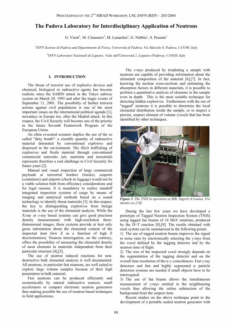
PROCEEDINGS OF THE 2ND SIRAD WORKSHOP, LNL-INFN (REP) – 203/2004
88
The Padova Laboratory for Interdisciplinary Application of Neutrons
G. Viesti1, M. Cinausero2, M. Lunardon1, G. Nebbia1, S. Pesente1
1INFN Sezione di Padova and Dipartimento di Fisica, Università di Padova, Via Marzolo 8, Padova, I-35100, Italy
2INFN Laboratori Nazionali di Legnaro, Viale dell'Università 2, Legnaro (Padova), I-35020, Italy
I. INTRODUCTION
The threat of terrorist use of explosive devices and chemical, biological or radioactive agents has become realistic since the SARIN attack in the Tokyo subway system on March 20, 1995 and after the tragic events of September 11, 2001. The possibility of further terrorist actions against civil populations is one of the most important issues on the international political agenda [1], nowadays in Europe too, after the Madrid attack. In this respect, the Civil Security will become one of the priority in the future Seventh Framework Program of the European Union.
An often evocated scenario implies the use of the so called "dirty bomb": a sizeable quantity of radioactive material detonated by conventional explosive and dispersed in the environment. The illicit trafficking of explosives and fissile material through conventional commercial networks (air, maritime and terrestrial) represents therefore a real challenge to Civil Security for future years [2].
Manual and visual inspection of large commercial payloads at terrestrial borders (trucks), seaports (containers) and airports (check-in luggage) would not be a viable solution both from efficiency considerations and for legal reasons. It is mandatory to realize standoff integrated inspection systems of cargo by means of imaging and analytical methods based on a sound technology to identify threat materials [3]. In this respect, the key to distinguishing explosives from benign materials is the use of the elemental analysis. While the X-ray or γ-ray based systems can give good precision density measurements with high-resolution three-dimensional images, these systems provide at best only gross information about the elemental content of the inspected item (low Z as a function of high Z discrimination). Neutron interrogation, on the contrary, offers the possibility of measuring the elemental density of most elements in materials independent from their particular structure [4],[5].
The use of neutron induced reactions for non-destructive bulk elemental analysis is well documented. All neutrons, in particular fast neutrons, are well suited to explore large volume samples because of their high penetration in bulk material.
Fast neutrons can be produced efficiently and economically by natural radioactive sources, small accelerators or compact electronic neutron generators thus making possible the use of neutron based techniques in field applications.
The γ-rays produced by irradiating a sample with neutrons are capable of providing information about the elemental composition of the material [6],[7]. In fact, knowing the nuclear cross-sections and estimating the absorption factors in different materials, it is possible to perform a quantitative analysis of elements in the sample even in depth. This is the most suitable technique for detecting hidden explosives. Furthermore with the use of "tagged" neutrons it is possible to determine the local elemental distribution inside the sample, or to inspect a precise, suspect element of volume (voxel) that has been identified by other techniques.
Figure 1. The TNIS in operation at IRB, Zagreb (Croatia). For details see [10].
During the last few years we have developed a prototype of Tagged Neutron Inspection System (TNIS) using tagged fan beams of 14 MeV neutrons, produced by the D+T reaction [8],[9]. The results obtained with such system can be summarized in the following points. 1) The use of tagged neutron beams improves the signal to noise ratio by electronically selecting the γ-rays from the voxel defined by the tagging detector and by the neutron time of flight. 2) The size of the inspected voxel strongly depends on the segmentation of the tagging detector and on the overall time resolution of the α-γ coincidences. Fast γ-ray detectors and fast and highly segmented α particle detection systems are needed if small objects have to be interrogated. 3) The use of fan beams allows the simultaneous measurement of γ-rays emitted in the neighbouring voxels thus allowing the online subtraction of the background from the suspect item.
Recent studies on the above technique point to the development of a portable sealed neutron generator with

PROCEEDINGS OF THE 2ND SIRAD WORKSHOP, LNL-INFN (REP) – 203/2004
89
the neutron tagging detector embedded into the system. Such development has been successfully performed in a collaborative project between the Physics Department of the Padova University, INFN and EADS-SODERN [10]. In the meantime, the α particle detector selected for this application has been tested in our inspection system now in operation at the Neutron Generator Laboratory of the Ruder Boskovic Institute (IRB) in Zagreb (Croatia) [11], as shown in Fig.1. With our inspection system it is possible to identify explosive devices hidden in the luggage or even to analyze the TNT charge inside a large anti-tank land mine, as demonstrated in Fig.2.
This research activity will continue in the near future in the framework of international collaborations. In the meantime, a Laboratory for Interdisciplinary Application of Neutrons is being setting up by the Padova University. It will be in operation in a dedicated area inside the INFN National Laboratory of Legnaro (Padova, Italy) and is described in the following sections.
Figure 2. The γ-ray spectra of a TMA-1A mine hidden in the luggage.
II. THE PADOVA LABORATORY FOR INTERDISCIPLINARY APPLICATION
OF NEUTRONS
Within the EXPLODET project, two shielded rooms were prepared, licensed to host neutron sources up to 107 n/s inside the so-called "Laboratorio di Alta Energia" (LAE) that belongs to the INFN Padova Section. A photograph of the shielded areas is reported in Fig.3.
In one room, a sealed 252Cf source (originally 107 n/s) is in operation since a number of years. The source is hosted in a polyethylene cube that acts as a biological shield, as shown in Fig.4. A pneumatic piston allows the extraction of the source that normally is used in a hybrid moderator to induce thermal neutron capture reaction on different samples. The γ-rays produced in this way are detected in a γ-ray detection system employing a NaI(Tl) scintillator and a HPGe detector. Both detectors are inserted in anti-coincidence shields to reduce the background from the neutron source and to simplify the analysis of the γ-ray spectra by suppressing the escape peaks. This prompt γ-ray activation analysis system is under development and is used also in connection with educational and training activities mentioned below.
Figure 3. The Laboratory for Interdisciplinary Application of Neutrons inside the LAE building at the INFN National Laboratory of Legnaro.
Figure 4. The 252Cf source housing and the hybrid polyethylene moderator when used to detect buried objects.
In the second area a sealed neutron generator system from SODERN (France) will be installed. Such system allows the use of both D+D and D+T neutron producing heads so that mono-energetic neutrons having energy of 2.5 MeV and 14 MeV will be available. Moreover, the D+T neutron head contains an embedded α particle detector that is used to obtain a tagged neutron beam.
It is important to note that our laboratory is licensed to run neutron sources up to 107 n/s, consequently the available neutron producing head will be in any case used within such constrain. The sealed neutron generator will be installed and commissioned before summer 2004.
III. PLANNED ACTIVITIES
A number of experimental activities are already planned inside the Padova Laboratory for Interdisciplinary Application of Neutrons, as continuation of previous programs.
The activities related to the Civil Security will continue under two major programs.
PROCEEDINGS OF THE 2ND SIRAD WORKSHOP, LNL-INFN (REP) – 203/2004
90
1) A project entitled "Control of illicit trafficking of threat materials" has been recently approved within the NATO Science for Peace Program. It is based on a collaboration between INFN and the Ruder Boskovic Institute in Zagreb (Croatia). 2) The project EURITRACK (EURopean Illicit TRAfficking Countermeasure Kit) is started on October 1, 2004 within the IST part of the 6th Framework Program. This is a 3 year project under the coordination of the CEA (France). The Italian participation to EURITRACK is responsible to one of the major project work package.
Moreover, a training activity on application of nuclear techniques in the detection of explosives will start in October 2004 within the IAEA programs.
Finally, the existing facilities are already used for student experimental activities related to the thesis activity at the end of the "Laurea Triennale in Fisica".
The planned researches will not saturate the possible activities in our laboratory: as in the past, we will be open to external users too. It is worth mentioning that external users have already performed material irradiations or detector tests. No special formalities are required to use the existing facilities, with the exception of the general requirements to access the INFN National Laboratory of Legnaro and the safety instructions related to the radiation hazard. ____________________ [1] "Making the nation safer, the role of science and technology in
countering terrorism", The National Academy Press, Washington DC, USA, 2002. On line available: www.nap.edu.
[2] M. Bunn, J. P. Holdrenn and A. Wier, "Securing nuclear weapons and materials, seven steps for immediate actions", Belfer Centre for Science and International Affairs, J. F. Kennedy School of Government, Harvard University, 2002. On line available: www.nti.org.
[3] T. Gozani, Nucl. Instr. Meth., B213 (2004) 460. [4] J. Rynes et al., Nucl. Instr. Meth., A422 (1999) 895. [5] I. V. Chuvilo et al., Nucl. Instr. Meth., B139 (1998) 298. [6] G. Vourvopoulos et al., Talanta, 54 (2001) 459, and references
therein. [7] P. Bach et al., Nucl. Instr. Meth., B79 (1993) 605. [8] M. Lunardon et al., Nucl. Instr. Meth., B213 (2004) 544. [9] G. Nebbia et al., Proceedings of the 17th International Conference
on Application of Accelerators in Research and Industry, edited by J. L. Duggan and I. L. Morgan, AIoP CP680, (2002) 487.
[10] S. Pesente, "Development of inspection systems using 14 MeV tagged neutron beams", PhD Thesis, Padova University, 2003.
[11] S. Pesente et al., Nucl. Instr. Meth., A531 (2004) 657. [12] L. Zuin et al., Nucl. Instr. Meth., A449 (2000) 416. [13] M. Cinausero et al., "Development of a thermal neutron sensor for
humanitarian de-mining", Applied Radiation and Isotopes, in press.
PROCEEDINGS OF THE 2ND SIRAD WORKSHOP, LNL-INFN (REP) – 203/2004
91
The SIRAD irradiation facility for bulk damage and Single Event Effect studies
A. Candelori1, D. Bisello1, P. Giubilato1, A. Kaminski1, D. Pantano1, R. Rando1, M. Tessaro1, J. Wyss2
1INFN Sezione di Padova and Dipartimento di Fisica, Università di Padova, Via Marzolo 8, Padova, I-35131, Italy
2D.I.M.S.A.T., Università di Cassino, Via Di Biasio 43, Cassino (Frosinone), I-03043, Italy
I. INTRODUCTION
The study of the effects on semiconductor devices due to natural and artificial radiation is an important and lively field in scientific and technological research. In particular radiation tolerance is a fundamental issue for electronic devices and systems in many applications such as Nuclear Plants, Space Research, Telecommunications, Avionics, Medical Imaging, and High Energy Physics [1].
Radiation damage in semiconductor devices occurs when there is energy deposition in a sensitive part of the device in form of atomic displacement and/or ionization [2]. The energy deposited as atomic displacement generates point defects (i.e., vacancies and interstitials) as well as cluster defects (i.e., high density defect regions) in the semiconductor lattice, causing the so-called "bulk damage". The bulk damage is relevant if the substrate is a sensitive part of the device itself, such as in diodes, particle detectors, solar cells, light-emitting diodes and bipolar transistors.
The energy deposited in form of ionization generates electron-hole pairs. High electron-hole pair densities in the semiconductor bulk (and to a less intent in SiO2) can influence the device functionality if the charge is generated in a high electric field region and/or it is collected at a sensitive node of the circuit. These effects are generally due to the ionization induced by a single ion along its track and are called "Single Event Effects" (SEE). Single ions are able to induce device functionality failures, such as Single Event Upset (SEU) and Single Event Functionality Interrupt (SEFI) in digital electronics, and also lead to permanent device damage, such as Single Event Burnout (SEB) in power diodes, Single Event Gate Rupture (SEGR) in power MOSFET and Single Event Latch-up (SEL) in CMOS technologies.
Bulk damage and SEE studies are routinely addressed at the SIRAD irradiation facility of the INFN National Laboratory of Legnaro (Padova, Italy) by Universities and Industrial groups, involved in the study of the radiation hardness of semiconductor devices and electronic systems for High Energy Physics and Space applications. In this contribution we will report on the SIRAD irradiation facility by describing the proton and ion beam characteristics, the dosimeter systems for particle fluence measurements as well as the scientific and technological solutions implemented to accommodate electronic radiation hardness tests.
II. BEAMS AVAILABLE AT THE SIRAD IRRADIATION FACILITY
The Tandem-XTU accelerator at the INFN National Laboratory of Legnaro is an electrostatic Van de Graaff type: two stripper stations are used in order to achieve high ion energies as shown in Fig.1. Normally, the extracted beam is continuous but pulsed beams are also possible. The maximum operating voltage is 15 MV and available ions range from 1H (30 MeV) to 197Au (1.4 MeV/a.m.u.). The energy, expressed in MeV, of the ions at the exit of the Tandem with two strippers is:
E = EInj + V0 × (1 + q1×f + q2×(1-f)) (1)
where EInj=0.18 MeV is the energy of the negative charged ion injected from the source into the Tandem, V0=11-15 MV is the Tandem operating voltage, f=0.25, and q1 is the positive charge of the ion expressed in units of the electron charge after the first stripper foil located at the terminal. The charge q2>q1 is the ion charge after the second stripper foil located downstream of the first one. The second stripper foil can be excluded, in which case the energy of the ions is E = Einj + V0 × (1 + q1).
The beam at the Tandem output is not monochromatic due to the different possible q1 and q2 ion charge states. The ion energy delivered to the experimental beam lines can be changed without varying the Tandem operating voltage selecting only one of the many possible ion charge states by magnetic momentum analysis. Finally, the switching magnet after the analyzing magnet deviates the monochromatic beam into the experimental channels.
The Tandem-XTU accelerator services 3 experimental halls and 10 beam lines: the SIRAD beam line is the +70° in hall 1, as schematically shown in Fig.1.
The characteristics of the typical ion beams available at the SIRAD irradiation facility are reported in Table I: the energy values refer to the most probable q1 and q2 charge state, obtained with two stripper stations and with the Tandem operating at 14 MV, while the surface ion LET and range in silicon have been calculated by SRIM [3]. At present when using 197Au beams in SIRAD the operating voltage is typically lowered to 11.6 MV due to a constraint in the maximum magnetic field to deviate the beam into the line at 70o. The ion species reported in Table I have been selected in order to minimize the time required for the ion source change during SEE tests. When possible two multi-sources (the first including O, Si, Ni and Ag; the second including F, Cl, Br, and I) are
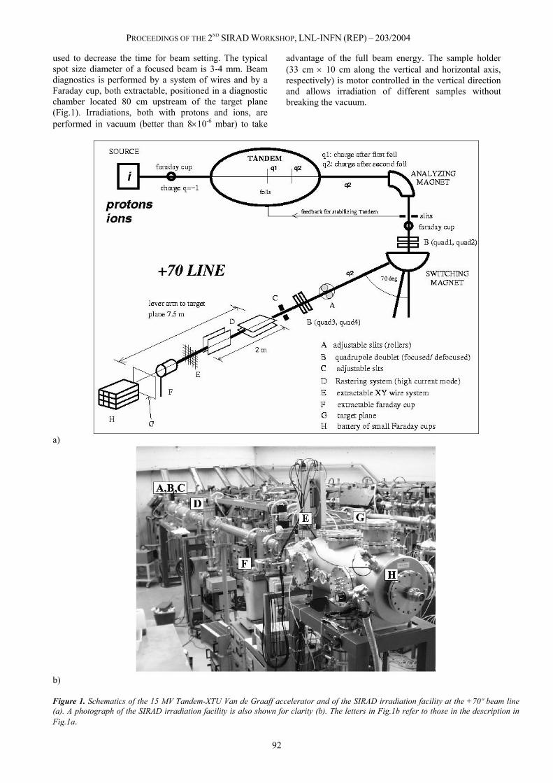
PROCEEDINGS OF THE 2ND SIRAD WORKSHOP, LNL-INFN (REP) – 203/2004
92
used to decrease the time for beam setting. The typical spot size diameter of a focused beam is 3-4 mm. Beam diagnostics is performed by a system of wires and by a Faraday cup, both extractable, positioned in a diagnostic chamber located 80 cm upstream of the target plane (Fig.1). Irradiations, both with protons and ions, are performed in vacuum (better than 8×10⁻⁶ mbar) to take
advantage of the full beam energy. The sample holder (33 cm × 10 cm along the vertical and horizontal axis, respectively) is motor controlled in the vertical direction and allows irradiation of different samples without breaking the vacuum.
a)
b) Figure 1. Schematics of the 15 MV Tandem-XTU Van de Graaff accelerator and of the SIRAD irradiation facility at the +70º beam line (a). A photograph of the SIRAD irradiation facility is also shown for clarity (b). The letters in Fig.1b refer to those in the description in Fig.1a.

PROCEEDINGS OF THE 2ND SIRAD WORKSHOP, LNL-INFN (REP) – 203/2004
93
TABLE I. CHARACTERISTICS OF THE TYPICAL ION BEAMS AVAILABLE AT THE SIRAD IRRADIATION FACILITY WITH THE TANDEM OPERATING AT
14 MV.
Ion species
Energy (MeV)
q1 q2 Range in Si (µm)
Surface LET in Si (MeV×cm2/mg)
1H 28.18 1 1 4390 0.02 7Li 56.18 3 3 378 0.37 11B 80.68 4 5 195 1.01 12C 94.68 5 6 171 1.49 16O 108.68 6 7 109 2.85 19F 122.68 7 8 99.3 3.67 28Si 157.68 8 11 61.5 8.59 32S 171.68 9 12 54.4 10.1
35Cl 171.68 9 12 49.1 12.5 48Ti 196. 18 10 14 39.3 19.8 51V 196.18 10 14 37.1 21.4 58Ni 220.68 11 16 33.7 28.4 63Cu 220.68 11 16 33.0 30.5 74Ge 231.18 11 17 31.8 35.1 79Br 241.68 11 18 31.3 38.6
107Ag 266.18 12 20 27.6 54.7 127I 276.68 12 21 27.9 61.8
197Au 275.68 13 26 23.4 81.7
III. HIGH FLUX IRRADIATION SETUP
In order to irradiate a large target, the focused proton or ion beam is rastered by a system of vertical and horizontal deflection plates with linearly ramped voltages produced by IBA (Louvain-la-Neuve, Belgium). The rastering system permits a uniform irradiation (better than 5%) over a fiducial area of 5×5 cm2 on the target plane. On-line monitoring of the beam current and uniformity on the target is provided by a square battery of 3×3 small Faraday cups, located behind the target plane (sample holder), as shown in Fig.2.
Irradiation Chamber
Ion or proton beam
3x3 Faraday cup batterySample holder
5 cm
5x5 cm2aperture
Device under test
Figure 2. The on-line beam monitoring for rastered proton and ion beams by the 3×3 battery of Faraday cups positioned behind the DUT: side view of the experimental setup. The aperture of each Faraday cup is 0.6×0.6 cm2. The figure is not drawn to scale.
This configuration is suitable for radiation tests at beam currents higher than 100 pA/cm2 and is currently used for proton induced bulk damage studies in silicon detectors for High Energy Physics experiments [4]-[6] or in solar cells for satellites. The thickness of silicon detectors for High Energy Physics is typically 300-500 µm, significantly lower than the range in Si of protons available at SIRAD. In addition the proton energy loss
across these silicon thicknesses is ≈1-2 MeV [3], which ensures a uniform damage throughout the device bulk and allows online proton flux measurements with the Faraday cup system.
The maximum proton currents routinely available (≈20-25 nA) are limited only by radioprotection constraints on the activation levels of the beam line elements: with such values uniform fluences up to 1014 protons/cm2 over the 5×5 cm2 fiducial area can be achieved in ≈5 hours. On the contrary, the maximum ion currents (≈100-1000 nA) are limited only by the source characteristics. Radiation damage studies in thin oxides at high doses up to 500 Mrad(Si) have been performed with focused ion beams using this experimental setup [7]-[10].
IV. LOW FLUX IRRADIATION SETUP
The low ion fluxes (102-105 ions/(cm2×s)) necessary for SEE studies in electronic devices and systems are obtained by closing machine collimators to achieve low beam currents (0.3-1 nA) and by defocusing the beam on the target plane by adjusting the SIRAD quadrupole doublet (see Fig.1). The quadrupole doublet is positioned before the rastering system, which normally is not used in defocused beam irradiations.
The ion fluxes for SEE tests are below the sensitivity of the Faraday cups and are consequently monitored by a different system, shown in Fig.3. A battery of 4 silicon diodes, called "fixed diodes", are mounted on a fixed frame with a 2×2 cm2 central aperture: the diodes are placed immediately upstream of the sample holder and surround the device under test (DUT). Another group of 4 diodes, called "mobile diodes", are mounted on the mobile sample holder and can exchange position with the DUT within the 2×2 cm2 aperture. During beam setup and ion flux uniformity measurements the wide ion beam illuminates the fixed and mobile diodes. The DUT is then moved into position for SEE testing while the fixed diodes continue to be exposed to the beam. The ratios between the fluxes on the fixed and mobile diodes are measured during the beam setup procedure before every run. The shape of the defocused beam, continuously monitored by the fixed diodes, does not change during normal irradiation conditions and hence the particle flux on the DUT can be determined by monitoring the flux on the fixed diodes. In principle one fixed and one mobile diode would be suitable for the calibration procedure in most applications, but this setup, with multiple fixed and mobile diodes, allows more precise measurements of the beam uniformity within the 2×2 cm2 DUT irradiation area.
Each silicon diode is 300 µm thick with a 0.5×0.5 cm2 sensitive area surrounded by a multi-guarded structure in order to increase the device breakdown voltage (≈400 V). In operational conditions each diode is over depleted (100-200 V) and connected to a read-out electronic channel for data acquisition of the ion impact signals, as shown in Fig.4. The first stage of the read-out electronics is a charge integrator (preamplifier) followed by a CR-RC shaper. The preamplifier and shaper have
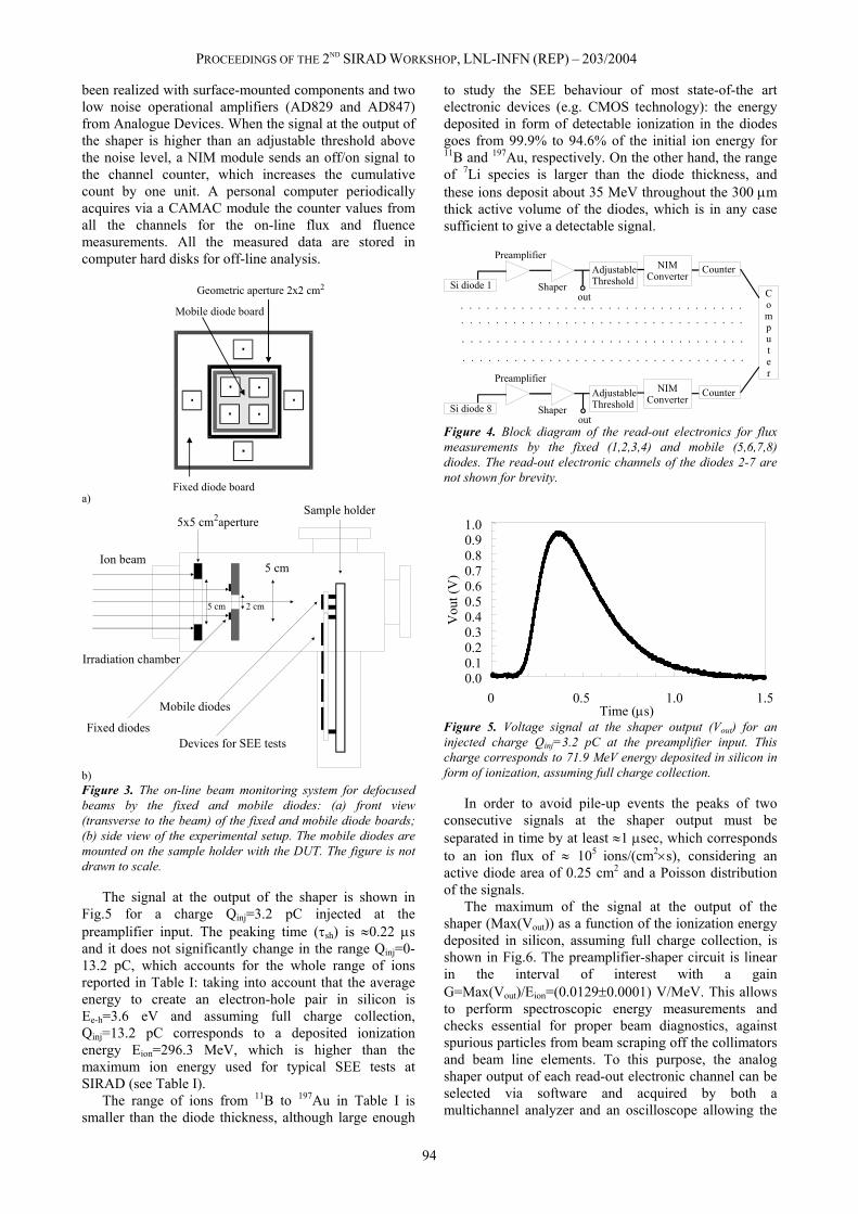
PROCEEDINGS OF THE 2ND SIRAD WORKSHOP, LNL-INFN (REP) – 203/2004
94
been realized with surface-mounted components and two low noise operational amplifiers (AD829 and AD847) from Analogue Devices. When the signal at the output of the shaper is higher than an adjustable threshold above the noise level, a NIM module sends an off/on signal to the channel counter, which increases the cumulative count by one unit. A personal computer periodically acquires via a CAMAC module the counter values from all the channels for the on-line flux and fluence measurements. All the measured data are stored in computer hard disks for off-line analysis.
Mobile diode board
Fixed diode board
Geometric aperture 2x2 cm2
a)
5 cm 2 cm
Irradiation chamber
Ion beam
Sample holder
5 cm
5x5 cm2aperture
Devices for SEE testsFixed diodes
Mobile diodes
b) Figure 3. The on-line beam monitoring system for defocused beams by the fixed and mobile diodes: (a) front view (transverse to the beam) of the fixed and mobile diode boards; (b) side view of the experimental setup. The mobile diodes are mounted on the sample holder with the DUT. The figure is not drawn to scale.
The signal at the output of the shaper is shown in Fig.5 for a charge Qinj=3.2 pC injected at the preamplifier input. The peaking time (τsh) is ≈0.22 µs and it does not significantly change in the range Qinj=0-13.2 pC, which accounts for the whole range of ions reported in Table I: taking into account that the average energy to create an electron-hole pair in silicon is Ee-h=3.6 eV and assuming full charge collection, Qinj=13.2 pC corresponds to a deposited ionization energy Eion=296.3 MeV, which is higher than the maximum ion energy used for typical SEE tests at SIRAD (see Table I).
The range of ions from 11B to 197Au in Table I is smaller than the diode thickness, although large enough
to study the SEE behaviour of most state-of-the art electronic devices (e.g. CMOS technology): the energy deposited in form of detectable ionization in the diodes goes from 99.9% to 94.6% of the initial ion energy for
11B and 197Au, respectively. On the other hand, the range of 7Li species is larger than the diode thickness, and these ions deposit about 35 MeV throughout the 300 µm thick active volume of the diodes, which is in any case sufficient to give a detectable signal.
Si diode 1
Preamplifier
Shaper
Counter
Computer
AdjustableThreshold
NIMConverter
Si diode 8
Preamplifier
Shaper
CounterNIMConverter
. . . . . . . . . . . . . . . . . . . . . . . . . . . . . . . . .
. . . . . . . . . . . . . . . . . . . . . . . . . . . . . . . . .
. . . . . . . . . . . . . . . . . . . . . . . . . . . . . . . . .
. . . . . . . . . . . . . . . . . . . . . . . . . . . . . . . . .
out
out
AdjustableThreshold
Figure 4. Block diagram of the read-out electronics for flux measurements by the fixed (1,2,3,4) and mobile (5,6,7,8) diodes. The read-out electronic channels of the diodes 2-7 are not shown for brevity.
0.00.10.20.30.40.50.60.70.80.91.0
0 0.5 1.0 1.5Time (µs)
Vou
t(V
)
Figure 5. Voltage signal at the shaper output (Vout) for an injected charge Qinj=3.2 pC at the preamplifier input. This charge corresponds to 71.9 MeV energy deposited in silicon in form of ionization, assuming full charge collection.
In order to avoid pile-up events the peaks of two consecutive signals at the shaper output must be separated in time by at least ≈1 µsec, which corresponds to an ion flux of ≈ 105 ions/(cm2×s), considering an active diode area of 0.25 cm2 and a Poisson distribution of the signals.
The maximum of the signal at the output of the shaper (Max(Vout)) as a function of the ionization energy deposited in silicon, assuming full charge collection, is shown in Fig.6. The preamplifier-shaper circuit is linear in the interval of interest with a gain G=Max(Vout)/Eion=(0.0129±0.0001) V/MeV. This allows to perform spectroscopic energy measurements and checks essential for proper beam diagnostics, against spurious particles from beam scraping off the collimators and beam line elements. To this purpose, the analog shaper output of each read-out electronic channel can be selected via software and acquired by both a multichannel analyzer and an oscilloscope allowing the

PROCEEDINGS OF THE 2ND SIRAD WORKSHOP, LNL-INFN (REP) – 203/2004
95
on-line monitor of the ion beam pulse height (energy) distribution.
Ion impacts damage the fixed and mobile diodes and cause: 1) an increase of the diode leakage current and consequently an increase of shot noise; 2) a decrease of the charge collection efficiency and consequently a decrease of the signal at the input of the read-out electronics. The charge collection loss can be partially compensated by increasing the diode reverse bias voltage, which in any case can not be larger than the diode breakdown voltage. The continuous online monitoring of the analog signal at the output of the shaper allows one to maintain full detection efficiency, necessary for the correct determination of the beam flux, and to determine when the diodes need to be replaced as a consequence of excessive damage. The maximum fluence for diodes operating in flux measurements is limited typically in the range 109-1011 ions/cm2, depending on the impinging particle species and energies. This experimental setup for low ion flux measurements has been successfully used for SEE studies on semiconductor devices and electronic systems: heavy ion effects in power diodes [11] and thin gate oxides [12]; SEU and Latch-up tests on High Energy Physics read-out electronic chips [13],[14], Field Programmable Gate Array (FPGA) devices [15] and Floating Gate memory cells [16].
0.0
1.0
2.0
3.0
4.0
5.0
0 50 100 150 200 250 300
Eion (MeV)
Max
(Vou
t)(V
)
G=0.0129±0.0001 V/MeV
Figure 6. Maximum of the signal at the shaper output (Vout) as a function of the ionization energy deposited in Si assuming full charge collection.
V. CONCLUSIONS
The SIRAD facility at the 15 MV Tandem-XTU accelerator of the INFN National Laboratory of Legnaro (Padova, Italy) was constructed in 1996 as a proton irradiation facility for radiation damage studies of silicon detectors for High Energy Physics experiments. The flexibility of the Tandem-XTU accelerator and the beam line optics were quickly recognized and exploited to expand the program of SIRAD to include heavy-ion irradiations for Single Event Effect studies on electronics components and systems for High Energy Physics experiments and Space applications.
The scientific contributions of the researches at SIRAD in the very wide field of proton and ion radiation effects in semiconductor detectors, devices and systems, unique in Italy, have been very successful. The facility is
next to undergo a major upgrade that will include a unique Ion Electron Emission Microscope (IEEM) for studying Single Event Effects with micrometric spatial resolution.
VI. ACKNOWLEDGEMENTS
We would like to thank the director of the INFN National Laboratory of Legnaro, G. Fortuna, for his support and encouragement in our research activity. We also thank L. Corradi, Tandem Scientific Coordinator, and A. Dainelli, Tandem Operation Coordinator. Last but not least we sincerely thank all the Tandem operators, the Ion Source (G. Binelle and F. Scarpa) and Radioprotection (D. Zafiropoulos and G. Scarabottolo) groups for their patience and precious help. ___________________ [1] A. Holmes-Siedle and L. Adams, "Handbook of radiation effects",
Oxford University Press, 2002. [2] T. P. Ma and P. V. Dressendorfer, "Ionizing radiation effects in
MOS devices and circuits", John Wiley & Sons, 1989. [3] J. F. Ziegler, "SRIM, Stopping and range of ions in matter", On
line available: http://www.srim.org. [4] J. Wyss et al., Nucl. Instr. Meth., A457 (2001) 595. [5] D. Bisello et al., IEEE Trans. Nucl. Sci., 48 (2001) 1020. [6] A. Candelori et al., IEEE Trans. Nucl. Sci., 48 (2001) 2270. [7] L. Larcher et al., IEEE Trans. Nucl. Sci., 46 (1999) 1553. [8] M. Ceschia et al., IEEE Trans. Nucl. Sci., 47 (2000) 566. [9] M. Ceschia et al., IEEE Trans. Nucl. Sci., 47 (2000) 2648. [10] A. Candelori et al., IEEE Trans. Nucl. Sci., 48 (2001) 1735. [11] G. Busatto et al., "Effects of heavy ion impact on power diodes,"
Proceedings of RADECS 1999, Abbaye de Fontevraud, France, 13-19 September 1999.
[12] A. Cester et al., IEEE Trans. Nucl. Sci., 48 (2001) 2093. [13] E. Noah et al., Nucl. Instr. Meth., A492 (2002) 434. [14] M. Sugizaki et al., "SEE test of the LAT tracker front end ASIC",
GLAST LAT Technical Document, LAT-TD-00333, 2001. [15] M. Bellato et al., "Ion beam testing of SRAM-based FPGA's",
Proceedings of RADECS 2001, Grenoble, France, 10-14 September 2001.
[16] G. Cellere et al., IEEE Trans. Nucl. Sci., 48 (2001) 2222.

PROCEEDINGS OF THE 2ND SIRAD WORKSHOP, LNL-INFN (REP) – 203/2004
96
The Ion Electron Emission Microscope for Single Event Effect studies at SIRAD
D. Bisello1, P. Giubilato1, M. Nigro1, R. Rando1, J. Wyss2, A. Candelori1
1INFN Sezione di Padova and Dipartimento di Fisica, Università di Padova, Via Marzolo 8, Padova, I-35131, Italy
2D.I.M.S.A.T., Università di Cassino, Via Di Biasio 43, Cassino (Frosinone), I-03043, Italy.
I. THE IEEM UPGRADE
The SIRAD irradiation facility is dedicated to radiation damage studies in silicon detectors, semiconductor microelectronic devices and systems for High Energy Physics and Space applications [1]. Device characterizations such as Single Event Effect (SEE) cross-section measurements are routinely performed using a wide selection of energetic ion species. A very important part of the research and validation program at SIRAD is the study of SEE in various Application Specific Integrated Circuits (ASIC) and, more generally, state-of-the-art commercial devices such as FPGA, SDRAM, FLASH memories and power devices.
In order to extend this successful program by including micrometric characterizations of the device under test (DUT), the SIRAD group is developing Ion Electron Emission Microscopy (IEEM) capabilities. The IEEM technique is somewhat complementary to the consolidated nuclear microprobe technique that builds up sensitivity maps with lateral resolutions of the order of 0.5-1.0 µm by moving a micro-focused beam spot systematically across the DUT with micrometric precision. In the IEEM innovative technique [2], a broad (non-focused) ion beam irradiates the part of the DUT that is moved into the field of view of the electron emission microscope whose area has a diameter of 250 µm. The position of each single ion impact in the field of view is then reconstructed with micrometric resolution by collecting secondary electrons emitted from the target DUT surface and transferring and focusing them, by means of the system of electrostatic lenses that make up the microscope, onto a fast two-dimensional electron detector [3]. For SEE or time resolved Ion Beam Induced Charge Collection (IBICC) studies the X,Y transverse coordinates and the time T of the random ion impacts are then correlated with events induced in a DUT to establish a sensitivity map.
II. THE AXIAL IEEM
In the IEEM configuration at SIRAD the ion beam passes axially through a commercial photon electron emission microscope (PEEM) to impact normally the DUT surface, as shown in Fig.1. The secondary electrons emitted during each ion impact are collected and transferred by the microscope, a series of electrostatic lenses, onto a large annular Micro-Channel Plate (MCP) electron multiplier placed at the focal plane. The amplified electronic signal generated by the MCP excites
a fast phosphor screen to create photons which are then extracted from the irradiation chamber by means of a mirror and a quartz window. The optical image is focused by a system of lenses onto an image intensifier and a photon Position Sensitive Detector (PSD), for the determination of the position of the luminous spot.
Figure 1. A schematic of the axial IEEM to be installed downstream of the SIRAD irradiation chamber.
The standard detectors used for the PEEM surface analysis technique are commercial two-dimensional CCD, but have long readout times that limit the useful ion fluxes. Consider a typical bi-dimensional CCD sufficient to match the resolution of the IEEM: for a one-output 1024×1024 array the frame rate is about 30 frames per second (total data rate 40 MHz). To avoid too many frames with multiple hits the ion fluxes in the field of view of the IEEM must be of the order of 10 ion impacts/s. This limits the use of CCD arrays in SEE studies to those devices that present a large total cross-section in the field of view. Rates of hundreds of ions per second in the IEEM field of view are in fact needed to perform most small SEE cross-section measurements in a reasonable amount of time. The SIRAD IEEM group has developed two solutions that ensure optimal flexibility for SEE studies and high spatial resolution with repetition rates two orders of magnitude higher than those of CCD arrays.
The first solution developed is based on a commercial 2×2 cm2 UV-enhanced semiconductor high linearity Position Sensitive Device (PSD) which is based on the lateral-effect photodiode principle: the charge produced by impacting photons (68% photon to electron-hole conversion efficiency) is split by a thin resistive layer into four charges; the position of the luminous spot is then determined by relative weights of the signals at the

PROCEEDINGS OF THE 2ND SIRAD WORKSHOP, LNL-INFN (REP) – 203/2004
97
four electrodes, two per transverse dimension. The present setup acquires a few 104 events/s. A drawback of this system is that the lateral resolution depends on the intensity of the luminous spot and to reach a lateral resolution that equals the theoretical one of the IEEM (i.e., 0.6 µm) requires a large number of photons and, consequently, an MCP with a high gain (few 108). Rather than degrade immediately the IEEM resolution by substituting the two-stack MCP detector with a high gain multi-stack MCP, we chose to use a high resolution image intensifier placed outside the irradiation chamber in front of the PSD. The working PSD system was presented in detail at the ICNMTA 2002 conference [4].
The second fast photon position detector system we have developed, presented in detail at the IBA2003 conference [5], is based on a beam splitter and a system of lenses to split the image of the luminous spot produced by the IEEM phosphor. The two images are then transported and focused onto two orthogonal planes. For each optical path the luminous spot is focused into a blade shape by an additional cylindrical lens. The two cylindrical lenses and consequently the luminous blades along the two paths are mutually orthogonal. Each luminous blade is then intercepted by a linear CCD with 1024 pixels placed at 90o with respect to the axis of the cylindrical lens. The linear CCDs at the end of the two optical paths are mutually orthogonal and each sensor independently registers one transverse coordinate of the original luminous spot and the coordinate pair is obtained by correlating the frames from the two sensors. This bi-linear CCD system has a repetition rate that is similar to that of the PSD system described above, but it presents two very important advantages: due to the pixel (digital) nature of the CCD detector the spatial resolution is essentially independent from the intensity of the luminous spot, unlike the PSD analogue system, and the image intensifier stage is no longer necessary.
For both detector systems the maximum sustainable ion rate impact is a few 104 Hz, i.e. two orders of magnitude faster than those achievable with conventional two-dimensional CCD arrays, ensuring great flexibility for SEE and time resolved IBICC studies.
III. CONCLUSIONS
The SIRAD group has developed an axial Ion Electron Emission Microscope (IEEM) system by which it is possible to obtain time resolved images of the ion impacts on a DUT; i.e. a time ordered list of the X,Y coordinates of the ion impact points. A prototype system, on standby for the installation in the SIRAD ion beam line, is operating in PEEM configuration. The first ion beam tests will be performed using a Single Event Upset detection test system based on a SDRAM. For a 250 µm diameter field of view on the DUT surface, ion impact lateral resolutions better than 1 µm are expected with the bi-linear CCD system. The resolutions obtained with the PSD system are expected to be slightly worse (≈1 µm). ____________________ [1] J. Wyss et al., Nucl. Instr. Meth., A462 (2001) 426. [2] B. L. Doyle et al., Nucl. Instr. Meth., B158 (1999) 6.
[3] D. Bisello et al., Nucl. Instr. Meth., B181 (2001) 254. [4] D. Bisello et al., Nucl. Instr. Meth., B210 (2003) 142. [5] D. Bisello et al., Nucl. Instr. Meth., B219 (2004) 1000.

98
Proceedings of the 2nd SIRAD Workshop
Editor A. Candelori
LNL-INFN (REP) 203/2004
ISBN 88-7337-007-1
http://sirad.pd.infn.it
INFN Sezione di Padova
Printed by Copisteria Belzoni, Padova, Italy
December 2004


Proceedings of the 2nd SIRAD Workshop LNL-INFN (REP) 203/2004 ISBN 88-7337-007-1 http://sirad.pd.infn.it