Oracle Cache Fusion Cache Fusion Concepts, Data Block Shipping, and Recovery with Cache Fusion.
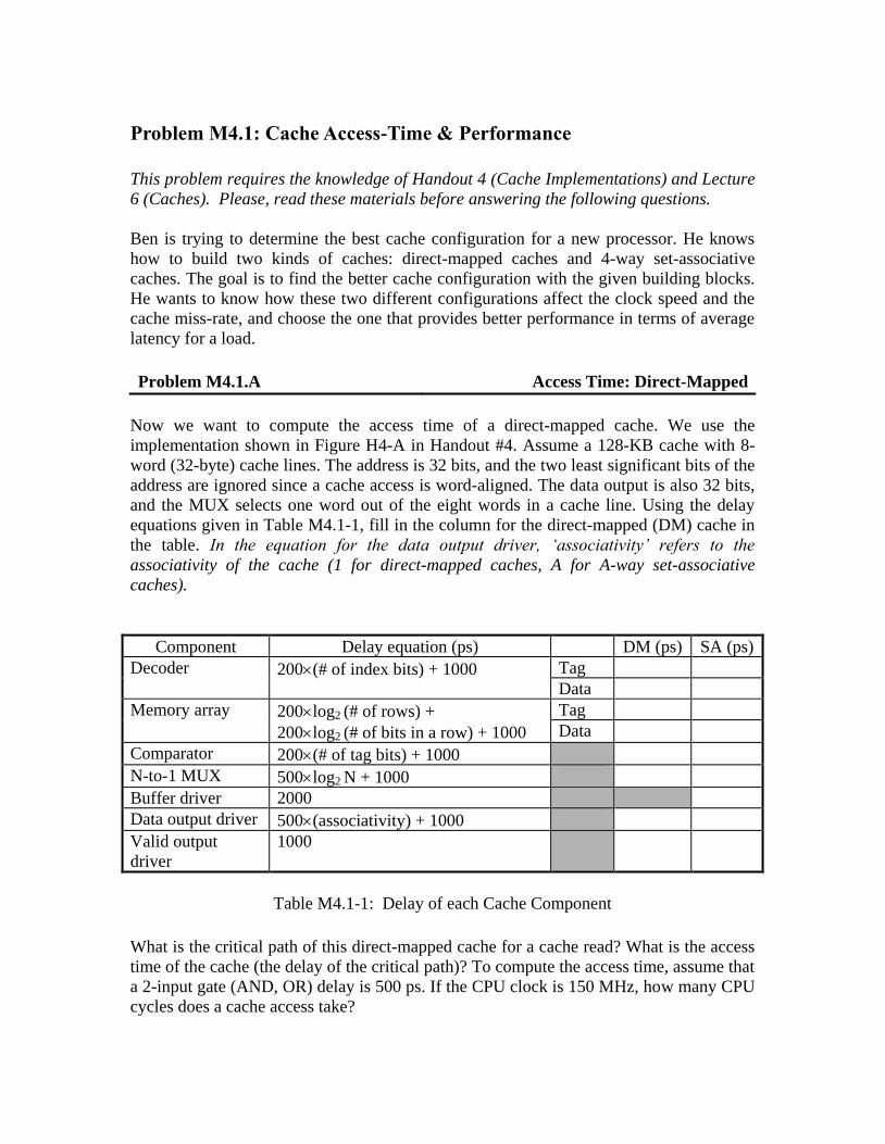
Problem M4.1: Cache Access-Time & Performance
This problem requires the knowledge of Handout 4 (Cache Implementations) and Lecture
6 (Caches). Please, read these materials before answering the following questions.
Ben is trying to determine the best cache configuration for a new processor. He knows
how to build two kinds of caches: direct-mapped caches and 4-way set-associative
caches. The goal is to find the better cache configuration with the given building blocks.
He wants to know how these two different configurations affect the clock speed and the
cache miss-rate, and choose the one that provides better performance in terms of average
latency for a load.
Problem M4.1.A Access Time: Direct-Mapped
Now we want to compute the access time of a direct-mapped cache. We use the
implementation shown in Figure H4-A in Handout #4. Assume a 128-KB cache with 8-
word (32-byte) cache lines. The address is 32 bits, and the two least significant bits of the
address are ignored since a cache access is word-aligned. The data output is also 32 bits,
and the MUX selects one word out of the eight words in a cache line. Using the delay
equations given in Table M4.1-1, fill in the column for the direct-mapped (DM) cache in
the table. In the equation for the data output driver, ‘associativity’ refers to the
associativity of the cache (1 for direct-mapped caches, A for A-way set-associative
caches).
Component Delay equation (ps) DM (ps) SA (ps)
Decoder 200(# of index bits) + 1000 Tag
Data
Memory array 200log2 (# of rows) +
200log2 (# of bits in a row) + 1000
Tag
Data
Comparator 200(# of tag bits) + 1000
N-to-1 MUX 500log2 N + 1000
Buffer driver 2000
Data output driver 500(associativity) + 1000
Valid output
driver
1000
Table M4.1-1: Delay of each Cache Component
What is the critical path of this direct-mapped cache for a cache read? What is the access
time of the cache (the delay of the critical path)? To compute the access time, assume that
a 2-input gate (AND, OR) delay is 500 ps. If the CPU clock is 150 MHz, how many CPU
cycles does a cache access take?
Page 2 of 45
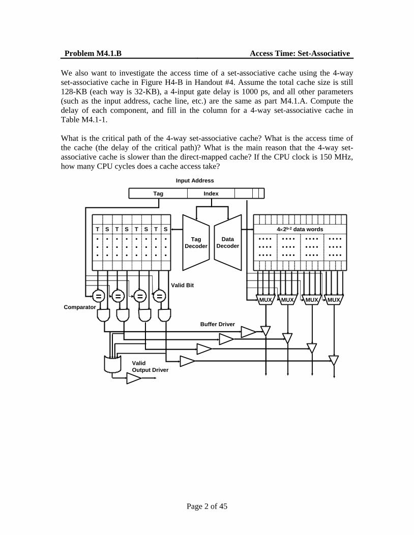
Problem M4.1.B Access Time: Set-Associative
We also want to investigate the access time of a set-associative cache using the 4-way
set-associative cache in Figure H4-B in Handout #4. Assume the total cache size is still
128-KB (each way is 32-KB), a 4-input gate delay is 1000 ps, and all other parameters
(such as the input address, cache line, etc.) are the same as part M4.1.A. Compute the
delay of each component, and fill in the column for a 4-way set-associative cache in
Table M4.1-1.
What is the critical path of the 4-way set-associative cache? What is the access time of
the cache (the delay of the critical path)? What is the main reason that the 4-way set-
associative cache is slower than the direct-mapped cache? If the CPU clock is 150 MHz,
how many CPU cycles does a cache access take?
IndexTag
Input Address
• • • •
• • • •
• • • •
• • • •
• • • •
• • • •
• • • •
• • • •
• • • •
• • • •
• • • •
• • • •
42b-2 data words
•
•
•
S
•
•
•
T
•
•
•
S
•
•
•
T
•
•
•
S
•
•
•
T
•
•
•
S
•
•
•
T
MUX
Tag
Decoder
Data
Decoder
Valid Bit
Valid
Output Driver
=
Buffer Driver
Comparator
MUX MUX MUX= = =
Page 3 of 45
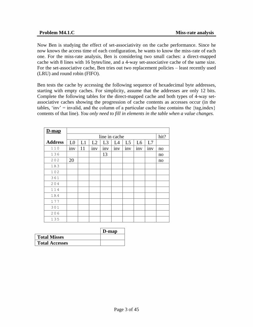
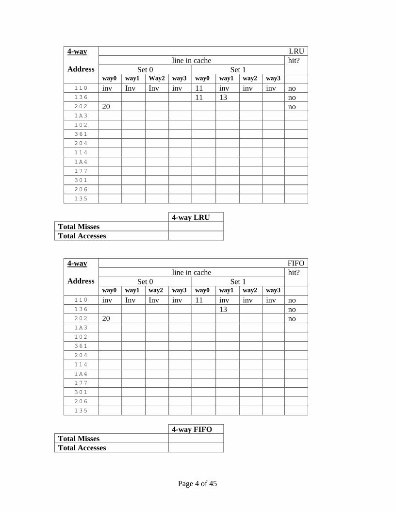
Problem M4.1.C Miss-rate analysis
Now Ben is studying the effect of set-associativity on the cache performance. Since he
now knows the access time of each configuration, he wants to know the miss-rate of each
one. For the miss-rate analysis, Ben is considering two small caches: a direct-mapped
cache with 8 lines with 16 bytes/line, and a 4-way set-associative cache of the same size.
For the set-associative cache, Ben tries out two replacement policies – least recently used
(LRU) and round robin (FIFO).
Ben tests the cache by accessing the following sequence of hexadecimal byte addresses,
starting with empty caches. For simplicity, assume that the addresses are only 12 bits.
Complete the following tables for the direct-mapped cache and both types of 4-way set-
associative caches showing the progression of cache contents as accesses occur (in the
tables, ‘inv’ = invalid, and the column of a particular cache line contains the {tag,index}
contents of that line). You only need to fill in elements in the table when a value changes.
D-map
Address
line in cache hit?
L0 L1 L2 L3 L4 L5 L6 L7 110 inv 11 inv inv inv inv inv inv no 136 13 no 202 20 no 1A3 102 361 204 114 1A4 177 301 206 135
D-map
Total Misses
Total Accesses
Page 4 of 45
4-way
Address
LRU
line in cache hit?
Set 0 Set 1 way0 way1 Way2 way3 way0 way1 way2 way3
110 inv Inv Inv inv 11 inv inv inv no 136 11 13 no 202 20 no 1A3 102 361 204 114 1A4 177 301 206 135
4-way LRU
Total Misses
Total Accesses
4-way
Address
FIFO
line in cache hit?
Set 0 Set 1 way0 way1 way2 way3 way0 way1 way2 way3
110 inv Inv Inv inv 11 inv inv inv no 136 13 no 202 20 no 1A3 102 361 204 114 1A4 177 301 206 135
4-way FIFO
Total Misses
Total Accesses
Page 5 of 45
Problem M4.1.D Average Latency
Assume that the results of the above analysis can represent the average miss-rates of the
direct-mapped and the 4-way LRU 128-KB caches studied in M4.1.A and M4.1.B. What
would be the average memory access latency in CPU cycles for each cache (assume that
a cache miss takes 20 cycles)? Which one is better? For the different replacement policies
for the set-associative cache, which one has a smaller cache miss rate for the address
stream in M4.1.C? Explain why. Is that replacement policy always going to yield better
miss rates? If not, give a counter example using an address stream.
Page 6 of 45
Problem M4.2: Pipelined Cache Access
This problem requires the knowledge of Lecture 6. Please, review it before answering the
following questions. You may also want to take a look at pipeline lectures if you do not
feel comfortable with the topic.
Problem M4.2.A
Ben Bitdiddle is designing a five-stage pipelined MIPS processor with separate 32 KB
direct-mapped primary instruction and data caches. He runs simulations on his
preliminary design, and he discovers that a cache access is on the critical path in his
machine. After remembering that pipelining his processor helped to improve the
machine’s performance, he decides to try applying the same idea to caches. Ben breaks
each cache access into three stages in order to reduce his cycle time. In the first stage the
address is decoded. In the second stage the tag and data memory arrays are accessed; for
cache reads, the data is available by the end of this stage. However, the tag still has to be
checked—this is done in the third stage.
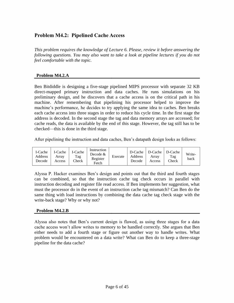
After pipelining the instruction and data caches, Ben’s datapath design looks as follows:
I-Cache
Address
Decode
I-Cache
Array
Access
I-Cache
Tag
Check
Instruction
Decode &
Register
Fetch
Execute
D-Cache
Address
Decode
D-Cache
Array
Access
D-Cache
Tag
Check
Write-
back
Alyssa P. Hacker examines Ben’s design and points out that the third and fourth stages
can be combined, so that the instruction cache tag check occurs in parallel with
instruction decoding and register file read access. If Ben implements her suggestion, what
must the processor do in the event of an instruction cache tag mismatch? Can Ben do the
same thing with load instructions by combining the data cache tag check stage with the
write-back stage? Why or why not?
Problem M4.2.B
Alyssa also notes that Ben’s current design is flawed, as using three stages for a data
cache access won’t allow writes to memory to be handled correctly. She argues that Ben
either needs to add a fourth stage or figure out another way to handle writes. What
problem would be encountered on a data write? What can Ben do to keep a three-stage
pipeline for the data cache?
Page 7 of 45
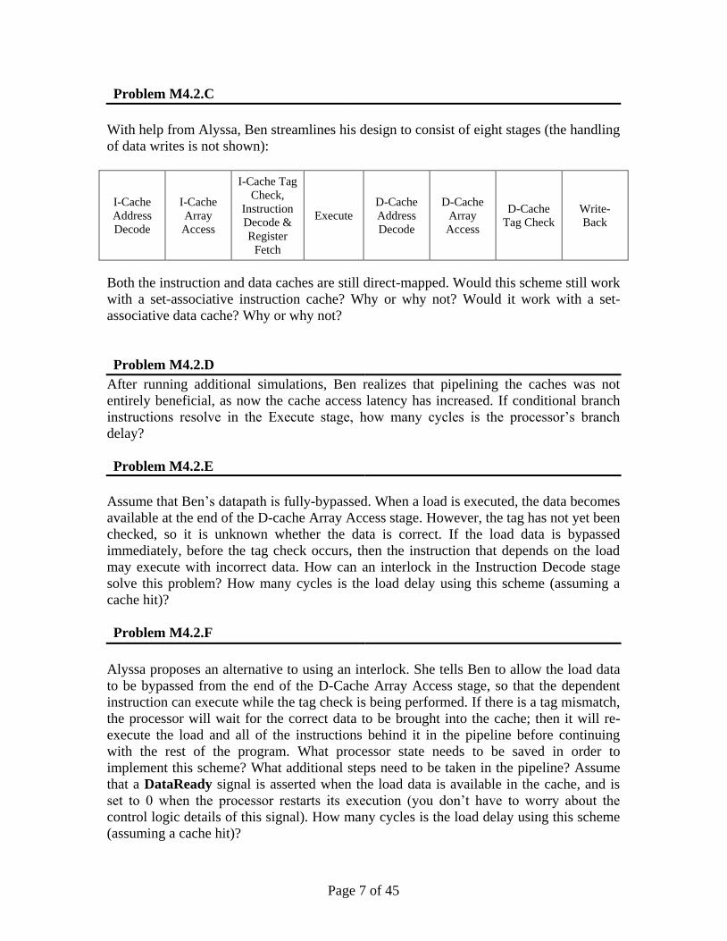
Problem M4.2.C
With help from Alyssa, Ben streamlines his design to consist of eight stages (the handling
of data writes is not shown):
I-Cache
Address
Decode
I-Cache
Array
Access
I-Cache Tag
Check,
Instruction
Decode &
Register
Fetch
Execute
D-Cache
Address
Decode
D-Cache
Array
Access
D-Cache
Tag Check
Write-
Back
Both the instruction and data caches are still direct-mapped. Would this scheme still work
with a set-associative instruction cache? Why or why not? Would it work with a set-
associative data cache? Why or why not?
Problem M4.2.D
After running additional simulations, Ben realizes that pipelining the caches was not
entirely beneficial, as now the cache access latency has increased. If conditional branch
instructions resolve in the Execute stage, how many cycles is the processor’s branch
delay?
Problem M4.2.E
Assume that Ben’s datapath is fully-bypassed. When a load is executed, the data becomes
available at the end of the D-cache Array Access stage. However, the tag has not yet been
checked, so it is unknown whether the data is correct. If the load data is bypassed
immediately, before the tag check occurs, then the instruction that depends on the load
may execute with incorrect data. How can an interlock in the Instruction Decode stage
solve this problem? How many cycles is the load delay using this scheme (assuming a
cache hit)?
Problem M4.2.F
Alyssa proposes an alternative to using an interlock. She tells Ben to allow the load data
to be bypassed from the end of the D-Cache Array Access stage, so that the dependent
instruction can execute while the tag check is being performed. If there is a tag mismatch,
the processor will wait for the correct data to be brought into the cache; then it will re-
execute the load and all of the instructions behind it in the pipeline before continuing
with the rest of the program. What processor state needs to be saved in order to
implement this scheme? What additional steps need to be taken in the pipeline? Assume
that a DataReady signal is asserted when the load data is available in the cache, and is
set to 0 when the processor restarts its execution (you don’t have to worry about the
control logic details of this signal). How many cycles is the load delay using this scheme
(assuming a cache hit)?
Page 8 of 45
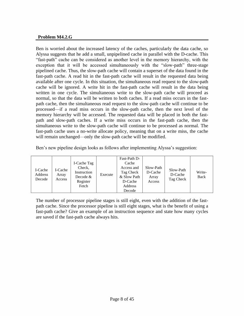
Problem M4.2.G
Ben is worried about the increased latency of the caches, particularly the data cache, so
Alyssa suggests that he add a small, unpipelined cache in parallel with the D-cache. This
“fast-path” cache can be considered as another level in the memory hierarchy, with the
exception that it will be accessed simultaneously with the “slow-path” three-stage
pipelined cache. Thus, the slow-path cache will contain a superset of the data found in the
fast-path cache. A read hit in the fast-path cache will result in the requested data being
available after one cycle. In this situation, the simultaneous read request to the slow-path
cache will be ignored. A write hit in the fast-path cache will result in the data being
written in one cycle. The simultaneous write to the slow-path cache will proceed as
normal, so that the data will be written to both caches. If a read miss occurs in the fast-
path cache, then the simultaneous read request to the slow-path cache will continue to be
processed—if a read miss occurs in the slow-path cache, then the next level of the
memory hierarchy will be accessed. The requested data will be placed in both the fast-
path and slow-path caches. If a write miss occurs in the fast-path cache, then the
simultaneous write to the slow-path cache will continue to be processed as normal. The
fast-path cache uses a no-write allocate policy, meaning that on a write miss, the cache
will remain unchanged—only the slow-path cache will be modified.
Ben’s new pipeline design looks as follows after implementing Alyssa’s suggestion:
I-Cache
Address
Decode
I-Cache
Array
Access
I-Cache Tag
Check,
Instruction
Decode &
Register
Fetch
Execute
Fast-Path D-
Cache
Access and
Tag Check
& Slow Path
D-Cache
Address
Decode
Slow-Path
D-Cache
Array
Access
Slow-Path
D-Cache
Tag Check
Write-
Back
The number of processor pipeline stages is still eight, even with the addition of the fast-
path cache. Since the processor pipeline is still eight stages, what is the benefit of using a
fast-path cache? Give an example of an instruction sequence and state how many cycles
are saved if the fast-path cache always hits.
Page 9 of 45
Problem M4.3: Victim Cache Evaluation
This problem requires the knowledge of Handout #5 (Victim Cache) and Lecture 6.
Please, read these materials before answering the following questions.
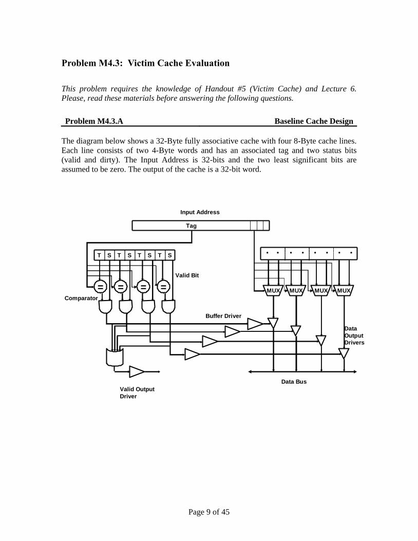
Problem M4.3.A Baseline Cache Design
The diagram below shows a 32-Byte fully associative cache with four 8-Byte cache lines.
Each line consists of two 4-Byte words and has an associated tag and two status bits
(valid and dirty). The Input Address is 32-bits and the two least significant bits are
assumed to be zero. The output of the cache is a 32-bit word.
Tag
Input Address
• •• • • •• •STSTSTST
Valid Bit
=Comparator
= = =
Valid Output
Driver
Buffer Driver
MUX MUX MUX MUX
Data
Output
Drivers
Data Bus
Page 10 of 45
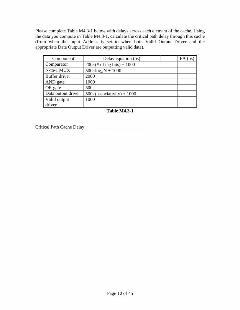
Please complete Table M4.3-1 below with delays across each element of the cache. Using
the data you compute in Table M4.3-1, calculate the critical path delay through this cache
(from when the Input Address is set to when both Valid Output Driver and the
appropriate Data Output Driver are outputting valid data).
Component Delay equation (ps) FA (ps)
Comparator 200(# of tag bits) + 1000
N-to-1 MUX 500log2 N + 1000
Buffer driver 2000
AND gate 1000
OR gate 500
Data output driver 500(associativity) + 1000
Valid output
driver
1000
Table M4.3-1
Critical Path Cache Delay: _______________________
Page 11 of 45
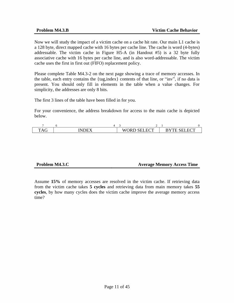
Problem M4.3.B Victim Cache Behavior
Now we will study the impact of a victim cache on a cache hit rate. Our main L1 cache is
a 128 byte, direct mapped cache with 16 bytes per cache line. The cache is word (4-bytes)
addressable. The victim cache in Figure H5-A (in Handout #5) is a 32 byte fully
associative cache with 16 bytes per cache line, and is also word-addressable. The victim
cache uses the first in first out (FIFO) replacement policy.
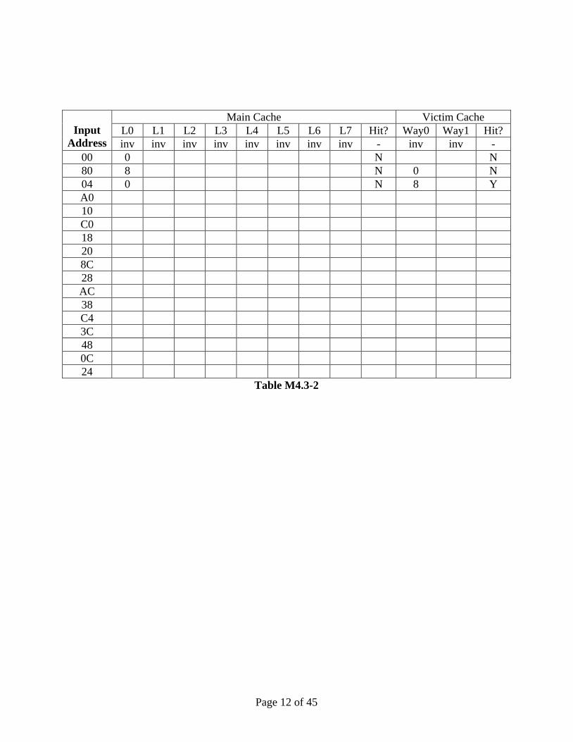
Please complete Table M4.3-2 on the next page showing a trace of memory accesses. In
the table, each entry contains the {tag,index} contents of that line, or “inv”, if no data is
present. You should only fill in elements in the table when a value changes. For
simplicity, the addresses are only 8 bits.
The first 3 lines of the table have been filled in for you.
For your convenience, the address breakdown for access to the main cache is depicted
below.
7 6 4 3 2 1 0
TAG INDEX WORD SELECT BYTE SELECT
Problem M4.3.C Average Memory Access Time
Assume 15% of memory accesses are resolved in the victim cache. If retrieving data
from the victim cache takes 5 cycles and retrieving data from main memory takes 55
cycles, by how many cycles does the victim cache improve the average memory access
time?
Page 12 of 45
Input
Address
Main Cache Victim Cache
L0 L1 L2 L3 L4 L5 L6 L7 Hit? Way0 Way1 Hit?
inv inv inv inv inv inv inv inv - inv inv -
00 0 N N
80 8 N 0 N
04 0 N 8 Y
A0
10
C0
18
20
8C
28
AC
38
C4
3C
48
0C
24
Table M4.3-2
Page 13 of 45
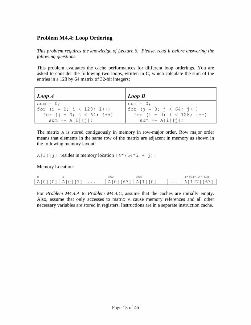
Problem M4.4: Loop Ordering
This problem requires the knowledge of Lecture 6. Please, read it before answering the
following questions.
This problem evaluates the cache performances for different loop orderings. You are
asked to consider the following two loops, written in C, which calculate the sum of the
entries in a 128 by 64 matrix of 32-bit integers:
Loop A Loop B
sum = 0;
for (i = 0; i < 128; i++)
for (j = 0; j < 64; j++)
sum += A[i][j];
sum = 0;
for (j = 0; j < 64; j++)
for (i = 0; i < 128; i++)
sum += A[i][j];
The matrix A is stored contiguously in memory in row-major order. Row major order
means that elements in the same row of the matrix are adjacent in memory as shown in
the following memory layout:
A[i][j] resides in memory location [4*(64*i + j)]
Memory Location:
0 4 252 256 4*(64*127+63)
A[0][0] A[0][1] ... A[0][63] A[1][0] ... A[127][63]
For Problem M4.4.A to Problem M4.4.C, assume that the caches are initially empty.
Also, assume that only accesses to matrix A cause memory references and all other
necessary variables are stored in registers. Instructions are in a separate instruction cache.
Page 14 of 45
Problem M4.4.A
Consider a 4KB direct-mapped data cache with 8-word (32-byte) cache lines.
Calculate the number of cache misses that will occur when running Loop A.
Calculate the number of cache misses that will occur when running Loop B.
The number of cache misses for Loop A:_____________________________
The number of cache misses for Loop B:_____________________________
Problem M4.4.B
Consider a direct-mapped data cache with 8-word (32-byte) cache lines. Calculate the
minimum number of cache lines required for the data cache if Loop A is to run without
any cache misses other than compulsory misses. Calculate the minimum number of cache
lines required for the data cache if Loop B is to run without any cache misses other than
compulsory misses.
Data-cache size required for Loop A: ____________________________ cache line(s)
Data-cache size required for Loop B: ____________________________ cache line(s)
Problem M4.4.C
Consider a 4KB fully-associative data cache with 8-word (32-byte) cache lines. This data
cache uses a first-in/first-out (FIFO) replacement policy.
Calculate the number of cache misses that will occur when running Loop A.
Calculate the number of cache misses that will occur when running Loop B.
The number of cache misses for Loop A:_____________________________
The number of cache misses for Loop B:_____________________________
Page 15 of 45
Problem M4.5: Cache Parameters
For each of the following statements about making a change to a cache design, circle
True or False and provide a one sentence explanation of your choice. Assume all cache
parameters (capacity, associativity, line size) remain fixed except for the single change
described in each question. Please provide a one sentence explanation of your answer.
Problem M4.5.A
Doubling the line size halves the number of tags in the cache
True / False
Problem M4.5.B
Doubling the associativity doubles the number of tags in the cache.
True / False
Problem M4.5.C
Doubling cache capacity of a direct-mapped cache usually reduces conflict misses.
True / False
Problem M4.5.D
Doubling cache capacity of a direct-mapped cache usually reduces compulsory misses.
True / False
Problem M4.5.E
Doubling the line size usually reduces compulsory misses.
True / False
Page 16 of 45
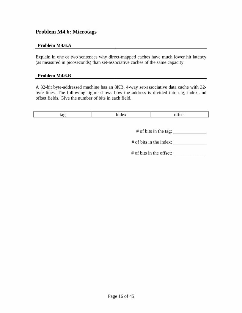
Problem M4.6: Microtags
Problem M4.6.A
Explain in one or two sentences why direct-mapped caches have much lower hit latency
(as measured in picoseconds) than set-associative caches of the same capacity.
Problem M4.6.B
A 32-bit byte-addressed machine has an 8KB, 4-way set-associative data cache with 32-
byte lines. The following figure shows how the address is divided into tag, index and
offset fields. Give the number of bits in each field.
tag Index offset
# of bits in the tag: ______________
# of bits in the index: ______________
# of bits in the offset: ______________
Page 17 of 45
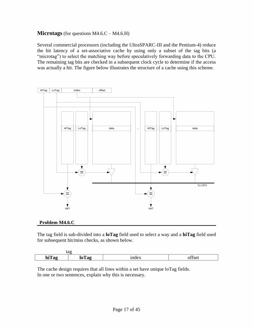
Microtags (for questions M4.6.C – M4.6.H)
Several commercial processors (including the UltraSPARC-III and the Pentium-4) reduce
the hit latency of a set-associative cache by using only a subset of the tag bits (a
“microtag”) to select the matching way before speculatively forwarding data to the CPU.
The remaining tag bits are checked in a subsequent clock cycle to determine if the access
was actually a hit. The figure below illustrates the structure of a cache using this scheme.
HiTag LoTag data
HiTag LoTag
=
Index offset
HiTag LoTag data
=
...
To CPU
==
Hit?Hit?
Problem M4.6.C
The tag field is sub-divided into a loTag field used to select a way and a hiTag field used
for subsequent hit/miss checks, as shown below.
tag
hiTag loTag index offset
The cache design requires that all lines within a set have unique loTag fields.
In one or two sentences, explain why this is necessary.
Page 18 of 45
Problem M4.6.D
If the loTag field is exactly two bits long, will the cache have greater, fewer, or an equal
number of conflict misses as a direct-mapped cache of the same capacity? State any
assumptions made about replacement policy.
Problem M4.6.E
If the loTag field is greater than two bits long, are there any additional constraints on
replacement policy beyond those in a conventional 4-way set-associative cache?
Problem M4.6.F
Does this scheme reduce the time required to complete a write to the cache? Explain in
one or two sentences.
Problem M4.6.G
In practice, microtags hold virtual address bits to remove address translation from the
critical path, while the full tag check is performed on translated physical addresses. If the
loTag bits can only hold untranslated bits of the virtual address, what is the largest
number of loTag bits possible if the machine has a 16KB virtual memory page size?
(Assume 8KB 4-way set-associative cache as in Question M4.6.B)
Problem M4.6.H
Describe how microtags can be made much larger, to also include virtual address bits
subject to address translation. Your design should not require address translation before
speculatively forwarding data to the CPU. Your explanation should describe the
replacement policy and any additional state the machine must maintain.
Page 19 of 45
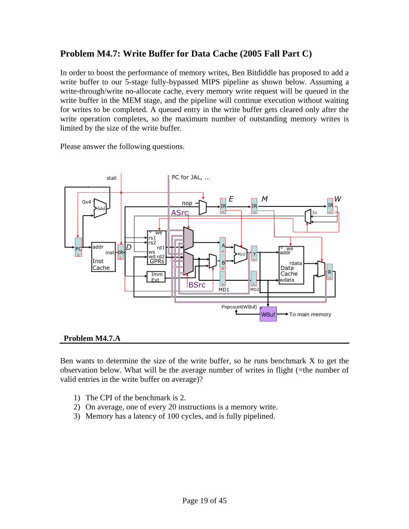
Problem M4.7: Write Buffer for Data Cache (2005 Fall Part C)
In order to boost the performance of memory writes, Ben Bitdiddle has proposed to add a
write buffer to our 5-stage fully-bypassed MIPS pipeline as shown below. Assuming a
write-through/write no-allocate cache, every memory write request will be queued in the
write buffer in the MEM stage, and the pipeline will continue execution without waiting
for writes to be completed. A queued entry in the write buffer gets cleared only after the
write operation completes, so the maximum number of outstanding memory writes is
limited by the size of the write buffer.
Please answer the following questions.
ASrcIRIR IR
PCA
B
Y
R
MD1 MD2
addrinst
InstCache
0x4
Add
IR ALU
ImmExt
rd1
GPRs
rs1rs2
wswd rd2
we
wdata
addr
wdata
rdataData Cache
we
31
nop
stall
D
E M W
PC for JAL, ...
BSrc
WBuf To main memory
Popcount(WBuf)
Problem M4.7.A
Ben wants to determine the size of the write buffer, so he runs benchmark X to get the
observation below. What will be the average number of writes in flight (=the number of
valid entries in the write buffer on average)?
1) The CPI of the benchmark is 2.
2) On average, one of every 20 instructions is a memory write.
3) Memory has a latency of 100 cycles, and is fully pipelined.
Page 20 of 45
Problem M4.7.B
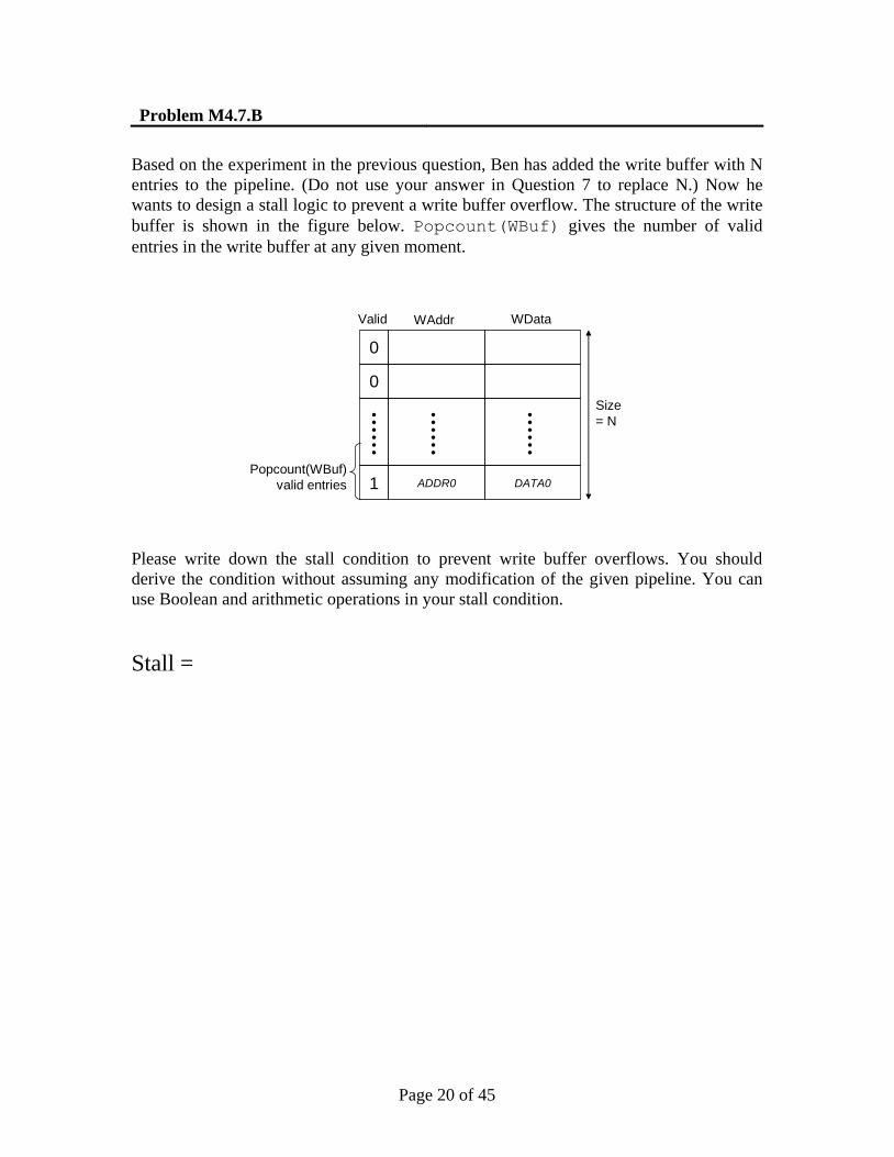
Based on the experiment in the previous question, Ben has added the write buffer with N
entries to the pipeline. (Do not use your answer in Question 7 to replace N.) Now he
wants to design a stall logic to prevent a write buffer overflow. The structure of the write
buffer is shown in the figure below. Popcount(WBuf) gives the number of valid
entries in the write buffer at any given moment.
ADDR0 DATA0
WAddr WData
0
0
1
Valid
Size
= N
Popcount(WBuf)
valid entries
Please write down the stall condition to prevent write buffer overflows. You should
derive the condition without assuming any modification of the given pipeline. You can
use Boolean and arithmetic operations in your stall condition.
Stall =
Page 21 of 45
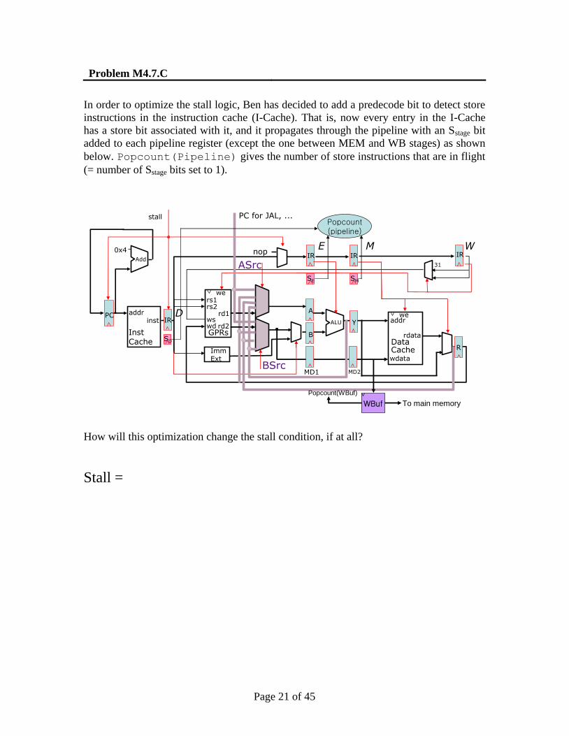
Problem M4.7.C
In order to optimize the stall logic, Ben has decided to add a predecode bit to detect store
instructions in the instruction cache (I-Cache). That is, now every entry in the I-Cache
has a store bit associated with it, and it propagates through the pipeline with an Sstage bit
added to each pipeline register (except the one between MEM and WB stages) as shown
below. Popcount(Pipeline) gives the number of store instructions that are in flight
(= number of Sstage bits set to 1).
ASrcIRIR IR
PCA
B
Y
R
MD1 MD2
addrinst
InstCache
0x4
Add
IR ALU
ImmExt
rd1
GPRs
rs1rs2
wswd rd2
we
wdata
addr
wdata
rdataData Cache
we
31
nop
stall
D
E M W
PC for JAL, ...
BSrc
WBuf
SD
SE SM
Popcount(pipeline)
To main memory
Popcount(WBuf)
How will this optimization change the stall condition, if at all?
Stall =
Page 22 of 45
Problem M5.1: Virtual Memory Bits
This problem requires the knowledge of Handout #6 (Virtual Memory Implementation)
and Lecture 7 and 8. Please, read these materials before answering the following
questions.
In this problem we consider simple virtual memory enhancements.
Problem M5.1.A
Whenever a TLB entry is replaced we write the entire entry back to the page table. Ben
thinks this is a waste of memory bandwidth. He thinks only a few of the bits need to be
written back. For each of the bits explain why or why not they need to be written back to
the page table.
With this in mind, we will see how we can minimize the number of bits we actually need
in each TLB entry throughout the rest of the problem.
Problem M5.1.B
Ben does not like the TLB design. He thinks the TLB Entry Valid bit should be dropped
and the kernel software should be changed to ensure that all TLB entries are always valid.
Is this a good idea? Explain the advantages and disadvantages of such a design.
Problem M5.1.C
Alyssa got wind of Ben’s idea and suggests a different scheme to eliminate one of the
valid bits. She thinks the page table entry valid and TLB Entry Valid bits can be
combined into a single bit.
On a refill this combined valid bit will take the value that the page table entry valid bit
had. A TLB entry is invalidated by writing it back to the page table and setting the
combined valid bit in the TLB entry to invalid.
How does the kernel software need to change to make such a scheme work? How do the
exceptions that the TLB produces change?
Page 23 of 45
Problem M5.1.D
Now, Bud Jet jumps into the game. He wants to keep the TLB Entry Valid bit. However,
there is no way he is going to have two valid bits in each TLB entry (one for the TLB
entry one for the page table entry). Thus, he decides to drop the page table entry valid bit
from the TLB entry.
How does the kernel software need to change to make this work well? How do the
exceptions that the TLB produces change?
Problem M5.1.E
Compare your answers to Problem M5.1.C and M5.1.D. What scheme will lead to better
performance?
Problem M5.1.F
How about the R bit? Can we remove them from the TLB entry without significantly
impacting performance? Explain briefly.
Problem M5.1.G
The processor has a kernel (supervisor) mode bit. Whenever kernel software executes the
bit is set. When user code executes the bit is not set. Parts of the user’s virtual address
space are only accessible to the kernel. The supervisor bit in the page table is used to
protect this region—an exception is raised if the user tries to access a page that has the
supervisor bit set.
Bud Jet is on a roll and he decides to eliminate the supervisor bit from each TLB entry.
Explain how the kernel software needs to change so that we still have the protection
mechanism and the kernel can still access these pages through the virtual memory
system.
Problem M5.1.H
Alyssa P. Hacker thinks Ben and Bud are being a little picky about these bits, but has
devised a scheme where the TLB entry does not need the M bit or the U bit. It works as
follows. If a TLB miss occurs due to a load, then the page table entry is read from
memory and placed in the TLB. However, in this case the W bit will always be set to 0.
Provide the details of how the rest of the scheme works (what happens during a store,
when do the entries need to be written back to memory, when are the U and M bits
modified in the page table, etc.).
Page 24 of 45
Problem M5.2: Page Size and TLBs (2005 Fall Part D)
This problem requires the knowledge of Handout #6 (Virtual Memory Implementation)
and Lecture 8. Please, read these materials before answering the following questions.
Assume that we use a hierarchical page table described in Handout #6.
The processor has a data TLB with 64 entries, and each entry can map either a 4KB page
or a 4MB page. After a TLB miss, a hardware engine walks the page table to reload the
TLB. The TLB uses a first-in/first-out (FIFO) replacement policy.
We will evaluate the memory usage and execution of the following program which adds
the elements from two 1MB arrays and stores the results in a third 1MB array (note that,
1MB = 1,048,576 Bytes):
We assume the A, B, and C arrays are allocated in a contiguous 3MB region of physical
memory. We will consider two possible virtual memory mappings:
4KB: the arrays are mapped using 768 4KB pages (each array uses 256 pages).
4MB: the arrays are mapped using a single 4MB page.
For the following questions, assume that the above program is the only process in the
system, and ignore any instruction memory or operating system overheads. Assume that
the arrays are aligned in memory to minimize the number of page table entries needed.
byte A[1048576]; // 1MB array
byte B[1048576]; // 1MB array
byte C[1048576]; // 1MB array
for(int i=0; i<1048576; i++)
C[i] = A[i] + B[i];
Page 25 of 45
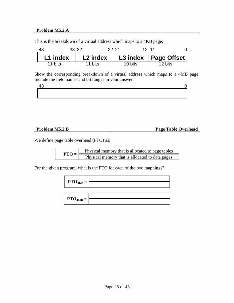
Problem M5.2.A
This is the breakdown of a virtual address which maps to a 4KB page:
Show the corresponding breakdown of a virtual address which maps to a 4MB page.
Include the field names and bit ranges in your answer.
Problem M5.2.B Page Table Overhead
We define page table overhead (PTO) as:
PTO = Physical memory that is allocated to page tables
Physical memory that is allocated to data pages
For the given program, what is the PTO for each of the two mappings?
PTO4KB =
PTO4MB =
L1 index
33 43
L2 index
22 32
L3 index
12 21
Page Offset
0 11
11 bits 11 bits 10 bits 12 bits
43 0
Page 26 of 45
Problem M5.2.C Page Fragmentation Overhead
We define page fragmentation overhead (PFO) as:
PFO = Physical memory that is allocated to data pages but is never accessed
Physical memory that is allocated to data pages and is accessed
For the given program, what is the PFO for each of the two mappings?
PFO4KB =
PFO4MB =
Problem M5.2.D
Consider the execution of the given program, assuming that the data TLB is initially
empty. For each of the two mappings, how many TLB misses occur, and how many page
table memory references are required per miss to reload the TLB?
Data TLB misses
Page table memory
references (per miss)
4KB:
4MB:
Problem M5.2.E
Which of the following is the best estimate for how much longer the program takes to
execute with the 4KB page mapping compared to the 4MB page mapping?
Circle one choice and briefly explain your answer (about one sentence).
1.01 10 1,000 1,000,000
Page 27 of 45
Problem M5.3: Page Size and TLBs
This problem requires the knowledge of Handout #6 (Virtual Memory Implementation)
and Lecture 8. Please, read these materials before answering the following questions.
The configuration of the hierarchical page table in this problem is similar to the one in
Handout #6, but we modify two parameters: 1) this problem evaluates a virtual memory
system with two page sizes, 4KB and 1MB (instead of 4 MB), and 2) all PTEs are 16
Bytes (instead of 8 Bytes). The following figure summarizes the page table structure and
indicates the sizes of the page tables and data pages (not drawn to scale):
The processor has a data TLB with 64 entries, and each entry can map either a 4KB page
or a 1MB page. After a TLB miss, a hardware engine walks the page table to reload the
TLB. The TLB uses a first-in/first-out (FIFO) replacement policy.
We will evaluate the execution of the following program which adds the elements from
two 1MB arrays and stores the results in a third 1MB array (note that, 1MB = 1,048,576
Bytes, the starting address of the arrays are given below):
Assume that the above program is the only process in the system, and ignore any
instruction memory or operating system overheads. The data TLB is initially empty.
L1 Table (4096 PTEs, 64KB)
L2 Table (4096 PTEs, 64KB)
L3 Table (256 PTEs, 4KB)
Data Page (4KB)
Data Page (1MB)
Root ptr. (processor
register)
byte A[1048576]; // 1MB array 0x00001000000
byte B[1048576]; // 1MB array 0x00001100000
byte C[1048576]; // 1MB array 0x00001200000
for(int i=0; i<1048576; i++)
C[i] = A[i] + B[i];
Page 28 of 45
Problem M5.3.A
Consider the execution of the program. There is no cache and each memory lookup has
100 cycle latency.
If all data pages are 4KB, compute the ratio of cycles for address translation to cycles for
data access.
If all data pages are 1MB, compute the ratio of cycles for address translation to cycles for
data access.
Problem M5.3.B
For this question, assume that in addition, we have a PTE cache with one cycle latency. A
PTE cache contains page table entries. If this PTE cache has unlimited capacity, compute
the ratio of cycles for address translation to cycles for data access for the 4KB data page
case.
Problem M5.3.C
With the use of a PTE cache, is there any benefit to caching L3 PTE entries? Explain.
Problem M5.3.D
What is the minimum capacity (number of entries) needed in the PTE cache to get the
same performance as an unlimited PTE cache? (Assume that the PTE cache does not
cache L3 PTE entries and all data pages are 4KB)
Problem M5.3.E
Instead of a PTE cache, we allow the data cache to cache data as well as PTEs. The data
cache is a 4KB direct-mapped with 16 byte lines. Compute the ratio of cycles for address
translation to cycles for data access for the 4KB data page case.
Page 29 of 45
Problem M5.4: 64-bit Virtual Memory
This problem examines page tables in the context of processors with 64-bit addressing.
Problem M5.4.A Single level page tables
For a computer with 64-bit virtual addresses, how large is the page table if only a single-
level page table is used? Assume that each page is 4KB, that each page table entry is 8
bytes, and that the processor is byte-addressable.
Problem M5.4.B Let’s be practical
Many current implementations of 64-bit ISAs implement only part of the large virtual
address space. One way to do this is to segment the virtual address space into three parts
as shown below: one used for stack, one used for code and heap data, and the third one
unused.
A special circuit is used to detect whether the top eight bits of an address are all zeros or
all ones before the address is sent to the virtual memory system. If they are not all equal,
an invalid virtual memory address trap is raised. This scheme in effect removes the top
seven bits from the virtual memory address, but retains a memory layout that will be
compatible with future designs that implement a larger virtual address space.
The MIPS R10000 does something similar. Because a 64-bit address is unnecessarily
large, only the low 44 address bits are translated. This also reduces the cost of TLB and
cache tag arrays. The high two virtual address bits (bits 63:62) select between user,
supervisor, and kernel address spaces. The intermediate address bits (61:44) must either
be all zeros or all ones, depending on the address region.
How large is a single-level page table that would support MIPS R10000 addresses?
Assume that each page is 4KB, that each page table entry is 8 bytes, and that the
processor is byte-addressable.
Reserved for Code and Heap
Reserved for Stack
0xFFFFFFFFFFFFFFFF
0xFF00000000000000
0x00FFFFFFFFFFFFFF
0x0000000000000000
Unused
Page 30 of 45
Problem M5.4.C Page table overhead
A three-level hierarchical page table can be used to reduce the page table size. Suppose
we break up the 44-bit virtual address (VA) as follows:
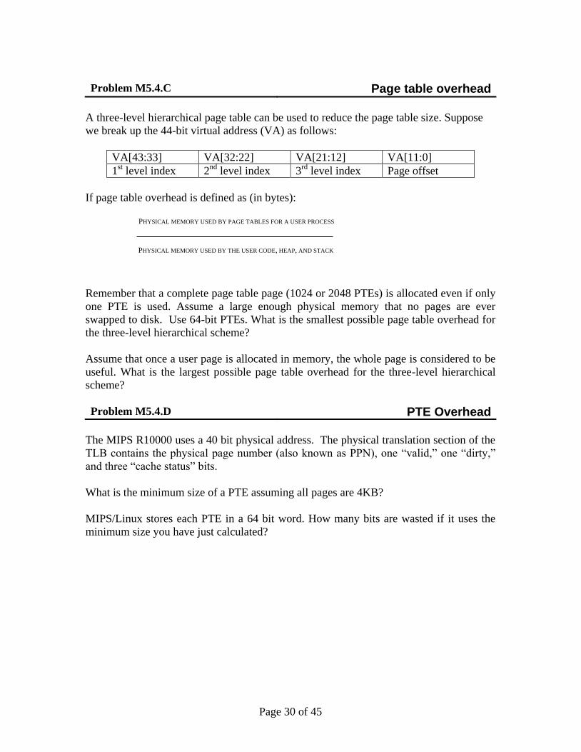
VA[43:33] VA[32:22] VA[21:12] VA[11:0]
1st level index 2
nd level index 3
rd level index Page offset
If page table overhead is defined as (in bytes):
PHYSICAL MEMORY USED BY PAGE TABLES FOR A USER PROCESS
PHYSICAL MEMORY USED BY THE USER CODE, HEAP, AND STACK
Remember that a complete page table page (1024 or 2048 PTEs) is allocated even if only
one PTE is used. Assume a large enough physical memory that no pages are ever
swapped to disk. Use 64-bit PTEs. What is the smallest possible page table overhead for
the three-level hierarchical scheme?
Assume that once a user page is allocated in memory, the whole page is considered to be
useful. What is the largest possible page table overhead for the three-level hierarchical
scheme?
Problem M5.4.D PTE Overhead
The MIPS R10000 uses a 40 bit physical address. The physical translation section of the
TLB contains the physical page number (also known as PPN), one “valid,” one “dirty,”
and three “cache status” bits.
What is the minimum size of a PTE assuming all pages are 4KB?
MIPS/Linux stores each PTE in a 64 bit word. How many bits are wasted if it uses the
minimum size you have just calculated?
Page 31 of 45
Problem M5.4.E Page table implementation
The following comment is from the source code of MIPS/Linux and, despite its cryptic
terminology, describes a three-level page table.
/*
* Each address space has 2 4K pages as its page directory, giving 1024
* 8 byte pointers to pmd tables. Each pmd table is a pair of 4K pages,
* giving 1024 8 byte pointers to page tables. Each (3rd level) page
* table is a single 4K page, giving 512 8 byte ptes.
*
* /
Assuming 4K pages, how long is each index?
Index Length (bits)
Top-level (“page directory”)
2nd
-level
3rd
-level
Problem M5.4.F Variable Page Sizes
A TLB may have a page mask field that allows an entry to map a page size of any power
of four between 4KB and 16MB. The page mask specifies which bits of the virtual
address represent the page offset (and should therefore not be included in translation).
What are the maximum and minimum reach of a 64-entry TLB using such a mask? The
R10000 actually doubles this reach with little overhead by having each TLB entry map
two physical pages, but don’t worry about that here.
Problem M5.4.G Virtual Memory and Caches
Ben Bitdiddle is designing a 4-way set associative cache that is virtually indexed and
virtually tagged. He realizes that such a cache suffers from a homonym aliasing problem.
The homonym problem happens when two processes use the same virtual address to
access different physical locations. Ben asks Alyssa P. Hacker for help with solving this
problem. She suggests that Ben should add a PID (Process ID) to the virtual tag. Does
this solve the homonym problem?
Another problem with virtually indexed and virtually tagged caches is called synonym
problem. Synonym problem happens when distinct virtual addresses refer to the same
physical location. Does Alyssa’s idea solve this problem?
Page 32 of 45
Ben thinks that a different way of solving synonym and homonym problems is to have a
direct mapped cache, rather than a set associative cache. Is he right?
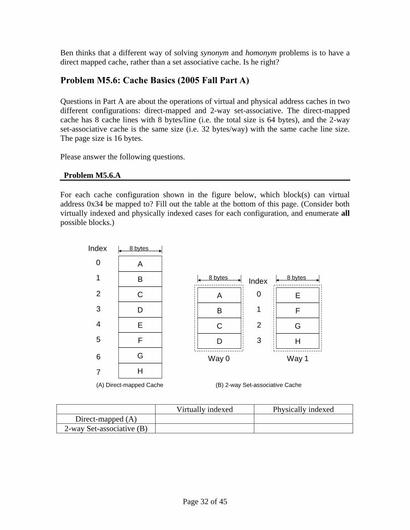
Problem M5.6: Cache Basics (2005 Fall Part A)
Questions in Part A are about the operations of virtual and physical address caches in two
different configurations: direct-mapped and 2-way set-associative. The direct-mapped
cache has 8 cache lines with 8 bytes/line (i.e. the total size is 64 bytes), and the 2-way
set-associative cache is the same size (i.e. 32 bytes/way) with the same cache line size.
The page size is 16 bytes.
Please answer the following questions.
Problem M5.6.A
For each cache configuration shown in the figure below, which block(s) can virtual
address 0x34 be mapped to? Fill out the table at the bottom of this page. (Consider both
virtually indexed and physically indexed cases for each configuration, and enumerate all
possible blocks.)
A
B
C
D
E
F
G
H
Index
0
1
2
3
4
5
6
7
8 bytes
A
B
C
D
8 bytes
E
F
G
H
8 bytes
Way 0 Way 1
Index
0
1
2
3
(A) Direct-mapped Cache (B) 2-way Set-associative Cache
Virtually indexed Physically indexed
Direct-mapped (A)
2-way Set-associative (B)
Page 33 of 45
Problem M5.6.B
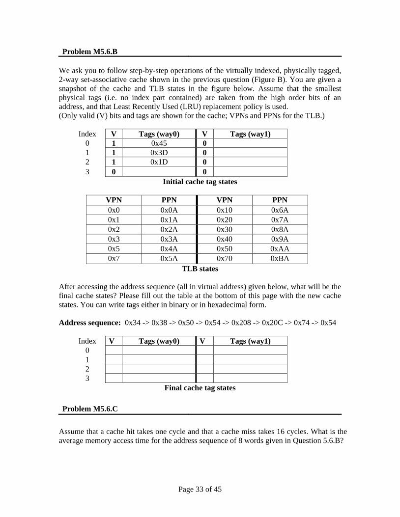
We ask you to follow step-by-step operations of the virtually indexed, physically tagged,
2-way set-associative cache shown in the previous question (Figure B). You are given a
snapshot of the cache and TLB states in the figure below. Assume that the smallest
physical tags (i.e. no index part contained) are taken from the high order bits of an
address, and that Least Recently Used (LRU) replacement policy is used.
(Only valid (V) bits and tags are shown for the cache; VPNs and PPNs for the TLB.)
Index V Tags (way0) V Tags (way1)
0 1 0x45 0
1 1 0x3D 0
2 1 0x1D 0
3 0 0
Initial cache tag states
VPN PPN VPN PPN
0x0 0x0A 0x10 0x6A
0x1 0x1A 0x20 0x7A
0x2 0x2A 0x30 0x8A
0x3 0x3A 0x40 0x9A
0x5 0x4A 0x50 0xAA
0x7 0x5A 0x70 0xBA
TLB states
After accessing the address sequence (all in virtual address) given below, what will be the
final cache states? Please fill out the table at the bottom of this page with the new cache
states. You can write tags either in binary or in hexadecimal form.
Address sequence: 0x34 -> 0x38 -> 0x50 -> 0x54 -> 0x208 -> 0x20C -> 0x74 -> 0x54
Index V Tags (way0) V Tags (way1)
0
1
2
3
Final cache tag states
Problem M5.6.C
Assume that a cache hit takes one cycle and that a cache miss takes 16 cycles. What is the
average memory access time for the address sequence of 8 words given in Question 5.6.B?
Page 34 of 45
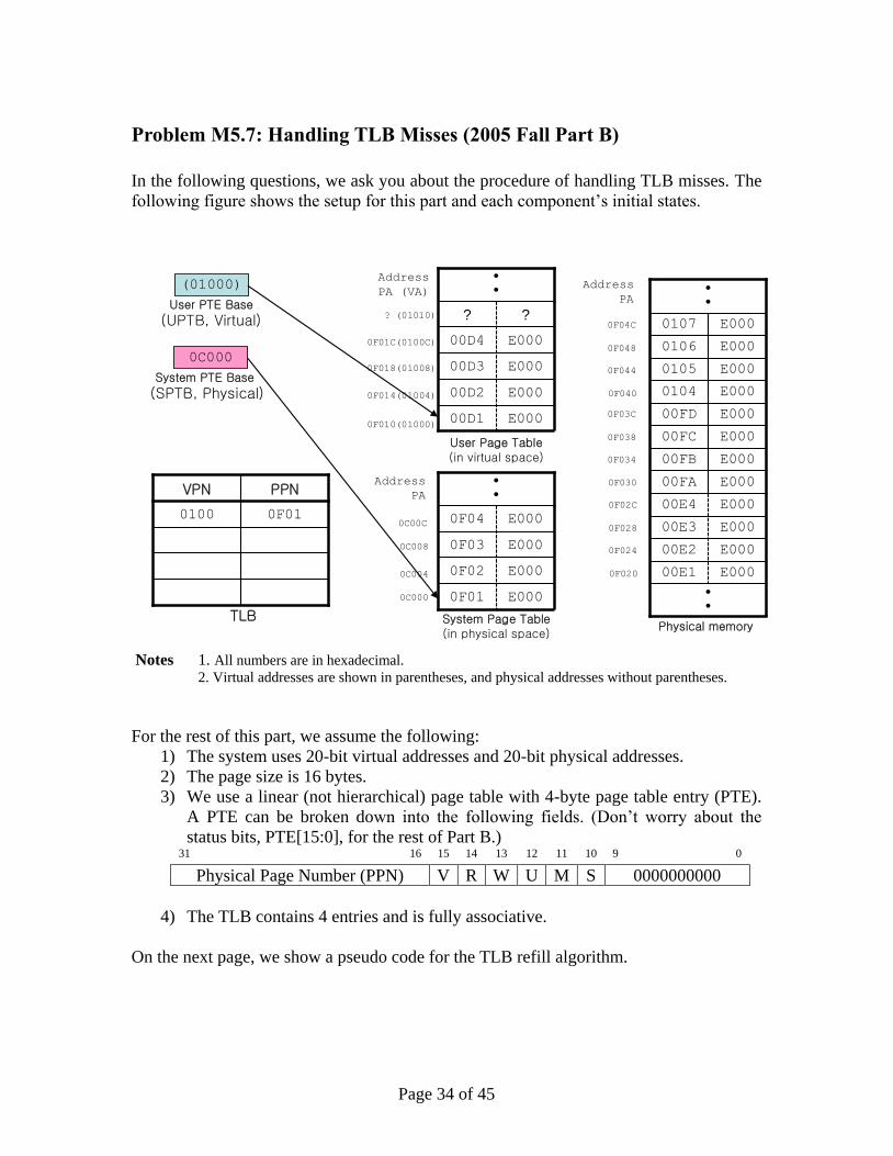
Problem M5.7: Handling TLB Misses (2005 Fall Part B)
In the following questions, we ask you about the procedure of handling TLB misses. The
following figure shows the setup for this part and each component’s initial states.
(01000)
User PTE Base
(UPTB, Virtual)
0C000
System PTE Base
(SPTB, Physical)
??
E00000D1
E00000D2
E00000D3
E00000D4
••
0F010(01000)
0F014(01004)
0F018(01008)
0F01C(0100C)
? (01010)
E0000F01
E0000F02
E0000F03
E0000F04
••
0C000
0C004
0C008
0C00C
User Page Table (in virtual space)
System Page Table (in physical space)
••
E0000107
E0000106
E0000105
E0000104
E000
E000
E000
E00000FD
00FC
00FB
00FA
E00000E1
••
E00000E2
E00000E3
E00000E4
0F020
0F024
0F028
0F02C
0F030
0F034
0F038
0F03C
0F040
0F044
0F048
0F04C
Physical memory
Address
PA (VA)
Address
PA
Address
PA
0F010100
PPNVPN
TLB
Notes 1. All numbers are in hexadecimal.
2. Virtual addresses are shown in parentheses, and physical addresses without parentheses.
For the rest of this part, we assume the following:
1) The system uses 20-bit virtual addresses and 20-bit physical addresses.
2) The page size is 16 bytes.
3) We use a linear (not hierarchical) page table with 4-byte page table entry (PTE).
A PTE can be broken down into the following fields. (Don’t worry about the
status bits, PTE[15:0], for the rest of Part B.) 31 16 15 14 13 12 11 10 9 0
Physical Page Number (PPN) V R W U M S 0000000000
4) The TLB contains 4 entries and is fully associative.
On the next page, we show a pseudo code for the TLB refill algorithm.
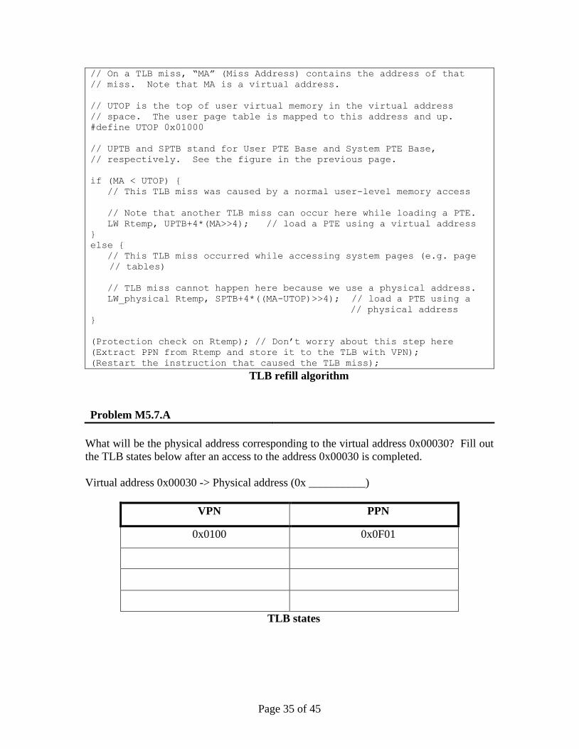
Page 35 of 45
// On a TLB miss, “MA” (Miss Address) contains the address of that
// miss. Note that MA is a virtual address.
// UTOP is the top of user virtual memory in the virtual address
// space. The user page table is mapped to this address and up.
#define UTOP 0x01000
// UPTB and SPTB stand for User PTE Base and System PTE Base,
// respectively. See the figure in the previous page.
if (MA < UTOP) {
// This TLB miss was caused by a normal user-level memory access
// Note that another TLB miss can occur here while loading a PTE.
LW Rtemp, UPTB+4*(MA>>4); // load a PTE using a virtual address
}
else {
// This TLB miss occurred while accessing system pages (e.g. page
// tables)
// TLB miss cannot happen here because we use a physical address.
LW_physical Rtemp, SPTB+4*((MA-UTOP)>>4); // load a PTE using a
// physical address
}
(Protection check on Rtemp); // Don’t worry about this step here
(Extract PPN from Rtemp and store it to the TLB with VPN);
(Restart the instruction that caused the TLB miss);
TLB refill algorithm
Problem M5.7.A
What will be the physical address corresponding to the virtual address 0x00030? Fill out
the TLB states below after an access to the address 0x00030 is completed.
Virtual address 0x00030 -> Physical address (0x __________)
VPN PPN
0x0100 0x0F01
TLB states
Page 36 of 45
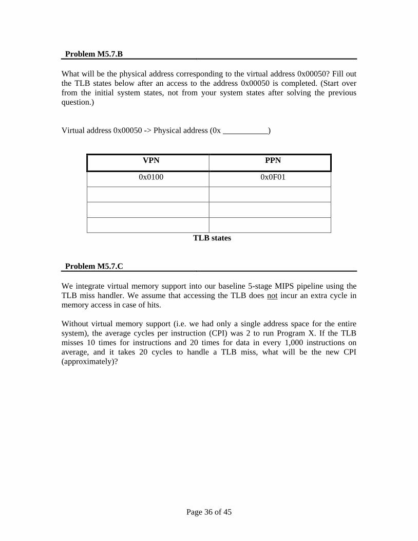
Problem M5.7.B
What will be the physical address corresponding to the virtual address 0x00050? Fill out
the TLB states below after an access to the address 0x00050 is completed. (Start over
from the initial system states, not from your system states after solving the previous
question.)
Virtual address 0x00050 -> Physical address (0x ___________)
VPN PPN
0x0100 0x0F01
TLB states
Problem M5.7.C
We integrate virtual memory support into our baseline 5-stage MIPS pipeline using the
TLB miss handler. We assume that accessing the TLB does not incur an extra cycle in
memory access in case of hits.
Without virtual memory support (i.e. we had only a single address space for the entire
system), the average cycles per instruction (CPI) was 2 to run Program X. If the TLB
misses 10 times for instructions and 20 times for data in every 1,000 instructions on
average, and it takes 20 cycles to handle a TLB miss, what will be the new CPI
(approximately)?
Page 37 of 45
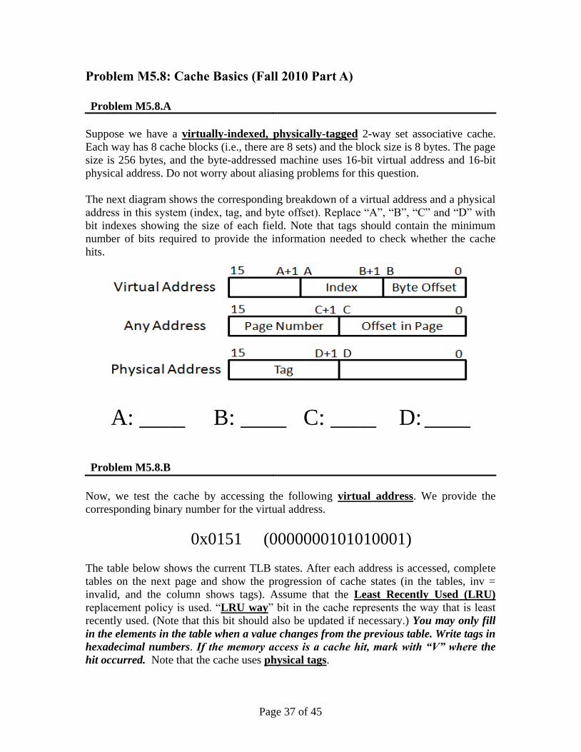
Problem M5.8: Cache Basics (Fall 2010 Part A)
Problem M5.8.A
Suppose we have a virtually-indexed, physically-tagged 2-way set associative cache.
Each way has 8 cache blocks (i.e., there are 8 sets) and the block size is 8 bytes. The page
size is 256 bytes, and the byte-addressed machine uses 16-bit virtual address and 16-bit
physical address. Do not worry about aliasing problems for this question.
The next diagram shows the corresponding breakdown of a virtual address and a physical
address in this system (index, tag, and byte offset). Replace “A”, “B”, “C” and “D” with
bit indexes showing the size of each field. Note that tags should contain the minimum
number of bits required to provide the information needed to check whether the cache
hits.
A: ____ B: ____ C: ____ D: ____
Problem M5.8.B
Now, we test the cache by accessing the following virtual address. We provide the
corresponding binary number for the virtual address.
0x0151 (0000000101010001)
The table below shows the current TLB states. After each address is accessed, complete
tables on the next page and show the progression of cache states (in the tables, inv =
invalid, and the column shows tags). Assume that the Least Recently Used (LRU)
replacement policy is used. “LRU way” bit in the cache represents the way that is least
recently used. (Note that this bit should also be updated if necessary.) You may only fill
in the elements in the table when a value changes from the previous table. Write tags in
hexadecimal numbers. If the memory access is a cache hit, mark with “V” where the
hit occurred. Note that the cache uses physical tags.
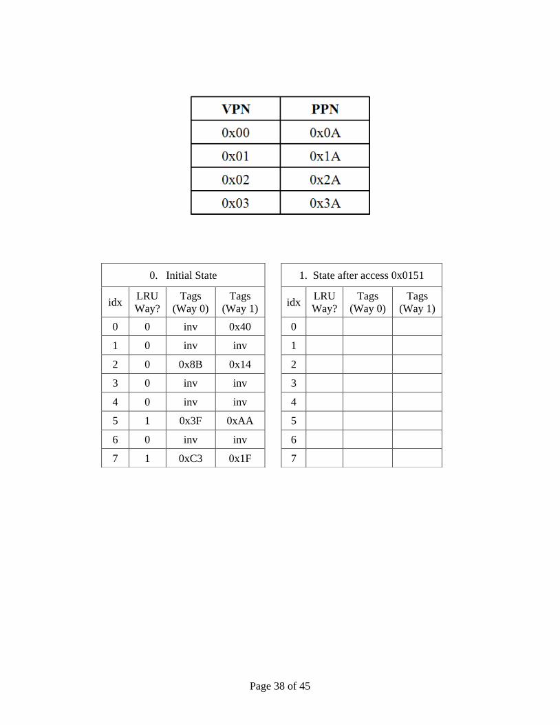
Page 38 of 45
0. Initial State
1. State after access 0x0151
idx
LRU
Way?
Tags
(Way 0)
Tags
(Way 1)
idx LRU
Way?
Tags
(Way 0)
Tags
(Way 1)
0 0 inv 0x40
0
1 0 inv inv
1
2 0 0x8B 0x14
2
3 0 inv inv
3
4 0 inv inv
4
5 1 0x3F 0xAA
5
6 0 inv inv
6
7 1 0xC3 0x1F
7
Page 39 of 45
Problem M5.8.C
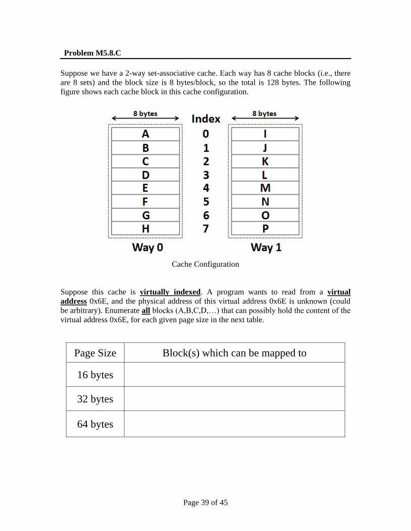
Suppose we have a 2-way set-associative cache. Each way has 8 cache blocks (i.e., there
are 8 sets) and the block size is 8 bytes/block, so the total is 128 bytes. The following
figure shows each cache block in this cache configuration.
Cache Configuration
Suppose this cache is virtually indexed. A program wants to read from a virtual
address 0x6E, and the physical address of this virtual address 0x6E is unknown (could
be arbitrary). Enumerate all blocks (A,B,C,D,…) that can possibly hold the content of the
virtual address 0x6E, for each given page size in the next table.
Page Size Block(s) which can be mapped to
16 bytes
32 bytes
64 bytes
Page 40 of 45
Problem M5.8.D
Now, suppose the cache is physically indexed. A program wants to read from the same
virtual address 0x6E, and the physical address of this virtual address 0x6E is unknown
(could be arbitrary). Enumerate all blocks (A,B,C,D,…) that can possibly hold the
content of the virtual address 0x6E, for each given page size in the next table.
Page Size Block(s) which can be mapped to
16 bytes
32 bytes
64 bytes
Page 41 of 45
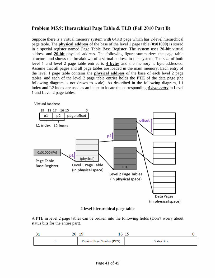
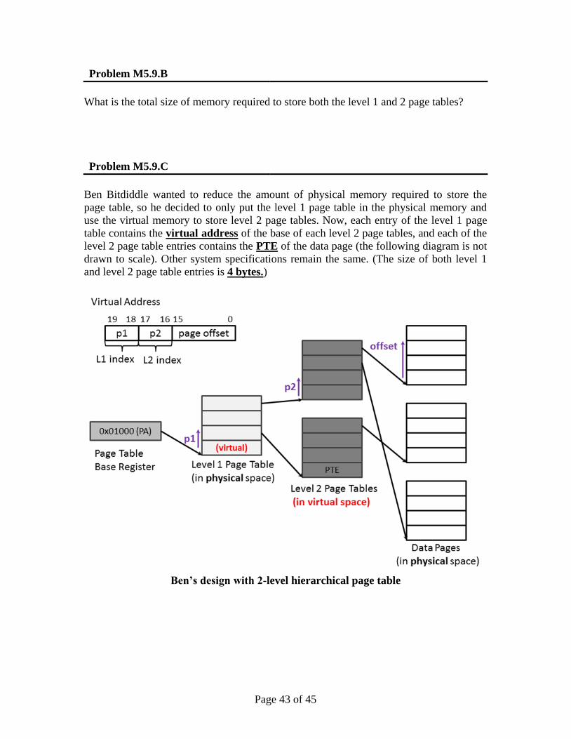
Problem M5.9: Hierarchical Page Table & TLB (Fall 2010 Part B)
Suppose there is a virtual memory system with 64KB page which has 2-level hierarchical
page table. The physical address of the base of the level 1 page table (0x01000) is stored
in a special register named Page Table Base Register. The system uses 20-bit virtual
address and 20-bit physical address. The following figure summarizes the page table
structure and shows the breakdown of a virtual address in this system. The size of both
level 1 and level 2 page table entries is 4 bytes and the memory is byte-addressed.
Assume that all pages and all page tables are loaded in the main memory. Each entry of
the level 1 page table contains the physical address of the base of each level 2 page
tables, and each of the level 2 page table entries holds the PTE of the data page (the
following diagram is not drawn to scale). As described in the following diagram, L1
index and L2 index are used as an index to locate the corresponding 4-byte entry in Level
1 and Level 2 page tables.
2-level hierarchical page table
A PTE in level 2 page tables can be broken into the following fields (Don’t worry about
status bits for the entire part).
Page 42 of 45
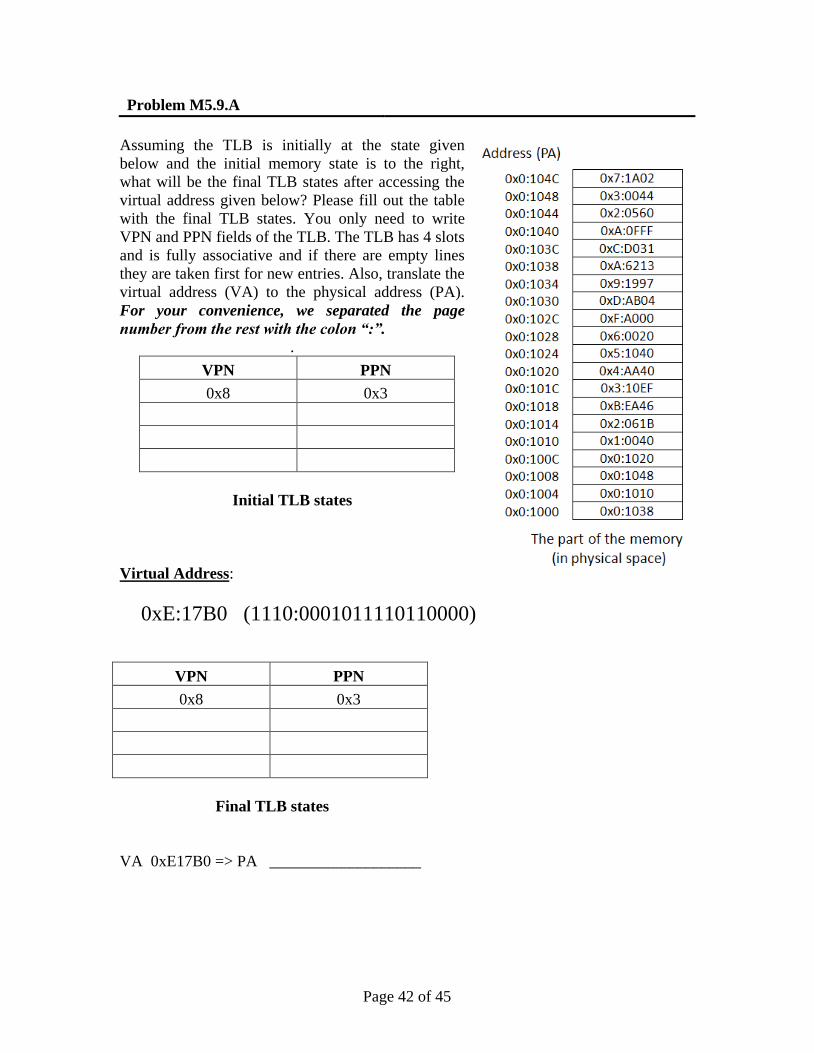
Problem M5.9.A
Assuming the TLB is initially at the state given
below and the initial memory state is to the right,
what will be the final TLB states after accessing the
virtual address given below? Please fill out the table
with the final TLB states. You only need to write
VPN and PPN fields of the TLB. The TLB has 4 slots
and is fully associative and if there are empty lines
they are taken first for new entries. Also, translate the
virtual address (VA) to the physical address (PA).
For your convenience, we separated the page
number from the rest with the colon “:”.
.
VPN PPN
0x8 0x3
Initial TLB states
Virtual Address:
0xE:17B0 (1110:0001011110110000)
VPN PPN
0x8 0x3
Final TLB states
VA 0xE17B0 => PA ___________________
Page 43 of 45
Problem M5.9.B
What is the total size of memory required to store both the level 1 and 2 page tables?
Problem M5.9.C
Ben Bitdiddle wanted to reduce the amount of physical memory required to store the
page table, so he decided to only put the level 1 page table in the physical memory and
use the virtual memory to store level 2 page tables. Now, each entry of the level 1 page
table contains the virtual address of the base of each level 2 page tables, and each of the
level 2 page table entries contains the PTE of the data page (the following diagram is not
drawn to scale). Other system specifications remain the same. (The size of both level 1
and level 2 page table entries is 4 bytes.)
Ben’s design with 2-level hierarchical page table
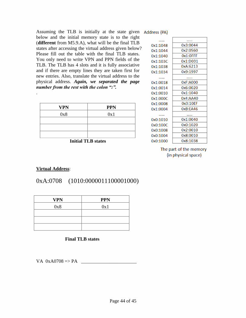
Page 44 of 45
Assuming the TLB is initially at the state given
below and the initial memory state is to the right
(different from M5.9.A), what will be the final TLB
states after accessing the virtual address given below?
Please fill out the table with the final TLB states.
You only need to write VPN and PPN fields of the
TLB. The TLB has 4 slots and it is fully associative
and if there are empty lines they are taken first for
new entries. Also, translate the virtual address to the
physical address. Again, we separated the page
number from the rest with the colon “:”.
.
Initial TLB states
Virtual Address:
0xA:0708 (1010:0000011100001000)
VPN PPN
0x8 0x1
Final TLB states
VA 0xA0708 => PA _______________________
VPN PPN
0x8 0x1
Page 45 of 45
Problem M5.9.D
Alice P. Hacker examines Ben’s design and points out that his scheme can result in
infinite loops. Describe the scenario where the memory access falls into infinite loops.