Printed Electronics Limited - lboro.ac.uk Printing of Electronics ... Ag Ink and transparent...
49
© PEL 2010 IeMRC 21 Sept 2010 PEL is focussed on the development, characterisation and manufacture of electronic circuits and devices using materials and functional inks deployed by inkjet and direct writing. Steve Jones [email protected] www.printedelectronics.com
-
Upload
nguyenkien -
Category
Documents
-
view
216 -
download
3
Transcript of Printed Electronics Limited - lboro.ac.uk Printing of Electronics ... Ag Ink and transparent...

© PEL 2010 IeMRC 21 Sept 2010 PEL is focussed on the development, characterisation and manufacture of electronic circuits and devices using materials and functional inks deployed by inkjet and direct writing.
Steve Jones [email protected]
www.printedelectronics.com

Digital Printing of Electronics Putting electronics in new places
PEL is focussed on the development, characterisation and manufacture of electronic circuits and devices using materials and functional inks deployed by inkjet and direct writing
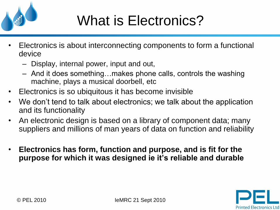
What is Electronics?
• Electronics is about interconnecting components to form a functional device
– Display, internal power, input and out,
– And it does something…makes phone calls, controls the washing machine, plays a musical doorbell, etc
• Electronics is so ubiquitous it has become invisible
• We don’t tend to talk about electronics; we talk about the application and its functionality
• An electronic design is based on a library of component data; many suppliers and millions of man years of data on function and reliability
• Electronics has form, function and purpose, and is fit for the purpose for which it was designed ie it’s reliable and durable
© PEL 2010 IeMRC 21 Sept 2010

What is Printed Electronics?
• Circuitry created with conductive and/or electro-active inks using a
wide variety of printing techniques ie the inks are the components
usually in the form of nano-particles in a carrier that gives an
appropriate surface tension and viscosity for the printing method.
• We presently do not have a library of component data; few suppliers and little data on function and reliability
• However, printed electronics must form, function and purpose, and is fit for the purpose for which it was designed ie it’s reliable and durable
© PEL 2010 IeMRC 21 Sept 2010

Printed Electronics Limited (PEL)
• PEL is a process development company
– Using in house facilities for proof of concept through to pre-production level.
– Develop/specify systems, processes and material sets for use in end-customer operation at production level.
• Mainly developing inkjet-electronics and material deposition by inkjet techniques:
– Circuit printing, dielectric application, display printing
• Management of PEL have long experience in PCB manufacturing and semiconductor development.
• Offices in Cambridge and Tamworth, UK
– Team of industry specialists.
• Developing processes for a number of clients
IeMRC 21 Sept 2010 © PEL 2010

Print techniques
SCREEN INKJET
© PEL 2010 IeMRC 21 Sept 2010
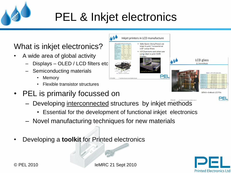
PEL & Inkjet electronics
What is inkjet electronics? • A wide area of global activity
– Displays – OLED / LCD filters etc
– Semiconducting materials
• Memory
• Flexible transistor structures
• PEL is primarily focussed on
– Developing interconnected structures by inkjet methods
• Essential for the development of functional inkjet electronics
– Novel manufacturing techniques for new materials
• Developing a toolkit for Printed electronics
© PEL 2010 IeMRC 21 Sept 2010

Why inkjet electronics?
© PEL 2010 IeMRC 21 Sept 2010

IeMRC 21 Sept 2010
Why … ?
(Inkjet is not always the best method for printing of electronics…
e.g. we also CHOOSE to use screen print and nozzle dispensing)
• Inkjet is truly additive
• No hard tooling
• Non-contact
• In an inkjet electronic world (and in plastic electronics generally) electronics don’t have to be flat and neither do they have to be flexible
– Designers love flexible electronics
• Printed (including inkjet) electronics doesn’t have to look like conventional electronics eg combine with graphics
– It can be curved, low cost, can be disposable with low environmental burden.
– It can be used on packaging, advertising, clothing etc
© PEL 2010

IeMRC 21 Sept 2010
The Advantages of Inkjet
Electronics
…or “the new things that can be done”
© PEL 2010

IeMRC 21 Sept 2010
Multilayer PCB entirely by inkjet
7 layer structure:
1. Silver (base)
2. Dielectric 1
3. Silver
4. Dielectric 2
5. Silver
6. Dielectric 3
7. Silver
Note – vias are not
necessarily round
Status – State of the art (proof of concept) © PEL 2010

IeMRC 21 Sept 2010
Very long circuits (single layer on PET )
• Reel-to-reel continuous printing – potentially 2km in single print
• Digital image can be changed dynamically
• Cannot be done by conventional panel processing methods
• Application – printed sensors etc
• Status – available now from CIT. Plated Cu on PET. – CIT process is predominant method for reel to reel inkjet electronics (www.inkjetflex.com)
© PEL 2010

Circuits on wearable fabric
Circuits in clothing:
Check www.CuteCircuit.com
• Application
– Fashion, communications etc
• Status
– in development at PEL and
elsewhere
© PEL 2010 IeMRC 21 Sept 2010

Inkjet’s high precision drop placement
(i) Security application
• Precise drop volume;
each droplet can be
placed with a precision of
~m to each other
• Functional materials
• Pharmaceutical or
tracer/marker materials
• Application – identity
protection, covert and
overt security.
• Status – available now
(PEL).
Machine-readable “single pixel” 2D barcode.
Hidden Marking application
© PEL 2010 IeMRC 21 Sept 2010

Inkjet’s high precision drop placement
(ii) transistor interconnect
IeMRC 21 Sept 2010
Printed Ag lines are 35um in width
Printed drop size is 1pl
Ag Ink and transparent insulator
With kind permission of Nanoeprint
Status – proof of concept
(pre-production capable)
© PEL 2010

Benefits of non contact printing
- Printing into recesses
• Application
– Printing where conventional contact print methods cannot be used
• Status
– Available for compatible structures only
© PEL 2010 IeMRC 21 Sept 2010

Highly curved surfaces Aerospace Helmet
PEL have developed this
system as a proof of
concept for doubly curved
surfaces.
System builders (such as
Xennia) have commercial
systems with multi axis
robots to control 3D printing.
PEL System
© PEL 2010 IeMRC 21 Sept 2010

Applicable methods for packaging
© PEL 2010 IeMRC 21 Sept 2010

Direct Conductive Print (DCP) on paper, plastics and ceramics
e.g.
• Developed a process to achieve conductivity on low cost paper based substrates etc without high temperature cure.
• Circuit structures manufactured in < 1 minute
• Cure in seconds (heat or photonic)
• Application – Non contact printing of circuitry
• Status – Process available for prototype
and pre-production level.
© PEL 2010 IeMRC 21 Sept 2010

© PEL 2010
Printing in CMY
• PEL Array head designed to allow
simultaneous printing of different
inks.
Applications
• Graphics and electronics – print colour graphics to hide electronic
circuits or other features
• Print chemically reactive species
to form chemical reactions on a
substrate
• Biological: simultaneously print a
range of biologically active
material – can change the printed area and
concentration of functional materials
Status – proto-production
• Metals:
– Au
– Ni
– Ag
– Cu
– Si
On PEL-paper substrate, nano metal inks
will functionalise to become conductive
with 120°C fast cure or pulsed xenon flash
K Ag Cu Au K
IeMRC 21 Sept 2010

Printed Displays (EL)
• Direct print onto substrate (ie paper, plastic etc)
With the “right” substrate - very high definition images can be produced .
Pixel size ~60µm on “PEL coated
paper”
• Application –
marketing/branding
• Status – available with inkjet
and screen print methods.
© PEL 2010 IeMRC 21 Sept 2010

Graphics + Electronics
• Combination of colour graphic
printing with circuit designs.
– Packaging
– Branding
– “attractors” for trade shows etc
• Application
– Branding graphics
– Overprinting - printed onto
assembled components
• Status
– Available
© PEL 2010 IeMRC 21 Sept 2010

So it can be done….
How do we do it?
© PEL 2010 IeMRC 21 Sept 2010

Inkjet Electronics
• The fundamentals of inkjet printing
of interconnects involves 4 basic
elements or processes.
– Head
– Ink
– Substrate
– Functionalisation
and, of course, a Print Platform
ink
head
substrate
© PEL 2010 IeMRC 21 Sept 2010
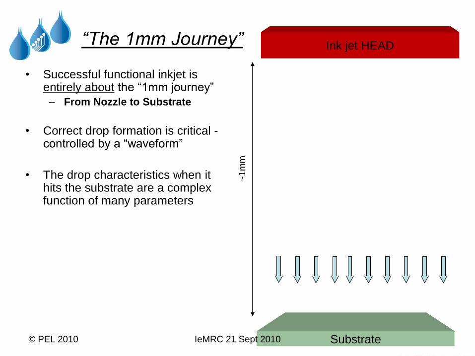
Ink jet HEAD
• Successful functional inkjet is entirely about the “1mm journey”
– From Nozzle to Substrate
• Correct drop formation is critical - controlled by a “waveform”
• The drop characteristics when it hits the substrate are a complex function of many parameters
“The 1mm Journey”
Substrate
~1m
m
© PEL 2010 IeMRC 21 Sept 2010

Inside an inkjet head (Xaar1001)
Toolkit item: YES
© PEL 2010 IeMRC 21 Sept 2010
#1 Consideration
Whatever ink one chooses to print must be
compatible with the head and give long term
reliability.
© PEL 2010 IeMRC 21 Sept 2010

Inks for electronics applications
© PEL 2010 IeMRC 21 Sept 2010
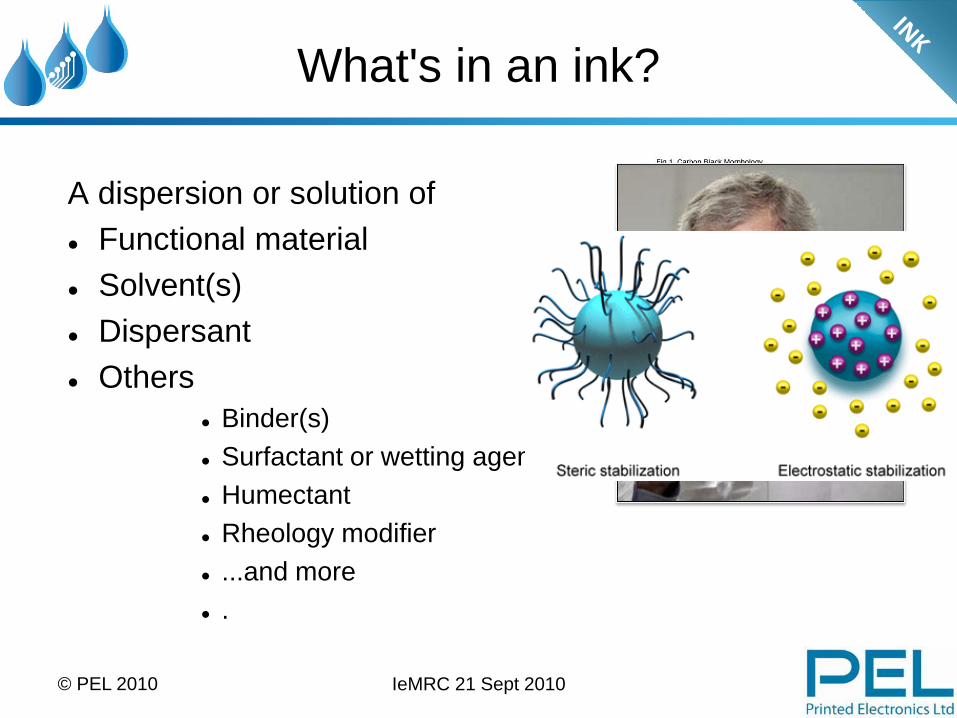
What's in an ink?
A dispersion or solution of
Functional material
Solvent(s)
Dispersant
Others
Binder(s)
Surfactant or wetting agent(s)
Humectant
Rheology modifier
...and more
.
© PEL 2010 IeMRC 21 Sept 2010

Ideal Characteristics for an inkjet ink
Surface tension 20 to 30 Dynes/cm
Viscosity range 8 to 12 cps
© PEL 2010 IeMRC 21 Sept 2010

What is in a typical nano-metal ink?
• It is a liquid mixture of:
– what I want to keep
• i.e. Ag, Cu, Au, Ni particles
– what I must get rid of
• i.e. organic solvents,
stabilisers, viscosity
additives.
– Generally the list of “what I
want to keep” is shorter…
• A 40% by weight silver ink
is 4% by volume; therefore
96% of the ink volume has
to “disappear”. Solvents can
disappear but dispersion
agents tend to hang around.
© PEL 2010 IeMRC 21 Sept 2010
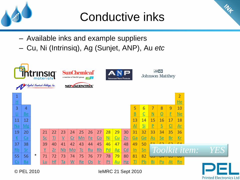
Conductive inks
– Available inks and example suppliers
– Cu, Ni (Intrinsiq), Ag (Sunjet, ANP), Au etc
1 H
2 He
3 Li
4 Be
5 B
6 C
7 N
8 O
9 F
10 Ne
11 Na
12 Mg
13 Al
14 Si
15 P
16 S
17 Cl
18 Ar
19 K
20 Ca
21 Sc
22 Ti
23 V
24 Cr
25 Mn
26 Fe
27 Co
28 Ni
29 Cu
30 Zn
31 Ga
32 Ge
33 As
34 Se
35 Br
36 Kr
37 Rb
38 Sr
39 Y
40 Zr
41 Nb
42 Mo
43 Tc
44 Ru
45 Rh
46 Pd
47 Ag
48 Cd
49 In
50 Sn
51 Sb
52 Te
53 I
54 Xe
55 Cs
56 Ba
* 71 Lu
72 Hf
73 Ta
74 W
75 Re
76 Os
77 Ir
78 Pt
79 Au
80 Hg
81 Tl
82 Pb
83 Bi
84 Po
85 At
86 Rn
Toolkit item: YES
© PEL 2010 IeMRC 21 Sept 2010

Dielectric Inks
• Printable dielectrics
– Acrylic systems
– Epoxy systems
– Polyimide
– SU-8 (Popular in inkjet
applications)
• Choice of dielectric is highly
dependent on substrate and
conductive ink combinations .
Toolkit item: YES
© PEL 2010 IeMRC 21 Sept 2010

Platform
• Dimatix DMP 2800
• Dimatix DMP 3000
• Microcraft
• DGI/Dilli (Korea)
• iTi
• Samsung
• PixDro
• CeraDrop etc
• Costs vary from £30k to
£250k for a basic system.
• Decision is very
dependent on the inkjet
head and market that will
be your main focus.
Toolkit item: YES
© PEL 2010 IeMRC 21 Sept 2010

Substrates for electronic
applications
© PEL 2010 IeMRC 21 Sept 2010

Common substrates for Printed Electronics
• Polyimide – High temperature resistance widely used in electronics
• FR4 – Epoxy resin reinforced with woven e-glass
• Cu – Electroplated foil
– Brushed surface
– etc
• Glass and Plastics – Display applications
For packaging applications
• Paper
• Plastic (PET, PEN etc)
© PEL 2010 IeMRC 21 Sept 2010

Comparison of drop sizes in flight and on substrate
• Drop volume V, Drop radius r
• Drop on surface
– Rule of thumb:
• 2 ~ 4 times diameter in flight
3
3
4rV
8pl ~ 24um
8pl ~ 50~60um
© PEL 2010 IeMRC 21 Sept 2010

IeMRC 21 Sept 2010
Interactions of Nano Ag on Paper
With thanks to Cambridge University IfM
A PEL Partner

IeMRC 21 Sept 2010
It’s PAPER Jim, but not as we know it
Ag
Coated Paper
• One can use “photo-
paper-like” substrates
for conductor printing.
– Not all photo-paper
works well.
• Surface structure is
critical to the
performance.
• Specialist paper is
required.
Toolkit item: YES
© PEL 2010

Next process steps
• Sintering of the printed metallic layers
– Sintering: Bonding of adjacent surfaces of particles by heating
– To make the layer conduct
• Curing dielectric materials
– By UV exposure etc
• Drying layers
– Thermal/Xe
All of which is termed “Functionalisation”
ink substrate
© PEL 2010 IeMRC 21 Sept 2010

Functionalisation
• Method employed is dependent on
the material being deposited
– Nano metal ink ALWAYS require
sintering
• With the right substrate and ink the
sintering temperature can be
120~140°C
• High energy UV flash is very effective
– UV curing materials (i.e. dielectric):
• Decide on UV pin or UV cure
• Very different behaviour can be
generated
– Especially important for multilayer
structures.
www.nanomastech.com
PEL UV Cured 3D structures
© PEL 2010 IeMRC 21 Sept 2010

NanoAg Functionalisation
• Paper based substrate
• Flash heated to 140C for
a few seconds
• Pulsed Xe flash 1ms
• Forms a continuous layer
of Ag with low resistance
– 16% and up of bulk silver
value
Ag
Paper substrate
Time (60s)
© PEL 2010 IeMRC 21 Sept 2010

Pieces of the puzzle
SUB- STRATE
INTERCONNECT Ink
Process Functionalise Interconnect
Function
Conductive Epoxies etc
FULL PRODUCT Conventional Components
• Successful printed
electronic demonstrators
rely (for the foreseeable
future ) upon conventional
electronic components
too.
• Combining successfully
the required elements is
the key to functional,
reliable products.
IeMRC 21 Sept 2010 © PEL 2010

Industrial Process Development
Key Considerations
• Cost benefit • Fixed cost and variable cost elements
• Robustness of process – Variation in materials
• One supplier for (eg) substrate + ink – early stage ok
– Later maybe not
• Is the scale suitable for inkjet?
– Materials developers point of view • Have you considered the requirements for “electronic” applications
• Nanomaterials – particle size / batch release
© PEL 2010 IeMRC 21 Sept 2010

Cost considerations
• Is inkjet the right solution for your application? – What must the process
provide?
– Is it better or “just different”
– Financially – is the process sound
– >> cost calculator for single layer nano Ag circuits
Cost Elements
Image size (mm) 80 80
DPI 309
% of image that is black 20%
Number of passes 3
HEAD - Drop volume (pl) 50
INK - Cost per litre (£) 3500
Number of dots in X 973
Number of dots in Y 973
Number of dots (using % of black) 568,304
Volume of ink used (ml) 0.0284
Cost of circuit (£) £0.10
© PEL 2010 IeMRC 21 Sept 2010

Conclusion
• Inkjet has no tooling, it is a fully additive digital process.
– Offers products and processes that are impossible by any other
means
– Start-up costs are low.
• Inkjet printing can deliver a very precise amount of
material to a specific location on almost any material
(e.g. for electronic or pharmaceutical applications)
• Printed electronics can add value to packaging.
© PEL 2010 IeMRC 21 Sept 2010
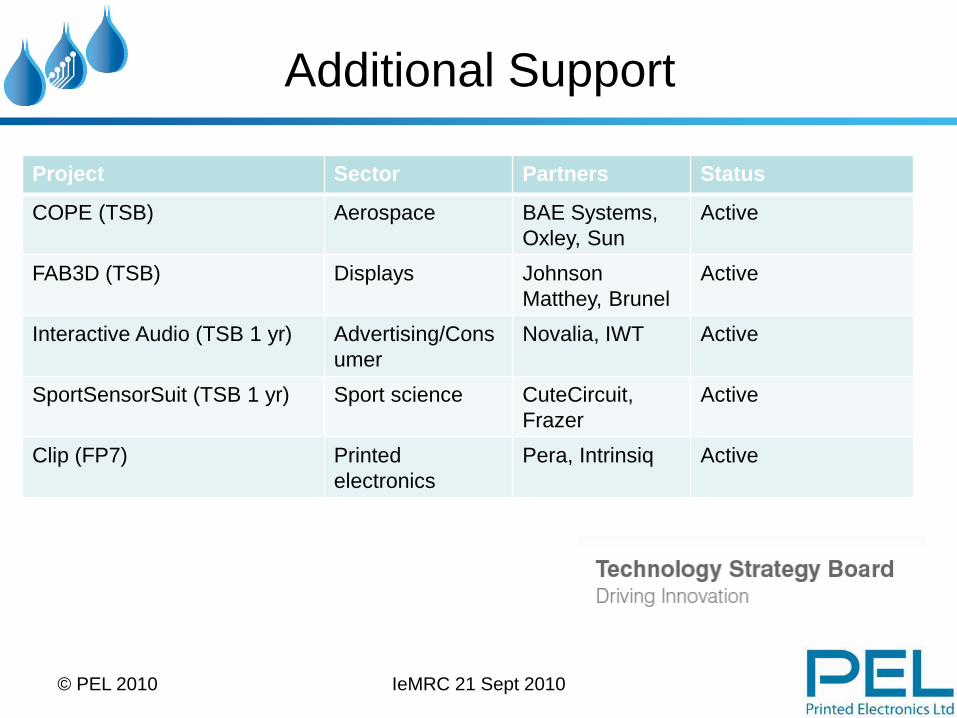
Additional Support
Project Sector Partners Status
COPE (TSB) Aerospace BAE Systems,
Oxley, Sun
Active
FAB3D (TSB) Displays Johnson
Matthey, Brunel
Active
Interactive Audio (TSB 1 yr) Advertising/Cons
umer
Novalia, IWT Active
SportSensorSuit (TSB 1 yr) Sport science CuteCircuit,
Frazer
Active
Clip (FP7) Printed
electronics
Pera, Intrinsiq Active
© PEL 2010 IeMRC 21 Sept 2010

Thank You
© PEL 2010 IeMRC 21 Sept 2010

IeMRC 21 Sept 2010
Blatant Advert… PEL “InkTronics” courses
Inkjet Electronics 101 • Basic ink rheology of electronically functional/nanoparticulate inkjet
inks
• Introduction to binary and greyscale technology inkjet heads
• Drop visualisation and satellite formation
• Ink drop/substrate interaction and spread characteristics
• Substrate surface modification
• Printing and functionalisation of electronically functional inks using Dimatix DMP and Xaar equipped iTi printing systems. The course is practically based and the participants will use our drop visualisation, surface energy modification equipment and inkjet machines to print and functionalise simple circuits.
Contact us [email protected]
© PEL 2010