PRIME: A Novel Processing-in-memory … - Scalable Energy-Efficient Architecture Lab Scalable and...
26
UCSB - Scalable Energy-Efficient Architecture Lab Scalable and Energy-Efficient Architecture Lab (SEAL) PRIME: A Novel Processing-in-memory Architecture for Neural Network Computation in ReRAM-based Main Memory Ping Chi * , Shuangchen Li * , Tao Zhang † , Cong Xu ‡ , Jishen Zhao δ , Yu Wang # , Yongpan Liu # , Yuan Xie * * Electrical and Computer Engineering Department University of California, Santa Barbara † Nvidia, ‡ HP Labs, δ University of California, Santa Cruz # Tsinghua University, Beijing, China 1
Transcript of PRIME: A Novel Processing-in-memory … - Scalable Energy-Efficient Architecture Lab Scalable and...

UCSB - Scalable Energy-Efficient Architecture Lab
Scalable and Energy-Efficient Architecture Lab (SEAL)
PRIME: A Novel Processing-in-memory Architecture for Neural Network Computation
in ReRAM-based Main Memory
Ping Chi*, Shuangchen Li*, Tao Zhang†, Cong Xu‡, Jishen Zhaoδ, Yu Wang#, Yongpan Liu#, Yuan Xie*
*Electrical and Computer Engineering Department
University of California, Santa Barbara
†Nvidia, ‡HP Labs, δ University of California, Santa Cruz #Tsinghua University, Beijing, China
1

Motivation
• Challenges– Data movement is expensive
– Applications demand large memory bandwidth
• Processing-in-memory (PIM)– Minimize data movement by placing
computation near data or in memory
– 3D stacking revives PIM
2Micron, “Hybrid Memory Cube”, HC’11
• Embrace the large internal
data transfer bandwidth
• Reduce the overheads of
data movement

Motivation
• Neural network (NN) and deep learning (DL)– Provide solutions to various applications
– Acceleration requires high memory bandwidth
• PIM is a promising solution
3
Deng et al, “Reduced-Precision Memory Value
Approximation for Deep Learning”, HPL Report, 2015
• The size of NN increases
• e.g., 1.32GB synaptic
weights for Youtube video
object recognition
• NN acceleration
• GPU, FPGA, ASIC
• ReRAM crossbar

Motivation
• Resistive Random Access Memory (ReRAM)
– Data storage: alternative to DRAM and flash
– Computation: matrix-vector multiplication (NN)
4
Hu et al, “Dot-Product Engine (DPE) for Neuromorphic Computing: Programming
1T1M Crossbar to Accelerate Matrix-Vector Multiplication”, DAC’16.
Shafiee et al, “ISAAC: A Convolutional Neural Network Accelerator with In-
Situ Analog Arithmetic in Crossbars”, ISCA’16.
• Use DPE to accelerate pattern recognition on MNIST
• no accuracy degradation vs. software approach (99% accuracy) with only 4-bit DAC and ADC requirement
• 1,000X ~ 10,000X speed-efficiency product vs. custom digital ASIC
Key idea
• PRIME: processing in ReRAM main memory
– Based on ReRAM main memory design[1]
5
[1] Xu et al, “Overcoming the challenges of crossbar resistive memory architectures,” in
HPCA’15.
Memory Mode
Comp. Modew1,1
b1
w2,1
w3,1
a1
a2
a3
w1,2
b2
w2,2
w3,2
Store Data
Store Weight
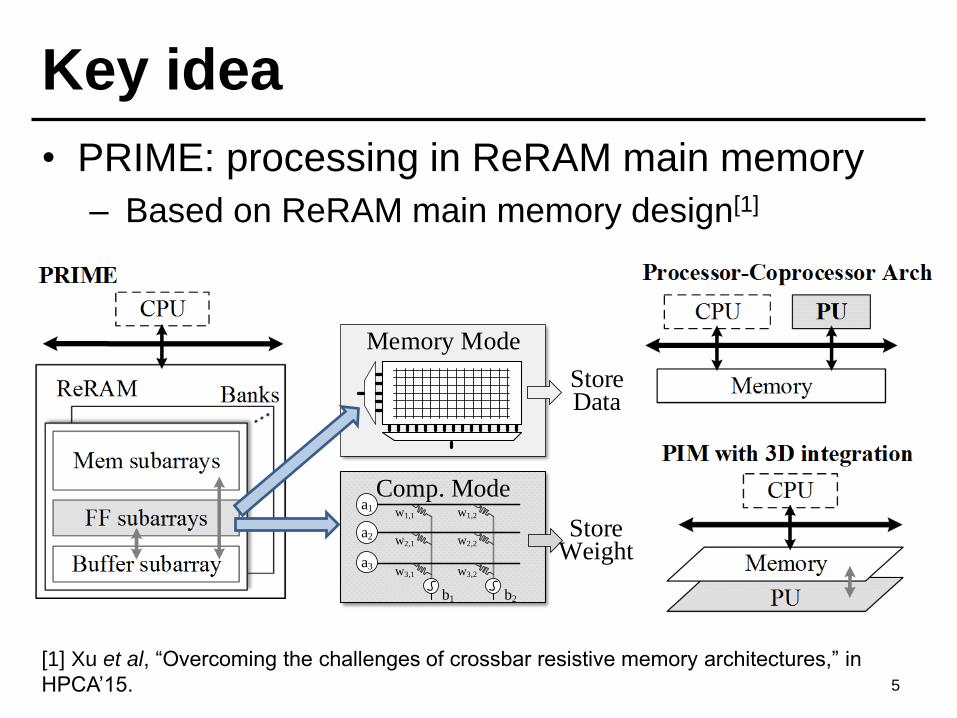
ReRAM Basics
6
Top Electrode
Metal Oxide
Bottom Electrode
Voltage
HRS (‘0’)
LRS (‘1’)
SET
RESET
Voltage
Wordline
Cell
(a) Conceptual view
of a ReRAM cell
(b) I-V curve of bipolar
switching
(c) schematic view of a
crossbar architecture
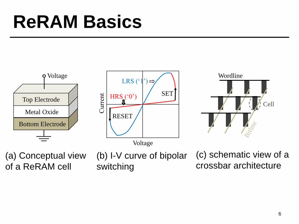
ReRAM Based NN Computation
• Require specialized peripheral circuit design
• DAC, ADC etc.
7
(a) An ANN with one input and one output layer
a1
a2
+ b1
w1,1
w2,1
w1,2
w2,2+ b2
(b) using a ReRAM crossbar array for neural computation
w1,1
w2,1
w1,2
w2,2
b1 b2
a1
a2
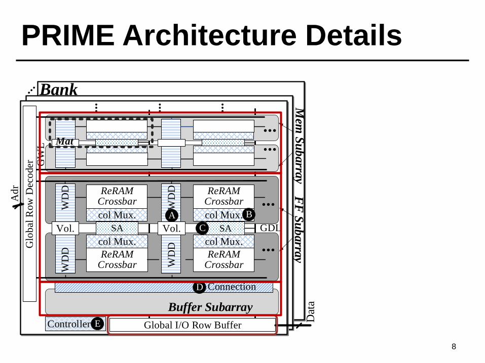
PRIME Architecture Details
8
Glo
bal
Row
Dec
oder
Global I/O Row Buffer
Dat
a
Ad
r
Bank
FF
Su
barra
y
ReRAM Crossbar
ReRAM Crossbar
SA
ReRAM Crossbar
ReRAM Crossbar
Mem
Su
barra
y
D Connection
Controller E
GW
L Mat
Buffer Subarray
C
A
SA
col Mux. col Mux.
col Mux. col Mux. B
WD
D
Vol.Vol. GDL
WD
D
WD
DW
DD

PRIME Architecture Details
9
Glo
bal
Row
Dec
oder
Global I/O Row Buffer
Dat
a
Ad
r
Bank
FF
Su
barra
y
ReRAM Crossbar
ReRAM Crossbar
SA
ReRAM Crossbar
ReRAM Crossbar
Mem
Su
barra
y
D Connection
Controller E
GW
L Mat
Buffer Subarray
C
A
SA
col Mux. col Mux.
col Mux. col Mux. B
WD
D
Vol.Vol. GDL
WD
D
WD
DW
DD
A. Wordline decoder and
driver with multi-level
voltage sources;
B. column multiplexer
with analog subtraction
and sigmoid circuitry;
C. reconfigurable SA with
counters for multi-level
outputs, and added
ReLU and 4-1 max
pooling function units;
D. connection between
the FF and Buffer
subarrays;
E. PRIME controller.

PRIME Architecture Details
10
Glo
bal
Row
Dec
oder
Global I/O Row Buffer
Dat
a
Ad
r
Bank
FF
Su
barra
y
ReRAM Crossbar
ReRAM Crossbar
SA
ReRAM Crossbar
ReRAM Crossbar
Mem
Su
barra
y
D Connection
Controller E
GW
L Mat
Buffer Subarray
C
A
SA
col Mux. col Mux.
col Mux. col Mux. B
WD
D
Vol.Vol. GDL
WD
D
WD
DW
DD
A. Wordline decoder and
driver with multi-level
voltage sources;
B. column multiplexer
with analog subtraction
and sigmoid circuitry;
C. reconfigurable SA with
counters for multi-level
outputs, and added
ReLU and 4-1 max
pooling function units;
D. connection between
the FF and Buffer
subarrays;
E. PRIME controller.

Overcome Precision Challenges
• Technology limitation
– Input precision (input voltage, DAC)
– Weight precision (MLC level)
– Output precision (analog computation, ADC)
• Propose input and synapse composing scheme
– Compose multiple low-precision input signals for one
– Compose multiple cells for one weight
– Compose multiple phases for one computation
11
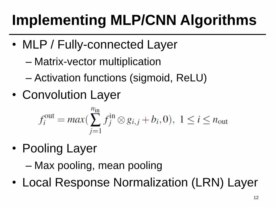
Implementing MLP/CNN Algorithms
• MLP / Fully-connected Layer
– Matrix-vector multiplication
– Activation functions (sigmoid, ReLU)
• Convolution Layer
• Pooling Layer
– Max pooling, mean pooling
• Local Response Normalization (LRN) Layer12
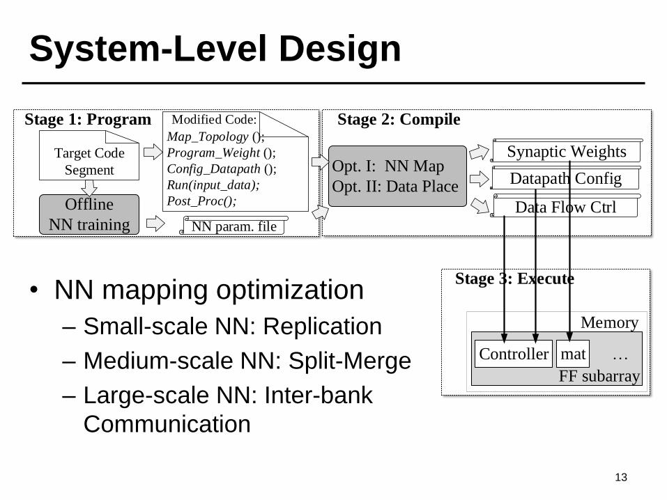
System-Level Design
13
Target Code
Segment
Offline
NN training
Stage 1: Program
NN param. file
Opt. I: NN Map
Opt. II: Data Place
Synaptic Weights
Datapath Config
Data Flow Ctrl
Map_Topology ();
Program_Weight ();
Config_Datapath ();
Run(input_data);
Post_Proc();
Modified Code:
PRIME
Stage 3: Execute
Stage 2: Compile
Controller mat …
Memory
FF subarray
• NN mapping optimization
– Small-scale NN: Replication
– Medium-scale NN: Split-Merge
– Large-scale NN: Inter-bank
Communication
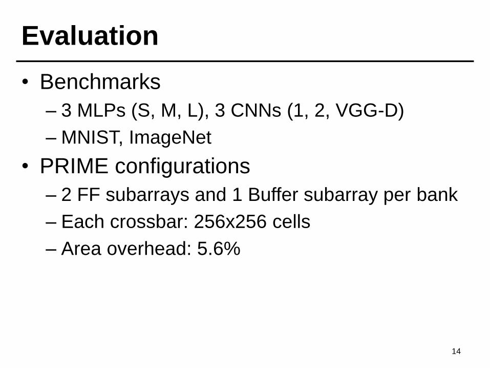
Evaluation
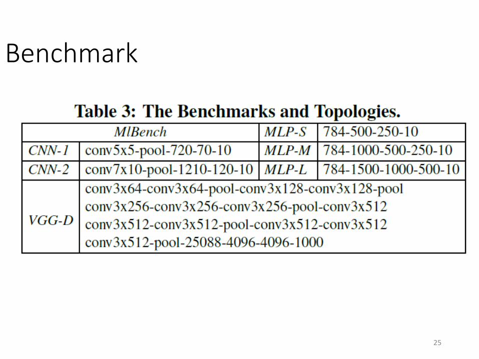
• Benchmarks
– 3 MLPs (S, M, L), 3 CNNs (1, 2, VGG-D)
– MNIST, ImageNet
• PRIME configurations
– 2 FF subarrays and 1 Buffer subarray per bank
– Each crossbar: 256x256 cells
– Area overhead: 5.6%
14

Evaluation
• Comparisons– Baseline CPU-only, pNPU-co, pNPU-pim
15
[1]
[1] T. Chen et al., “DianNao: A small-footprint high-throughput accelerator for
ubiquitous machine-learning,” in ASPLOS’14.

Performance results
16
• PRIME is even 4x better than pNPU-pim-x64
8.2
6.0
4.0 5.5 8.5
1.7
5.0
42
.4
33
.3
55
.1
88
.4
14
7.5
8.5
45
.3
27
16
21
29
35
27
56
58
94
40
54
5
28
99
51
01
58
24
17
66
5
44
04
3
73
23
7
15
96 1
18
02
1E+00
1E+01
1E+02
1E+03
1E+04
1E+05
CNN-1 CNN-2 MLP-S MLP-M MLP-L VGG gmean
Spee
dup
Norm
. to
CP
U
pNPU-co pNPU-pim-x1 pNPU-pim-x64 PRIME
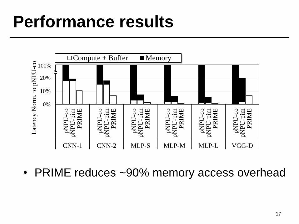
Performance results
17
• PRIME reduces ~90% memory access overhead
0%
10%
20%
30%p
NP
U-c
op
NP
U-p
imP
RIM
E
pN
PU
-co
pN
PU
-pim
PR
IME
pN
PU
-co
pN
PU
-pim
PR
IME
pN
PU
-co
pN
PU
-pim
PR
IME
pN
PU
-co
pN
PU
-pim
PR
IME
pN
PU
-co
pN
PU
-pim
PR
IME
CNN-1 CNN-2 MLP-S MLP-M MLP-L VGG-D
Lat
ency
No
rm.
to p
NP
U-c
o
Compute + Buffer Memory100%
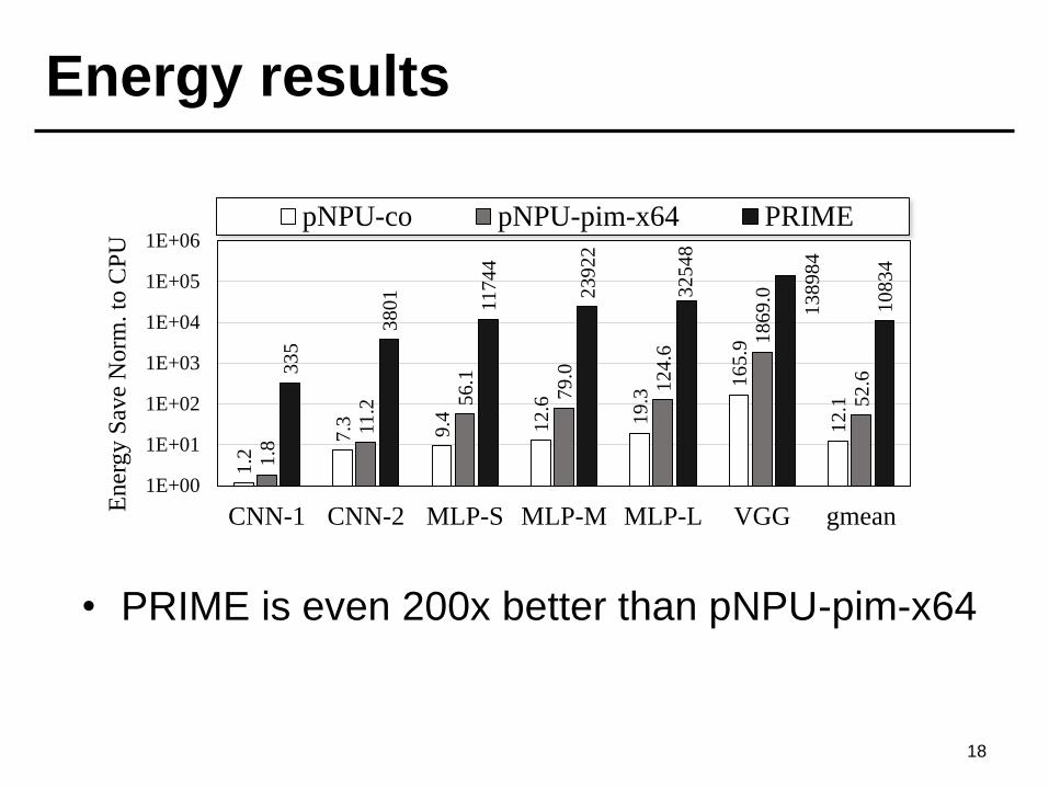
Energy results
18
• PRIME is even 200x better than pNPU-pim-x64
1.2
7.3 9.4 12
.6
19
.3
16
5.9
12
.1
1.8
11
.2 56
.1
79
.0
12
4.6
18
69
.0
52
.6
33
5
38
01
11
74
4
23
92
2
32
54
8
13
89
84
10
83
4
1E+00
1E+01
1E+02
1E+03
1E+04
1E+05
1E+06
CNN-1 CNN-2 MLP-S MLP-M MLP-L VGG gmean
En
erg
y S
ave
Norm
. to
CP
U
pNPU-co pNPU-pim-x64 PRIME
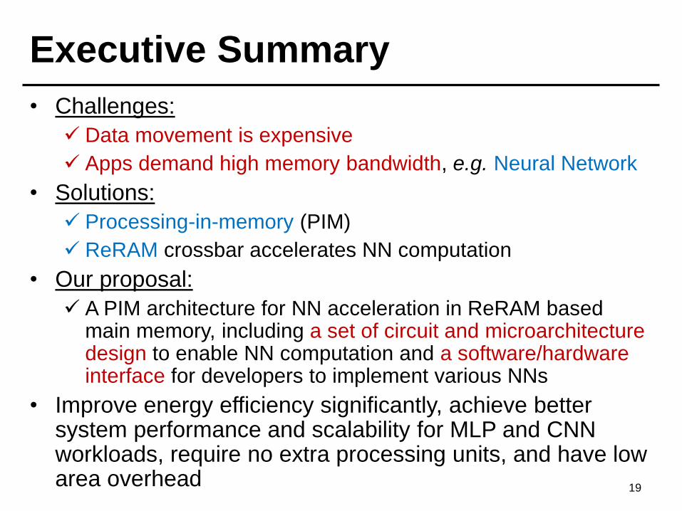
Executive Summary
• Challenges:
Data movement is expensive
Apps demand high memory bandwidth, e.g. Neural Network
• Solutions:
Processing-in-memory (PIM)
ReRAM crossbar accelerates NN computation
• Our proposal:
A PIM architecture for NN acceleration in ReRAM based main memory, including a set of circuit and microarchitecture design to enable NN computation and a software/hardware interface for developers to implement various NNs
• Improve energy efficiency significantly, achieve better system performance and scalability for MLP and CNN workloads, require no extra processing units, and have low area overhead 19

20
Thank you!

• Handwritten Digit Recognition Task• LeNet-5 (CNN), MNIST database
• Dynamic fixed point data format
Impact of Input/Weight Precisions
21

Input and synapse Composing Scheme
22

Input and synapse Composing Scheme
23
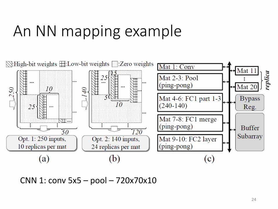
An NN mapping example
24
CNN 1: conv 5x5 – pool – 720x70x10
Benchmark
25
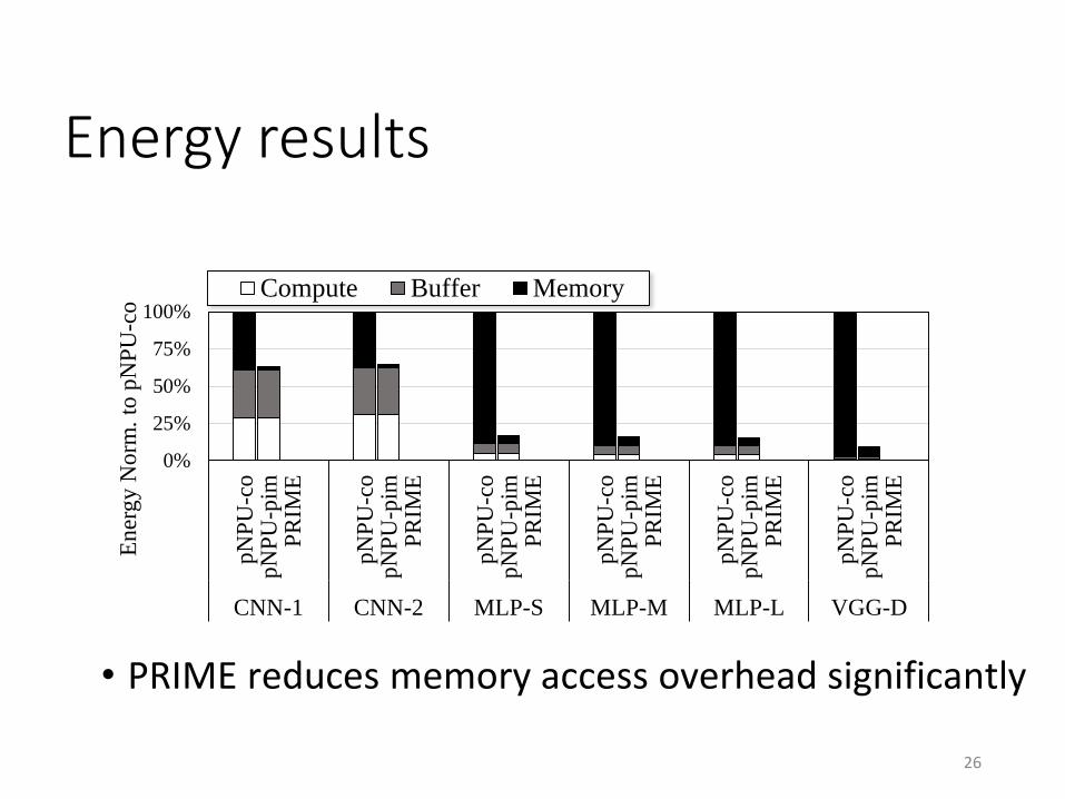
Energy results
26
• PRIME reduces memory access overhead significantly
0%
25%
50%
75%
100%
pN
PU
-co
pN
PU
-pim
PR
IME
pN
PU
-co
pN
PU
-pim
PR
IME
pN
PU
-co
pN
PU
-pim
PR
IME
pN
PU
-co
pN
PU
-pim
PR
IME
pN
PU
-co
pN
PU
-pim
PR
IME
pN
PU
-co
pN
PU
-pim
PR
IME
CNN-1 CNN-2 MLP-S MLP-M MLP-L VGG-D
En
erg
y N
orm
. to
pN
PU
-co
Compute Buffer Memory