Preset the power supply to 14V. Turn off the power Benefits and … · Meets Stringent OEM Module...
8
Evaluates: MAX20034 MAX20034 Evaluation Kit General Description The MAX20034 evaluation kit (EV kit) is a fully assembled and tested application circuit that simplifies the evaluation of the MAX20034 high-efficiency 400kHz/2.2MHz, 36V, dual buck controller IC. This EV kit operates from 3.5V to 42V supply and pro- vides two synchronous step-down outputs by switching at 400kHz/2.2MHz, with each one 180° out of phase from the other. The frequency and output voltages can be adjusted using external resistors. SYNC input program- mability enables three frequency modes for optimized performance: forced fixed-frequency operation, skip mode with ultra-low quiescent current, and synchronized external clock frequency. Benefits and Features ● Dual High-Voltage Step-Down Controllers to Minimize Board-Area Occupancy ● Meets Stringent OEM Module Power Consumption and Performance Specifications ● 17µA Quiescent Current in Skip Mode ● ±1.5% Output-Voltage Accuracy: 5.0V/3.3V, Fixed or Adjustable by External Resistor-Divider ● EMI Reduction Features and Adjustable Fixed- Frequency Operation to Reduce Signal Interference ● Optimized Application Layout and Components for Quick Design Implementation ● Jumpers and Test Points on Key Nodes for Simplified Evaluation ● Proven PCB Layout ● Fully Assembled and Tested 319-100105; Rev 0; 11/17 Ordering Information appears at end of data sheet. Quick Start Required Equipment ● MAX20034 EV kit ● Adjustable DC power supply (PS1) ● Two digital multimeters (DMM1 and DMM2) ● Two electronic loads (EL1 and EL2) Procedure The EV kit is fully assembled and tested. Follow the steps below to verify board operation: 1) Verify that all jumpers are in their default positions, as shown in Table 1. 2) Preset the power supply to 14V. Turn off the power supply. 3) Preset the electronic loads to 2.5A. Turn off the electronic loads. 4) Connect the positive lead of the power supply to the VBATTF PCB pad on the EV kit; connect the negative lead to the neighboring PGND PCB pad. 5) Connect the positive terminal of electronic load EL1 to the VOUT1 PCB pad; connect the negative lead to the PGND1 pad. 6) Connect the positive terminal of electronic load EL2 to the VOUT2 PCB pad; connect the negative lead to the PGND2 PCB pad. 7) Turn on the power supply. 8) Verify that voltage across the VOUT1 and PGND1 PCB pads is 5V, and 3.3V between the VOUT2 and PGND2 PCB pads. 9) Turn on the electronic loads. 10) Verify that voltage across the VOUT1 and PGND PCB pads is 5V ±1.5%. 11) Verify that voltage across the VOUT2 and PGND2 PCB pads is 3.3V ±1.5%. 12) Turn off the electronic loads. 13) Turn off the power supply.
Transcript of Preset the power supply to 14V. Turn off the power Benefits and … · Meets Stringent OEM Module...

Evaluates: MAX20034MAX20034 Evaluation Kit
General DescriptionThe MAX20034 evaluation kit (EV kit) is a fully assembled and tested application circuit that simplifies the evaluation of the MAX20034 high-efficiency 400kHz/2.2MHz, 36V, dual buck controller IC.This EV kit operates from 3.5V to 42V supply and pro-vides two synchronous step-down outputs by switching at 400kHz/2.2MHz, with each one 180° out of phase from the other. The frequency and output voltages can be adjusted using external resistors. SYNC input program-mability enables three frequency modes for optimized performance: forced fixed-frequency operation, skip mode with ultra-low quiescent current, and synchronized external clock frequency.
Benefits and Features Dual High-Voltage Step-Down Controllers to Minimize
Board-Area Occupancy Meets Stringent OEM Module Power Consumption
and Performance Specifications 17µA Quiescent Current in Skip Mode ±1.5% Output-Voltage Accuracy: 5.0V/3.3V, Fixed or
Adjustable by External Resistor-Divider EMI Reduction Features and Adjustable Fixed-
Frequency Operation to Reduce Signal Interference Optimized Application Layout and Components for
Quick Design Implementation Jumpers and Test Points on Key Nodes for Simplified
Evaluation Proven PCB Layout Fully Assembled and Tested
319-100105; Rev 0; 11/17
Ordering Information appears at end of data sheet.
Quick StartRequired Equipment MAX20034 EV kit Adjustable DC power supply (PS1) Two digital multimeters (DMM1 and DMM2) Two electronic loads (EL1 and EL2)
ProcedureThe EV kit is fully assembled and tested. Follow the steps below to verify board operation:1) Verify that all jumpers are in their default positions, as
shown in Table 1.2) Preset the power supply to 14V. Turn off the power
supply.3) Preset the electronic loads to 2.5A. Turn off the
electronic loads.4) Connect the positive lead of the power supply to the
VBATTF PCB pad on the EV kit; connect the negativelead to the neighboring PGND PCB pad.
5) Connect the positive terminal of electronic load EL1to the VOUT1 PCB pad; connect the negative lead tothe PGND1 pad.
6) Connect the positive terminal of electronic load EL2 tothe VOUT2 PCB pad; connect the negative lead to thePGND2 PCB pad.
7) Turn on the power supply.8) Verify that voltage across the VOUT1 and PGND1
PCB pads is 5V, and 3.3V between the VOUT2 andPGND2 PCB pads.
9) Turn on the electronic loads.10) Verify that voltage across the VOUT1 and PGND PCB
pads is 5V ±1.5%.11) Verify that voltage across the VOUT2 and PGND2
PCB pads is 3.3V ±1.5%.12) Turn off the electronic loads.13) Turn off the power supply.
Maxim Integrated 2www.maximintegrated.com
Evaluates: MAX20034MAX20034 Evaluation Kit
Detailed DescriptionThe MAX20034 IC offers two high-voltage synchronous step-down controllers that operate at 180° out-of-phase. This device can be powered up by an input voltage supply from 3.5V to 42V and can operate in drop-out condition by running at 99% duty-cycle. It is intended for applications with mid- to high-power requirements that operate at a wide input voltage range such as during automotive cold-crank or engine stop-start conditions.The IC features a power-OK monitor, overvoltage lock-out, and an undervoltage lockout. Its protection features include cycle-by-cycle current limit and thermal shutdown. It is specified for operation over the -40°C to +125°C auto-motive temperature range.
Switching Frequency and External SynchronizationThe IC can operate in two modes: forced-PWM (FPWM) or skip. Skip mode has better efficiency for light-load con-ditions, while FPWM has fixed switching frequency across all load conditions to prevent unwanted EMI interference. When SYNC is pulled low, the device operates in skip mode for light loads and in PWM mode for heavy loads. When SYNC is pulled high, the device is forced to operate in PWM across all load conditions.SYNC pin can also be used to synchronize with an exter-nal clock frequency. In this case, MAX20034 operates at external clock frequency across all load conditions.
Buck Output Monitoring (PGOOD1, PGOOD2)The EV kit provides power-good output test points (TP_PGOOD1 and TP_PGOOD2) to monitor the status of the buck outputs (VOUT1 and VOUT2). The PGOOD1 and PGOOD2 are set to high impedance when the respective output voltages are in regulation. When the output voltages individually drop below 92% of its nominal regulated volt-age, the corresponding PGOOD output is pulled to ground.
Setting the Output Voltage in Buck ConvertersEach of the outputs has its own feedback pins (FB1 and FB2), which can be used to externally adjust the output voltages between 1 to 10V.For VOUT1, remove R1 and install a 0Ω resistor on R29. Use the following equation to calculate the required value of the resistors for R2 and R3:
= −
OUT1FB1
VR2 R3 1V
where VFB1 = 1V (typ) and recommended R6 = 50kΩ.For VOUT2, remove R27 and install a 0Ω resistor on R31. Use the following equation to calculate the required value of the resistors for R25 and R26:
= −
OUT2FB2
VR25 R26 1V
where VFB2 = 1V (typ) and recommended R6 = 50kΩ.
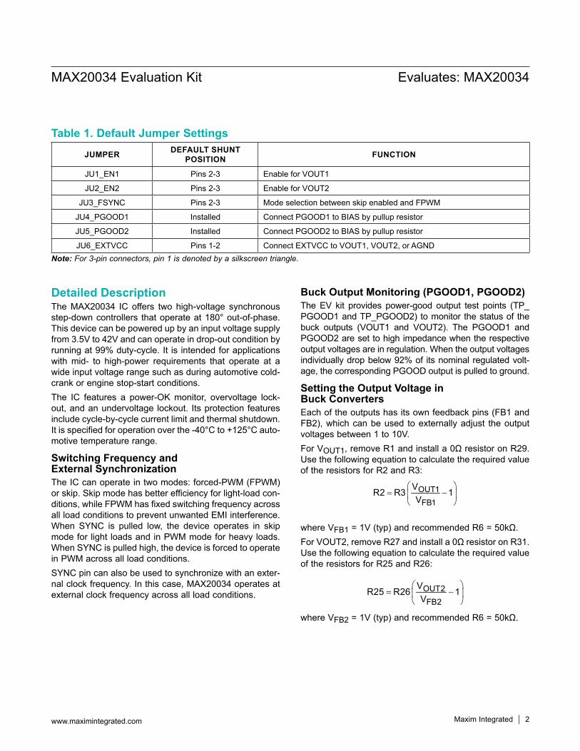
Table 1. Default Jumper SettingsJUMPER DEFAULT SHUNT
POSITION FUNCTION
JU1_EN1 Pins 2-3 Enable for VOUT1
JU2_EN2 Pins 2-3 Enable for VOUT2
JU3_FSYNC Pins 2-3 Mode selection between skip enabled and FPWM
JU4_PGOOD1 Installed Connect PGOOD1 to BIAS by pullup resistor
JU5_PGOOD2 Installed Connect PGOOD2 to BIAS by pullup resistor
JU6_EXTVCC Pins 1-2 Connect EXTVCC to VOUT1, VOUT2, or AGNDNote: For 3-pin connectors, pin 1 is denoted by a silkscreen triangle.

Maxim Integrated 3www.maximintegrated.com
Evaluates: MAX20034MAX20034 Evaluation Kit
Evaluate 400kHz or 2.2MHz OperationOrder MAX20034HFEVKIT# to evaluate 2.2MHz operation. Order MAX20034EVKIT# to evaluate 400kHz operation. Table 2 lists different component selections for 2.2MHz and 400kHz switching frequency (the other components remain the same).
Table 2. Component Selections
#Denotes RoHS compliant.
COMPONENT fSW = 2.2MHz fSW = 400kHzC10/C28 820pF 1500pF
C12/C26 2pF 2pF
L1/L3 2.2µH 4.7µH
R9/R20 51.1kΩ 24.9kΩ
R19 12kΩ 73.2kΩ
Ordering InformationPART TYPE fSW
MAX20034EVKIT# EV Kit 400kHzMAX20034HFEVKIT# EV Kit 2.2MHz

Maxim Integrated 4www.maximintegrated.com
Evaluates: MAX20034MAX20034 Evaluation Kit
MAX20034 EV Kit Bill of MaterialsPART QTY DESCRIPTION MFG PART #
C1, C2, C30, C32 4 CAPACITOR; SMT (1210); CERAMIC; 47UF; 10V; TOL=10%; MODEL=GRM SERIES; TG=-55 DEGC TO +125 DEGC; TC=X7R MURATA, GRM32ER71A476KE15
C3, C5, C29, C31, C37-C40 8 CAPACITOR; SMT (0402); CERAMIC CHIP; 100PF; 50V; TOL=2%; TG=-55 DEGC TO +125 DEGC; TC=C0G TDK, C1005C0G1H101G050
C4, C33 2 CAPACITOR; SMT (1210); CERAMIC; 47UF; 10V; TOL=10%; MODEL=GRM SERIES; TG=-55 DEGC TO +125 DEGC; TC=X7R MURATA, GRM32ER71A476KE15
C6, C7, C20, C35, C36 5 CAPACITOR; SMT (1206); CERAMIC CHIP; 4.7UF ; 50V; TOL=10%; TG=-55 DEGC TO +125 DEGC; TC=X7R; AUTO TDK, CGA5L3X7R1H475K160AB
C8, C13, C23, C34 4 CAPACITOR; SMT (0402); CERAMIC CHIP; 0.1UF; 50V; TOL=10%; TG=-55 DEGC TO +125 DEGC; TC=X7R TDK, CGA2B3X7R1H104K; C1005X7R1H104K050BB
C10, C28 2 CAPACITOR; SMT (0402); CERAMIC CHIP; 820PF; 50V; TOL=2%; TG=-55 DEGC TO +125 DEGC; TC=C0G MURATA, GRM1555C1H821GA01
C11, C16 2 CAPACITOR; SMT (1210); CERAMIC CHIP; 4.7UF; 50V; TOL=10%; TG=-55 DEGC TO +125 DEGC; TC=X7R; AUTO TDK, CGA6P3X7R1H475K
C12, C26 2 CAPACITOR; SMT (0402); CERAMIC CHIP; 2PF; 50V; TOL=0.1PF; TG=-55 DEGC TO +125 DEGC; TC=C0G TDK, C1005C0G1H020B050
C17 1 CAPACITOR; SMT (CASE_D); ALUMINUM-ELECTROLYTIC; 47UF; 50V; TOL=20%; TG=-55 DEGC TO +105 DEGC; AUTO PANASONIC, EEE-FT1H470AP
C18 1 CAPACITOR; SMT (1206); CERAMIC CHIP; 6.8UF; 16V; TOL=10%; TG=-55 DEGC TO +125 DEGC; TC=X7R TDK, C1206C685K4RAC; C3216X7R1C685K160AC
C21 1 CAPACITOR; SMT (0603); CERAMIC CHIP; 2.2UF; 10V; TOL=10%; TG=-55 DEGC TO +125 DEGC; TC=X7R MURATA, GRM188R71A225KE15; CL10B225KP8NNN
D2, D3 2 DIODE; SCH; SCHOTTKY DIODE; SMT (SOD-323); PIV=30V; IF=0.2A ON SEMICONDUCTOR, BAT54H
JU1_EN1, JU2_EN2, JU3_FSYNC 3 CONNECTOR; THROUGH HOLE; TSW SERIES; SINGLE ROW; STRAIGHT; 3PINS SAMTEC, TSW-103-07-T-S
JU4_PGOOD1, JU5_PGOOD2 2 CONNECTOR; THROUGH HOLE; TSW SERIES; SINGLE ROW; STRAIGHT; 2PINS; -55 DEGC TO +105 DEGC SAMTEC, TSW-102-07-T-S
JU6_EXTVCC 1 EVKIT PART-CONNECTOR; MALE; THROUGH HOLE; TSW SERIES; SINGLE ROW; STRAIGHT; 4PINS SAMTEC, TSW-104-07-L-S
L1, L3 2EVKIT PART-INDUCTOR; SMT; SHIELDED; 2.2UH; TOL=+/-20%; 12A; NOTE: ALTERNATE FOOTPRINT IS CAPABLE TO HOST IHLP-4040DZ-01; IHLP-2525CZ-L7 AND XAL50XX SERIES
VISHAY DALE, IHLP4040DZER2R2M01
L2 1 INDUCTOR; SMT (1206); FERRITE-BEAD; 1000; TOL=+/-25%; 1A FAIR-RITE, 2512061027Y1PGND, PGND1, PGND2, VBATT, VBATTF, VOUT1, VOUT2 7 EVK KIT PARTS; MAXIM PAD; NO WIRE TO BE SOLDERED ON THE
MAXIMPAD MAXIMPAD
Q1, Q2, Q3, Q4 4 TRAN; POWER MOSFET; SINGLE N-CHANNEL; NCH; SO-8FL; PD-(55W); I-(87A); V-(40V) ON SEMICONDUCTOR, NVMFS5C456NLT1G
R1, R6, R12, R13, R22, R27 6 RESISTOR; 0402; 0 OHM; 0%; JUMPER; 0.2W; THICK FILM VISHAY DALE, CRCW04020000Z0EDHPR2, R3, R7, R25, R26, R29, R31, R34 8 RESISTOR; 0402; 0 OHM; 0%; JUMPER; 0.2W; THICK FILM VISHAY DALE, CRCW04020000Z0EDHPR4, R24, R28, R30 4 RESISTOR; 0402; 20 OHM; 1%; 0.063W, THICK FILM VISHAY DALE, CRCW040220R0FKR5, R23 2 RESISTOR; 1206; 0.015 OHM; 1%; 100PPM; 0.5W; THICK FILM LRC-LRF1206LF-01-R015FR9, R14, R15, R20 4 RESISTOR; 0402; 51.1K OHM; 1%; 100PPM; 0.063W; THICK FILM VISHAY DALE, CRCW040251K1FKR10, R11, R17, R18 4 RESISTOR; 0603; 0 OHM; 0%; JUMPER; 0.1W; THICK FILM VISHAY DALE, CRCW06030000Z0R16 1 RESISTOR; 0402; 100K; 1%; 100PPM; 0.0625W; THICK FILM VISHAY DALE, CRCW0402100KFKR19 1 RESISTOR; 0402; 12.1K; 1%; 100PPM; 0.0625W; THICK FILM VISHAY DALE, CRCW040212K1FK
TP_FSYNC, TP_PGOOD1, TP_PGOOD2 3 TESTPOINT WITH 1.80MM HOLE DIA, RED, MULTIPURPOSE; NOT FOR COLD TEST KEYSTONE, 5010
U1 1EVKIT PART-IC; AUTOMOTIVE START-STOP POWER SUPPLY; QFN28-EP; PACKAGE CODE: T2855Y-5CMAX20034ATIR/VY+
MAX20034
— 1 PCB: MAX20034EVKIT MAX20034

Maxim Integrated 5www.maximintegrated.com
Evaluates: MAX20034MAX20034 Evaluation Kit
MAX20034 EV Kit Schematic
AGND
AGND
AGND
AGND
AGND
AGND
AGND
0402
0.1UF
VBAT
IHLP
4040
DZER
2R2M
01
2.2UH
820PF
0.015
00402
0402
0402
0402
OPEN
0.1UF
0402
0.015
1206
OPEN
47UF
1210
1210
0402
0402
OPEN
0
0402
0402
OPEN
47UF
1206
4.7UF
OPEN
1210
0402
OPEN
0402
OPEN
0
BIAS
VOUT2
0402
0402
BIAS
BIAS
0.1UF
1206
0402
OPEN
0OPEN
1206
4.7UF
0402
0603
0402
2.2UF
100K
BAT54H
0402
51.1K
51.1K
4.7UF
1206
4.7UF
1206
0OPEN
0402
0402
OPEN
OPEN
1210
47UF
1210
47UFVOUT1
0402
OPEN
0
VOUT2
0402
0.1UF
04020BAT54H
OPEN
0402
6.8UF
12.1K
04020
0
0603
BIAS
0603
MAX20034
Q1
5 123
5
4
Q3
5 123
Q4
5 123
U1
9
8
27
24
7
1619
28
23
21
26
25
29
10
17 15
14
11
1
22
20
12
13
R11
R10
C7C6
C8
R12D2A C
L1
12
R5
R2
R3
C3
R1
C18
C1C2
C4
VOUT
1
PGND
1
JU3_FSYNC
1
2
3
C21
R14
R15 2
TP_FSYNCR16
R19
R17
R18
L31
2
C29
R23
R25
C31
R26
R27C3
2
PGND
2
VOUT
2
C33
C30
C23
D3A C
R13
JU1_
EN1
1
2
3
2
3
PGND
R7
2
R6R2
2R3
4
C36
C34
R29
R31
3
C39
C40
BIAS
OPEN
VBAT
NVMFS5C456NLT1G
4
NVMFS5C456NLT1GC3
5
VBAT
JU2_
EN2
1
4
C13
4
2PF
4
Q2
0
2NVMFS5C456NLT1G
C12
BIAS
TP_PGOOD2
VBAT
C17
VBAT
TF
1210
C11
OPEN
1210
2
1
2OPEN
C16
OPEN
47UF
1
1VB
ATT
L2
4.7UF
1206C2
0
1 BIASJU5_PGOOD2
JU4_PGOOD1
0402
OPENC2
2
TP_PGOOD1
1
0402
C5
NVMFS5C456NLT1G
0603
1
C28820PF
2PF
OPEN
2VOUT1
JU6_
EXTV
CC
6R9
C10
0402
0402
20R4 20R28
0402
100PF
51.1K
0402
0402
C26
C38
100PF
0402
51.1K
R20
R30
20 0402
20
18
R24
0402
0402
432 5
C37
3
2.2UH
IHLP4040DZER2R2M01
LX1
EP
DH1
BST1
EN1
EN2
BST2
DH2
LX2
DL2
PGND
2
CS2
OUT
2
FB2
COM
P2
FOSC
FSYNC
PGOOD2
PGOOD1
IN
EXTVCC
AGND
BIAS
COM
P1
FB1
OUT
1
CS1
PGND
1
DL1
13
4 2
SD
G
SD
G
SD
G
SD
G
+

Maxim Integrated 6www.maximintegrated.com
Evaluates: MAX20034MAX20034 Evaluation Kit
MAX20034 EV Kit PCB Layout—Top
MAX20034 EV Kit PCB Layout—Internal2
MAX20034 EV Kit PCB Layout—Bottom
MAX20034 EV Kit PCB Layout—Internal3
MAX20034 EV Kit PCB Layouts

Maxim Integrated 7www.maximintegrated.com
Evaluates: MAX20034MAX20034 Evaluation Kit
MAX20034 EV Kit Component Placement Guide—Top Silkscreen
MAX20034 EV Kit Component Placement Guide—Bottom Silkscreen
MAX20034 EV Kit PCB Layouts (continued)

Maxim Integrated cannot assume responsibility for use of any circuitry other than circuitry entirely embodied in a Maxim Integrated product. No circuit patent licenses are implied. Maxim Integrated reserves the right to change the circuitry and specifications without notice at any time.
Maxim Integrated and the Maxim Integrated logo are trademarks of Maxim Integrated Products, Inc. © 2017 Maxim Integrated Products, Inc. 8
Evaluates: MAX20034MAX20034 Evaluation Kit
Revision HistoryREVISIONNUMBER
REVISIONDATE DESCRIPTION PAGES
CHANGED
0 11/17 Initial release —
For pricing, delivery, and ordering information, please contact Maxim Direct at 1-888-629-4642, or visit Maxim Integrated’s website at www.maximintegrated.com.