
Preparation and properties of · PDF filePreparation and properties of nanomaterials A. Credi...
58
Preparation and properties of nanomaterials A. Credi Nanotecnologia Molecolare LS-FCM Università di Bologna
Transcript of Preparation and properties of · PDF filePreparation and properties of nanomaterials A. Credi...
Preparation and propertiesof nanomaterials
A. Credi Nanotecnologia Molecolare LS-FCM Università di Bologna

A nanostructured material (or nanomaterial) is defined as a solid material characterized by at least one dimension in the nanometer range
A variety of materials1 – 1000 nm (thickness)
Surfaces and thin films
Metals, semiconductors, magnetic materialsSeveral nm in the three dimensions
3-D structures (superlattices)
Metals, semiconductors, magnetic mater.Several nm2 – µm22-D arrays (of nanoparticles)
Zeolites, phosphates, etc.0.5 – 10 nm (pore diam.)
Nanoporous solids
Carbon, layered metal chalcogenides1 – 100 nm (diam.)Nanotubes
Metals, semiconductors, oxides, sulfides, nitrides
1 – 100 nm (diam.)Nanowires
Ceramic oxides1 – 100 nm (diam.)Other nanoparticles
Metals, semiconductors, magnetic materials1 – 10 nm(diam.)
Nanocrystals and clusters(quantum dots)
MaterialsSize (approx.)
MOLECULES
BULK MATERIALS
A. Credi Nanotecnologia Molecolare LS-FCM Università di Bologna
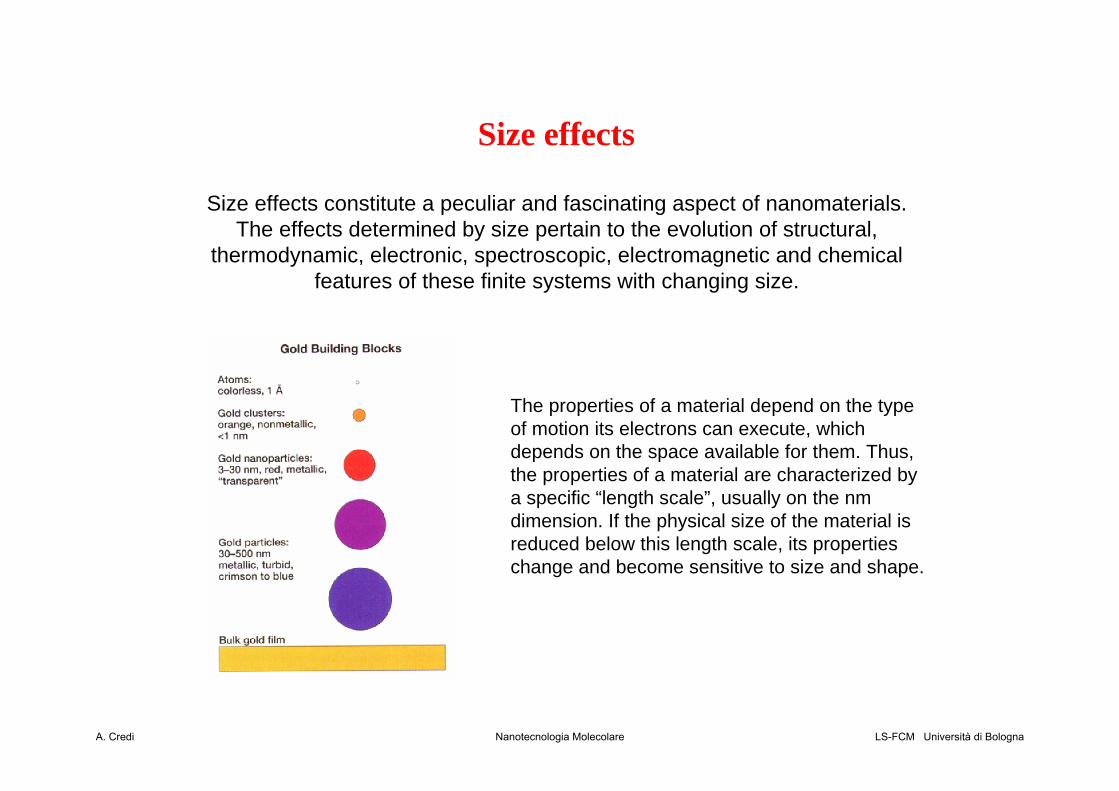
Size effects
Size effects constitute a peculiar and fascinating aspect of nanomaterials. The effects determined by size pertain to the evolution of structural,
thermodynamic, electronic, spectroscopic, electromagnetic and chemical features of these finite systems with changing size.
The properties of a material depend on the typeof motion its electrons can execute, whichdepends on the space available for them. Thus, the properties of a material are characterized bya specific “length scale”, usually on the nmdimension. If the physical size of the material isreduced below this length scale, its propertieschange and become sensitive to size and shape.
A. Credi Nanotecnologia Molecolare LS-FCM Università di Bologna

Size effects
Figure 48. Observation of discrete electronic transitions in optical absorption for a series of sizes of monodisperse CdSe.
Figure 4. Melting temperature versus size for CdS nanocrystals.
Figure 6. Size dependence of the wurtzite to rock salt pressure-induced structural transformation in CdSe nanocrystals.
A. Credi Nanotecnologia Molecolare LS-FCM Università di Bologna

Quantum confinement
In small nanocrystals, the electronic energy levels are not continuous asin the bulk but are discrete (finite density of states), because of the
confinement of the electronic wavefunction to the physical dimensions of the particles. This phenomenon is called quantum confinement and therefore nanocrystals are also referred to as quantum dots (QDs).
In any material, substantial variation of fundamental electrical and opticalproperties with reduced size will be observed when the energy spacing
between the electronic levels exceeds the thermal energy (kT).
Moreover, nanocrystals possess a high surface are and a large fractionof the atoms in a nanocrystal are on its surface. Since this fraction
depends largely on the size of the particle (30% for a 1-nm crystal, 15% for a 10-nm crystal), it can give rise to size effects in chemical and
physical properties of the nanocrystal.
A. Credi Nanotecnologia Molecolare LS-FCM Università di Bologna

Quantum confinement
Fig. 1.3. A plot of the average electronic energy level spacing (Kubo gap, δ) of sodium as a function of the particle diameter. Also shown is the percentage of Na atoms at the surface as
a function of particle diameter
NANOSCALE MICROSCALE
10-4
108
104
1
0.1 1 10 100 1000
0.001%
0.01%
0.1%
1%
10%
100%
Kubo
gap
(K)
Frac
tion
of a
tom
s on
sur
face
Particle diameter (nm)
A. Credi Nanotecnologia Molecolare LS-FCM Università di Bologna

Electronic band theory
Ener
gy
↑↓
↑ ↑ ↑ ↑ ↑ ↑
↑↓ ↑↓
↑↓↑ ↑ ↑ ↑
Biatomic molecule Li2 Triatomic molecule Li3 Tetratomic molecule Li4
2Li 2s1 3Li 2s1 4Li 2s1
σ
σ*
σ
σ*
σn
σ1
σ* 2
σ2
σ*1
NA Li 2s1
MO formetallic Lithium
NA Li½NA MO unoccupied
½NA MO occupied
A. Credi Nanotecnologia Molecolare LS-FCM Università di Bologna

Ener
gy
MO occupied
MO unoccup.
3s Band
FERMI LEVEL
Fermi level: in an orbital band electronic structure, it is the highest occupied electronic level
Electronic band theory
A. Credi Nanotecnologia Molecolare LS-FCM Università di Bologna
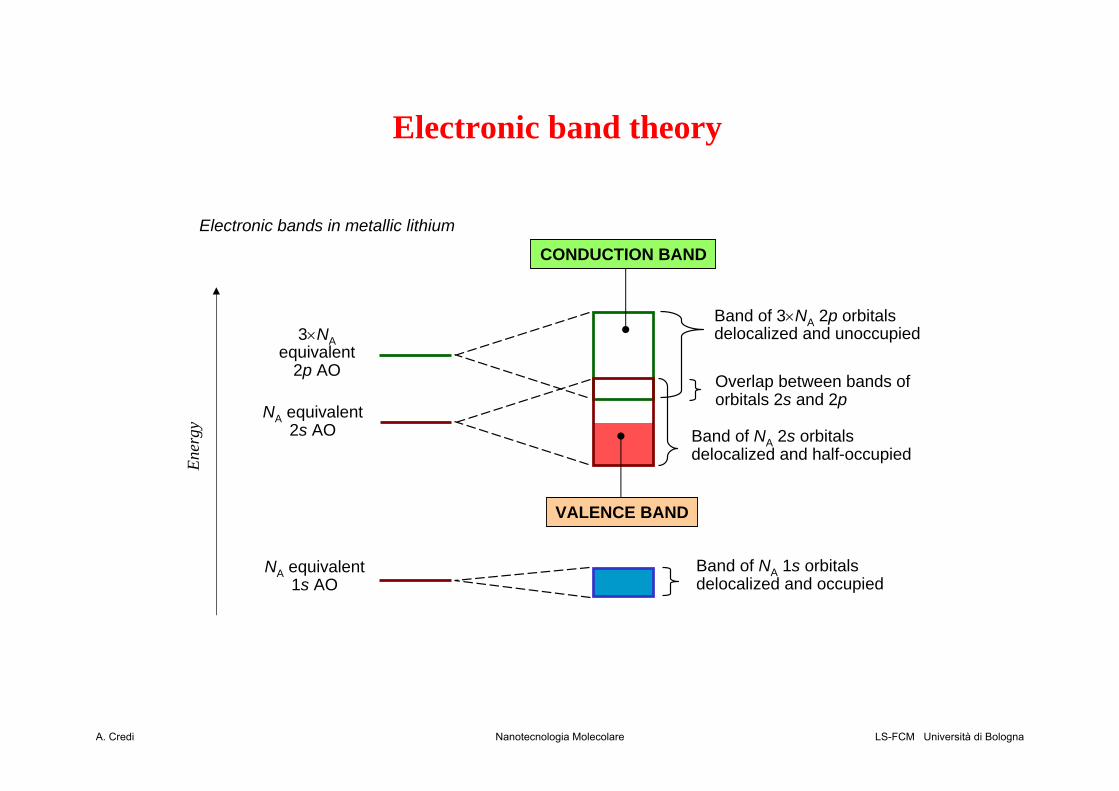
3×NAequivalent
2p AO
NA equivalent2s AO
NA equivalent1s AO
Ener
gy
Band of 3×NA 2p orbitalsdelocalized and unoccupied
Band of NA 2s orbitalsdelocalized and half-occupied
Overlap between bands of orbitals 2s and 2p
Band of NA 1s orbitalsdelocalized and occupied
Electronic bands in metallic lithium
VALENCE BAND
CONDUCTION BAND
Electronic band theory
A. Credi Nanotecnologia Molecolare LS-FCM Università di Bologna

Conductionband
(empty)
Valenceband(full)
Metal (conductor) Insulator Semiconductor
band gap band gap
Electronic band theory
A. Credi Nanotecnologia Molecolare LS-FCM Università di Bologna
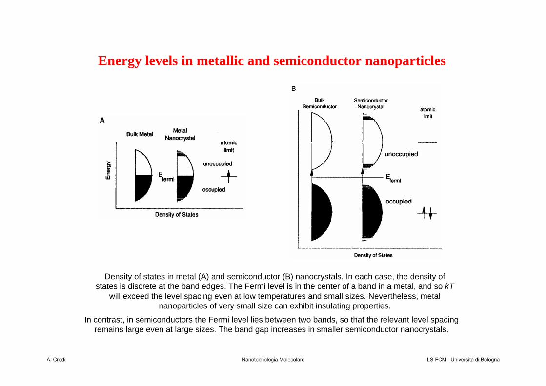
Energy levels in metallic and semiconductor nanoparticles
Density of states in metal (A) and semiconductor (B) nanocrystals. In each case, the density of states is discrete at the band edges. The Fermi level is in the center of a band in a metal, and so kT
will exceed the level spacing even at low temperatures and small sizes. Nevertheless, metal nanoparticles of very small size can exhibit insulating properties.
In contrast, in semiconductors the Fermi level lies between two bands, so that the relevant level spacingremains large even at large sizes. The band gap increases in smaller semiconductor nanocrystals.
A. Credi Nanotecnologia Molecolare LS-FCM Università di Bologna

Gold nanoparticles
5th Millennium B.C.: start of extraction of gold metal
Ca. 400 B.C.: appearance of “soluble” gold
Colloidal gold is still used for colouring and decorationpurposes
Gold nanoparticles are the most stable and widely used metal nanoparticles
the Lycurgus Cup (4th Century B.C) is rubyred in transmitted light and green in reflected
light, due to the presence of gold colloids
Gold colloids were used for aesthetic(decoration) and curative purposes
1857: Faraday reported formation of deep-red solutions of colloidal Au by reduction of anaqueous solution of AuCl4– by phosphorus in CS2 (two phase system)
Thin films prepared from dried colloidal solutions showed reversible colour changes uponmechanical compression.
A. Credi Nanotecnologia Molecolare LS-FCM Università di Bologna

Preparation of Au NP
All chemical methods for the preparation of gold nanoparticles are based on reduction of Au(III) derivatives. However, in general it is difficult to control the size of the nanoparticles, and in absence of stabilizing agents the particles tend to aggregate (collapse).
Alkylammonium salts can be used to stabilize nanoparticles, as they form a sort of “electricaldouble layer” on the surface. Such an interaction is weak and the gold surface remains reactive. For this reason, these nanoparticles are not very stable and cannot be separated from the solution from which they have been prepared.
The synthesis is usually performed in a two phase (water/organic solvent) system. Alkylammonium salts like TOAB (tetraoctylammonium bromide), besides passivating the gold surface, perform the task of phase transfer agents towards the Au(III) species to the organicphase.
A. Credi Nanotecnologia Molecolare LS-FCM Università di Bologna

Procedure for preparation of Au nanoparticles in a biphasic system.A phase-transfer agent which also acts as a surface stabilizer is employed.
TOAB=tetraoctylammonium bromide
HAuClWater
4
TOABToluene Stirring
Stirring
HAuClWater
4
NaBHWater
4
NaBH4Water
Au NPToluene
Water
Water
TOABToluene
TOA [AuCl ]Toluene
+4
_
TOA [AuCl ]Toluene
+4
_
TOA [AuCl ]Toluene
+4
_
Separation
Preparation of Au NP
A. Credi Nanotecnologia Molecolare LS-FCM Università di Bologna

Au nanoparticles, as well as other metal and metal oxide nanoparticles, can be prepared inside a suitable block copolymer micelle. Reduction of the metal salt is performed with usual reagents(H2, NaBH4, hydrazine)
Preparation of Au NP
A. Credi Nanotecnologia Molecolare LS-FCM Università di Bologna

HAuClWater
4
TOABToluene Stirring
Separation
NaBH4
Stirring
HAuClWater
4
R(CH ) SH2 n
Water
TOABToluene
TOA [AuCl ]Toluene
+4
_
TOA [AuCl ]Toluene
+4
_
Au RS
R
S
R
SR
S
R
S
R
SR S
R
S
R
SR
S
R
S
R
S
TOAB=tetraoctyl-ammonium bromide
M. Brust et al., J. Chem. Soc. Chem. Commun. 1994, 801; 1995, 1655.
Formation of Au NP coated withorganic shells by reduction of Au(III) compounds in the presence of thiols
Preparation of Au NP: the Brust-Schiffrin method
A. Credi Nanotecnologia Molecolare LS-FCM Università di Bologna

Au clusters and NP
TEM images and size distributions of Au NP capped withdodecanethiol: (b) as prepared and after heating at (c) 150°C, (d) 190°C, (e) 230°C. (f): octadecanethiol Au NP heat-treated at 250°C
The size of the NP can be controlled from the stoichiometric ratio of the reactants employed in the synthesis. For example, the following ratios
HAuCl4 : TOAB : thiol : NaBH4 = 1 : 3 : 2 : 10
afford NP of diameter around 5 nm.
Gold clusters are made up of a defined number of Auatoms. Such a number is based on the dense packing of atoms taken as spheres, each atom beingsurrounded by 12 nearest neighbors. Thus, the smallest cluster contains 13 atoms, and the followinglayers contain 10n2+2 atoms (n = layer number). Clusters containing 55, 147, 309, 561, 923, 1415 and up to 2057 atoms (n=2–8) have been isolated.
Larger aggregates constitute the fuzzy frontierbetween clusters and colloids (Au NP), the latterbeing objects with some dispersity described by a histogram of size distribution determined using TEM data.
A. Credi Nanotecnologia Molecolare LS-FCM Università di Bologna

Optical properties of metal NP
The optical properties of metallic NP are determinedby the surface plasmon resonance phenomenon. The SPR is caused by the coherent motion of the conduction band electrons from one surface of the particle to the other, upon interaction with anelectromagnetic field.The decrease in size below the electron mean free path (distance the electron travels between scattering collisions with the lattice centers) gives rise to intense absorption in the UV-vis range. Optical excitation of the SPR gives rise to the surface plasmonabsorption
UV-vis absorption spectra of (a) AuCl4–, and Au NP capped with dodecanethiol with the following
mean size: (b) 1.5, (c) 3.4, (d) 5.4, (e) 6.8 nm.
57599
53348
52122
52015
5179
no SPA band<2
SPA λmax (nm)d (nm)
λmax of SPA for Au NP in water
Figure 59. Illustration of the excitation of the dipole surface plasmonoscillation. A dipolar oscillation of the electrons is created with period T
Figure 60. Optical absorption spectra of 22, 48, and 99nm spherical gold nanoparticles. The broad absorptionband corresponds to the surface plasmon resonance.
For Ag NP, the SPR band peaks around 370 nm
A. Credi Nanotecnologia Molecolare LS-FCM Università di Bologna

Optical properties of metal NP
The surface plasmon absorption depends on the size and the shape of the particles, and on the dielectric constant of the matrix. For small particles it depends also on the nature of the
molecules adsorbed on the NP surface.
A. Credi Nanotecnologia Molecolare LS-FCM Università di Bologna
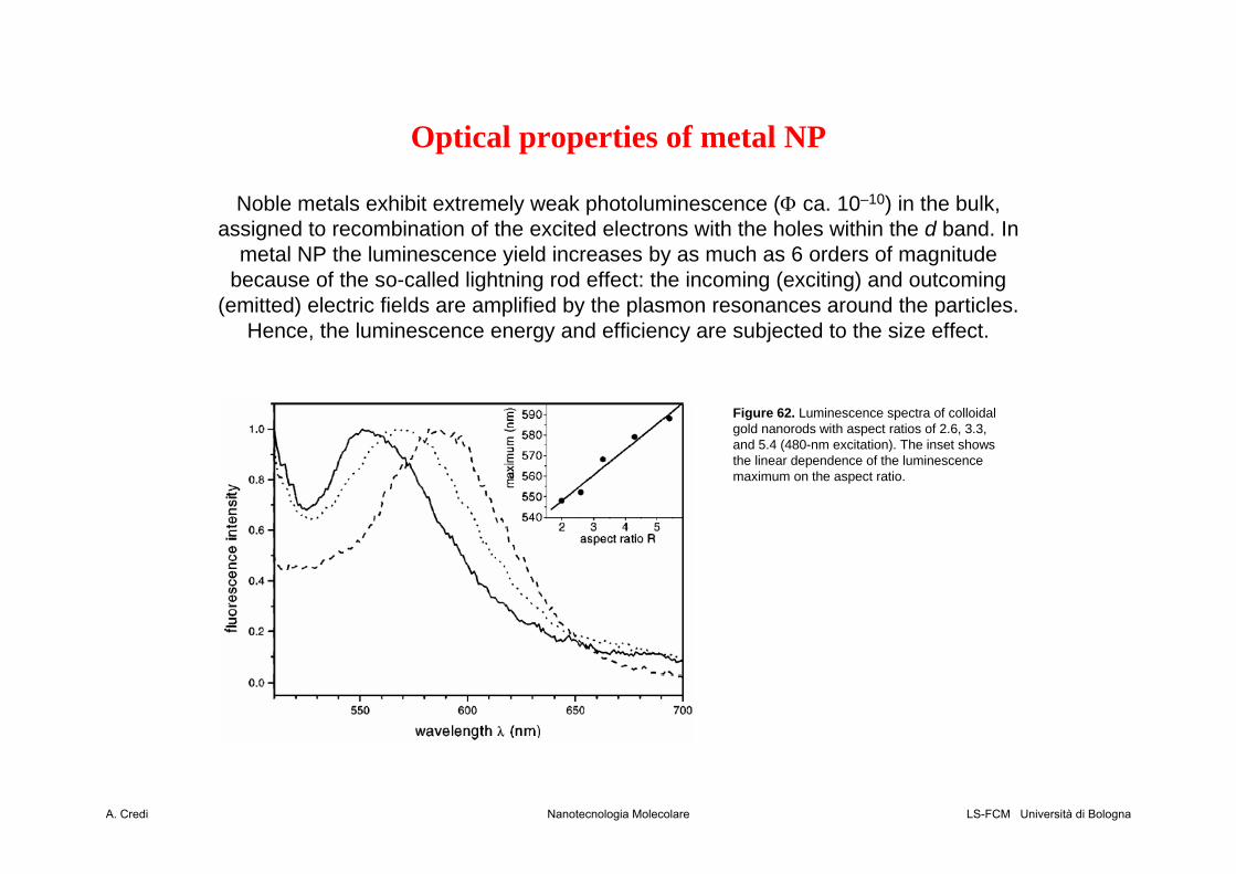
Optical properties of metal NP
Noble metals exhibit extremely weak photoluminescence (Φ ca. 10–10) in the bulk, assigned to recombination of the excited electrons with the holes within the d band. In
metal NP the luminescence yield increases by as much as 6 orders of magnitude because of the so-called lightning rod effect: the incoming (exciting) and outcoming
(emitted) electric fields are amplified by the plasmon resonances around the particles. Hence, the luminescence energy and efficiency are subjected to the size effect.
Figure 62. Luminescence spectra of colloidal gold nanorods with aspect ratios of 2.6, 3.3, and 5.4 (480-nm excitation). The inset showsthe linear dependence of the luminescencemaximum on the aspect ratio.
A. Credi Nanotecnologia Molecolare LS-FCM Università di Bologna

Electrical properties of metal NPElectrical conductivity of bulk metals is based on their electronic band structures, and the mobility of
electrons is related to their mean free path between two collisions with the lattice. The collectivemotion of electrons in a bulk metal obeys Ohm’s law, V = RI, where V is the applied voltage, R is
the resistance of the material and I is the current.
As the electronic band structure changes intodiscrete energy levels, Ohm’s law is no longervalid. If one electron is transferred to a smallparticle, the Coulomb energy of the latterincreases by EC = e2/2C, where C is the capacitance of the particle. If the temperature islow such that kT < e2/2C, single electron tunneling processes are observed.*
* Thermal motion of the atoms in the particle can initiate a change in the charge and the Coulomb energy so that further electrons may tunnel uncontrolled
Hence, the I-V characteristic of a quantum dotis not linear, but staircase-like. No currentflows up to VC = ±e/2C. If this value is reached, an electron can be transferred. Following this, an electron tunnelling process occurs if the Coulomb energy of the particle is compensated by an external voltage of V = ±ne/2C. This behaviour is called Coulomb blockade. The charging energy increases with decreasing the size of the quantum dot.
Figure 66. I-U characteristic of ideal single electron transport, where Coulomb blockade is shown as the step function.
A. Credi Nanotecnologia Molecolare LS-FCM Università di Bologna

Electrical properties of metal NP
Fig. 1.7. (a) I–V characteristic of an isolated 3.3 nm Pd nanocrystal (dotted line) and the theoretical fit (solid line) obtained at 300 K using a semiclassical model. (b) The size dependence of the charging energy. (Experimental setup as in Fig. 1)
Figure 67. (a) Field emission scanning electron micrograph of a leadstructure before the nanocrystals are introduced. The light gray region is formed by the angle evaporation and is 10 nm thick. The darker region isfrom a normal angle evaporation and is 70 nm thick. (b) Schematic cross section of nanocrystals bound via a bifunctional linker molecule to the leads. Transport between the leads occurs through the mottled nanocrystal bridging the gap.
a)
b)
Fig. 1. Schematic illustrationof a single-electron tunnel junction formed by a nanocrystal held betweenthe STM tip and the substrate.
Experimental approaches to measure the Coulomb blockade.
Two metallic leads with spacing of a few nm are fabricated. An organicmonolayer is then used to bind nanocrystals to the leads. When a nanocrystalbridges the gap between the leads, it can be electrically investigated.
A. Credi Nanotecnologia Molecolare LS-FCM Università di Bologna
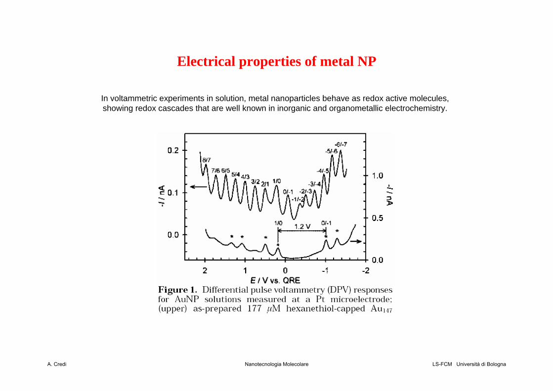
Electrical properties of metal NP
In voltammetric experiments in solution, metal nanoparticles behave as redox active molecules, showing redox cascades that are well known in inorganic and organometallic electrochemistry.
A. Credi Nanotecnologia Molecolare LS-FCM Università di Bologna

Preparation of semiconductor nanoparticlesThe chemical growth of bulk or nanometer-sized materials involves the process of precipitation of a solid phase from solution. The challenge in nanoparticles synthesis is to control the size and shape
of the crystals such that their properties can be tailored. This requires the understanding and control of the key processes of nucleation, growth and termination.
Many strategies are available: sol processes, micelles, sol-gel, hydrothermal syntheses, etc.
Among the most common and widely studied semiconductor nanoparticles are those of the II-VI type (ZnS, ZnSe, CdS, CdSe, CdTe and HgS) and of the III-V type (e.g., GaAs, InP and InAs)
Semiconductor NP can be prepared in aqueous media using stabilizing agents, with proceduressimilar to those employed for the synthesis of gold NP. These approaches, however, lead to highly
defective and polydisperse nanocrystals. More recently, procedures have been reported for the synthesis of highly crystalline and nearly monodisperse NP. E.g., for CdE (E=S, Se or Te):
Cd precursor (dimethyl Cd, Cd oxide, carbonate or acetate) +
chalcogen (elemental S, Se or Te) in a hot coordinating solvent (e.g., TOPO, tri-n-octylphosphine oxide)
High temperature(fast particlenucleation)
Low temperature(slow particle
growth)
Desired sizereached?
ReactionquenchingWashingNanoparticles YES NO
A. Credi Nanotecnologia Molecolare LS-FCM Università di Bologna

Optical properties of semiconductor NP
Ene
rgy
Bandgap
VB
CB
VB
CB_
+
hν' Band edgeluminescence
hν > b.g.
VB
CB _
+
electron-hole pair(exciton)
thermalrelaxation
In semiconductors, optical excitation causes the promotion of a valence band electron into the conduction band, leaving behind a valence band hole. Once promotion has occurred, the CB
electron quickly relaxes into the lowest energy CB state, while the hole moves to the top of the VB (VB electrons cascade down into lower energy valence states). The coupled electron-hole pair is
often referred to as a single entity called exciton, since one cannot exist without the other.
Photoluminescence arises from recombination of the CB electron with the VB hole and is calledband edge luminescence. Such a luminescence is characterized by a very small Stokes shift
relative to band edge absorption.
A. Credi Nanotecnologia Molecolare LS-FCM Università di Bologna
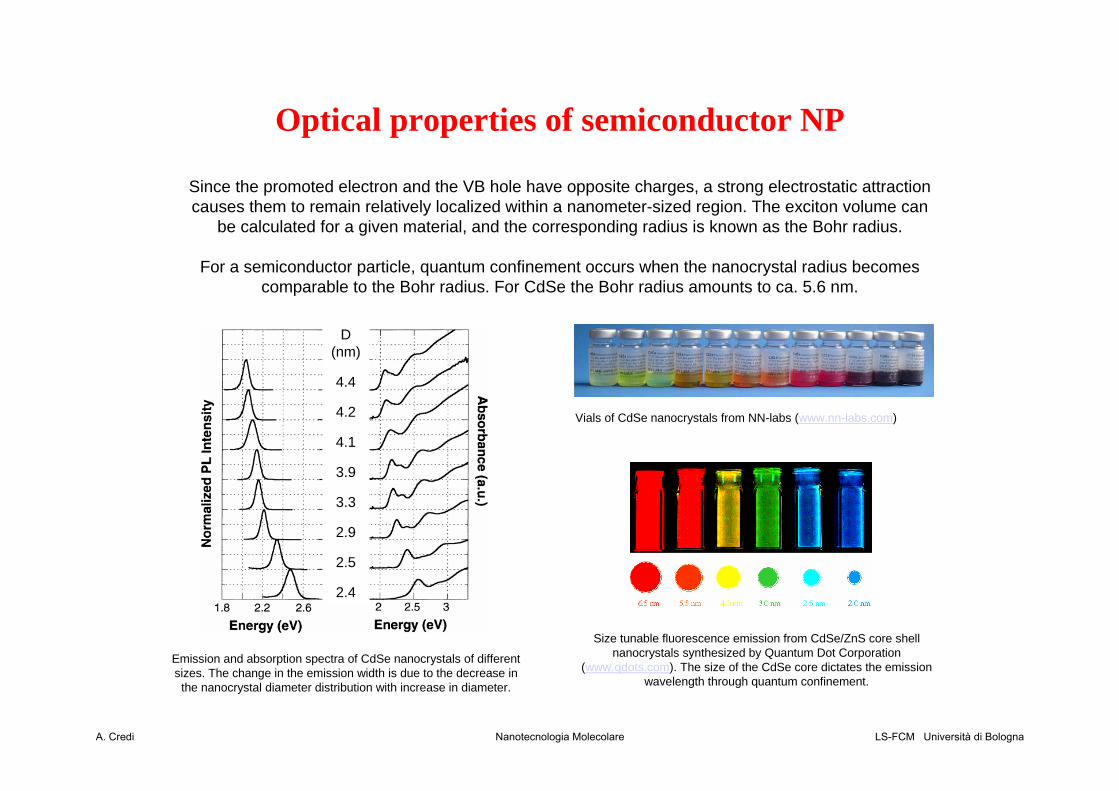
Optical properties of semiconductor NP
Since the promoted electron and the VB hole have opposite charges, a strong electrostatic attractioncauses them to remain relatively localized within a nanometer-sized region. The exciton volume can
be calculated for a given material, and the corresponding radius is known as the Bohr radius.
For a semiconductor particle, quantum confinement occurs when the nanocrystal radius becomescomparable to the Bohr radius. For CdSe the Bohr radius amounts to ca. 5.6 nm.
Emission and absorption spectra of CdSe nanocrystals of differentsizes. The change in the emission width is due to the decrease in
the nanocrystal diameter distribution with increase in diameter.
D(nm)
4.4
4.2
4.1
3.9
3.3
2.9
2.5
2.4
Size tunable fluorescence emission from CdSe/ZnS core shell nanocrystals synthesized by Quantum Dot Corporation
(www.qdots.com). The size of the CdSe core dictates the emission wavelength through quantum confinement.
Vials of CdSe nanocrystals from NN-labs (www.nn-labs.com)
A. Credi Nanotecnologia Molecolare LS-FCM Università di Bologna

Optical properties of semiconductor NPThe presence of dangling orbitals at the surface of the NP, or any defect states in the bulk, provide traps for the excited electrons and holes prior to recombination. Therefore, an electron excited to the CB, or a VB hole, can
transfer itself non-radiatively to one of these surface or defect states before undergoing a (radiative or non-radiative) transition to a lower energy state. The net result is that either band edge luminescence is quenched, or emission is
shifted to much lower energies compared to those of band edge recombination (redshifted emission of NP)
Band edge emission: small stokes shift, sharp, controllable by sizeDefect (redshifted) emission: large stokes shift, broad,
controllable by chemical means (doping)
A. Credi Nanotecnologia Molecolare LS-FCM Università di Bologna

Optical properties of semiconductor NPSince defect emission is difficult to fine tune, for many applications it is important to preserve band
edge emission. To this aim, the surface of the NP can be passivated by chemically binding a capping agent. Another approach consists in overcoating a nanocrystal of a given semiconductor
with a thin layer of a semiconductor with higher band gap (core-shell particles).
All semiconductors undergo absorption processes, but because of selection rules (conservation of momentum) only direct gap semiconductors (e.g. CdSe) exhibit intense band edge luminescence, with yields close to 100%. Indirect gap semiconductors (e.g. Si) show luminescence with yields that are 3 to 4 orders of magnitude smallerthan direct gap materials.
A. Credi Nanotecnologia Molecolare LS-FCM Università di Bologna

Engineered semiconductor NP for NIR LEDs
Science 2002, 295, 1506-1508
Core: InAs (2.4 nm diameter)Shell: ZnSe (1.5 monolayers)
MEHPPV/NC compositesSpin-casted films on glass or ITOThickness ca. 100 nm
A. Credi Nanotecnologia Molecolare LS-FCM Università di Bologna
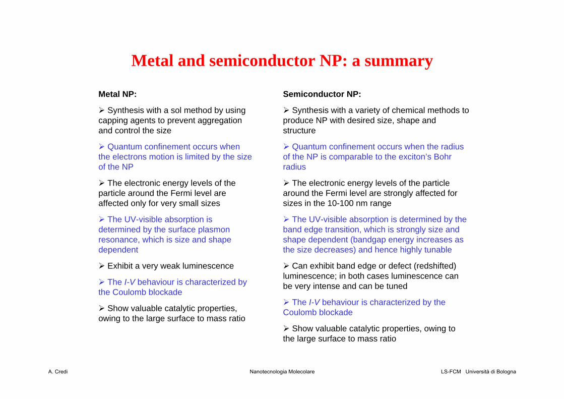
Metal and semiconductor NP: a summary
Metal NP:
Synthesis with a sol method by usingcapping agents to prevent aggregationand control the size
Quantum confinement occurs when the electrons motion is limited by the size of the NP
The electronic energy levels of the particle around the Fermi level are affected only for very small sizes
The UV-visible absorption isdetermined by the surface plasmon resonance, which is size and shapedependent
Exhibit a very weak luminescence
The I-V behaviour is characterized by the Coulomb blockade
Show valuable catalytic properties, owing to the large surface to mass ratio
Semiconductor NP:
Synthesis with a variety of chemical methods toproduce NP with desired size, shape and structure
Quantum confinement occurs when the radius of the NP is comparable to the exciton’s Bohr radius
The electronic energy levels of the particle around the Fermi level are strongly affected for sizes in the 10-100 nm range
The UV-visible absorption is determined by the band edge transition, which is strongly size and shape dependent (bandgap energy increases asthe size decreases) and hence highly tunable
Can exhibit band edge or defect (redshifted) luminescence; in both cases luminescence can be very intense and can be tuned
The I-V behaviour is characterized by the Coulomb blockade
Show valuable catalytic properties, owing to the large surface to mass ratio
A. Credi Nanotecnologia Molecolare LS-FCM Università di Bologna

Chemically functionalized nanoparticles
Au RS
R
S
R
SR
S
R
S
R
SR S
R
S
R
SR
S
R
S
R
S
A. Credi Nanotecnologia Molecolare LS-FCM Università di Bologna

Chemically functionalized nanoparticles:“Heterosupramolecular Chemistry”
When one (of more) component(s) of a supramolecular system is a condensed-phase component (referred to as a heterocomponent), a heterosupermolecule is formed.
The heterocomponent is usually a metal or metal oxide nanoparticle, and it is linked to the other molecular components by exploiting the same type of interactions used to prepare SAMs.
molecularcomponents
heterocomponent(nanoparticle)
heterosupramolecularsystem
self-assembly
A. Credi Nanotecnologia Molecolare LS-FCM Università di Bologna
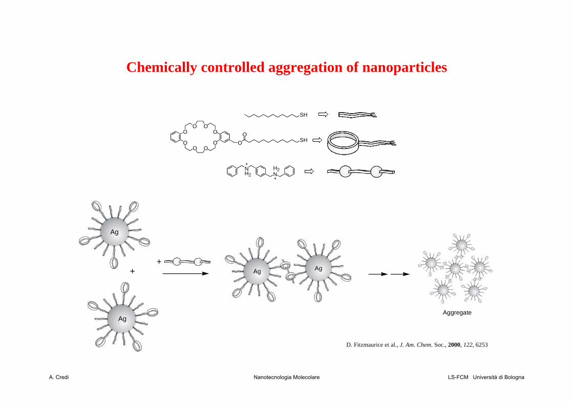
Chemically controlled aggregation of nanoparticles
SH
OOO
O
OO O
O O SHO
NH2
H2N
+
+
+
Ag
Ag
+Ag Ag
Aggregate
D. Fitzmaurice et al., J. Am. Chem. Soc., 2000, 122, 6253
A. Credi Nanotecnologia Molecolare LS-FCM Università di Bologna
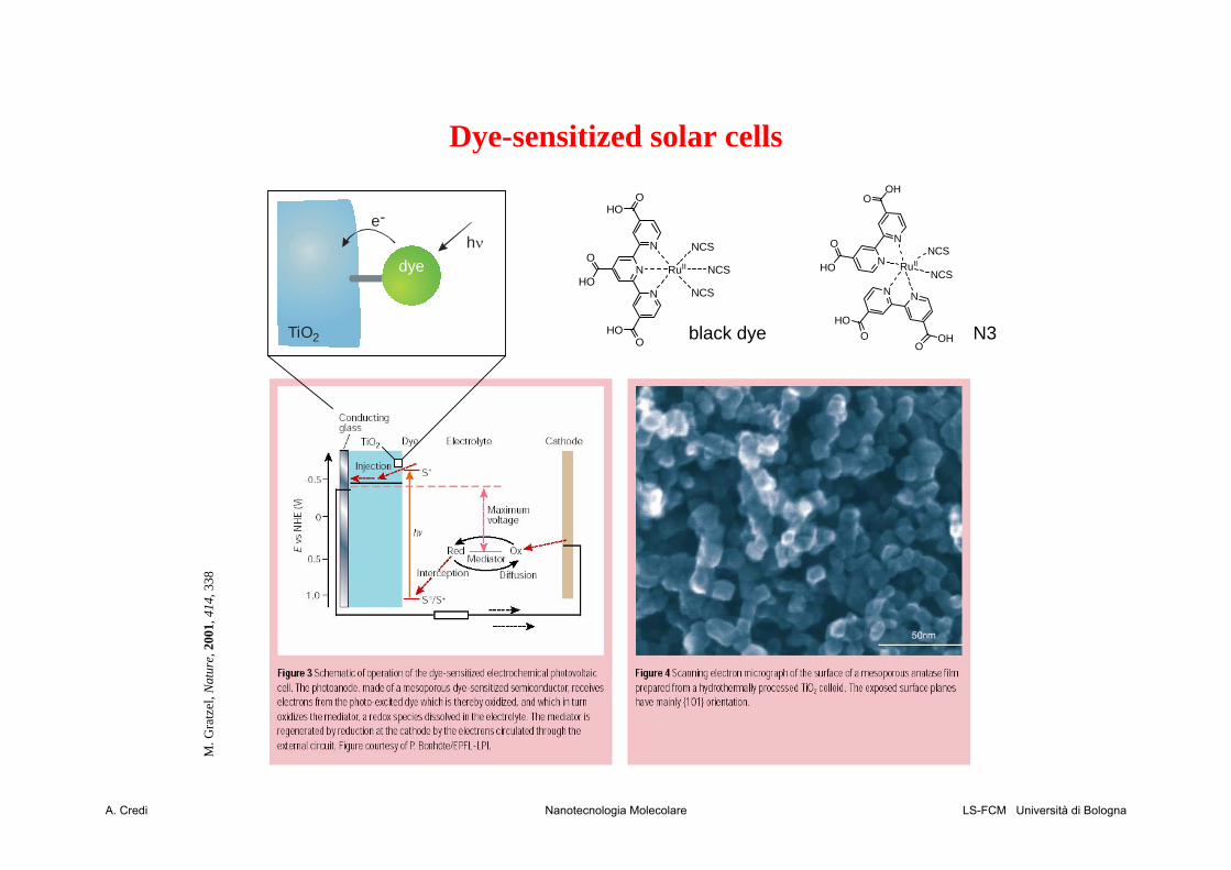
Dye-sensitized solar cells
M. G
ratz
el, N
atur
e, 2
001,
414
, 338
TiO2
dyehν
e-
N
N
N
O
HO
HOO
HOO
RuII
NCS
NCS
NCS
N
NHO
O
OHO
N N
OHO
HOO
RuIINCS
NCS
black dye N3
A. Credi Nanotecnologia Molecolare LS-FCM Università di Bologna
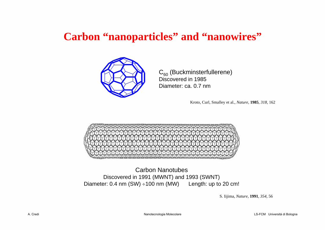
Carbon “nanoparticles” and “nanowires”
C60 (Buckminsterfullerene)Discovered in 1985Diameter: ca. 0.7 nm
Kroto, Curl, Smalley et al., Nature, 1985, 318, 162
Carbon NanotubesDiscovered in 1991 (MWNT) and 1993 (SWNT)
Diameter: 0.4 nm (SW) ÷100 nm (MW) Length: up to 20 cm!
S. Iijima, Nature, 1991, 354, 56
A. Credi Nanotecnologia Molecolare LS-FCM Università di Bologna

The fullerene family
C60 (Buckminsterfullerene)
Higherfullerenes
A. Credi Nanotecnologia Molecolare LS-FCM Università di Bologna

Preparation of fullerenes
• Graphite vaporization under high energy laser pulse in inert atmosphere, followed by ionization and mass spectrometry(Kroto, Smalley, Curl 1985)
• Electrical discharge between graphiteelectrodes in an atmosphere of He at 100 torr.The resulting soot is scraped from the evaporation chamber and dissolved in benzene.Further separation and purificationleads to C60 in gram scale(Kratshcmer, Huffman 1990)
• Cost: ~ 800 €/g (Aldrich)
A. Credi Nanotecnologia Molecolare LS-FCM Università di Bologna

• Structure: 20 hexagons and 12 pentagons, truncated icosahedron
• 60 atoms C sp2, perfectlyequivalent, a kind of …“huge atom”
6,61.38 Å
5,61.45 Å
Structural features of C60
Different reactivity!(6,6 > 5,6)
• Diameter of the inner cavity: 3.6 Å
Examples ofendohedralfullerenes:N@C60, Li@C60,He@C60, Ln@C60,Ln@C70, Ln@C82
A. Credi Nanotecnologia Molecolare LS-FCM Università di Bologna
Properties of C60 and its derivatives
• Black crystalline solid, thermally stable up to 400 °C
• Doped with alkali metals: conductor and superconductor
• Very difficult to oxidize
• Easy to reduce, six reversible stepwise reductions
• Only (sparingly) soluble in organic apolar solvents (CS2, benzene, toluene, CH2Cl2)
• Broad UV-vis absorption
• Long lived triplet excited state with high absorption coefficient
• Acceptors of electrons and electronic energy
• Photostable
• Potent singlet oxygen sensitizers
• Fluorescence
A. Credi Nanotecnologia Molecolare LS-FCM Università di Bologna

Change of electronic structure, change in colour
A. Credi Nanotecnologia Molecolare LS-FCM Università di Bologna
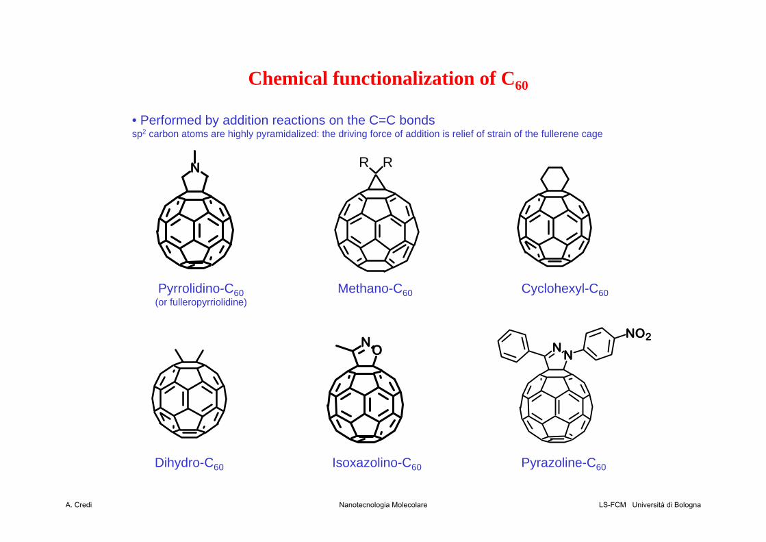
N R R
NO N
N
NO2
Pyrrolidino-C60(or fulleropyrriolidine)
Methano-C60 Cyclohexyl-C60
Dihydro-C60 Isoxazolino-C60 Pyrazoline-C60
Chemical functionalization of C60
• Performed by addition reactions on the C=C bondssp2 carbon atoms are highly pyramidalized: the driving force of addition is relief of strain of the fullerene cage
A. Credi Nanotecnologia Molecolare LS-FCM Università di Bologna
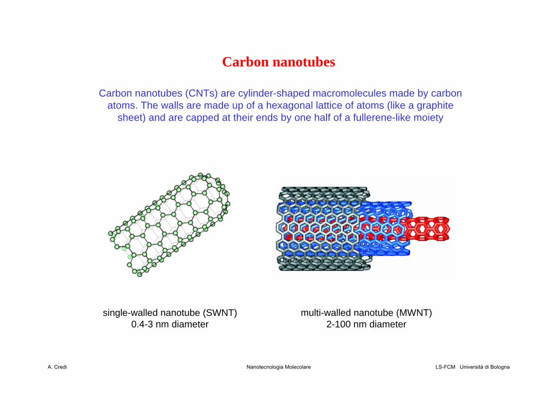
Carbon nanotubes
Carbon nanotubes (CNTs) are cylinder-shaped macromolecules made by carbonatoms. The walls are made up of a hexagonal lattice of atoms (like a graphite
sheet) and are capped at their ends by one half of a fullerene-like moiety
single-walled nanotube (SWNT)0.4-3 nm diameter
multi-walled nanotube (MWNT)2-100 nm diameter
A. Credi Nanotecnologia Molecolare LS-FCM Università di Bologna
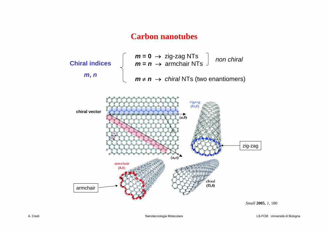
Carbon nanotubes
chiral vector
m = 0 → zig-zag NTsm = n → armchair NTs
m ≠ n → chiral NTs (two enantiomers)
non chiralChiral indices
m, n
Small 2005, 1, 180
zig-zag
armchair
A. Credi Nanotecnologia Molecolare LS-FCM Università di Bologna

Preparation of carbon nanotubes
Cost: ~ 100 €/g (but purity is very low)
A. Credi Nanotecnologia Molecolare LS-FCM Università di Bologna
Properties of carbon nanotubes
ELECTRICAL PROPERTIESThe main interest around CNTs arises from their electrical properties. Calculations, verified by single-molecule experiments, show that they are expected to be metallic or semiconducting depending on their structure, i.e. on their chiral vector• Armchair NTs show metallic properties• Zig-zag and chiral NTs can be either metallic or semiconducting
n – m = 3k (with k integer): metallic NTsn – m ≠ 3k: semiconducting NTs (Ebandgap ∝ diameter–1)
At present, no synthetic method ensures a reliable control of the electricalproperties of the NTs. The raw nanotube material thus consists of a mixture of metallic and semiconducting NTs (usually in ratio of 1:2). Separation of the metallic NTs from semiconductor ones is extremely difficult
MECHANICAL PROPERTIESCNTs possess highly valuable mechanical properties:• Tensile strength 10 times larger than a steel wire of corresponding diameter• Huge aspect ratio (length/diameter)• Low density (6 times smaller than that of steel)
Similarly shaped molecules consisting of only one element (carbon) may have verydifferent electronic behaviour!
A. Credi Nanotecnologia Molecolare LS-FCM Università di Bologna
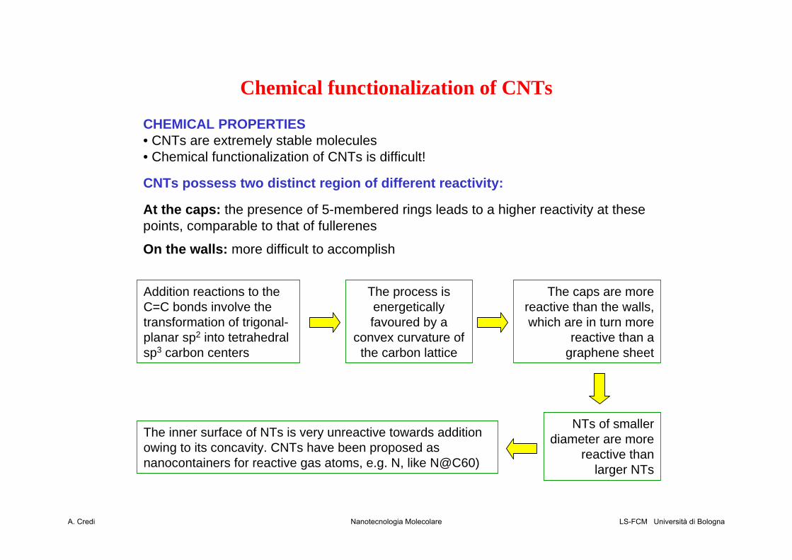
Chemical functionalization of CNTs
CNTs possess two distinct region of different reactivity:
At the caps: the presence of 5-membered rings leads to a higher reactivity at thesepoints, comparable to that of fullerenes
On the walls: more difficult to accomplish
Addition reactions to the C=C bonds involve the transformation of trigonal-planar sp2 into tetrahedralsp3 carbon centers
The process isenergeticallyfavoured by a
convex curvature of the carbon lattice
The caps are more reactive than the walls, which are in turn more
reactive than a graphene sheet
NTs of smallerdiameter are more
reactive thanlarger NTs
The inner surface of NTs is very unreactive towards additionowing to its concavity. CNTs have been proposed asnanocontainers for reactive gas atoms, e.g. N, like N@C60)
CHEMICAL PROPERTIES• CNTs are extremely stable molecules• Chemical functionalization of CNTs is difficult!
A. Credi Nanotecnologia Molecolare LS-FCM Università di Bologna

Chemical functionalization of CNTs
CNTs are not ideal structures: they contain defects formed during synthesisTypically 1–3% of the C atoms are located at a defect site
The Stone-Wales defect (two pairs of 5-membered and 7-membered rings, alsoknown as 7-5-5-7) is one of the most common defects. It leads to a local deformation
of the graphene sidewall, introducing an increased curvature (→ higher reactivity). The strongest curvature is at the border between the two 5-membered rings
A. Credi Nanotecnologia Molecolare LS-FCM Università di Bologna

Possible applications of CNTs
• Nanowires (metallic NTs)• Field-effect transistors (semiconductor NTs)• Chemical sensors (all atoms are on surface!)• Electrochemical sensors (high electron transfer rates for many redox couples and size comparable to biomolecules → NTs as nanoelectrodes)• Heterogeneous catalysis (defined morphology, covalent attachment of catalyst units)• Mechanically reinforced composites (e.g. with polymeric materials)
A. Credi Nanotecnologia Molecolare LS-FCM Università di Bologna
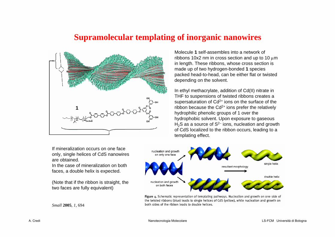
Supramolecular templating of inorganic nanowiresMolecule 1 self-assembles into a network of ribbons 10x2 nm in cross section and up to 10 μm in length. These ribbons, whose cross section ismade up of two hydrogen-bonded 1 speciespacked head-to-head, can be either flat or twisteddepending on the solvent.
1
In ethyl methacrylate, addition of Cd(II) nitrate in THF to suspensions of twisted ribbons creates a supersaturation of Cd2+ ions on the surface of the ribbon because the Cd2+ ions prefer the relativelyhydrophilic phenolic groups of 1 over the hydrophobic solvent. Upon exposure to gaseousH2S as a source of S2– ions, nucleation and growth of CdS localized to the ribbon occurs, leading to a templating effect.
If mineralization occurs on one face only, single helices of CdS nanowiresare obtained.In the case of mineralization on bothfaces, a double helix is expected.
(Note that if the ribbon is straight, the two faces are fully equivalent)
Small 2005, 1, 694
A. Credi Nanotecnologia Molecolare LS-FCM Università di Bologna

Supramolecular templating of inorganic nanowires
Formation of double vs single helices does not dependon mineralization time. Single helices are normallyobtained with freshly prepared ribbons, whereas doublehelices are formed by using aged ribbons → the different templating ability must reside in structuraldifferences between ribbons
A. Credi Nanotecnologia Molecolare LS-FCM Università di Bologna
Chem. Rev.2005, 105, 1445
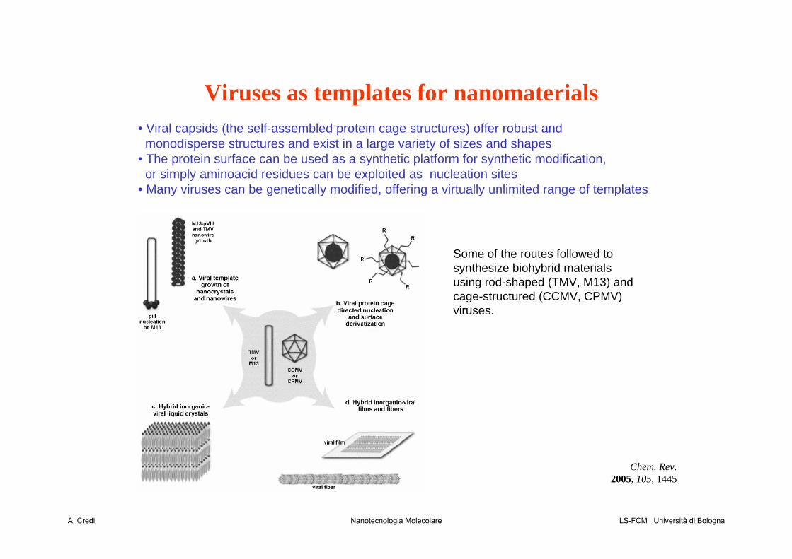
Viruses as templates for nanomaterials• Viral capsids (the self-assembled protein cage structures) offer robust andmonodisperse structures and exist in a large variety of sizes and shapes
• The protein surface can be used as a synthetic platform for synthetic modification,or simply aminoacid residues can be exploited as nucleation sites
• Many viruses can be genetically modified, offering a virtually unlimited range of templates
Some of the routes followed tosynthesize biohybrid materialsusing rod-shaped (TMV, M13) and cage-structured (CCMV, CPMV) viruses.
A. Credi Nanotecnologia Molecolare LS-FCM Università di Bologna

Chem. Rev.2005, 105, 1445
TMV template-directed synthesis of metallic nanowires
The metal crystals can bedeposited by electrochemicalmethods.
Depending on the metallizationconditions, it is possible selectivelytarget the outer or inner surface of the tubelike Tobacco Mosaic Virus
A. Credi Nanotecnologia Molecolare LS-FCM Università di Bologna

Chem. Rev. 2005, 105, 1445
M13 template-directed synthesis of nanowires
The M13 bacteriophage is a rod-shaped virus which infects bacteria. This virus contains a single stranded DNA and three different types of coat proteins. 2700 copies of the major coat protein are arranged in a repeating
helical array, forming a flexible cylinder in which the DNA is encased. Five copies of the two minor coat proteinsare situated at each end of the virus. The wild-type virus is approximately 860 nm long and 6.5 nm wide.
The viral coat proteins can be easily modified by genetic engineering to insert nucleation centers on the virus surface or to specifically functionalize viruses with different binding motifs.
A. Credi Nanotecnologia Molecolare LS-FCM Università di Bologna
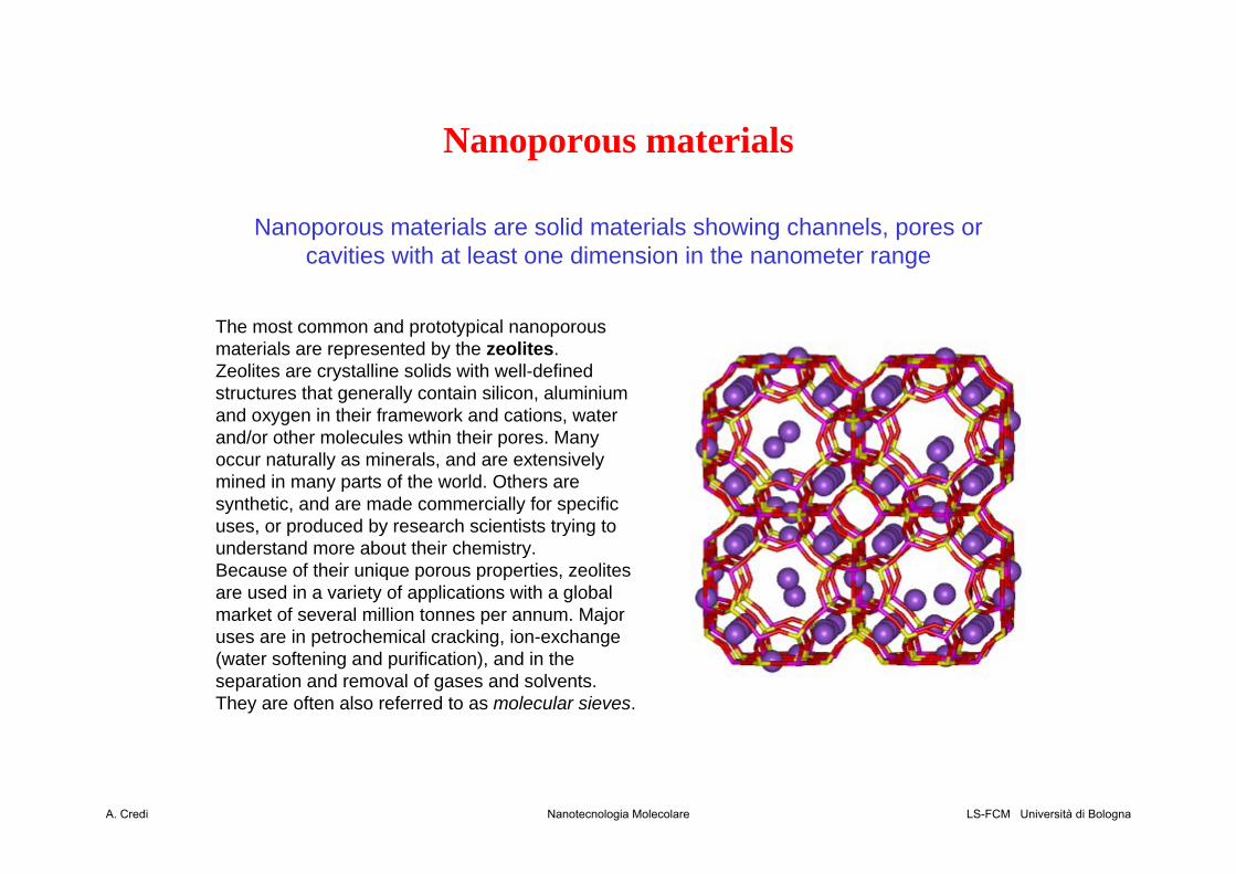
Nanoporous materials
The most common and prototypical nanoporousmaterials are represented by the zeolites.Zeolites are crystalline solids with well-definedstructures that generally contain silicon, aluminiumand oxygen in their framework and cations, water and/or other molecules wthin their pores. Manyoccur naturally as minerals, and are extensivelymined in many parts of the world. Others are synthetic, and are made commercially for specificuses, or produced by research scientists trying tounderstand more about their chemistry.Because of their unique porous properties, zeolitesare used in a variety of applications with a globalmarket of several million tonnes per annum. Major uses are in petrochemical cracking, ion-exchange(water softening and purification), and in the separation and removal of gases and solvents. They are often also referred to as molecular sieves.
Nanoporous materials are solid materials showing channels, pores or cavities with at least one dimension in the nanometer range
A. Credi Nanotecnologia Molecolare LS-FCM Università di Bologna

The framework structure of zeolites
A defining feature of zeolites is that their frameworks are made up of 4-connected networks of atoms. One way of thinking about this is in terms of tetrahedra, with a silicon atom in the middle and oxygen atoms at the corners. These tetrahedra can then link together by their corners (seeillustration below) to from a rich variety of beautiful structures. The framework structure may containlinked cages, cavities or channels, which are of the right size to allow small molecules to enter - i.e. the limiting pore sizes are roughly between 3 and 10 Å in diameter.
In all, over 130 different framework structures are now known. In addition to having silicon or aluminium as the tetrahedral atom, other compositions have also been synthesised, including the growing category of microporous aluminophosphates, known as ALPOs.
A. Credi Nanotecnologia Molecolare LS-FCM Università di Bologna

Applications of zeolitesCatalysisZeolites have the ability to act as catalysts for chemical reactions which take place within the internal cavities. Animportant class of reactions is that catalysed by hydrogen-exchanged zeolites, whose framework-bound protons giverise to very high acidity. This is exploited in many organic reactions, including crude oil cracking, isomerisation and fuelsynthesis. Zeolites can also serve as oxidation or reduction catalysts, often after metals have been introduced into the framework. Examples are the use of titanium ZSM-5 in the production of caprolactam, and copper zeolites in NOxdecomposition.Underpinning all these types of reaction is the unique microporous nature of zeolites, where the shape and size of a particular pore system exerts a steric influence on the reaction, controlling the access of reactants and products. Thuszeolites are often said to act as shape-selective catalysts. Increasingly, attention has focused on fine-tuning the properties of zeolite catalysts in order to carry out very specific syntheses of high-value chemicals e.g. pharmaceuticalsand cosmetics.
Adsorption and SeparationThe shape-selective properties of zeolites are also the basis for their use in molecular adsorption. The ability preferentially to adsorb certain molecules, while excluding others, has opened up a wide range of molecular sieving applications. Sometimes it is simply a matter of the size and shape of pores controlling access into the zeolite. In other cases different types of molecule enter the zeolite, but some diffuse through the channels more quickly, leaving others stuck behind, as in the purification of para-xylene by silicalite. Cation-containing zeolites are extensively used as desiccants due to their high affinity for water, and also find application in gas separation, where molecules are differentiated on the basis of their electrostatic interactions with the metal ions. Conversely, hydrophobic silica zeolites preferentially absorb organic solvents. Zeolites can thus separate molecules based on differences of size, shape and polarity.
Ion ExchangeThe loosely-bound nature of extra-framework metal ions (such as in zeolite NaA) means that they are often readily exchanged for other types of metal when in aqueous solution. This is exploited in a major way in water softening, where alkali metals such as sodium or potassium prefer to exchange out of the zeolite, being replaced by the "hard" calcium and magnesium ions from the water. Many commercial washing powders thus contain substantial amounts of zeolite. Commercial waste water containing heavy metals, and nuclear effluents containing radioactive isotopes can also be cleaned up using such zeolites.
A. Credi Nanotecnologia Molecolare LS-FCM Università di Bologna

Guests entrapment in zeolites
Zeolites can be easily “loaded” with molecular guests that can enter the pores. Interesting types of guests in this regard are catalysts and dyes.
Guests that are larger than the pores can also be incorporated Inside the cavities of zeolites (ship-in-a-bottle complexes). Most often, the entrapped guests are catalytically active metal compounds.
Ship-in-a-bottle complexes can be prepared in two different ways:• (i) synthesis of the guest (e.g., assembly of the metal complex) within the cavity by externally adding the reactants (i.e. metal ions and ligands)• (ii) synthesis of the zeolite around the preformed guest, also referred to as the build-bottle-around-ship approach.
A. Credi Nanotecnologia Molecolare LS-FCM Università di Bologna
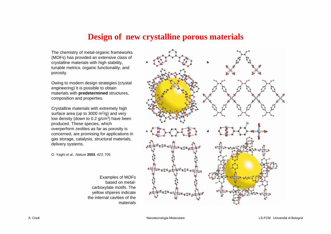
Design of new crystalline porous materials
The chemistry of metal-organic frameworks (MOFs) has provided an extensive class of crystalline materials with high stability, tunable metrics, organic functionality, and porosity.
Owing to modern design strategies (crystal engineering) it is possible to obtain materials with predetermined structures, composition and properties.
Crystalline materials with extremely high surface area (up to 3000 m2/g) and very low density (down to 0.2 g/cm3) have been produced. These species, which overperform zeolites as far as porosity is concerned, are promising for applications in gas storage, catalysis, structural materials, delivery systems.
O. Yaghi et al., Nature 2003, 423, 705
Examples of MOFs based on metal-
carboxylate motifs. The yellow shperes indicate
the internal cavities of the materials
A. Credi Nanotecnologia Molecolare LS-FCM Università di Bologna


