PRELIMINARY DATA SHEET SKY5 -8255-11 Front-End Module for ... › - › media › SkyWorks ›...
39
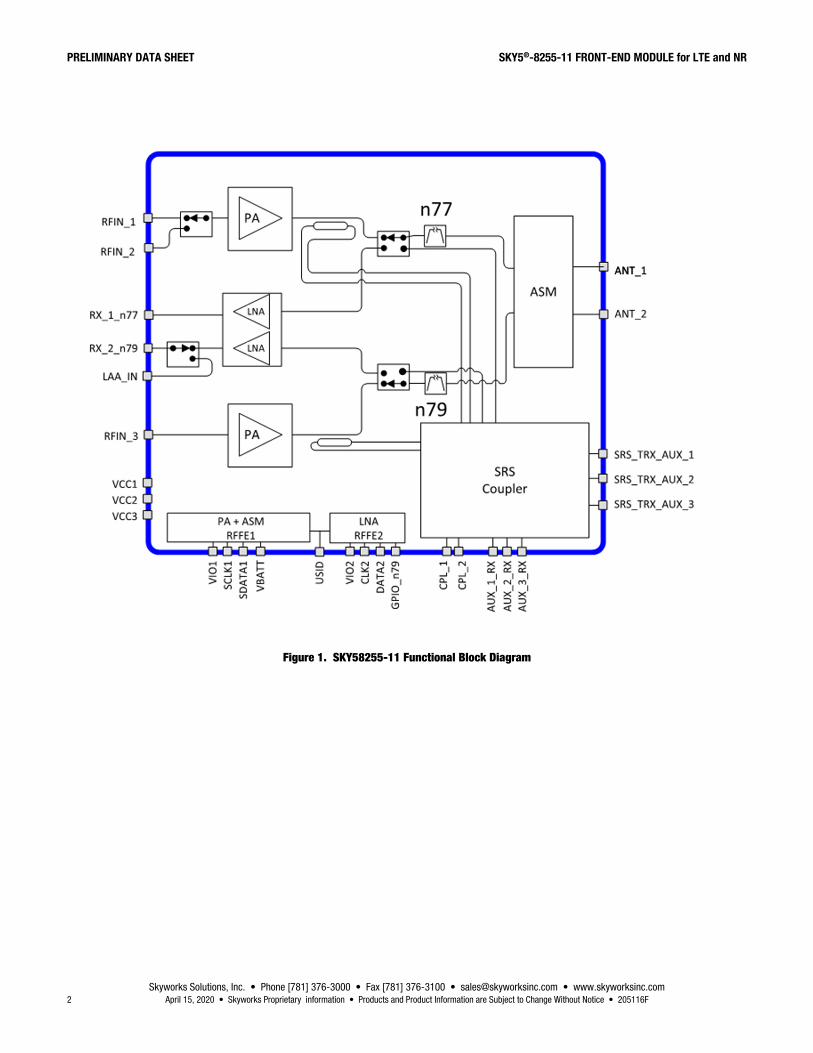
Skyworks Solutions, Inc. • Phone [781] 376-3000 • Fax [781] 376-3100 • [email protected] • www.skyworksinc.com 205116F • Skyworks Proprietary information • Products and Product Information are Subject to Change Without Notice • April 15, 2020 1 PRELIMINARY DATA SHEET SKY5 ® -8255-11 Front-End Module for LTE and NR Bands Applications • Multi-band 4G/5G handsets - Band B42, B43, B48, n77, n78, and n79 - Support n77, n79 Downlink CA Features • Fully Baseband Agnostic Design • Full Power APT support without DPD • UHB S-PAD covering B42, B43, B48, n77, n78, n79, and separate Auxiliary TX • MIPI ® v2.1 compliant 52 MHz RFFE bus • Two ET/APT PA cores • Two LNA cores • Support 2x2 UL-MIMO using two TX placements • Support Fast SRS Hopping timing requirements • Supports system connectivity for: - MIMO-UL with single-feed or diplexed/separate-feed n77/n79 - SISO-UL with single-feed or diplexed/separate-feed n77/n79 • ASM switch with two selectable ANT ports and 6 AUX ports for seamless SRS Hopping support • Switchable LAA input • 50 ohm input/output impedance with internal DC-blocking • Continuous bias control via RFFE interface • Low Supply voltage • Low leakage current in power-down mode Features • Supports full SRS connectivity with minimal external switches • SRS RX ports for sharing coax cables • Integrated Antenna and band select switches • Integrated LNA with MIPI ® control features - up to seven gain modes - independent gain and bias control • Integrated wide bandwidth filters • Small, low profile package - 4.5 mm x 5.5 mm x 0.7 mm (Max.) - 42-pad configuration (includes 20-pad ground array) Description SKY58255-11 is a recent addition to our Sky5 portfolio of 5G Technology products. This versatile and fully matched Front-End Module (FEM) supports multi-band 4G/5G and LTE/NR applications. Packaged in a single 4.5 mm x 5.5 mm x 0.7 mm (Max.) form factor, the 42-pad surface mount (SMT) module consists of PA blocks, input and output matching, a MIPI standard digital control block, single-ended filters, antenna and band- select switches and low Noise amplifier (LNA). Utilizing an enhanced architecture, SKY58255-11 covers multiple bands and meets the spectral linearity requirements of CP-OFDM and DFTS-OFDM modulations with up to 100 MHz bandwidth and up to 273 resource block allocations. Output power is controlled by varying input power and adjusting VCC maximizes efficiency. Extremely low leakage current maximizes handset stand-by time.
Transcript of PRELIMINARY DATA SHEET SKY5 -8255-11 Front-End Module for ... › - › media › SkyWorks ›...

Skyworks Solutions, Inc. • Phone [781] 376-3000 • Fax [781] 376-3100 • [email protected] • www.skyworksinc.com 205116F • Skyworks Proprietary information • Products and Product Information are Subject to Change Without Notice • April 15, 2020 1
PRELIMINARY DATA SHEET
SKY5®-8255-11 Front-End Module for LTE and NR Bands Applications • Multi-band 4G/5G handsets
- Band B42, B43, B48, n77, n78, and n79 - Support n77, n79 Downlink CA
Features • Fully Baseband Agnostic Design
• Full Power APT support without DPD
• UHB S-PAD covering B42, B43, B48, n77, n78, n79, and separate Auxiliary TX
• MIPI® v2.1 compliant 52 MHz RFFE bus
• Two ET/APT PA cores
• Two LNA cores
• Support 2x2 UL-MIMO using two TX placements
• Support Fast SRS Hopping timing requirements
• Supports system connectivity for: - MIMO-UL with single-feed or diplexed/separate-feed n77/n79 - SISO-UL with single-feed or diplexed/separate-feed n77/n79
• ASM switch with two selectable ANT ports and 6 AUX ports for seamless SRS Hopping support
• Switchable LAA input
• 50 ohm input/output impedance with internal DC-blocking
• Continuous bias control via RFFE interface
• Low Supply voltage
• Low leakage current in power-down mode
Features • Supports full SRS connectivity with minimal external switches
• SRS RX ports for sharing coax cables
• Integrated Antenna and band select switches
• Integrated LNA with MIPI® control features - up to seven gain modes - independent gain and bias control
• Integrated wide bandwidth filters
• Small, low profile package - 4.5 mm x 5.5 mm x 0.7 mm (Max.) - 42-pad configuration (includes 20-pad ground array)
Description SKY58255-11 is a recent addition to our Sky5 portfolio of 5G Technology products. This versatile and fully matched Front-End Module (FEM) supports multi-band 4G/5G and LTE/NR applications. Packaged in a single 4.5 mm x 5.5 mm x 0.7 mm (Max.) form factor, the 42-pad surface mount (SMT) module consists of PA blocks, input and output matching, a MIPI standard digital control block, single-ended filters, antenna and band-select switches and low Noise amplifier (LNA).
Utilizing an enhanced architecture, SKY58255-11 covers multiple bands and meets the spectral linearity requirements of CP-OFDM and DFTS-OFDM modulations with up to 100 MHz bandwidth and up to 273 resource block allocations. Output power is controlled by varying input power and adjusting VCC maximizes efficiency. Extremely low leakage current maximizes handset stand-by time.
PRELIMINARY DATA SHEET SKY5®-8255-11 FRONT-END MODULE for LTE and NR
Skyworks Solutions, Inc. • Phone [781] 376-3000 • Fax [781] 376-3100 • [email protected] • www.skyworksinc.com 2 April 15, 2020 • Skyworks Proprietary information • Products and Product Information are Subject to Change Without Notice • 205116F
Figure 1. SKY58255-11 Functional Block Diagram

SKY5®-8255-11 FRONT-END MODULE for LTE and NR PRELIMINARY DATA SHEET
Skyworks Solutions, Inc. • Phone [781] 376-3000 • Fax [781] 376-3100 • [email protected] • www.skyworksinc.com 205116F • Skyworks Proprietary information • Products and Product Information are Subject to Change Without Notice • April 15, 2020 3
Table 1. SKY58255-11 Supported Bands and Modes
Band Modes Supported LTE Bandwidths (MHz) ET / APT
42 TDD LTE 5, 10, 15, 20 ET /APT
43 TDD LTE 5, 10, 15, 20 ET /APT
48 TDD LTE 5, 10, 15, 20 ET /APT
n77 TDD NR 5, 10, 5, 20, 25, 30, 40, 50, 60, 80, 100 ET /APT
n78 TDD NR 5, 10, 5, 20, 25, 30, 40, 50, 60, 80, 100 ET /APT
n79 TDD NR 40, 50, 60, 80, 100 ET /APT
Table 2. SKY58255-11 Absolute Maximum Operating Conditions
Parameter Symbol Condition Min Typ Max Unit
RF input power PIN 152 dBm
Supply Voltage4 VBATT No RF –0.53 3.8 6.0 V
RF –0.53 3.8 5.5
VDD –0.53 1.2 2.2
VCC1, VCC2, VCC3 –0.53 6.0
Digital Control Lines SCLK1,SDATA1, VIO1 –0.5 2.2 V
CLK2, DATA2, VIO2
Case Temperatures TCASE Operating –30 +110 °C
TSTG Storage –30 +150
Electrostatic Discharge Sensitivity IEC IEC 61000-4-2 TBD V
ESD_HBM Human Body Model RX Pad (Class 1C) –1000 1000
Human Body Model RF Pads (Class 1B) –1000 1000
Human Body Model Other (Class 1A) –1000 1000
ESD_CDM Charged Device Model (Class C2) –500 500
Leakage Current Power-down Mode, VBATT = 5.5 V 0 30 50 μA
1 Exposure to maximum rating conditions for extended periods may reduce device reliability. No damage to device with only one parameter set at the limit and all other parameters set at or below their nominal value.
2 50 Ω load applied CW 3 Pulsed at –1.2 V for 100 μs 4 2.5 day cumulative over 10 years
Table 3. SKY58255-11 Recommended Operating Conditions
Parameter Condition Min. Typ. Max. Unit
Supply Voltage VBATT 3.0 5.5 V
VDD 1.15 1.21 1.95
VCC1, VCC2, VCC3 0.5 5.5
Digital Control Signals Low 0 0.5 V
High 1.35 1.8 2.0
Current 50 μA
On/Off Time DC: ICC to within 90% of final value 5 μs
RF: POUT within 1dB of final value 2
Ambient Temperature 3GPP –20 +25 +85 °C

PRELIMINARY DATA SHEET SKY5®-8255-11 FRONT-END MODULE for LTE and NR
Skyworks Solutions, Inc. • Phone [781] 376-3000 • Fax [781] 376-3100 • [email protected] • www.skyworksinc.com 4 April 15, 2020 • Skyworks Proprietary information • Products and Product Information are Subject to Change Without Notice • 205116F
Table 4-1. SKY58255-11 – n77_n78_B42_B43_B48_TX_ANT
Band Parameter Symbol Conditions Min. Typ. Max. Unit
n77 Frequency Range ƒ_RANGE 3300 4200 MHz
n78 Frequency Range ƒ_RANGE 3300 3800 MHz
B42 Frequency Range ƒ_RANGE 3400 3600 MHz
B43 Frequency Range ƒ_RANGE 3600 3800 MHz
B48 Frequency Range ƒ_RANGE 3550 3700 MHz
n77, n78, B42, B43, B48
Vcc Voltage Range V_RANGE 0.5 5.5 V
n77 NR Operating Power Range P_RANGE –40 26 – MPR dBm
n78 NR Operating Power Range P_RANGE –40 28.5 – MPR dBm
B42, B43, B48 LTE Operating Power Range P_RANGE –40 29 – MPR dBm
n78 NR Max RMS Output Power PC2, ET PRATED NTC up to 3.8 GHz 28.5 dBm
n78 NR Max RMS Output Power PC2, ET PRATED ETC up to 3.8 GHz 27.5 dBm
n78 NR Max RMS Output Power PC2, APT ULPM PRATED NTC –9 dBm
n78 NR Max RMS Output Power PC2, APT ULPM PRATED ETC –9 dBm
n78 NR Max RMS Output Power PC2, APT HPM PRATED NTC 28.5 dBm
n78 NR Max RMS Output Power PC2, APT HPM PRATED ETC 27.5 dBm
n77 NR Max RMS Output Power PC3, ET PRATED NTC 26 dBm
n77 NR Max RMS Output Power PC3, ET PRATED ETC 25 dBm
n77 NR Max RMS Output Power PC3, APT ULPM PRATED NTC –9 dBm
n77 NR Max RMS Output Power PC3, APT ULPM PRATED ETC –9 dBm
n77 NR Max RMS Output Power PC3, APT HPM PRATED NTC 26 dBm
n77 NR Max RMS Output Power PC3, APT HPM PRATED ETC 25 dBm
B42, B43, B48 LTE Max RMS Output Power, ET PRATED NTC 29 dBm
B42, B43, B48 LTE Max RMS Output Power, ET PRATED ETC 28 dBm
B42, B43, B48 LTE Max RMS Output Power, APT ULPM PRATED NTC –9 dBm
B42, B43, B48 LTE Max RMS Output Power, APT ULPM PRATED ETC –9 dBm
n78, B42, B43, B48 NR Max ET Power Gain G_NR NTC 30 dB
n78, B42, B43, B48 NR Max ET Power Gain G_NR ETC 28 dB
n78, B42, B43, B48 NR Max APT HPM Power Gain G_NR NTC 30.2 33.0 dB
n78, B42, B43, B48 NR Max APT HPM Power Gain G_NR ETC 27.7 33.9 dB
n78, B42, B43, B48 NR Max APT ULPM Power Gain G_NR NTC 9.3 12.3 14.1 dB
n78, B42, B43, B48 NR Max APT ULPM Power Gain G_NR ETC 6.5 12.3 15.7 dB
n78, B42, B43, B48 Gain Ripple ETC 0.5 dB
n77 NR Max ET Power Gain G_NR NTC 30 dB
n77 NR Max ET Power Gain G_NR ETC 28 dB
n77 NR Max APT HPM Power Gain G_NR NTC 27.0 32.3 dB
n77 NR Max APT HPM Power Gain G_NR ETC 24.9 33.5 dB
n77 NR Max APT ULPM Power Gain G_NR NTC 9.3 12.3 14.1 dB
n77 NR Max APT ULPM Power Gain G_NR ETC 6.5 12.3 15.7 dB
n77 Gain Ripple ETC 0.5 dB
n78 Gain at 2nd Harmonic G_2ƒo ETC –12.3 –10.1 –7.7 dB
n78 Gain at 3rd Harmonic G_3ƒo ETC –29.8 –27.9 –26.3 dB

SKY5®-8255-11 FRONT-END MODULE for LTE and NR PRELIMINARY DATA SHEET
Skyworks Solutions, Inc. • Phone [781] 376-3000 • Fax [781] 376-3100 • [email protected] • www.skyworksinc.com 205116F • Skyworks Proprietary information • Products and Product Information are Subject to Change Without Notice • April 15, 2020 5
Table 4-2. SKY58255-11 – n77_n78_B42_B43_B48_TX_ANT
Band Parameter Symbol Conditions Min. Typ. Max. Unit
n78 Gain at 4th Harmonic G_4ƒo ETC dB
n78 Gain at 5th Harmonic G_5ƒo ETC dB
n78 Gain in GNSS L5(1164 - 1189 MHz) G_L5 ETC –39.4 –37.3 –34.7 dB
n78 Gain in GPS/GLONASS G_GPS ETC –20.4 –18.2 –16.4 dB
n78 Gain in 2.4 GHz Wifi G_ISM ETC 5.2 7.8 9.8 dB
n78 Gain in 5 GHz Wifi G_WIFI ETC 13.3 15.7 17.8 dB
n77 Gain at 2nd Harmonic G_2ƒo ETC –12.5 –10.6 –9.1 dB
n77 Gain at 3rd Harmonic G_3ƒo ETC –29.0 –27.1 –25.4 dB
n77 Gain at 4th Harmonic G_4ƒo ETC dB
n77 Gain at 5th Harmonic G_5ƒo ETC dB
n77 Gain in GNSS L5(1164 - 1189 MHz) G_L5 ETC –38.0 –36.9 –33.3 dB
n77 Gain in GPS/GLONASS G_GPS ETC –21.0 –19.2 –17.7 dB
n77 Gain in 2.4 GHz Wifi G_ISM ETC 4.6 6.8 8.7 dB
n77 Gain in 5 GHz Wifi G_WIFI ETC 13.3 15.4 17.2 dB
n77 NR, ET Max Power Current SYS_IBATT1 NTC, Max Power, MPR=0, PC3 (3.8-4.2GHz region only), 60MHz BW
mA
n78 NR, ET Max Power Current SYS_IBATT1 NTC, Max Power, MPR=0, PC2, 60MHz BW
mA
B42, B43, B48 LTE, ET Max Power Current SYS_IBATT1 NTC, Max Power, MPR=0, PC2, 60MHz BW
mA
n78 NR APT HPM Current Consumption ICC2 NTC, 100 MHz BW; PC2 824.9 859.5 887.6 mA
n77 NR APT HPM Current Consumption ICC2 NTC, 100 MHz BW; PC2 634.0 680.1 752.6 mA
B42, B43, B48 LTE EVM, ET EVM NTC 1.85 %
B42, B43, B48 LTE EVM, APT LPM EVM NTC 1.85 %
B42, B43, B48 LTE E-UTRA ACLR, ET E_UTRA ACLR
NTC –36 dBc
B42, B43, B48 LTE E-UTRA ACLR, APT LPM E_UTRA ACLR
NTC –58.8 –56.4 –53.2 dBc
B42, B43, B48 LTE UTRA1 ACLR, ET UTRA1 ACLR
NTC –38 dBc
B42, B43, B48 LTE UTRA1 ACLR, APT LPM UTRA1 ACLR
NTC –38 dBc
B42, B43, B48 LTE UTRA2 ACLR, ET UTRA2 ACLR
NTC –38 dBc
B42, B43, B48 LTE UTRA2 ACLR, APT LPM UTRA2 ACLR
NTC –38 dBc
n78 NR EVM with Outer RB, ET EVM NTC 1.85 %
n78 NR EVM with Outer RB, APT HPM/LPM3 EVM NTC 1.7 1.8 2.0 %
n78 NR-ACLR with Outer RB, ET NR ACLR NTC –36 dBc
n78 NR-ACLR with Outer RB, APT HPM/LPM4 NR ACLR NTC –35.4 –33.3 dBc
n78 NR-ACLR with Inner RB, ET NR ACLR NTC –36 dBc
n78 NR-ACLR with Inner RB, APT HPM/LPM5 NR ACLR NTC –38.9 –38.4 dBc
n78 NR-ACLR with Edge RB, ET NR ACLR NTC –36 dBc
n78 NR-ACLR with Edge RB, APT HPM/LPM NR ACLR NTC –36 dBc
n77 NR EVM with Outer RB, ET EVM NTC 1.6 1.7 %
n77 NR EVM with Outer RB, APT HPM/LPM3 EVM NTC 1.85 %

PRELIMINARY DATA SHEET SKY5®-8255-11 FRONT-END MODULE for LTE and NR
Skyworks Solutions, Inc. • Phone [781] 376-3000 • Fax [781] 376-3100 • [email protected] • www.skyworksinc.com 6 April 15, 2020 • Skyworks Proprietary information • Products and Product Information are Subject to Change Without Notice • 205116F
Table 4-3. SKY58255-11 – n77_n78_B42_B43_B48_TX_ANT
Band Parameter Symbol Conditions Min. Typ. Max. Unit
n77 NR-ACLR with Outer RB, ET NR ACLR NTC –36 dBc
n77 NR-ACLR with Outer RB, APT HPM/LPM4 NR ACLR NTC –37.7 –33.0 dBc
n77 NR-ACLR with Inner RB, ET NR ACLR NTC -36 dBc
n77 NR-ACLR with Inner RB, APT HPM/LPM5 NR ACLR NTC –37.0 –36.4 dBc
n77 NR-ACLR with Edge RB, ET NR ACLR NTC -36 dBc
n77 NR-ACLR with Edge RB, APT HPM/LPM NR ACLR NTC -36 dBc
B42, B43, B48 2nd Harmonic P2ƒo NTC -35 dBm
B42, B43, B48 3rd Harmonic P3ƒo NTC -35 dBm
n77 2nd Harmonic P2ƒo NTC –48.2 –40.0 dBm
n77 3rd Harmonic P3ƒo NTC –56.7 –49.0 dBm
n77 4th Harmonic P4ƒo NTC –50.0 dBm
n77 5th Harmonic P5ƒo NTC –60.0 dBm
n77 2.4 GHz WiFi Band Noise n_ISM NTC –160.7 –155.5 dBm/Hz
n77 5 GHz WiFi Band Noise n_WIFI NTC –160.2 –149.1 dBm/Hz
n77 GPS, GLONASS, Beidu Band Noise n_GPS NTC –177.4 –168.6 dBm/Hz
n77 GPS L5 Band Noise n_L5 NTC –179.5 –168.7 dBm/Hz
n77 Rx-B1 Emissions n_OOB NTC –176.1 –166.7 dBm/Hz
n77 Rx-B3 Emissions n_OOB NTC –177.2 –167.5 dBm/Hz
n77 Rx-B5 Emissions n_OOB NTC –180.3 –170.2 dBm/Hz
n77 Rx-B7 Emissions n_OOB NTC –169.4 –162.9 dBm/Hz
n77 Rx-B8 Emissions n_OOB NTC –179.8 –170.1 dBm/Hz
n77 Rx-B11 Emissions n_OOB NTC –178.0 –169.3 dBm/Hz
n77 Rx-B18 Emissions n_OOB NTC –179.8 –168.8 dBm/Hz
n77 Rx-B19 Emissions n_OOB NTC –179.4 –171.1 dBm/Hz
n77 Rx-B20 Emissions n_OOB NTC –179.8 –170.4 dBm/Hz
n77 Rx-B21 Emissions n_OOB NTC –177.7 –168.6 dBm/Hz
n77 Rx-B26 Emissions n_OOB NTC –180.3 –170.7 dBm/Hz
n77 Rx-B28 Emissions n_OOB NTC –179.8 –169.9 dBm/Hz
n77 Rx-B34 Emissions n_OOB NTC –176.3 –167.1 dBm/Hz
n77 Rx-B38 Emissions n_OOB NTC –166.2 –160 dBm/Hz
n77 Rx-B39 Emissions n_OOB NTC –175.9 –167 dBm/Hz
n77 Rx-B40 Emissions n_OOB NTC –167.1 –158.4 dBm/Hz
n77 Rx-B41 Emissions n_OOB NTC –165.7 –156.8 dBm/Hz
n78 2nd Harmonic P2ƒo NTC –47.9 –41 dBm
n78 3rd Harmonic P3ƒo NTC –51.3 –44.8 dBm
n78 4th Harmonic P4ƒo NTC –40.0 dBm
n78 5th Harmonic P5ƒo NTC –50.0 dBm
n78 2.4 GHz WiFi Band Noise n_ISM NTC –158.2 –151.7 dBm/Hz
n78 5 GHz WiFi Band Noise n_WIFI NTC –159.4 –150.7 dBm/Hz
n78 GPS, GLONASS, Beidu Band Noise n_GPS NTC –175.9 –167.8 dBm/Hz
n78 GPS L5 Band Noise n_L5 NTC –179.3 –170.7 dBm/Hz
n78 Rx-B1 Emissions n_OOB NTC –175.4 –165.9 dBm/Hz
n78 Rx-B3 Emissions n_OOB NTC –176.3 –168.7 dBm/Hz
n78 Rx-B5 Emissions n_OOB NTC –179.2 –169.1 dBm/Hz
n78 Rx-B7 Emissions n_OOB NTC –167.7 –160.6 dBm/Hz
n78 Rx-B8 Emissions n_OOB NTC –179.7 –170.0 dBm/Hz

SKY5®-8255-11 FRONT-END MODULE for LTE and NR PRELIMINARY DATA SHEET
Skyworks Solutions, Inc. • Phone [781] 376-3000 • Fax [781] 376-3100 • [email protected] • www.skyworksinc.com 205116F • Skyworks Proprietary information • Products and Product Information are Subject to Change Without Notice • April 15, 2020 7
Table 4-4. SKY58255-11 – n77_n78_B42_B43_B48_TX_ANT
Band Parameter Symbol Conditions Min. Typ. Max. Unit
n78 Rx-B11 Emissions n_OOB NTC –176.9 –169.4 dBm/Hz
n78 Rx-B18 Emissions n_OOB NTC –179.7 –170.0 dBm/Hz
n78 Rx-B19 Emissions n_OOB NTC –179.9 –169.3 dBm/Hz
n78 Rx-B20 Emissions n_OOB NTC –180.1 –170.5 dBm/Hz
n78 Rx-B21 Emissions n_OOB NTC –177.3 –166.8 dBm/Hz
n78 Rx-B26 Emissions n_OOB NTC –179.7 –169.1 dBm/Hz
n78 Rx-B28 Emissions n_OOB NTC –180.2 –170.7 dBm/Hz
n78 Rx-B34 Emissions n_OOB NTC –176.3 –167.5 dBm/Hz
n78 Rx-B38 Emissions n_OOB NTC –163.9 –156.3 dBm/Hz
n78 Rx-B39 Emissions n_OOB NTC –177.1 –167.4 dBm/Hz
n78 Rx-B40 Emissions n_OOB NTC –164.5 –152.9 dBm/Hz
n78 Rx-B41 Emissions n_OOB NTC –163.2 –152.6 dBm/Hz
B42, B43 Rx-B27 Emissions n_OOB NTC –168 dBm/Hz
B42, B43 Rx-B31 Emissions n_OOB NTC –168 dBm/Hz
B42, B43 Rx-B32 Emissions n_OOB NTC –168 dBm/Hz
B42, B43 Rx-B44 Emissions n_OOB NTC –168 dBm/Hz
B42, B43 Rx-B45 Emissions n_OOB NTC –166 dBm/Hz
B42, B43, B48 Rx-B50 Emissions n_OOB NTC –166 dBm/Hz
B42, B43, B48 Rx-B51 Emissions n_OOB NTC –166 dBm/Hz
B42, B43, B48 Rx-B66 Emissions n_OOB NTC – dBm/Hz
B42, B43 Rx-B67 Emissions n_OOB NTC –166 dBm/Hz
B42, B43 Rx-B68 Emissions n_OOB NTC –166 dBm/Hz
B42, B43 Rx-B69 Emissions n_OOB NTC –166 dBm/Hz
B42, B43 Rx-B72 Emissions n_OOB NTC –166 dBm/Hz
B42, B43 Rx-B73 Emissions n_OOB NTC –166 dBm/Hz
B42, B43, B48 Rx-B74 Emissions n_OOB NTC –166 dBm/Hz
B42, B4 Rx-B75 Emissions n_OOB NTC –166 dBm/Hz
B42, B4 Rx-B76 Emissions n_OOB NTC –56 dBm/Hz
B42, B4 NS22 Margin NS22 NTC 3 dB
B42, B4 NS23 Margin NS23 NTC 3 dB
B48 NS27 Margin NS27 NTC 3 dB
Notes
1 Assuming 75% ET tracker efficiency 2 VCC = 5.5 V 3 Outer full TDi_CP_256_100 MHz_273RB_0_30 MPR 6.5 4 Outer full TD!_CP_4_100 MHz_273 RB_0_30 MPR 3 5 Inner ful TDI_DFT_4_100 MHz_135RB_71_30 MPR 0
PRELIMINARY DATA SHEET SKY5®-8255-11 FRONT-END MODULE for LTE and NR
Skyworks Solutions, Inc. • Phone [781] 376-3000 • Fax [781] 376-3100 • [email protected] • www.skyworksinc.com 8 April 15, 2020 • Skyworks Proprietary information • Products and Product Information are Subject to Change Without Notice • 205116F
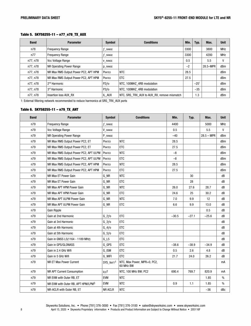
Table 5. SKY58255-11 – n77_n78_TX_AUX
Band Parameter Symbol Conditions Min. Typ. Max. Unit
n78 Frequency Range ƒ_RANGE 3300 3800 MHz
n77 Frequency Range ƒ_RANGE 3300 4200 MHz
n77, n78 Vcc Voltage Range v_RANGE 0.5 5.5 V
n77, n78 NR Operating Power Range p_RANGE –2 28.5–MPR dBm
n77, n78 NR Max RMS Output Power PC2, APT HPM PRATED NTC 28.5 dBm
n77, n78 NR Max RMS Output Power PC2, APT HPM PRATED ETC 27.5 dBm
n77, n78 2nd Harmonic P2ƒo NTC, 100MHZ_4RB modulation –251 dBm
n77, n78 3rd Harmonic P3ƒo NTC, 100MHZ_4RB modulation –35 dBm
n77, n78 Insertion loss AUX_RX IL_AUX NTC, SRS_TRX_AUX to AUX_RX, remove mismatch 1.3 dBm
1: External filtering network recommended to reduce harmonics at SRS_TRX_AUX ports
Table 6. SKY58255-11 – n79_TX_ANT
Band Parameter Symbol Conditions Min. Typ. Max. Unit
n79 Frequency Range ƒ_RANGE 4400 5000 MHz
n79 Vcc Voltage Range V_RANGE 0.5 5.5 V
n79 NR Operating Power Range P_RANGE –40 28.5 – MPR dBm
n79 NR Max RMS Output Power PC2, ET PRATED NTC 28.5 dBm
n79 NR Max RMS Output Power PC2, ET PRATED ETC 27.5 dBm
n79 NR Max RMS Output Power PC2, APT ULPM PRATED NTC –8 dBm
n79 NR Max RMS Output Power PC2, APT ULPM PRATED ETC –8 dBm
n79 NR Max RMS Output Power PC2, APT HPM PRATED NTC 28.5 dBm
n79 NR Max RMS Output Power PC2, APT HPM PRATED ETC 27.5 dBm
n79 NR Max ET Power Gain G_NR NTC 30 dB
n79 NR Max ET Power Gain G_NR ETC 28 dB
n79 NR Max APT HPM Power Gain G_NR NTC 26.0 27.6 28.7 dB
n79 NR Max APT HPM Power Gain G_NR ETC 24.6 25 30.2 dB
n79 NR Max APT ULPM Power Gain G_NR NTC 7.0 9.9 12 dB
n79 NR Max APT ULPM Power Gain G_NR ETC 6.6 9.9 13.0 dB
n79 Gain Ripple 0.5 dB
n79 Gain at 2nd Harmonic G_2ƒo ETC –30.5 –27.1 –25.6 dB
n79 Gain at 3rd Harmonic G_3ƒo ETC dB
n79 Gain at 4th Harmonic G_4ƒo ETC dB
n79 Gain at 5th Harmonic G_5ƒo ETC dB
n79 Gain in GNSS L5(1164 - 1189 MHz) G_L5 ETC dB
n79 Gain in GPS/GLONASS G_GPS ETC –38.6 –38.9 –34.9 dB
n79 Gain in 2.4 GHz Wifi G_ISM ETC 0.5 2.6 4.8 dB
n79 Gain in 5 GHz Wifi G_WIFI ETC 21.7 24.0 26.2 dB
n79 NR ET Max Power Current SYS_IBATT1 NTC, Max Power, MPR=0, PC2, 60 MHz BW
mA
n79 NR APT Current Consumption ICC2 NTC, 100 MHz BW; PC2 690.4 769.7 820.9 mA
n79 NR EVM with Outer RB, ET EVM NTC 1.85 %
n79 NR EVM with Outer RB, APT HPM/LPM3 EVM NTC 0.9 1.1 1.85 %
n79 NR-ACLR with Outer RB, ET NR ACLR NTC –36 dBc

SKY5®-8255-11 FRONT-END MODULE for LTE and NR PRELIMINARY DATA SHEET
Skyworks Solutions, Inc. • Phone [781] 376-3000 • Fax [781] 376-3100 • [email protected] • www.skyworksinc.com 205116F • Skyworks Proprietary information • Products and Product Information are Subject to Change Without Notice • April 15, 2020 9
Notes
1 Assuming 75% ET tracker efficiency 2 VCC = 5.5 V 3 Outer full TDi_CP_256_100 MHz_273RB_0_30 MPR 6.5
Table 7. SKY58255-11 – n79_TX_ANT
Band Parameter Symbol Conditions Min. Typ. Max. Unit
n79 NR-ACLR with Outer RB, APT HPM/LPM1 NR ACLR NTC –37.1 –35.2 dBc
n79 NR-ACLR with Inner RB, ET NR ACLR NTC –36 dBc
n79 NR-ACLR with Inner RB, APT HPM/LPM2 NR ACLR NTC –38.1 –37.6 dBc
n79 NR-ACLR with Edge RB, ET NR ACLR NTC –36 dBc
n79 NR-ACLR with Edge RB, APT HPM/LPM NR ACLR NTC –36 dBc
n79 2nd Harmonic P2ƒo NTC –48.9 –40.3 dBm
n79 3rd Harmonic P3ƒo NTC –54.5 –50.8 dBm
n79 4th Harmonic P4ƒo NTC –40.0 dBm
n79 5th Harmonic P5ƒo NTC –50.0 dBm
n79 2.4 GHz WiFi Band Noise n_ISM NTC –166.0 –163.4 dBm/Hz
n79 5 GHz WiFi Band Noise n_WIFI NTC –151.7 –121.4 dBm/Hz
n79 GPS, GLONASS, Beidou Band Noise n_GPS NTC –177.8 –167.8 dBm/Hz
n79 GPS L5 Band Noise n_L5 NTC –178.3 –169.0 dBm/Hz
n79 Rx-B1 Emissions n_OOB NTC –181.9 –176.1 dBm/Hz
n79 Rx-B3 Emissions n_OOB NTC –183.1 –176.3 dBm/Hz
n79 Rx-B5 Emissions n_OOB NTC –186.8 –179.5 dBm/Hz
n79 Rx-B8 Emissions n_OOB NTC –186.1 –179.9 dBm/Hz
n79 Rx-B11 Emissions n_OOB NTC –184.9 –178.1 dBm/Hz
n79 Rx-B18 Emissions n_OOB NTC –186.5 –179.1 dBm/Hz
n79 Rx-B19 Emissions n_OOB NTC –186.3 –178.4 dBm/Hz
n79 Rx-B21 Emissions n_OOB NTC –184.9 –177.2 dBm/Hz
n79 Rx-B28 Emissions n_OOB NTC –187.2 –180.2 dBm/Hz
n79 Rx-B34 Emissions n_OOB NTC –186.5 –176.7 dBm/Hz
n79 Rx-B39 Emissions n_OOB NTC –183.7 –178.7 dBm/Hz
n79 Rx-B40 Emissions n_OOB NTC –171.0 –168.9 dBm/Hz
n79 Rx-B41 Emissions n_OOB NTC –169.4 –162.7 dBm/Hz
Notes
1 Outer full TDI_CP_4_100 MHz_273 RB_0_30 MPR 3 2 Inner ful TDI_DFT_4_100 MHz_135RB_71_30 MPR 1
Table 8. SKY58255-11 – n79_TX_AUX
Band Parameter Symbol Conditions Min. Typ. Max. Unit
n79 Frequency Range ƒ_RANGE 4400 5000 MHz
n79 Vcc Voltage Range V_RANGE 0.5 5.5 V
n79 NR Max RMS Output Power PC2, APT HPM PRATED NTC 28.5 dBm
n79 NR Max RMS Output Power PC2, APT HPM PRATED ETC 27.5 dBm
n79 2nd Harmonic P2ƒo NTC, 100MHZ_4RB modulation –40 dBm
n79 3rd Harmonic P3ƒo NTC, 100MHZ_4RB modulation –45 dBm
n79 Insertion loss AUX_RX IL_AUX NTC, SRS_TRX_AUX to AUX_RX, remove mismatch 1.3 dBm

PRELIMINARY DATA SHEET SKY5®-8255-11 FRONT-END MODULE for LTE and NR
Skyworks Solutions, Inc. • Phone [781] 376-3000 • Fax [781] 376-3100 • [email protected] • www.skyworksinc.com 10 April 15, 2020 • Skyworks Proprietary information • Products and Product Information are Subject to Change Without Notice • 205116F
Table 9. SKY58255-11– Coupler Specification
Band Parameter Symbol Conditions Min. Typ. Max. Unit
Frequency Range f_RANGE 3300 5000 MHz
Coupler Coupling Factor CF_FWD NTC, Forward 24 dB
Coupler Factor CF_RVS NTC, Reverse 24 dB
Coupler Factor Variation CF_Var NTC, Coupler factor variation at VSWR=2.5:1 +/-0.7 dB
CPL SW Insertion loss IL_CPLSW NTC, CPL1 to CPL2 IL, 3.5 4.5 dB
Table 10. SKY58255-11– T8 n77_n78_B42_B43_B48_RX
Band Parameter Symbol Conditions Min. Typ. Max. Unitn77,n78,B42,B43,B48 Frequency Range ƒ_RANGE 3300 4200 MHz
n77,n78,B42,B43,B48 Nominal LNA Current, G7 ILNA NTC 7.4 9.4 mA
n77,n78,B42,B43,B48 Nominal LNA Current, G6 ILNA NTC 6.3 8.1 mA
n77,n78,B42,B43,B48 Nominal LNA Current, G5 ILNA NTC 4.7 6.0 mA
n77,n78,B42,B43,B48 Nominal LNA Current, G4 ILNA NTC 2.5 3.1 mA
n77,n78,B42,B43,B48 Nominal LNA Current, G3 ILNA NTC 1.2 1.5 mA
n77,n78,B42,B43,B48 Nominal LNA Current, G2 ILNA NTC 0.2 0.2 mA
n77,n78,B42,B43,B48 Nominal LNA Current, G1 ILNA NTC 0.2 0.2 mA
n77,n78,B42,B43,B48 In-Band Gain, G7 Gn NTC 15.4 17.6 18.5 dB
n77,n78,B42,B43,B48 In-Band Gain, G6 Gn NTC 14.4 16.5 17.4 dB
n77,n78,B42,B43,B48 In-Band Gain, G5 Gn NTC 8.1 10.8 11.6 dB
n77,n78,B42,B43,B48 In-Band Gain, G4 Gn NTC 1.4 4.0 4.8 dB
n77,n78,B42,B43,B48 In-Band Gain, G3 Gn NTC –5.6 2.5 –1.6 –9.7
n77,n78,B42,B43,B48 In-Band Gain, G2 Gn NTC –9.7 –8.5 –7.8 dB
n77,n78,B42,B43,B48 In-Band Gain, G1 Gn NTC –15.0 –14.0 –13.5 dB
n77,n78,B42,B43,B48 In-BandInput P1dB, G7 P1dB NTC –20.0 dBm
n77,n78,B42,B43,B48 In-BandInput P1dB, G6 P1dB NTC –18.8 dBm
n77,n78,B42,B43,B48 In-BandInput P1dB, G5 P1dB NTC –16.1 dBm
n77,n78,B42,B43,B48 In-BandInput P1dB, G4 P1dB NTC –13.1 dBm
n77,n78,B42,B43,B48 In-BandInput P1dB, G3 P1dB NTC –8.8 dBm
n77,n78,B42,B43,B48 In-BandInput P1dB, G2 P1dB NTC –3.4 dBm
n77,n78,B42,B43,B48 In-BandInput P1dB, G1 P1dB NTC –3.6 dBm
n77,n78,B42,B48 In-Band IIP3, G7 IIP3 NTC, fCW2 = fCW1±1MHz –6.9 dBm
n77,n78,B42,B48 In-Band IIP3, G6 IIP3 NTC, fCW2 = fCW1±1MHz –5.4 dBm
n77,n78,B42,B48 In-Band IIP3, G5 IIP3 NTC, fCW2 = fCW1±1MHz –2.8 dBm
n77,n78,B42,B48 In-Band IIP3, G4 IIP3 NTC, fCW2 = fCW1±1MHz –0.4 dBm
n77,n78,B42,B48 In-Band IIP3, G3 IIP3 NTC, fCW2 = fCW1±1MHz –2.3 dBm
n77,n78,B42,B48 In-Band IIP3, G2 IIP3 NTC, fCW2 = fCW1±1MHz –21.1 dBm
n77,n78,B42,B48 In-Band IIP3, G1 IIP3 NTC, fCW2 = fCW1±1MHz –21.1 dBm
n77,n78,B42,B48 Input Return Loss RL NTC 6.5 dB
n77,n78,B42,B48 Output Return Loss RL NTC 7.0 dB
n77,n78,B42,B48 Nominal Noise Figure, G7 NF NTC 3.4 dB
n77,n78,B42,B48 Nominal Noise Figure, G6 NF NTC 3.6 dB
n77,n78,B42,B48 Nominal Noise Figure, G5 NF NTC 3.9 dB
n77,n78,B42,B48 Nominal Noise Figure, G4 NF NTC 5.0 dB
n77,n78,B42,B48 Nominal Noise Figure, G3 NF NTC 7.3 dB
n77,n78,B42,B48 Nominal Noise Figure, G2 NF NTC 8.7 dB
n77,n78,B42,B48 Nominal Noise Figure, G1 NF NTC 14.2 dB
n77,n78,B42,B48 LNA Reverse Isolation, G7 ISO ETC –26.0 –40 dB

SKY5®-8255-11 FRONT-END MODULE for LTE and NR PRELIMINARY DATA SHEET
Skyworks Solutions, Inc. • Phone [781] 376-3000 • Fax [781] 376-3100 • [email protected] • www.skyworksinc.com 205116F • Skyworks Proprietary information • Products and Product Information are Subject to Change Without Notice • April 15, 2020 11
Table 11. SKY58255-11 – n79_RX
Band Parameter Symbol Conditions Min. Typ. Max. Unit
n79 Frequency Range ƒ_RANGE 4400 5000 MHz
n79 Nominal LNA Current, G7 ILNA NTC 9.7 mA
n79 Nominal LNA Current, G6 ILNA NTC 8.4 mA
n79 Nominal LNA Current, G5 ILNA NTC 5.0 mA
n79 Nominal LNA Current, G4 ILNA NTC 4.0 mA
n79 Nominal LNA Current, G3 ILNA NTC 1.9 mA
n79 Nominal LNA Current, G2 ILNA NTC 0.2 mA
n79 Nominal LNA Current, G1 ILNA NTC 0.2 mA
n79 In-Band Gain, G7 Gn NTC 14.8 17.7 18.7 dB
n79 In-Band Gain, G6 Gn NTC 13.6 16.6 17.6 dB
n79 In-Band Gain, G5 Gn NTC 8.3 10.6 11.3 dB
n79 In-Band Gain, G4 Gn NTC 2.9 5.0 5.7 dB
n79 In-Band Gain, G3 Gn NTC –2.8 –1.3 –0.7 dB
n79 In-Band Gain, G2 Gn NTC –8.9 –7.0 –6.3 dB
n79 In-Band Gain, G1 Gn NTC –15.2 –13.7 –13.2 dB
n79 In-BandInput P1dB, G7 P1dB NTC –19.9 dBm
n79 In-BandInput P1dB, G6 P1dB NTC –18.8 dBm
n79 In-BandInput P1dB, G5 P1dB NTC –13.5 dBm
n79 In-BandInput P1dB, G4 P1dB NTC –11.7 dBm
n79 In-BandInput P1dB, G3 P1dB NTC –7.6 dBm
n79 In-BandInput P1dB, G2 P1dB NTC 2.6 dBm
n79 In-BandInput P1dB, G1 P1dB NTC 2.6 dBm
n79 In-Band IIP3, G7 IIP3 NTC, ƒCW2 = ƒCW1±1 MHz –5.5 dBm
n79 In-Band IIP3, G6 IIP3 NTC, ƒCW2 = ƒCW1±1 MHz –4.3 dBm
n79 In-Band IIP3, G5 IIP3 NTC, ƒCW2 = ƒCW1±1 MHz –1.3 dBm
n79 In-Band IIP3, G4 IIP3 NTC, ƒCW2 = ƒCW1±1 MHz –1.3 dBm
n79 In-Band IIP3, G3 IIP3 NTC, ƒCW2 = ƒCW1±1 MHz 1.6 dBm
n79 In-Band IIP3, G2 IIP3 NTC, ƒCW2 = ƒCW1±1 MHz 17.9 dBm
n79 In-Band IIP3, G1 IIP3 NTC, ƒCW2 = ƒCW1±1 MHz 18.4 dBm
n79 Input Return Loss RL NTC 10.0 dB
n79 Output Return Loss RL NTC 10.2 dB
n79 NominalNoise Figure, G7 NF NTC 3.4 dB
N79 NominalNoise Figure, G6 NF NTC 3.6
n79 NominalNoise Figure, G5 NF NTC 4.1 dB
n79 NominalNoise Figure, G4 NF NTC 4.8 dB
n79 NominalNoise Figure, G3 NF NTC 6.6 dB
n79 NominalNoise Figure, G2 NF NTC 7.6 dB
n79 NominalNoise Figure, G1 NF NTC 14.2 dB
n79 LNA Reverse Isolation, G7 ISO ETC –25 dB

PRELIMINARY DATA SHEET SKY5®-8255-11 FRONT-END MODULE for LTE and NR
Skyworks Solutions, Inc. • Phone [781] 376-3000 • Fax [781] 376-3100 • [email protected] • www.skyworksinc.com 12 April 15, 2020 • Skyworks Proprietary information • Products and Product Information are Subject to Change Without Notice • 205116F
Table 12-1. SKY58255-11 Tx Register Map
Regi
ster
Cla
ss
Impl
emen
tatio
n Re
quire
d
Regi
ster
Add
ress
(Dec
)
Regi
ster
Add
ress
(Hex
)
Register Name Data
Bits
Bit Name Default Description Stat
e Va
lue
State Broa
dcas
t Sla
ve ID
and
Gr
oup
Slav
e ID
Sup
port
Trig
ger S
uppo
rt
Activ
e Tr
igge
r
Mas
ked
Writ
e Su
ppor
t
R/W
PA_C
ONFI
G_0
Y 0 0x00 STATIC_PA_CONFIG0 7 APT_Cap_Sw_EN_Dis 0 APT cap switch method 0x0 0x0 default-APT_Cap_Sw control in reg0[2:0] enabled if reg0x02[7]=0
N
Stan
dard
TRIG
GER0
Y R/W
0x1 APT_Cap_SW control in reg0[2:0] DISABLED 6:4 PA_BAND_SEL 000 PA Band selection 0x00 PA-Off 0x01 n79 0x02 B42 0x03 B43
0x04 B48 0x05 n77 0x06 n78 0x07 PA-Off 3 PA_ENABLE 0 PA Enable. Enables and disables the selected
PA. This bit has no effect if PA_BAND_SEL in register 0x00 is set to 0x00. It is strongly recommended that the controller design implement a fail safe in order to prevent the possibility of PA damage from operating into an undesirable load condition. The fail safe shall prevent the PA from being enabled in the event of any of the following conditions: 1. The TX_SWITCH_CTRL band setting does not functionally match the PA_BAND_SEL settings in register 0x00. 2. The TX_SWITCH_CTRL band does not functionally match the ASM_CTRL settings in register 0x03/0x04.
0 PA is disabled
1 PA is enabled
2:0 PA Mode Config 010 PA mode selection 0x0 ET,HPM, APT CAP Switch OFF 0x1 ET,MPM, APT CAP Switch OFF 0x2 APT,HPM, APT CAP Switch ON 0x3 APT, MPM(optional),APT CAP Switch ON 0x4 APT,LPM, APT_CAP Switch ON 0x5-0x7 Reserved for future PA modes, APT CAP
Switch OFF

SKY5®-8255-11 FRONT-END MODULE for LTE and NR PRELIMINARY DATA SHEET
Skyworks Solutions, Inc. • Phone [781] 376-3000 • Fax [781] 376-3100 • [email protected] • www.skyworksinc.com 205116F • Skyworks Proprietary information • Products and Product Information are Subject to Change Without Notice • April 15, 2020 13
Table 12-2. SKY58255-11 Tx Register Map
Regi
ster
Cla
ss
Impl
emen
tatio
n Re
quire
d
Regi
ster
Add
ress
(Dec
)
Regi
ster
Add
ress
(Hex
)
Register Name Data
Bits
Bit Name Default Description Stat
e Va
lue
State Broa
dcas
t Sla
ve ID
and
Gr
oup
Slav
e ID
Sup
port
Trig
ger S
uppo
rt
Activ
e Tr
igge
r
Mas
ked
Writ
e Su
ppor
t
R/W
SPAR
E Y 1 0x01 SPARE 7:0 SPARE 0000 0000
Spare reg for future use N
Stan
dard
TRIG
GER0
Y R/W
APT_
SW
Y 2 0x02 APT_SW 7 APT_SW_Reg2_ENDis 0 APT_SW_Reg2_ENDis 0x00 APT control via Reg2 Disabled, Reg0[2:0] control enabled
N NA
0x01 APT control via Reg2 enabled, Reg0[2:0] control disabled
6:1 SPARE 000000 R 0 APT_SW_Cotnrol 0 APT_SW_Control 0x00 APT Switched Cap is OFF if reg0x00[7]=1 or
reg0x02[7]=1 R/W
0x01 APT Switched Cap is ON if reg0x00[7]=1 or reg0x02[7]=1
Switc
h Co
ntro
l Blo
ck
Y 3 0x03 SWITCH_CONFIG_spare 7:0 SPARE 0000 0000
Reserved for future use. Reads from this register shall cause the READ_UNUSED_REG bit in the ERR_SUM register to be set. Writes to this register shall cause the WRITE_UNUSED_REG bit in the ERR_SUM register to be set.
N
Stan
dard
TRIG
GER1
Y 4 0x04 SWITCH_CONFIG0 7:4 RESERVED 0000 Reserved for future use. Set to all 0. N R 3:2 n77_TX_INPUT_
SELECT 00 n77 PA Transmit Switch Control. Programs the
routing of the n77 PA input. 0x00 High isolation
0x01 n77_TX_IN_1 0x02 n77_TX_IN_2 0x03 Reserved 1:0 SPARE 00 Reserved for future use. Set to all 0. R/W
Y 5 0x05 SWITCH_CONFIG1 7:0 ASM_TX_RX_CTRL 0000 0000
ASM Control. Programs which throw of the ASM is connected to ANT1. or ANT2 Note: Controller design must prevent ANT1 and ANT2 from connecting to the same throw at the same time. If a state is programmed that connects ANT1 and ANT2 to the same throw the switch will be in isolation state.
0x00 Isolation (OFF) N
Stan
dard
TRIG
GER1
Y R/W
0x01 n77_TX_ANT1
0x02 n77_TX_ANT2
0x03 n79_TX_ANT1
0x04 n79_TX_ANT2
0x05 n77_SRS_TRX_AUX_1
0x06 n77_SRS_TRX_AUX_2
0x07 n77_SRS_TRX_AUX_3

PRELIMINARY DATA SHEET SKY5®-8255-11 FRONT-END MODULE for LTE and NR
Skyworks Solutions, Inc. • Phone [781] 376-3000 • Fax [781] 376-3100 • [email protected] • www.skyworksinc.com 14 April 15, 2020 • Skyworks Proprietary information • Products and Product Information are Subject to Change Without Notice • 205116F
Table 12-3. SKY58255-11 Tx Register Map
Regi
ster
Cla
ss
Impl
emen
tatio
n Re
quire
d
Regi
ster
Add
ress
(Dec
)
Regi
ster
Add
ress
(Hex
)
Register Name Data
Bits
Bit Name Default Description Stat
e Va
lue
State Broa
dcas
t Sla
ve ID
and
Gr
oup
Slav
e ID
Sup
port
Trig
ger S
uppo
rt
Activ
e Tr
igge
r
Mas
ked
Writ
e Su
ppor
t
R/W
Switc
h Co
ntro
l Blo
ck
Y 5 0x05 SWITCH_CONFIG1 7:0 ASM_TX_RX_CTRL 0000 0000
0x08 n79_SRS_TRX_AUX_1 N
Stan
dard
TRIG
GER1
Y R/W
0x09 n79_SRS_TRX_AUX_2
0x0A n79_SRS_TRX_AUX_3
0x0B-0x0F
Isolation (OFF)
0x10 ANT1_N77RX_ANT2_TERM_AUX1_AUX1RX_AUX2_AUX2RX_AUX3_AUX3RX
0x20 ANT1_TERM_ANT2_N77RX_AUX1_AUX1RX_AUX2_AUX2RX_AUX3_AUX3RX
0x30 ANT1_N79RX_ANT2_TERM_AUX1_AUX1RX_AUX2_AUX2RX_AUX3_AUX3RX
0x40 ANT1_TERM_ANT2_N79RX_AUX1_AUX1RX_AUX2_AUX2RX_AUX3_AUX3RX
0x50 ANT1_N77RX_ANT2_N79RX_AUX1_AUX1RX_AUX2_AUX2RX_AUX3_AUX3RX
0x60 ANT1_N79RX_ANT2_N77RX_AUX1_AUX1RX_AUX2_AUX2RX_AUX3_AUX3RX
0x70 ANT1_N77RX_ANT2_TERM_AUX1_ISO_AUX2_ISO_AUX3_ISO
0x80 ANT1_TERM_ANT2_N77RX_AUX1_ISO_AUX2_ISO_AUX3_ISO
0x90 ANT1_N79RX_ANT2_TERM_AUX1_ISO_AUX2_ISO_AUX3_ISO
0xA0 ANT1_TERM_ANT2_N79RX_AUX1_ISO_AUX2_ISO_AUX3_ISO
0xB0 ANT1_N77RX_ANT2_N79RX_AUX1_ISO_AUX2_ISO_AUX3_ISO
0xC0 ANT1_N79RX_ANT2_N77RX_AUX1_ISO_AUX2_ISO_AUX3_ISO
others Isolation (OFF)

SKY5®-8255-11 FRONT-END MODULE for LTE and NR PRELIMINARY DATA SHEET
Skyworks Solutions, Inc. • Phone [781] 376-3000 • Fax [781] 376-3100 • [email protected] • www.skyworksinc.com 205116F • Skyworks Proprietary information • Products and Product Information are Subject to Change Without Notice • April 15, 2020 15
Table 12-4. SKY58255-11 Tx Register Map
Regi
ster
Cla
ss
Impl
emen
tatio
n Re
quire
d
Regi
ster
Add
ress
(Dec
)
Regi
ster
Add
ress
(Hex
)
Register Name Data
Bits
Bit Name Default Description Stat
e Va
lue
State Broa
dcas
t Sla
ve ID
and
Gr
oup
Slav
e ID
Sup
port
Trig
ger S
uppo
rt
Activ
e Tr
igge
r
Mas
ked
Writ
e Su
ppor
t
R/W
Switc
h Co
ntro
l Blo
ck
Y 10 0x0A CPL_CTRL0 7:6 RESERVED 00 Reserved for future use. Set to all 0. N
Stan
dard
TRIG
GER2
Y R/W 5:3 CPL_SWITCH2 000 Coupler port select. Programs the SP2Ts to
select which coupler port is active, as well as the SP2T to direct the output to CPL_1 or CPL_2.
0x0 High isolation
Y 10 0x0A CPL_CTRL0 5:3 CPL_SWITCH2 000 0x1 3.5GHz Forward Power coupled to CPL_2 N
Stan
dard
TRIG
GER2
Y R/W 0x2 3.5GHz Reflected Power coupled to CPL_2
0x3 4.5GHz Forward Power coupled to CPL_2
0x4 4.5GHz Reflected Power coupled to CPL_2
0x5-0x6 Reserved
0x7 Reserved
2:0 CPL_SWITCH1 000 Coupler port select. Programs the SP2Ts to select which coupler port is active, as well as the SP2T to direct the output to CPL_1 or CPL_2. Note: need conflict resolution CKT to make sure no conflicting definition is defined. For example, no 3.5 GHz forward Power coupled to CPL_1 and CPL_2 simultaneously.
0x0 High isolation R/W
0x1 3.5GHz Forward Power coupled to CPL_1
0x2 3.5GHz Reflected Power coupled to CPL_1
0x3 4.5GHz Forward Power coupled to CPL_1
0x4 4.5GHz Reflected Power coupled to CPL_1
0x5 CPL_1 switch to CPL_2
0x6-0x7 Reserved

PRELIMINARY DATA SHEET SKY5®-8255-11 FRONT-END MODULE for LTE and NR
Skyworks Solutions, Inc. • Phone [781] 376-3000 • Fax [781] 376-3100 • [email protected] • www.skyworksinc.com 16 April 15, 2020 • Skyworks Proprietary information • Products and Product Information are Subject to Change Without Notice • 205116F
Table 12-5. SKY58255-11 Tx Register Map
Regi
ster
Cla
ss
Impl
emen
tatio
n Re
quire
d
Regi
ster
Add
ress
(Dec
)
Regi
ster
Add
ress
(Hex
)
Register Name Data
Bits
Bit Name Default Description Stat
e Va
lue
State Broa
dcas
t Sla
ve ID
and
Gr
oup
Slav
e ID
Sup
port
Trig
ger S
uppo
rt
Activ
e Tr
igge
r
Mas
ked
Writ
e Su
ppor
t
R/W
PA P
ower
Con
trol
Blo
ck
Y 11 0x0B PA_BIAS_CONFIG0 7:0 DRIVER_BIAS 0000 0000
PA Driver stage bias select. During operation bias current will be adjusted per power level. Bias current shall scale linearly and monotonically from minimum to maximum to allow for interpolation over operating conditions. The controller design may allow for bias current scaling to change as a function of the MODE and PA_BAND_SEL control bits. Bias control shall not be dependent on any switch control bits. The default driver bias state (0x00) shall be set to some vendor defined nominal bias, defined by the MODE and PA_BAND_SEL control bit states, that will enable full PA functionality across all power levels. This state will primarily be used for early bringup to ensure hardware functionality prior to RFFE driver bringup. During normal operation the bias will be optimized for the given operating condition.
0x00 Default driver stage bias (vendor defined). Use default bias defined by MODE and PA_BAND_SEL control bits.
N
Stan
dard
TRIG
GER0
Y R/W
0x01 Driver Stage Bias 1 (minimum bias)
0x02 Driver Stage Bias 2
0x03 Driver Stage Bias 3
…
0xFD Driver Stage Bias 253
0xFE Driver Stage Bias 254
0xFF Driver Stage Bias 255 (maximum bias)

SKY5®-8255-11 FRONT-END MODULE for LTE and NR PRELIMINARY DATA SHEET
Skyworks Solutions, Inc. • Phone [781] 376-3000 • Fax [781] 376-3100 • [email protected] • www.skyworksinc.com 205116F • Skyworks Proprietary information • Products and Product Information are Subject to Change Without Notice • April 15, 2020 17
Table 12-6. SKY58255-11 Tx Register Map
Regi
ster
Cla
ss
Impl
emen
tatio
n Re
quire
d
Regi
ster
Add
ress
(Dec
)
Regi
ster
Add
ress
(Hex
)
Register Name Data
Bits
Bit Name Default Description Stat
e Va
lue
State Broa
dcas
t Sla
ve ID
and
Gr
oup
Slav
e ID
Sup
port
Trig
ger S
uppo
rt
Activ
e Tr
igge
r
Mas
ked
Writ
e Su
ppor
t
R/W
PA P
ower
Con
trol
Blo
ck
Y 12 0x0C PA_BIAS_CONFIG1 7:0 OUTPUT_BIAS 0000 0000
PA Output stage bias select. During operation bias current will be adjusted per power level. Bias current shall scale linearly and monotonically from minimum to maximum to allow for interpolation over operating conditions. The controller design may allow for bias current scaling to change as a function of the MODE and PA_BAND_SEL control bits. Bias control shall not be dependent on any switch control bits. The default output bias state (0x00) shall be set to some vendor defined nominal bias, defined by the MODE and PA_BAND_SEL control bit states, that will enable full PA functionality across all power levels. This state will primarily be used for early bringup to ensure hardware functionality prior to RFFE driver bringup. During normal operation the bias will be optimized for the given operating condition.
0x00 Default output stage bias (vendor defined). Use default bias defined by MODE and PA_BAND_SEL control bits.
N
Stan
dard
TRIG
GER0
Y R/W
0x01 Output Stage Bias 1 (minimum bias)
0x02 Output Stage Bias 2
0x03 Output Stage Bias 3
…
0xFD Output Stage Bias 253
0xFE Output Stage Bias 254
0xFF Output Stage Bias 255 (maximum bias)
Y 13 0x0D PA_BIAS_CONFIG2 7:4 CASC_BIAS 0000 Adjustable regulated voltage that can be source up to 10mA
0x0 Default Value N
Stan
dard
TRIG
GER0
Y R/W 0x1 Cascode bias voltage 1 0x2 Cascode bias voltage 2 … … 0xE Cascode bias voltage 14 0xF Cascode bias voltage 15 3:0 BOOST_BIAS 0000 Only enabled in APT_HPM 0x1 Boost Bias 1 0x2 Boost Bias 2
0x3 Boost Bias 3
… …
0xE Boost Bias 14

PRELIMINARY DATA SHEET SKY5®-8255-11 FRONT-END MODULE for LTE and NR
Skyworks Solutions, Inc. • Phone [781] 376-3000 • Fax [781] 376-3100 • [email protected] • www.skyworksinc.com 18 April 15, 2020 • Skyworks Proprietary information • Products and Product Information are Subject to Change Without Notice • 205116F
Table 12-7. SKY58255-11 Tx Register Map
Regi
ster
Cla
ss
Impl
emen
tatio
n Re
quire
d
Regi
ster
Add
ress
(Dec
)
Regi
ster
Add
ress
(Hex
)
Register Name Data
Bits
Bit Name Default Description Stat
e Va
lue
State Broa
dcas
t Sla
ve ID
and
Gr
oup
Slav
e ID
Sup
port
Trig
ger S
uppo
rt
Activ
e Tr
igge
r
Mas
ked
Writ
e Su
ppor
t
R/W
PA P
ower
Con
trol
Blo
ck
Y 13 0x0D PA_BIAS_CONFIG2 3:0 BOOST_BIAS 0000 Only enabled in APT_HPM 0xF Boost Bias 15 N
Stan
dard
TRIG
GER0
Y R/W
Y 14 0x0E PA_BIAS_CONFIG3 7:0 A3000_PK_BIAS 0000 0000
PK Bias for A30000 0x00 default PK bias for A3000,hard pull down to gnd
N
Stan
dard
TRIG
GER0
Y R/W
0x01 PK bias1
0x02 PK bias2
0x03 PK bias3
…
0xFD PK bias 253
0xFE PK bias 254
0xFF PK bias 255
RFFE
Res
erve
d
Y 28 0x1C PM_TRIG 7 PWR_MODE[1], Operation Mode
1 Defines Normal Operation and Secondary Operation Modes. When the slave is in Secondary Operation Mode, charge pumps shall be disabled and the slave shall be listening to the RFFE bus.
0 Normal Operation Mode (ACTIVE) Y N N N R/W
1 Secondary Operation Mode (LOW POWER)
6 PWR_MODE[0], State Bit Vector
0 Single bit Powered Reset. Writing a 1 resets all slave registers to their default settings including the Operation Mode bit in PWR_MODE[1]. Always reads back 0.
0 No action (ACTIVE) Y N N N R/W 1 Powered Reset
5 TRIGGER_MASK_2 0 Trigger Mask 2 0 Data writes to registers tied to TRIGGER_2 is held in shadow registers until the TRIGGER_2 bit is set to 1.
N N N N R/W
1 Data writes to registers tied to TRIGGER_2 go directly to the active registers.

SKY5®-8255-11 FRONT-END MODULE for LTE and NR PRELIMINARY DATA SHEET
Skyworks Solutions, Inc. • Phone [781] 376-3000 • Fax [781] 376-3100 • [email protected] • www.skyworksinc.com 205116F • Skyworks Proprietary information • Products and Product Information are Subject to Change Without Notice • April 15, 2020 19
Table 12-8. SKY58255-11 Tx Register Map
Regi
ster
Cla
ss
Impl
emen
tatio
n Re
quire
d
Regi
ster
Add
ress
(Dec
)
Regi
ster
Add
ress
(Hex
)
Register Name Data
Bits
Bit Name Default Description Stat
e Va
lue
State Broa
dcas
t Sla
ve ID
and
Gr
oup
Slav
e ID
Sup
port
Trig
ger S
uppo
rt
Activ
e Tr
igge
r
Mas
ked
Writ
e Su
ppor
t
R/W
RFFE
Res
erve
d
Y 28 0x1C PM_TRIG 4 TRIGGER_MASK_1 0 Trigger Mask 1 0 Data writes to registers tied to TRIGGER_1 is held in shadow registers until the TRIGGER_1 bit is set to 1.
N N N N R/W
1 Data writes to registers tied to TRIGGER_1 go directly to the active registers.
3 TRIGGER_MASK_0 0 Trigger Mask 0 0 Data writes to registers tied to TRIGGER_0 is held in shadow registers until the TRIGGER_0 bit is set to 1.
1 Data writes to registers tied to TRIGGER_0 go directly to the active registers.
2 TRIGGER_2 0 Trigger 2. This bit has no effect if TRIGGER_MASK_2 is 1. When the part is in LOW POWER and a trigger request is sent in the same command sequence that still keeps the part in LOW POWER, the trigger request is ignored. This applies to Triggers only, not to Trigger Masks. When the part is in ACTIVE and sent to LOW POWER, or when the part is in LOW POWER and sent to ACTIVE, trigger requests in the same command sequence are NOT ignored.
0 No action. Data is held in shadow registers. Y N N N R/W 1 Data is transferred from shadow registers to
active registers for registers tied to TRIGGER_2.
1 TRIGGER_1 0 Trigger 1. This bit has no effect if TRIGGER_MASK_1 is 1. When the part is in LOW POWER and a trigger request is sent in the same command sequence that still keeps the part in LOW POWER, the trigger request is ignored. This applies to Triggers only, not to Trigger Masks. When the part is in ACTIVE and sent to LOW POWER, or when the part is in LOW POWER and sent to ACTIVE, trigger requests in the same command sequence are NOT ignored.
0 No action. Data is held in shadow registers.
1 Data is transferred from shadow registers to active registers for registers tied to TRIGGER_1.

PRELIMINARY DATA SHEET SKY5®-8255-11 FRONT-END MODULE for LTE and NR
Skyworks Solutions, Inc. • Phone [781] 376-3000 • Fax [781] 376-3100 • [email protected] • www.skyworksinc.com 20 April 15, 2020 • Skyworks Proprietary information • Products and Product Information are Subject to Change Without Notice • 205116F
Table 12-9. SKY58255-11 Tx Register Map
Regi
ster
Cla
ss
Impl
emen
tatio
n Re
quire
d
Regi
ster
Add
ress
(Dec
)
Regi
ster
Add
ress
(Hex
)
Register Name Data
Bits
Bit Name Default Description Stat
e Va
lue
State Broa
dcas
t Sla
ve ID
and
Gr
oup
Slav
e ID
Sup
port
Trig
ger S
uppo
rt
Activ
e Tr
igge
r
Mas
ked
Writ
e Su
ppor
t
R/W
RFFE
Res
erve
d
Y 28 0x1C PM_TRIG 0 TRIGGER_0 0 Trigger 0. This bit has no effect if TRIGGER_MASK_0 is 1. When the part is in LOW POWER and a trigger request is sent in the same command sequence that still keeps the part in LOW POWER, the trigger request is ignored. This applies to Triggers only, not to Trigger Masks. When the part is in ACTIVE and sent to LOW POWER, or when the part is in LOW POWER and sent to ACTIVE, trigger requests in the same command sequence are NOT ignored.
0 No action. Data is held in shadow registers. Y N N N R/W
1 Data is transferred from shadow registers to active registers for registers tied to TRIGGER_0.
Y 29 0x1D PRODUCT_ID 7:0 PRODUCT_ID[7:0] 0000 0110
This is a read-only register. However, during the programming of the USID a write command sequence is performed on this register, even though the write does not change its value.
0x06 N N N N R
Y 30 0x1E MANUFACTURER_ID 7:0 MANUFACTURER_ ID[7:0]
1010 0101
Manufacturer ID. This is a read-only register. However, during the programming of the USID, a write command sequence is performed on this register, even though the write does not change its value. See http://mid.mipi.org.
0xA5 N N N N R

SKY5®-8255-11 FRONT-END MODULE for LTE and NR PRELIMINARY DATA SHEET
Skyworks Solutions, Inc. • Phone [781] 376-3000 • Fax [781] 376-3100 • [email protected] • www.skyworksinc.com 205116F • Skyworks Proprietary information • Products and Product Information are Subject to Change Without Notice • April 15, 2020 21
RFFE
Res
erve
d
Y 31 0x1F MAIN_USID 7:4 MANUFACTURER_ID [11:8]
0001 Manufacturer ID. These bits are read-only. However, during the programming of the USID, a write command sequence is performed on this register even though the write does not change its value. See http://mid.mipi.org.
0x1 N N N N R
3:0 USID[3:0] 0111 These bits store the USID of the device. Performing a write to this register using the described programming sequences will re-program the USID. The default value shall not be fused.
0x7 Default USID is 0x08 with USID pin tie to ground, the alternate USID is 0x07 with USID pin floating
R/W
Y 32 0x20 EXT_PRODUCT_ID 7:0 EXT_PRODUCT_ID [7:0] 0000 0000
Extension to PRODUCT_ID in register 0x1D. This is a read-only register. However, during the programming of the USID a write command sequence is performed on this register, even though the write does not change its value.
0x00 N N N N R
Y 33 0x21 REV_ID 7:0 REV ID 0000 0000
0x00 N N N N R
Y 34 0x22 GROUP_SID 7:4 GSID0[3:0] 0000 Primary Group Slave ID. N N N N R/W 3:0 GSID1[3:0] 0000 Secondary Group Slave ID. Y 35 0x23 UDR_RST 7 UDR_RST 0 Reset all configurable non-RFFE Reserved
registers to default values. The UDR_RST bit shall revert to default value of 0 after software reset is enabled.
0 Normal Operation N N N N R/W 1 Software Reset
6:0 RESERVED 000 0000
Reserved for future use. Set to all 0.
Table 12-10. SKY58255-11 Tx Register Map
Regi
ster
Cla
ss
Impl
emen
tatio
n Re
quire
d
Regi
ster
Add
ress
(Dec
)
Regi
ster
Add
ress
(Hex
)
Register Name Data
Bits
Bit Name Default Description Stat
e Va
lue
State Broa
dcas
t Sla
ve ID
and
Gr
oup
Slav
e ID
Sup
port
Trig
ger S
uppo
rt
Activ
e Tr
igge
r
Mas
ked
Writ
e Su
ppor
t
R/W

PRELIMINARY DATA SHEET SKY5®-8255-11 FRONT-END MODULE for LTE and NR
Skyworks Solutions, Inc. • Phone [781] 376-3000 • Fax [781] 376-3100 • [email protected] • www.skyworksinc.com 22 April 15, 2020 • Skyworks Proprietary information • Products and Product Information are Subject to Change Without Notice • 205116F
Table 13-1. SKY58255-11 Rx Register Map
Regi
ster
Cla
ss
Impl
emen
tatio
n Re
quire
d
Regi
ster
Add
ress
(Dec
)
Regi
ster
Add
ress
(Hex
)
Register Name Data
Bits
Bit Name Defa
ult
Description Stat
e Va
lue
State Broa
dcas
t Sla
ve ID
& G
roup
Sl
ave
IDSu
ppor
tTr
igge
r Sup
port
Ac
tive
Trig
ger
Mas
ked
Writ
e Su
ppor
t
R/W
Stat
ic L
NA C
ontr
ol B
lock
Y 0 0x00 STATIC_LNA_CONFIG0 7 RESERVED 0 Reserved per RFFE standard. A write command to this register only writes to the 7 LSB's of this register. A read command from this register reads back 8 bits, but the master discards the MSB. Vendor may utilize the MSB for test purposes if desired.
N N NA Y R/W
6:4 RESERVED 000 Reserved for future use. Set to 0.
3:2 n79_LNA_SEL 00 Enables n79 LNA. 0x0 Disabled
0x1 n79 LNA
0x2 Reserved
0x3 Reserved
1:0 SPARE 00 Reserved for future use. Set to 0.
Y 1 0x01 STATIC_LNA_CONFIG1 7 RESERVED 0 Reserved per RFFE standard. A write command to this register only writes to the 7 LSB's of this register. A read command from this register reads back 8 bits, but the master discards the MSB. Vendor may utilize the MSB for test purposes if desired.
N N NA Y R/W
6:4 RESERVED 000 Reserved for future use. Set to 0.
3:0 n77_LNA_SEL 0000 Enables n77 LNA. 0x0 Disabled
0x1 B42
0x2 B43
0x3 B48
0x4 n77A
0x5 n77B
0x6-0xF
Reserved for future use. Programming these states should have no effect.
Y 2 0x02 STATIC_LNA_CONFIG2 7:1 RESERVED 0000000
Reserved for future use. Reads from this register shall cause the READ_UNUSED_REG bit in the ERR_SUM register to be set. Writes to this register shall cause the WRITE_UNUSED_REG bit in the ERR_SUM register to be set.
N
Stan
dard
TR
IGGE
R2 Y R/
W
0 GAIN_TABLE_ SELECT
0 Select between non-MODE1 or MODE2 gain table 0x0 (MODE1) general gain table
0x1 (MODE2) 7-step table

SKY5®-8255-11 FRONT-END MODULE for LTE and NR PRELIMINARY DATA SHEET
Skyworks Solutions, Inc. • Phone [781] 376-3000 • Fax [781] 376-3100 • [email protected] • www.skyworksinc.com 205116F • Skyworks Proprietary information • Products and Product Information are Subject to Change Without Notice • April 15, 2020 23
Table 13-2. SKY58255-11 Rx Register Map
Regi
ster
Cla
ss
Impl
emen
tatio
n Re
quire
d
Regi
ster
Add
ress
(Dec
)
Regi
ster
Add
ress
(Hex
)
Register Name Data
Bits
Bit Name Defa
ult
Description Stat
e Va
lue
State Broa
dcas
t Sla
ve ID
& G
roup
Sl
ave
IDSu
ppor
tTr
igge
r Sup
port
Ac
tive
Trig
ger
Mas
ked
Writ
e Su
ppor
t
R/W
Switc
h Co
ntro
l Blo
ck
Y 3 0x03 SWITCH_CONFIG0 7:1 RESERVED 0000000
Reserved for future use. Set to 0. N
Stan
dard
TR
IGGE
R2 Y R/
W
0 LAA_RX_IN 0 Controls n79 / LAA pass through switch 0x0 n79 connected to n79_RX_OUT
0x1 LAA connected to n79_RX_OUT
Conf
igur
able
Trig
ger C
ontr
oll
Y 9 0x09 UDR_SET_A/B CONTROL 7:4 mTrig B Define 0110 mTrig B Define N N NA Y R/W
3:0 mTrig A Define 0101 mTrig A Define
LNA
Pow
er C
ontr
ol B
lock
Y 12 0x0C LNA_BIAS_CONFIG1 7 RESERVED 0 Reserved for future use. Set to 0. N
Exte
nded
UD
R_SE
T_A Y R/
W 6 n77_LNA_ ENABLE
0 LNA enable. This bit has function OR with register 0x01.
0x0 LNA Disabled
0x1 LNA Enabled
5:3 n77_LNA_GAIN 000 LNA Gain config for the n77 LNA (MODE1 or MODE2))
0x0 000 G7 (21dB/21dB)
0x1 001 G6 (19dB/18dB)
0x2 010 G5 (13dB/15dB)
0x3 011 G4 (7dB/12dB)
0x4 100 G3 (1dB/9dB)
0x5 101 G2 (-5dB/6dB)
0x6 110 G1 (-11dB/-3dB active)
0x7 111 G0 (NA/-3dB passive)

PRELIMINARY DATA SHEET SKY5®-8255-11 FRONT-END MODULE for LTE and NR
Skyworks Solutions, Inc. • Phone [781] 376-3000 • Fax [781] 376-3100 • [email protected] • www.skyworksinc.com 24 April 15, 2020 • Skyworks Proprietary information • Products and Product Information are Subject to Change Without Notice • 205116F
Table 13-3. SKY58255-11 Rx Register Map
Regi
ster
Cla
ss
Impl
emen
tatio
n Re
quire
d
Regi
ster
Add
ress
(Dec
)
Regi
ster
Add
ress
(Hex
)
Register Name Data
Bits
Bit Name Defa
ult
Description Stat
e Va
lue
State Broa
dcas
t Sla
ve ID
& G
roup
Sl
ave
IDSu
ppor
tTr
igge
r Sup
port
Ac
tive
Trig
ger
Mas
ked
Writ
e Su
ppor
t
R/W
LNA
Pow
er C
ontr
ol B
lock
Y 12 0x0C LNA_BIAS_CONFIG1 2:0 n77_LNA_BIAS 000 LNA Bias config for the n77 LNA. Programs the LNA bias current to achieve a tradeoff of gain/linearity/NF vs. supply current.
0x0 LNA_BIAS0 (lowest) N
Exte
nded
UD
R_SE
T_A Y R/
W 0x1 LNA_BIAS1
0x2 LNA_BIAS2
0x3 LNA_BIAS3
0x4 LNA_BIAS4
0x5 LNA_BIAS5
0x6 LNA_BIAS6
0x7 LNA_BIAS7 (highest)
Y 13 0x0D DYNAMIC_VENDOR_ TUNING0
7:4 n77_OMN_TUNE 0101 Adjust Output Matching Tuning 0x0 Tune 0 N
Exte
nded
UD
R_SE
T_A Y R/
W 0x1 Tune 1
--- ---
0xE Tune 15
0xF Tune 16
3:1 n77_CASCODE_BIAS
010 Cascode Bias Adjust 0x0 Cascode Bias 0
0x1 Cascode Bias 1
0x2 Cascode Bias 2
0x3 Cascode Bias 3
3:1 n77_CASCODE_BIAS
010 Cascode Bias Adjust 0x4 Cascode Bias 4 N
Exte
nded
UD
R_SE
T_A Y R/
W 0x5 Cascode Bias 5
0x6 Cascode Bias 6
0x7 Cascode Bias 7
0 n77_IIP_BOOST 1 Enable IIP Improvement 0x0 Disable
0x1 Enable
Y 14 0x0E DYNAMIC_VENDOR_ TUNING1
7 n77_LDO_ BYPASS
0 Bypass n77 LDO 0x0 LDO active and not bypassed N
Exte
nded
UD
R_SE
T_A Y R/
W
0x1 LDO disabled and bypassed

SKY5®-8255-11 FRONT-END MODULE for LTE and NR PRELIMINARY DATA SHEET
Skyworks Solutions, Inc. • Phone [781] 376-3000 • Fax [781] 376-3100 • [email protected] • www.skyworksinc.com 205116F • Skyworks Proprietary information • Products and Product Information are Subject to Change Without Notice • April 15, 2020 25
Table 13-4. SKY58255-11 Rx Register Map
Regi
ster
Cla
ss
Impl
emen
tatio
n Re
quire
d
Regi
ster
Add
ress
(Dec
)
Regi
ster
Add
ress
(Hex
)
Register Name Data
Bits
Bit Name Defa
ult
Description Stat
e Va
lue
State Broa
dcas
t Sla
ve ID
& G
roup
Sl
ave
IDSu
ppor
tTr
igge
r Sup
port
Ac
tive
Trig
ger
Mas
ked
Writ
e Su
ppor
t
R/W
LNA
Pow
er C
ontr
ol B
lock
Y 14 0x0E DYNAMIC_VENDOR_ TUNING1
6:5 n77_ATTENUA-TOR
00 Post-LNA n77 Attenuator 0x0 0dB N
Exte
nded
UD
R_SE
T_A Y R/
W
0x1 1dB
0x2 2dB
0x3 3dB
4:2 n77_IIP_TUNE 011 Tune n77 IIP 0x0 Tune 1
0x1 Tune 2
0x2 Tune 3
0x3 Tune 4
0x4 Tune 5
0x5 Tune 6
0x6 Tune 7
0x7 Tune 8
1:0 n77_PHASE_ SHIFTER
01 Tune n77 phase for active bypass mode 0x0 +10 deg
0x1 nom
0x2 nom
0x3 -10 deg
Y 16 0x10 LNA_BIAS_CONFIG3 7 RESERVED 0 Reserved for future use. Set to 0. N
Exte
nded
UD
R_SE
T_B Y R/
W
6 n79_LNA_ ENABLE
0 LNA enable. This bit has function OR with register 0x00.
0x0 LNA Disabled
0x1 LNA Enabled
5:3 n79_LNA_GAIN 000 LNA Gain config for the n79 LNA (MODE1 or MODE2)
0x0 000 G7 (21dB/21dB)
0x1 001 G6 (19dB/18dB)
0x2 010 G5 (13dB/15dB)
0x3 011 G4 (7dB/12dB)
0x4 100 G3 (1dB/9dB)

PRELIMINARY DATA SHEET SKY5®-8255-11 FRONT-END MODULE for LTE and NR
Skyworks Solutions, Inc. • Phone [781] 376-3000 • Fax [781] 376-3100 • [email protected] • www.skyworksinc.com 26 April 15, 2020 • Skyworks Proprietary information • Products and Product Information are Subject to Change Without Notice • 205116F
Table 13-5. SKY58255-11 Rx Register Map
Regi
ster
Cla
ss
Impl
emen
tatio
n Re
quire
d
Regi
ster
Add
ress
(Dec
)
Regi
ster
Add
ress
(Hex
)
Register Name Data
Bits
Bit Name Defa
ult
Description Stat
e Va
lue
State Broa
dcas
t Sla
ve ID
& G
roup
Sl
ave
IDSu
ppor
tTr
igge
r Sup
port
Ac
tive
Trig
ger
Mas
ked
Writ
e Su
ppor
t
R/W
LNA
Pow
er C
ontr
ol B
lock
Y 16 0x10 LNA_BIAS_CONFIG3 5:3 n79_LNA_GAIN 000 0x5 101 G2 (-5dB/6dB) N
Exte
nded
UD
R_SE
T_B Y R/
W 0x6 110 G1 (-11dB/-3dB active)
0x7 111 G0 (NA/-3dB passive)
2:0 n79_LNA_BIAS 000 LNA Bias config for the n79 LNA. Programs the LNA bias current to achieve a tradeoff of gain/linearity/NF vs. supply current.
0x0 LNA_BIAS0 (lowest)
0x1 LNA_BIAS1
0x2 LNA_BIAS2
0x3 LNA_BIAS3
0x4 LNA_BIAS4
0x5 LNA_BIAS5
0x6 LNA_BIAS6
0x7 LNA_BIAS7 (highest)
Y 17 0x11 DYNAMIC_VENDOR_ TUNING2
7:4 n79_OMN_TUNE 0101 Adjust Output Matching Tuning 0x0 Tune 0 N
Exte
nded
UD
R_SE
T_B Y R/
W 0x1 Tune 1
--- ---
0xE Tune 15
0xF Tune 16
3:1 n79_CASCODE_BIAS
010 Cascode Bias Adjust 0x0 CasCode Bias 0
0x1 CasCode Bias 1
0x2 CasCode Bias 2
0x3 CasCode Bias 3
0x4 CasCode Bias 4
0x5 CasCode Bias 5
0x6 CasCode Bias 6
0x7 CasCode Bias 7
0 n79_IIP_BOOST 1 Enable IIP Improvement 0x0 Disable
0x1 Enable

SKY5®-8255-11 FRONT-END MODULE for LTE and NR PRELIMINARY DATA SHEET
Skyworks Solutions, Inc. • Phone [781] 376-3000 • Fax [781] 376-3100 • [email protected] • www.skyworksinc.com 205116F • Skyworks Proprietary information • Products and Product Information are Subject to Change Without Notice • April 15, 2020 27
Table 13-6. SKY58255-11 Rx Register Map
Regi
ster
Cla
ss
Impl
emen
tatio
n Re
quire
d
Regi
ster
Add
ress
(Dec
)
Regi
ster
Add
ress
(Hex
)
Register Name Data
Bits
Bit Name Defa
ult
Description Stat
e Va
lue
State Broa
dcas
t Sla
ve ID
& G
roup
Sl
ave
IDSu
ppor
tTr
igge
r Sup
port
Ac
tive
Trig
ger
Mas
ked
Writ
e Su
ppor
t
R/W
LNA
Pow
er C
ontr
ol B
lock
Y 18 0x12 DYNAMIC_VENDOR_ TUNING3
7 n79_LDO_ BYPASS
0 Bypass n79 LDO 0x0 LDO active and not bypassed N
Exte
nded
UD
R_SE
T_B Y R/
W 0x1 LDO disabled and bypassed
6:5 n79_ATTENUA-TOR
00 Post-LNA n79 Attenuator 0x0 0dB
0x5 1dB
0x6 2dB
0x7 3dB
4:2 n79_IIP_TUNE 011 Tune n79 IIP 0x0 Tune 1
0x1 Tune 2
0x2 Tune 3
0x3 Tune 4
0x4 Tune 5
0x5 Tune 6
Y 18 0x12 DYNAMIC_VENDOR_ TUNING3
4:2 n79_IIP_TUNE 011 Tune n79 IIP 0x6 Tune 7 N
Exte
nded
UD
R_SE
T_B Y R/
W 0x7 Tune 8
1:0 n79_PHASE_ SHIFTER
01 Tune n79 phase for active bypass mode 0x0 +10 deg
0x1 nom
0x2 nom
0x3 -10 deg
RFFE
Res
erve
d Y 28 0x1C PM_TRIG 7 PWR_MODE[1], Operation Mode
1 Defines Normal Operation and Secondary Operation Modes. When the slave is in Secondary Operation Mode, charge pumps shall be disabled and the slave shall be listening to the RFFE bus.
0 Normal Operation Mode (ACTIVE) Y N N N R/W
1 Secondary Operation Mode (LOW POWER)
6 PWR_MODE[0], State Bit Vector
0 Single bit Powered Reset. Writing a 1 resets all slave registers to their default settings including the Operation Mode bit in PWR_MODE[1]. Always reads back 0.
0 No action (ACTIVE)
1 Powered Reset
5 TRIGGER_ MASK_2
0 Trigger Mask 2 0 Data writes to registers tied to TRIGGER_2 is held in shadow registers until the TRIGGER_2 bit is set to 1.
N
1 Data writes to registers tied to TRIGGER_2 go directly to the active registers.

PRELIMINARY DATA SHEET SKY5®-8255-11 FRONT-END MODULE for LTE and NR
Skyworks Solutions, Inc. • Phone [781] 376-3000 • Fax [781] 376-3100 • [email protected] • www.skyworksinc.com 28 April 15, 2020 • Skyworks Proprietary information • Products and Product Information are Subject to Change Without Notice • 205116F
Table 13-7. SKY58255-11 Rx Register Map
Regi
ster
Cla
ss
Impl
emen
tatio
n Re
quire
d
Regi
ster
Add
ress
(Dec
)
Regi
ster
Add
ress
(Hex
)
Register Name Data
Bits
Bit Name Defa
ult
Description Stat
e Va
lue
State Broa
dcas
t Sla
ve ID
& G
roup
Sl
ave
IDSu
ppor
tTr
igge
r Sup
port
Ac
tive
Trig
ger
Mas
ked
Writ
e Su
ppor
t
R/W
RFFE
Res
erve
d
Y 28 0x1C PM_TRIG 4 TRIGGER_ MASK_1
0 Trigger Mask 1 0 Data writes to registers tied to TRIGGER_1 is held in shadow registers until the TRIGGER_1 bit is set to 1.
N N N N R/W
1 Data writes to registers tied to TRIGGER_1 go directly to the active registers.
3 TRIGGER_ MASK_0
0 Trigger Mask 0 0 Data writes to registers tied to TRIGGER_0 is held in shadow registers until the TRIGGER_0 bit is set to 1.
1 Data writes to registers tied to TRIGGER_0 go directly to the active registers.
2 TRIGGER_2 0 Trigger 2. This bit has no effect if TRIGGER_MASK_2 is 1. When the part is in LOW POWER and a trigger request is sent in the same command sequence that still keeps the part in LOW POWER, the trigger request is ignored. This applies to Triggers only, not to Trigger Masks. When the part is in ACTIVE and sent to LOW POWER, or when the part is in LOW POWER and sent to ACTIVE, trigger requests in the same command sequence are NOT ignored.
0 No action. Data is held in shadow registers. Y
1 Data is transferred from shadow registers to active registers for registers tied to TRIGGER_2.
1 TRIGGER_1 0 Trigger 1. This bit has no effect if TRIGGER_MASK_1 is 1. When the part is in LOW POWER and a trigger request is sent in the same command sequence that still keeps the part in LOW POWER, the trigger request is ignored. This applies to Triggers only, not to Trigger Masks. When the part is in ACTIVE and sent to LOW POWER, or when the part is in LOW POWER and sent to ACTIVE, trigger requests in the same command sequence are NOT ignored.
0 No action. Data is held in shadow registers. Y N N N R/W
1 Data is transferred from shadow registers to active registers for registers tied to TRIGGER_1.

SKY5®-8255-11 FRONT-END MODULE for LTE and NR PRELIMINARY DATA SHEET
Skyworks Solutions, Inc. • Phone [781] 376-3000 • Fax [781] 376-3100 • [email protected] • www.skyworksinc.com 205116F • Skyworks Proprietary information • Products and Product Information are Subject to Change Without Notice • April 15, 2020 29
Table 13-8. SKY58255-11 Rx Register Map
Regi
ster
Cla
ss
Impl
emen
tatio
n Re
quire
d
Regi
ster
Add
ress
(Dec
)
Regi
ster
Add
ress
(Hex
)
Register Name Data
Bits
Bit Name Defa
ult
Description Stat
e Va
lue
State Broa
dcas
t Sla
ve ID
& G
roup
Sl
ave
IDSu
ppor
tTr
igge
r Sup
port
Ac
tive
Trig
ger
Mas
ked
Writ
e Su
ppor
t
R/W
RFFE
Res
erve
d
0 TRIGGER_0 0 Trigger 0. This bit has no effect if TRIGGER_MASK_0 is 1. When the part is in LOW POWER and a trigger request is sent in the same command sequence that still keeps the part in LOW POWER, the trigger request is ignored. This applies to Triggers only, not to Trigger Masks. When the part is in ACTIVE and sent to LOW POWER, or when the part is in LOW POWER and sent to ACTIVE, trigger requests in the same command sequence are NOT ignored.
0 No action. Data is held in shadow registers.
1 Data is transferred from shadow registers to active registers for registers tied to TRIGGER_0.
Y 29 0x1D PRODUCT_ID 7:0 PRODUCT_ ID[7:0]
0000 0110
This is a read-only register. However, during the programming of the USID a write command sequence is performed on this register, even though the write does not change its value.
0x06 N N N N R
Y 30 0x1E MANUFACTURER_ID 7:0 MANUFACTURER_ID[7:0]
1010 0101
Manufacturer ID. This is a read-only register. However, during the programming of the USID, a write command sequence is performed on this register, even though the write does not change its value. See http://mid.mipi.org.
0xA5 N N N N R
Y 31 0x1F MAIN_USID 7:4 MANUFACTURER_ID[11:8]
0001 Manufacturer ID. These bits are read-only. However, during the programming of the USID, a write command sequence is performed on this register even though the write does not change its value. See http://mid.mipi.org.
0x1 N N N N R
3:0 USID[3:0] 1010 These bits store the USID of the device. Performing a write to this register using the described programming sequences will re-program the USID. The default value shall not be fused.
0xA These bits store the USID of the device. Performing a write to this register using the described programming sequences will re-program the USID. The default value shall not be fused. USID=0xB, when USID pin ground USID=0xA, when USID pin floating
R/W
Y 32 0x20 EXT_PRODUCT_ID 7:0 EXT_PRODUCT_ID[7:0]
0000 0000
Extension to PRODUCT_ID in register 0x1D. This is a read-only register. However, during the programming of the USID a write command sequence is performed on this register, even though the write does not change its value.
0x00 N N N N R/W

PRELIMINARY DATA SHEET SKY5®-8255-11 FRONT-END MODULE for LTE and NR
Skyworks Solutions, Inc. • Phone [781] 376-3000 • Fax [781] 376-3100 • [email protected] • www.skyworksinc.com 30 April 15, 2020 • Skyworks Proprietary information • Products and Product Information are Subject to Change Without Notice • 205116F
Table 13-9. SKY58255-11 Rx Register Map
Regi
ster
Cla
ss
Impl
emen
tatio
n Re
quire
d
Regi
ster
Add
ress
(Dec
)
Regi
ster
Add
ress
(Hex
)
Register Name Data
Bits
Bit Name Defa
ult
Description Stat
e Va
lue
State Broa
dcas
t Sla
ve ID
& G
roup
Sl
ave
IDSu
ppor
tTr
igge
r Sup
port
Ac
tive
Trig
ger
Mas
ked
Writ
e Su
ppor
t
R/W
RFFE
Res
erve
d
Y 33 0x21 REV_ID 7:0 REV ID 0000 0000
0x00 N N N N R
Y 34 0x22 GROUP_SID 7:4 GSID0[3:0] 0000 Primary Group Slave ID. N N N N R/W
3:0 GSID1[3:0] 0000 Secondary Group Slave ID.
Y 45 0x2D EXT_TRIGGER_MASK 6 EXT_TRIGGER_ MASK_9
0 Ext Trigger Mask 9 0 Extended Trigger Mask 9 is de-asserted (via a logic ‘0’), then Extended Trigger 9 is enabled, or unmasked, and incoming data is written to the shadow register only, and the destination register remains unchanged until Extended Trigger 9 is asserted.
N N N N R/W
1 Extended Trigger 9 is disabled, or masked – in that case data written to a register associated with Extended Trigger 9 goes directly to the destination register
5 EXT_TRIGGER_ MASK_8
0 Ext Trigger Mask 8 0 Extended Trigger Mask 8 is de-asserted (via a logic ‘0’), then Extended Trigger 8 is enabled, or unmasked, and incoming data is written to the shadow register only, and the destination register remains unchanged until Extended Trigger 8 is asserted.
1 Extended Trigger 8 is disabled, or masked – in that case data written to a register associated with Extended Trigger 8 goes directly to the destination register
4 EXT_TRIGGER_ MASK_7
0 Ext Trigger Mask 7 0 Extended Trigger Mask 7 is de-asserted (via a logic ‘0’), then Extended Trigger 7 is enabled, or unmasked, and incoming data is written to the shadow register only, and the destination register remains unchanged until Extended Trigger 7 is asserted.
1 Extended Trigger 7 is disabled, or masked – in that case data written to a register associated with Extended Trigger 7 goes directly to the destination register
3 EXT_TRIGGER_ MASK_6
0 Ext Trigger Mask 6 0 Extended Trigger Mask 6 is de-asserted (via a logic ‘0’), then Extended Trigger 6 is enabled, or unmasked, and incoming data is written to the shadow register only, and the destination register remains unchanged until Extended Trigger 6 is asserted.

SKY5®-8255-11 FRONT-END MODULE for LTE and NR PRELIMINARY DATA SHEET
Skyworks Solutions, Inc. • Phone [781] 376-3000 • Fax [781] 376-3100 • [email protected] • www.skyworksinc.com 205116F • Skyworks Proprietary information • Products and Product Information are Subject to Change Without Notice • April 15, 2020 31
Table 13-10. SKY58255-11 Rx Register Map
Regi
ster
Cla
ss
Impl
emen
tatio
n Re
quire
d
Regi
ster
Add
ress
(Dec
)
Regi
ster
Add
ress
(Hex
)
Register Name Data
Bits
Bit Name Defa
ult
Description Stat
e Va
lue
State Broa
dcas
t Sla
ve ID
& G
roup
Sl
ave
IDSu
ppor
tTr
igge
r Sup
port
Ac
tive
Trig
ger
Mas
ked
Writ
e Su
ppor
t
R/W
RFFE
Res
erve
d
Y 45 0x2D EXT_TRIGGER_MASK 3 EXT_TRIGGER_ MASK_6
0 Ext Trigger Mask 6 1 Extended Trigger 6 is disabled, or masked – in that case data written to a register associated with Extended Trigger 6 goes directly to the destination register
N N N N R/W
2 EXT_TRIGGER_ MASK_5
0 Ext Trigger Mask 5 0 Extended Trigger Mask 5 is de-asserted (via a logic ‘0’), then Extended Trigger 5 is enabled, or unmasked, and incoming data is written to the shadow register only, and the destination register remains unchanged until Extended Trigger 5 is asserted.
1 Extended Trigger 5 is disabled, or masked – in that case data written to a register associated with Extended Trigger 5 goes directly to the destination register
1 EXT_TRIGGER_ MASK_4
0 Ext Trigger Mask 4 0 Extended Trigger Mask 4 is de-asserted (via a logic ‘0’), then Extended Trigger 4 is enabled, or unmasked, and incoming data is written to the shadow register only, and the destination register remains unchanged until Extended Trigger 4 is asserted.
1 Extended Trigger 4 is disabled, or masked – in that case data written to a register associated with Extended Trigger 4 goes directly to the destination register
0 EXT_TRIGGER_ MASK_3
0 Ext Trigger Mask 3 0 Extended Trigger Mask 3 is de-asserted (via a logic ‘0’), then Extended Trigger 3 is enabled, or unmasked, and incoming data is written to the shadow register only, and the destination register remains unchanged until Extended Trigger 3 is asserted.
0 EXT_TRIGGER_ MASK_3
0 Ext Trigger Mask 3 1 Extended Trigger 3 is disabled, or masked – in that case data written to a register associated with Extended Trigger 3 goes directly to the destination register
Y 46 0x2E EXT_TRIGGER 7 EXT_TRIGGER_ 10
0 Ext Trigger 10 0 No effect on the destination register contents, data is held in shadow registers.
Y N N N R/W
1 Setting this bit to a logic ‘1’ level ‘fires’ Extended Trigger 10 and loads the destination registers associated with Extended Trigger 10 with the data in the parallel shadow register, provided that Extended Trigger Mask 10 is de-asserted (logic ‘0’), i.e. that Extended Trigger 10 is enabled, or unmasked. When the part is in LOW POWER and the trigger is fired the trigger is ignored and not fired.

PRELIMINARY DATA SHEET SKY5®-8255-11 FRONT-END MODULE for LTE and NR
Skyworks Solutions, Inc. • Phone [781] 376-3000 • Fax [781] 376-3100 • [email protected] • www.skyworksinc.com 32 April 15, 2020 • Skyworks Proprietary information • Products and Product Information are Subject to Change Without Notice • 205116F
Table 13-11. SKY58255-11 Rx Register Map
Regi
ster
Cla
ss
Impl
emen
tatio
n Re
quire
d
Regi
ster
Add
ress
(Dec
)
Regi
ster
Add
ress
(Hex
)
Register Name Data
Bits
Bit Name Defa
ult
Description Stat
e Va
lue
State Broa
dcas
t Sla
ve ID
& G
roup
Sl
ave
IDSu
ppor
tTr
igge
r Sup
port
Ac
tive
Trig
ger
Mas
ked
Writ
e Su
ppor
t
R/W
RFF
E Re
serv
ed
Y 46 0x2E EXT_TRIGGER 6 EXT_TRIGGER_9 0 Ext Trigger 9 0 No effect on the destination register contents, data is held in shadow registers.
Y N N N R/W
1 Setting this bit to a logic ‘1’ level ‘fires’ Extended Trigger 9 and loads the destination registers associated with Extended Trigger 9 with the data in the parallel shadow register, provided that Extended Trigger Mask 9 is de-asserted (logic ‘0’), i.e. that Extended Trigger 9 is enabled, or unmasked. When the part is in LOW POWER and the trigger is fired the trigger is ignored and not fired.
5 EXT_TRIGGER_8 0 Ext Trigger 8 0 No effect on the destination register contents, data is held in shadow registers.
1 Setting this bit to a logic ‘1’ level ‘fires’ Extended Trigger 8 and loads the destination registers associated with Extended Trigger 8 with the data in the parallel shadow register, provided that Extended Trigger Mask 8 is de-asserted (logic ‘0’), i.e. that Extended Trigger 8 is enabled, or unmasked. When the part is in LOW POWER and the trigger is fired the trigger is ignored and not fired.
4 EXT_TRIGGER_7 0 Ext Trigger 7 0 No effect on the destination register contents, data is held in shadow registers.
1 Setting this bit to a logic ‘1’ level ‘fires’ Extended Trigger 7 and loads the destination registers associated with Extended Trigger 7 with the data in the parallel shadow register, provided that Extended Trigger Mask 7 is de-asserted (logic ‘0’), i.e. that Extended Trigger 7 is enabled, or unmasked. When the part is in LOW POWER and the trigger is fired the trigger is ignored and not fired.

SKY5®-8255-11 FRONT-END MODULE for LTE and NR PRELIMINARY DATA SHEET
Skyworks Solutions, Inc. • Phone [781] 376-3000 • Fax [781] 376-3100 • [email protected] • www.skyworksinc.com 205116F • Skyworks Proprietary information • Products and Product Information are Subject to Change Without Notice • April 15, 2020 33
Table 13-12. SKY58255-11 Rx Register Map
Regi
ster
Cla
ss
Impl
emen
tatio
n Re
quire
d
Regi
ster
Add
ress
(Dec
)
Regi
ster
Add
ress
(Hex
)
Register Name Data
Bits
Bit Name Defa
ult
Description Stat
e Va
lue
State Broa
dcas
t Sla
ve ID
& G
roup
Sl
ave
IDSu
ppor
tTr
igge
r Sup
port
Ac
tive
Trig
ger
Mas
ked
Writ
e Su
ppor
t
R/W
RFFE
Res
erve
d
Y 46 0x2E EXT_TRIGGER 3 EXT_TRIGGER_6 0 Ext Trigger 6 0 No effect on the destination register contents, data is held in shadow registers.
Y N N N R/W
1 Setting this bit to a logic ‘1’ level ‘fires’ Extended Trigger 6 and loads the destination registers associated with Extended Trigger 6 with the data in the parallel shadow register, provided that Extended Trigger Mask 6 is de-asserted (logic ‘0’), i.e. that Extended Trigger 6 is enabled, or unmasked. When the part is in LOW POWER and the trigger is fired the trigger is ignored and not fired.
2 EXT_TRIGGER_5 0 Ext Trigger 5 0 No effect on the destination register contents, data is held in shadow registers.
1 Setting this bit to a logic ‘1’ level ‘fires’ Extended Trigger 5 and loads the destination registers associated with Extended Trigger 5 with the data in the parallel shadow register, provided that Extended Trigger Mask 5 is de-asserted (logic ‘0’), i.e. that Extended Trigger 5 is enabled, or unmasked. When the part is in LOW POWER and the trigger is fired the trigger is ignored and not fired.
1 EXT_TRIGGER_4 0 Ext Trigger 4 0 No effect on the destination register contents, data is held in shadow registers.
1 Setting this bit to a logic ‘1’ level ‘fires’ Extended Trigger 4 and loads the destination registers associated with Extended Trigger 4 with the data in the parallel shadow register, provided that Extended Trigger Mask 4 is de-asserted (logic ‘0’), i.e. that Extended Trigger 4 is enabled, or unmasked. When the part is in LOW POWER and the trigger is fired the trigger is ignored and not fired.

PRELIMINARY DATA SHEET SKY5®-8255-11 FRONT-END MODULE for LTE and NR
Skyworks Solutions, Inc. • Phone [781] 376-3000 • Fax [781] 376-3100 • [email protected] • www.skyworksinc.com 34 April 15, 2020 • Skyworks Proprietary information • Products and Product Information are Subject to Change Without Notice • 205116F
Table 13-13. SKY58255-11 Rx Register Map
Regi
ster
Cla
ss
Impl
emen
tatio
n Re
quire
d
Regi
ster
Add
ress
(Dec
)
Regi
ster
Add
ress
(Hex
)
Register Name Data
Bits
Bit Name Defa
ult
Description Stat
e Va
lue
State Broa
dcas
t Sla
ve ID
& G
roup
Sl
ave
IDSu
ppor
tTr
igge
r Sup
port
Ac
tive
Trig
ger
Mas
ked
Writ
e Su
ppor
t
R/W
Y 46 0x2E EXT_TRIGGER 0 EXT_TRIGGER_3 0 Ext Trigger 3 0 No effect on the destination register contents, data is held in shadow registers.
Y N N N R/W
1 Setting this bit to a logic ‘1’ level ‘fires’ Extended Trigger 3 and loads the destination registers associated with Extended Trigger 3 with the data in the parallel shadow register, provided that Extended Trigger Mask 3 is de-asserted (logic ‘0’), i.e. that Extended Trigger 3 is enabled, or unmasked. When the part is in LOW POWER and the trigger is fired the trigger is ignored and not fired.
Y 56 0x38 EXT_TRIG_CNT_3 7:0 EXT_TRIG_ CNT_3[8:1]
0000 0000
Counter register’s most significant 8 bits for a 9 bit counter, the least significant bit of the counter shall be set to 0b0 whenever this register is written to.
Y N N N R/W
Y 57 0x39 EXT_TRIG_CNT_4 7:0 EXT_TRIG_ CNT_4[8:1]
0000 0000
Counter register’s most significant 8 bits for a 9 bit counter, the least significant bit of the counter shall be set to 0b0 whenever this register is written to.
Y N N N R/W
Y 58 0x3A EXT_TRIG_CNT_5 7:0 EXT_TRIG_ CNT_5[8:1]
0000 0000
Counter register’s most significant 8 bits for a 9 bit counter, the least significant bit of the counter shall be set to 0b0 whenever this register is written to.
Y N N N R/W
Y 59 0x3B EXT_TRIG_CNT_6 7:0 EXT_TRIG_ CNT_6[8:1]
0000 0000
Counter register’s most significant 8 bits for a 9 bit counter, the least significant bit of the counter shall be set to 0b0 whenever this register is written to.
Y N N N R/W
Y 60 0x3C EXT_TRIG_CNT_7 7:0 EXT_TRIG_ CNT_7[8:1]
0000 0000
Counter register’s most significant 8 bits for a 9 bit counter, the least significant bit of the counter shall be set to 0b0 whenever this register is written to.
Y N N N R/W
Y 61 0x3D EXT_TRIG_CNT_8 7:0 EXT_TRIG_ CNT_8[8:1]
0000 0000
Counter register’s most significant 8 bits for a 9 bit counter, the least significant bit of the counter shall be set to 0b0 whenever this register is written to.
Y N N N R/W
Y 62 0x3E EXT_TRIG_CNT_9 7:0 EXT_TRIG_ CNT_9[8:1]
0000 0000
Counter register’s most significant 8 bits for a 9 bit counter, the least significant bit of the counter shall be set to 0b0 whenever this register is written to.
Y N N N R/W
Y 63 0x3F EXT_TRIG_CNT_10 7:0 EXT_TRIG_ CNT_10[8:1]
0000 0000
Counter register’s most significant 8 bits for a 9 bit counter, the least significant bit of the counter shall be set to 0b0 whenever this register is written to.
Y N N N R/W

SKY5®-8255-11 FRONT-END MODULE for LTE and NR PRELIMINARY DATA SHEET
Skyworks Solutions, Inc. • Phone [781] 376-3000 • Fax [781] 376-3100 • [email protected] • www.skyworksinc.com April 15, 2020 • Skyworks Proprietary information • Products and Product Information are Subject to Change Without Notice • 205116F 35
Package Dimensions Figure 2 is a mechanical drawing of the layout for the 42–pad SKY58255-11 module. Figure 3 provide a recommended PCB
layout footprint for the FEM to help the designer attain optimum thermal conductivity, good grounding, and minimum RF discontinuity for the 50–ohm terminals.
Figure 2. Dimensional Diagram for 4.5 x 5.5 x 0.70 mm 42-Pad Package – SKY58255-11

PRELIMINARY DATA SHEET SKY5®-8255-11 FRONT-END MODULE for LTE and NR
Skyworks Solutions, Inc. • Phone [781] 376-3000 • Fax [781] 376-3100 • [email protected] • www.skyworksinc.com 36 April 15, 2020 • Skyworks Proprietary information • Products and Product Information are Subject to Change Without Notice • 205116F
Figure 3. PCB Footprint Layout Diagram for 4.5 x 5.5 mm 42-Pad Package – SKY58255-11

SKY5®-8255-11 FRONT-END MODULE for LTE and NR PRELIMINARY DATA SHEET
Skyworks Solutions, Inc. • Phone [781] 376-3000 • Fax [781] 376-3100 • [email protected] • www.skyworksinc.com April 15, 2020 • Skyworks Proprietary information • Products and Product Information are Subject to Change Without Notice • 205116F 37
Product Description Figure 4 shows the pad labels and the pad numbering convention which starts with pad 1 in the lower left corner as indicated, and
increments counter-clockwise around the package. Table 14 shows the pad names and functions. Figure 5 illustrates typical case markings.
Figure 4. SKY58255-11 Pad Configuration – 42–pad MCM (Top View)
Figure 5. SKY58255-11 Typical Case Markings ()
Table 14. SKY58255-11 Pad Name and Functions Pad No.1 Name Function2
2 DATA2 RX RFFE data 3 CLK2 RX RFFE clock 4 VIO2 1.8 V RX RFFE VIO 6 VDD 1.2 V LNA supply 7 RX_1_n77 N77 LNA output 9 RX_2_n79 N79 LNA output
10 LAA_IN LAA input 12 AUX_1_RX Switch from SRS_TRX_AUX_1 13 AUX_2_RX Switch from SRS_TRX_AUX_2 14 AUX_3_RX Switch from SRS_TRX_AUX_3 16 ANT_1 UHB antenna port 1 18 ANT_2 UHB antenna port 2 19 SRS_TRX_AUX_1 SRS TX out or DRX in 20 SRS_TRX_AUX_2 SRS TX out or DRX in 21 SRS_TRX_AUX_3 SRS TX out or DRX in
233 CPL_2 Coupler port 2
253 CPL_1 Coupler port 1
27 VCC3 Final stage supply 28 NC No Connect 29 VCC2 Driver stage supply 31 VCC1 No connection inside 33 VBATT Switch/bias supply 34 RFIN_1 UHB N77 input port 1 35 RFIN_2 UHB N77 input port 2 36 RFIN_3 UHB N79 input 37 USID USID 38 SDATA1 TX RFFE 1 data 39 SCLK1 TX RFFE 1 clock 40 VIO1 1.8 V TX RFFE VIO 42 GPIO_n79 n79 blanking
1 Pads 1,5, 8, 11, 15, 17, 22, 24, 26, 30, 32 and 41 are GND pads 2 Do NOT connect any unused pads. 3 Coupler port 1 and Coupler port 2 can be input/output respectively.
Package Handling Information Since the device package is sensitive to moisture absorption, it is baked and vacuum packed before shipping. Instructions on the shipping container label regarding exposure to moisture after the container seal is broken must be followed. Otherwise, problems related to moisture absorption may occur when the part is subjected to high temperature during solder assembly.
The SKY58255-11 is rated to Moisture Sensitivity Level 3 (MSL3) at 260 °C. It can be used for lead or lead–free soldering. For additional information, refer to Skyworks Application Note, PCB Design and SMT Assembly/Rework Guidelines for MCM–L package, Document Number 101752.

PRELIMINARY DATA SHEET SKY5®-8255-11 FRONT-END MODULE for LTE and NR
Skyworks Solutions, Inc. • Phone [781] 376-3000 • Fax [781] 376-3100 • [email protected] • www.skyworksinc.com 38 April 15, 2020 • Skyworks Proprietary information • Products and Product Information are Subject to Change Without Notice • 205116F
Care must be taken when attaching this product, whether it is done manually or in a production solder reflow environment. Refer to Standard SMT Reflow Profile JEDEC Standard J–STD–020.
Production quantities of this product are shipped in a standard tape and reel format.
Electrostatic Discharge Sensitivity
To avoid damage, both latent and visible, it is very important that the product assembly and test areas follow the handling precautions listed.
• Personnel Grounding • Facility - Wrist Straps - Relative Humidity Control and Air Ionizers - Conductive Smocks, Glove and Finger Cots - Dissipative Floors (less than 1,000 MΩ to GND) - Antistatic ID Badge
• Protective Workstation • Protective Packaging and Transportation - Dissipative Table Top - Bags and Pouch (Faraday Shield) - Protective Test Equipment (Properly Grounded) - Protective Tote Box (Conductive Static Shielding) - Grounded Tip Soldering Irons - Protective Trays - Solder Conductive Suckers - Grounded Carts - Static Sensors - Protective Work Order Holders
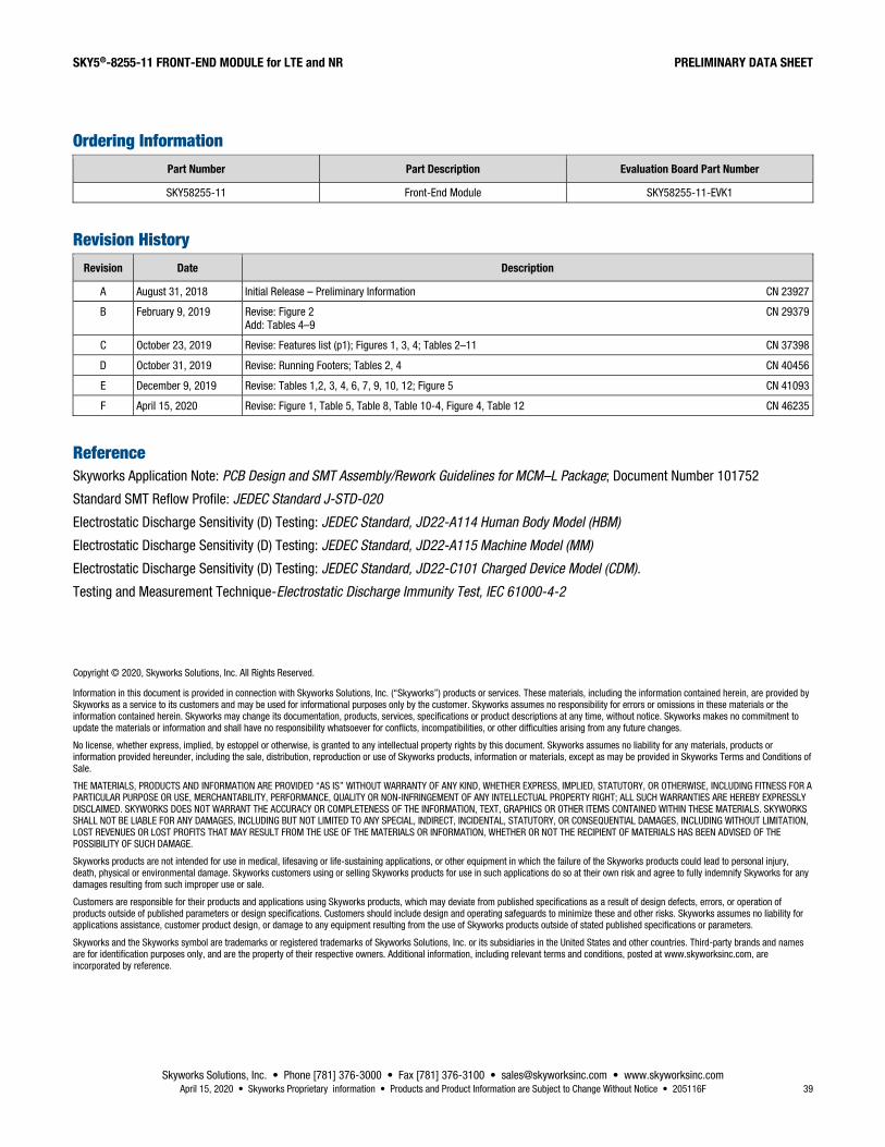
SKY5®-8255-11 FRONT-END MODULE for LTE and NR PRELIMINARY DATA SHEET
Skyworks Solutions, Inc. • Phone [781] 376-3000 • Fax [781] 376-3100 • [email protected] • www.skyworksinc.com April 15, 2020 • Skyworks Proprietary information • Products and Product Information are Subject to Change Without Notice • 205116F 39
Ordering Information
Part Number Part Description Evaluation Board Part Number
SKY58255-11 Front-End Module SKY58255-11-EVK1
Revision History
Revision Date Description
A August 31, 2018 Initial Release – Preliminary Information CN 23927
B February 9, 2019 Revise: Figure 2 CN 29379 Add: Tables 4–9
C October 23, 2019 Revise: Features list (p1); Figures 1, 3, 4; Tables 2–11 CN 37398
D October 31, 2019 Revise: Running Footers; Tables 2, 4 CN 40456
E December 9, 2019 Revise: Tables 1,2, 3, 4, 6, 7, 9, 10, 12; Figure 5 CN 41093
F April 15, 2020 Revise: Figure 1, Table 5, Table 8, Table 10-4, Figure 4, Table 12 CN 46235
Reference Skyworks Application Note: PCB Design and SMT Assembly/Rework Guidelines for MCM–L Package; Document Number 101752
Standard SMT Reflow Profile: JEDEC Standard J-STD-020
Electrostatic Discharge Sensitivity (D) Testing: JEDEC Standard, JD22-A114 Human Body Model (HBM)
Electrostatic Discharge Sensitivity (D) Testing: JEDEC Standard, JD22-A115 Machine Model (MM)
Electrostatic Discharge Sensitivity (D) Testing: JEDEC Standard, JD22-C101 Charged Device Model (CDM).
Testing and Measurement Technique-Electrostatic Discharge Immunity Test, IEC 61000-4-2
Copyright © 2020, Skyworks Solutions, Inc. All Rights Reserved.
Information in this document is provided in connection with Skyworks Solutions, Inc. (“Skyworks”) products or services. These materials, including the information contained herein, are provided by Skyworks as a service to its customers and may be used for informational purposes only by the customer. Skyworks assumes no responsibility for errors or omissions in these materials or the information contained herein. Skyworks may change its documentation, products, services, specifications or product descriptions at any time, without notice. Skyworks makes no commitment to update the materials or information and shall have no responsibility whatsoever for conflicts, incompatibilities, or other difficulties arising from any future changes.
No license, whether express, implied, by estoppel or otherwise, is granted to any intellectual property rights by this document. Skyworks assumes no liability for any materials, products or information provided hereunder, including the sale, distribution, reproduction or use of Skyworks products, information or materials, except as may be provided in Skyworks Terms and Conditions of Sale.
THE MATERIALS, PRODUCTS AND INFORMATION ARE PROVIDED “AS IS” WITHOUT WARRANTY OF ANY KIND, WHETHER EXPRESS, IMPLIED, STATUTORY, OR OTHERWISE, INCLUDING FITNESS FOR A PARTICULAR PURPOSE OR USE, MERCHANTABILITY, PERFORMANCE, QUALITY OR NON-INFRINGEMENT OF ANY INTELLECTUAL PROPERTY RIGHT; ALL SUCH WARRANTIES ARE HEREBY EXPRESSLY DISCLAIMED. SKYWORKS DOES NOT WARRANT THE ACCURACY OR COMPLETENESS OF THE INFORMATION, TEXT, GRAPHICS OR OTHER ITEMS CONTAINED WITHIN THESE MATERIALS. SKYWORKS SHALL NOT BE LIABLE FOR ANY DAMAGES, INCLUDING BUT NOT LIMITED TO ANY SPECIAL, INDIRECT, INCIDENTAL, STATUTORY, OR CONSEQUENTIAL DAMAGES, INCLUDING WITHOUT LIMITATION, LOST REVENUES OR LOST PROFITS THAT MAY RESULT FROM THE USE OF THE MATERIALS OR INFORMATION, WHETHER OR NOT THE RECIPIENT OF MATERIALS HAS BEEN ADVISED OF THE POSSIBILITY OF SUCH DAMAGE.
Skyworks products are not intended for use in medical, lifesaving or life-sustaining applications, or other equipment in which the failure of the Skyworks products could lead to personal injury, death, physical or environmental damage. Skyworks customers using or selling Skyworks products for use in such applications do so at their own risk and agree to fully indemnify Skyworks for any damages resulting from such improper use or sale.
Customers are responsible for their products and applications using Skyworks products, which may deviate from published specifications as a result of design defects, errors, or operation of products outside of published parameters or design specifications. Customers should include design and operating safeguards to minimize these and other risks. Skyworks assumes no liability for applications assistance, customer product design, or damage to any equipment resulting from the use of Skyworks products outside of stated published specifications or parameters.
Skyworks and the Skyworks symbol are trademarks or registered trademarks of Skyworks Solutions, Inc. or its subsidiaries in the United States and other countries. Third-party brands and names are for identification purposes only, and are the property of their respective owners. Additional information, including relevant terms and conditions, posted at www.skyworksinc.com, are incorporated by reference.