
Precision Triaxial Inclinometer and Accelerometer with SPI ... · Triaxial, digital inclinometer...
20
Precision Triaxial Inclinometer and Accelerometer with SPI Data Sheet ADIS16210 Rev. D Document Feedback Information furnished by Analog Devices is believed to be accurate and reliable. However, no responsibility is assumed by Analog Devices for its use, nor for any infringements of patents or other rights of third parties that may result from its use. Specifications subject to change without notice. No license is granted by implication or otherwise under any patent or patent rights of Analog Devices. Trademarks and registered trademarks are the property of their respective owners. One Technology Way, P.O. Box 9106, Norwood, MA 02062-9106, U.S.A. Tel: 781.329.4700 ©2011–2018 Analog Devices, Inc. All rights reserved. Technical Support www.analog.com FEATURES Triaxial, digital inclinometer system ±180° measurement range, roll and pitch axes ±90° gravity axis ±0.1° relative accuracy Triaxial, digital accelerometer, high accuracy ±1.7 g measurement range ±0.05° axis-to-axis alignment Digital internal temperature measurements Digital internal power supply measurements Programmable user calibration options Single command, frame alignment Manual accelerometer bias correction Programmable operation and control Sample rate/filtering Alarm conditions and indicator output Input/output: data ready, alarm, general-purpose Power management functions SPI-compatible serial interface Serial number and device ID Single-supply operation: 3.0 V to 3.6 V Calibrated temperature range: −40°C to +85°C 15 mm × 24 mm × 15 mm package with flexible connector APPLICATIONS Platform control, stabilization, and alignment Tilt sensing, inclinometers, and leveling Motion/position measurement Monitor/alarm devices (security, medical, safety) Navigation GENERAL DESCRIPTION The ADIS16210 iSensor® is a digital inclinometer system that provides precise measurements for both pitch and roll angles over a full orientation range of ±180°. It combines a MEMS tri- axial acceleration sensor with signal processing, addressable user registers for data collection/programming, and a SPI-compatible serial interface. In addition, the production process includes unit specific calibration for optimal accuracy performance. It also offers digital temperature sensor and power supply measurements together with configuration controls for in-system calibration, sample rate, filtering, alarms, input/output (I/O) configuration, and power management. The MEMS sensor elements are bound to an aluminum core for tight platform coupling and excellent mechanical stability. An internal clock drives the data sampling system, which eliminates the need for an external clock source. The SPI and data buffer structure provide convenient access to accurate sensor data and configuration controls. The ADIS16210 is available in a 15 mm × 24 mm × 15 mm module that provides mounting tabs with M2-sized mounting holes and a flexible, edge terminated connector interface. It has an extended operating temperature range of −40°C to +125°C. FUNCTIONAL BLOCK DIAGRAM ADIS16210 INCLINE CALIBRATION ALARMS I/O SELF TEST CONTROL REGISTERS SPI PORT OUTPUT REGISTERS CORRECTION AND ALIGNMENT DIGITAL FILTER TRIAXIAL MEMS SENSOR TEMPERATURE SENSOR SUPPLY POWER MANAGEMENT CS SCLK DIN DOUT GND VDD DIO1 DIO2 RST CONTROLLER 09593-001 Figure 1.
Transcript of Precision Triaxial Inclinometer and Accelerometer with SPI ... · Triaxial, digital inclinometer...

Precision Triaxial Inclinometer and Accelerometer with SPI
Data Sheet ADIS16210
Rev. D Document Feedback Information furnished by Analog Devices is believed to be accurate and reliable. However, no responsibility is assumed by Analog Devices for its use, nor for any infringements of patents or other rights of third parties that may result from its use. Specifications subject to change without notice. No license is granted by implication or otherwise under any patent or patent rights of Analog Devices. Trademarks and registered trademarks are the property of their respective owners.
One Technology Way, P.O. Box 9106, Norwood, MA 02062-9106, U.S.A. Tel: 781.329.4700 ©2011–2018 Analog Devices, Inc. All rights reserved. Technical Support www.analog.com
FEATURES Triaxial, digital inclinometer system
±180° measurement range, roll and pitch axes ±90° gravity axis ±0.1° relative accuracy
Triaxial, digital accelerometer, high accuracy ±1.7 g measurement range ±0.05° axis-to-axis alignment
Digital internal temperature measurements Digital internal power supply measurements Programmable user calibration options
Single command, frame alignment Manual accelerometer bias correction
Programmable operation and control Sample rate/filtering Alarm conditions and indicator output Input/output: data ready, alarm, general-purpose
Power management functions SPI-compatible serial interface Serial number and device ID Single-supply operation: 3.0 V to 3.6 V Calibrated temperature range: −40°C to +85°C 15 mm × 24 mm × 15 mm package with flexible connector
APPLICATIONS Platform control, stabilization, and alignment Tilt sensing, inclinometers, and leveling Motion/position measurement Monitor/alarm devices (security, medical, safety) Navigation
GENERAL DESCRIPTION The ADIS16210 iSensor® is a digital inclinometer system that provides precise measurements for both pitch and roll angles over a full orientation range of ±180°. It combines a MEMS tri-axial acceleration sensor with signal processing, addressable user registers for data collection/programming, and a SPI-compatible serial interface. In addition, the production process includes unit specific calibration for optimal accuracy performance. It also offers digital temperature sensor and power supply measurements together with configuration controls for in-system calibration, sample rate, filtering, alarms, input/output (I/O) configuration, and power management.
The MEMS sensor elements are bound to an aluminum core for tight platform coupling and excellent mechanical stability. An internal clock drives the data sampling system, which eliminates the need for an external clock source. The SPI and data buffer structure provide convenient access to accurate sensor data and configuration controls.
The ADIS16210 is available in a 15 mm × 24 mm × 15 mm module that provides mounting tabs with M2-sized mounting holes and a flexible, edge terminated connector interface. It has an extended operating temperature range of −40°C to +125°C.
FUNCTIONAL BLOCK DIAGRAM
ADIS16210
INCLINECALIBRATION
ALARMSI/OSELF TEST
CONTROLREGISTERS
SPIPORT
OUTPUTREGISTERS
CORRECTIONAND
ALIGNMENTDIGITALFILTER
TRIAXIALMEMS
SENSOR
TEMPERATURESENSOR
SUPPLY
POWERMANAGEMENT
CS
SCLK
DIN
DOUT
GND
VDDDIO1 DIO2 RST
CONTROLLER
0959
3-00
1
Figure 1.
ADIS16210 Data Sheet
Rev. D | Page 2 of 20
TABLE OF CONTENTS Features .............................................................................................. 1 Applications ....................................................................................... 1 General Description ......................................................................... 1 Functional Block Diagram .............................................................. 1 Revision History ............................................................................... 2 Specifications ..................................................................................... 3
Timing Specifications .................................................................. 4 Absolute Maximum Ratings ............................................................ 5
ESD Caution .................................................................................. 5 Pin Configuration and Function Descriptions ............................. 6 Basic Operation ................................................................................. 7
Reading Sensor Data .................................................................... 7 Device Configuration .................................................................. 7
User Register Map ............................................................................ 8 Sensor Data ........................................................................................ 9
Output Data Registers .................................................................. 9 Signal Processing, Bias Correction, and Alignment .................. 12
System Tools .................................................................................... 15 Global Commands ..................................................................... 15 Input/Output Functions ............................................................ 15 Device Identification .................................................................. 16 Status/Error Flags ....................................................................... 16 Flash Memory Management ..................................................... 16
Alarms .............................................................................................. 17 System Alarm .............................................................................. 17 Static Alarms ............................................................................... 17 Dynamic Alarms ........................................................................ 17 Alarm Reporting ........................................................................ 17
Applications Information .............................................................. 18 Mating Connector ...................................................................... 18 Breakout Board ........................................................................... 18 PC-Based Evaluation Tools ....................................................... 18
Outline Dimensions ....................................................................... 20 Ordering Guide .......................................................................... 20
REVISION HISTORY 3/2018—Rev C to Rev. D Changes to Figure 4 .......................................................................... 6 Deleted Interface Board Section, Figure 23, and Figure 25; Renumbered Sequentially .............................................................. 18 Added Breakout Board Section, PC-Based Evaluation Tools Section, and Figure 24; Renumbered Sequentially .................... 18 Added Figure 25 .............................................................................. 19 Changes to Ordering Guide .......................................................... 20
12/2016—Rev. B to Rev. C Changes to Signal Processing, Bias Correction, and Alignment Section .............................................................................................. 12
6/2015—Rev. A to Rev. B Changes to Figure 2 .......................................................................... 4 Change to Figure 5 ........................................................................... 7 Changes to User Register Map Section and Table 8 ..................... 8
Changes to Signal Processing, Bias Correction, and Alignment Section, Figure 16, and Accelerometer Bias Correction Section .. 12 Added Table 27, Table 28, and Table 29; Renumbered Sequentially ..................................................................................... 12 Changes to Table 30 and Measurement Mode Section ............. 13 Added Two-Axis Mode Section.................................................... 13 Added User Reference Alignment Section, Table 31, Table 32, and Table 33 .................................................................................... 14 Change to Table 34 ......................................................................... 15 Moved User Register Save to Flash Memory Section and Figure 20 .......................................................................................... 15 Changes to Figure 25 ...................................................................... 18
6/2011—Rev. 0 to Rev. A Changes to Table 1 ............................................................................. 3 Changes to Table 23 ....................................................................... 12 Changes to Figure 24 and Figure 25............................................. 17
4/2011—Revision 0: Initial Version

Data Sheet ADIS16210
Rev. D | Page 3 of 20
SPECIFICATIONS TA = −40°C to +85°C, VDD = 3.0 V to 3.6 V, unless otherwise noted.
Table 1. Parameter Test Conditions/Comments Min Typ Max Unit INCLINOMETERS
Measurement Range −180 +180 Degrees Relative Accuracy ±30°, AVG_CNT ≥ 0x0009, µ ± 3 σ ±0.1 Degrees ±60°, AVG_CNT ≥ 0x0009, µ ± 1 σ ±0.1 Degrees ±60°, AVG_CNT ≥ 0x0009, µ ± 3 σ ±0.15 Degrees ±180°, AVG_CNT ≥ 0x0009, µ ± 1 σ ±0.14 Degrees ±180°, AVG_CNT ≥ 0x0009, µ ± 3 σ ±0.21 Degrees Noise Density TA = 25°C, AVG_CNT = 0x0000 ±0.011 °/√Hz
ACCELEROMETERS Measurement Range ±1.7 g Offset Error µ ± 1 σ ±1 mg Sensitivity Error µ ± 1 σ ±0.0244 % Nonlinearity ±1 g, µ ± 1 σ ±1 ±2 mg Misalignment Axis to axis, deviation from 90°, µ ± 1 σ ±0.05 Degrees Noise Density TA = 25°C, AVG_CNT = 0x0000 190 µg/√Hz Bandwidth −3 dB decrease in dc sensitivity, TA = 25°C 50 Hz Sensor Resonant Frequency TA = 25°C 5.5 kHz
LOGIC INPUTS1 Input High Voltage, VINH 2.0 V Input Low Voltage, VINL 0.8 V Logic 1 Input Current, IINH VIH = 3.3 V ±0.2 ±1 µA Logic 0 Input Current, IINL VIL = 0 V
All Except RST −40 −60 µA
RST −1 mA
Input Capacitance, CIN 10 pF DIGITAL OUTPUTS1
Output High Voltage, VOH ISOURCE = 1.6 mA 2.4 V Output Low Voltage, VOL ISINK = 1.6 mA 0.4 V
FLASH MEMORY Endurance2 10,000 Cycles Data Retention3 TJ = 85°C 20 Years
START-UP TIME4 Initial Startup 156 ms Reset Recovery5 RST pulse low or Register GLOB_CMD[7] = 1 33.8 ms
Sleep Mode Recovery After CS assertion from high to low 22.3 ms
CONVERSION RATE Register AVG_CNT = 0x0000 512 SPS Clock Accuracy 3 %
POWER SUPPLY Operating voltage range, VDD 3.0 3.3 3.6 V Power Supply Current Normal mode, TA = 25°C 18 mA
Sleep mode, TA = 25°C 230 µA 1 The digital I/O signals are 5 V tolerant. 2 Endurance is qualified as per JEDEC Standard 22, Method A117, and measured at −40°C, +25°C, +85°C, and +125°C. 3 Retention lifetime equivalent at junction temperature (TJ) = 85°C as per JEDEC Standard 22, Method A117. Retention lifetime decreases with junction temperature. See
Figure 22. 4 The start-up times presented do not include the data capture time, which is dependent on the AVG_CNT register settings. 5 The RST pin must be held low for at least 15 ns.

ADIS16210 Data Sheet
Rev. D | Page 4 of 20
TIMING SPECIFICATIONS TA = 25°C, VDD = 3.3 V, unless otherwise noted.
Table 2. Parameter Description Min1 Typ Max Unit fSCLK SCLK frequency 10 830 kHz tSTALL Stall period between data, between 16th and 17th SCLK 40 μs tCS Chip select to SCLK edge 48.8 ns tDAV DOUT valid after SCLK edge 100 ns tDSU DIN setup time before SCLK rising edge 24.4 ns tDHD DIN hold time after SCLK rising edge 48.8 ns tSR SCLK rise time 12.5 ns tSF SCLK fall time 12.5 ns tDF, tDR DOUT rise/fall times 5 12.5 ns tSFS CS high after SCLK edge 5 ns 1 Guaranteed by design, not tested.
Timing Diagrams
CS
SCLK
DOUT
DIN
1 2 3 4 5 6 15 16
R/W A5A6 A4 A3 A2 D2
MSB DB14
D1 LSB
DB13 DB12 DB10DB11 DB2 LSBDB1
tCS tSFS
tDAV
tSR
tSF
tDHDtDSU
tDF, tDR
0959
3-00
2
Figure 2. SPI Timing and Sequence
CS
SCLK
tSTALL
0959
3-00
3
Figure 3. DIN Bit Sequence
Data Sheet ADIS16210
Rev. D | Page 5 of 20
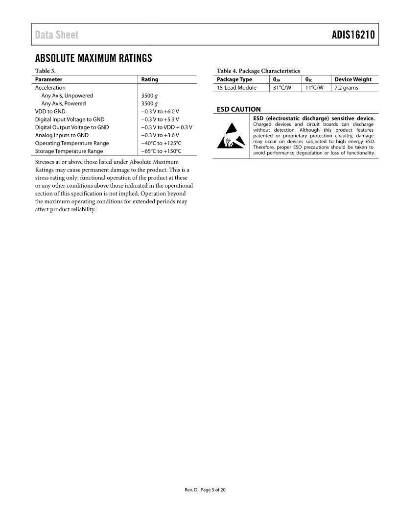
ABSOLUTE MAXIMUM RATINGS Table 3. Parameter Rating Acceleration
Any Axis, Unpowered 3500 g Any Axis, Powered 3500 g
VDD to GND −0.3 V to +6.0 V Digital Input Voltage to GND −0.3 V to +5.3 V Digital Output Voltage to GND −0.3 V to VDD + 0.3 V Analog Inputs to GND −0.3 V to +3.6 V Operating Temperature Range −40°C to +125°C Storage Temperature Range −65°C to +150°C
Stresses at or above those listed under Absolute Maximum Ratings may cause permanent damage to the product. This is a stress rating only; functional operation of the product at these or any other conditions above those indicated in the operational section of this specification is not implied. Operation beyond the maximum operating conditions for extended periods may affect product reliability.
Table 4. Package Characteristics Package Type θJA θJC Device Weight 15-Lead Module 31°C/W 11°C/W 7.2 grams
ESD CAUTION

ADIS16210 Data Sheet
Rev. D | Page 6 of 20
PIN CONFIGURATION AND FUNCTION DESCRIPTIONS
0959
3-00
4
TOP VIEW BOTTOM VIEW
PIN 15
PIN 15
PIN 1
PIN 1
NOTES1. THE LEADS ARE LOCATED ON THE BOTTOM SIDE OF THE FLEXIBLE CABLE.2. THE LEAD FINISH IS IMMERSION GOLD OVER THE ELECTROLESS NICKEL.3. THE THICKNESS OF THE GOLD FINISH IS BETWEEN 0.035µm AND 0.150µm.4. PACKAGE IS NOT SUITABLE FOR SOLDER REFLOW ASSEMBLY PROCESSES.5. EXAMPLE MATING CONNECTOR: AVX CORPORATION
FLAT FLEXIBLE CONNECTOR (FFC)P/N: 04-6288-015-000-846.
Figure 4. Pin Configuration
Table 5. Pin Function Descriptions Pin No. Mnemonic Type1 Description 1, 2 VDD S Power Supply, 3.3 V. 3, 4, 5, 8 GND S Ground. 6, 9 DNC I Do Not Connect. Do not connect to these pins. 7 DIO2 I/O Digital Input/Output Line 2. 10 RST I Reset, Active Low.
11 DIN I SPI, Data Input. 12 DOUT O SPI, Data Output. DOUT is an output when CS is low. When CS is high, DOUT is in a
three-state, high impedance mode. 13 SCLK I SPI, Serial Clock. 14 CS I SPI, Chip Select.
15 DIO1 I/O Digital Input/Output Line 1. 1 S is supply, I is input, O is output, and I/O is input/output.
Data Sheet ADIS16210
Rev. D | Page 7 of 20
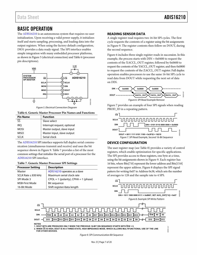
BASIC OPERATION The ADIS16210 is an autonomous system that requires no user initialization. Upon receiving a valid power supply, it initializes itself and starts sampling, processing, and loading data into the output registers. When using the factory default configuration, DIO1 provides a data ready signal. The SPI interface enables simple integration with many embedded processor platforms, as shown in Figure 5 (electrical connection) and Table 6 (processor pin descriptions).
SYSTEMPROCESSORSPI MASTER
ADIS16210
SCLK
CS
DIN
DOUT
SCLK
SS
MOSI
MISO
3.3V
IRQ DIO1
VDD
14
13
11
12
15
1 2
3 4 5 8
0959
3-00
6
Figure 5. Electrical Connection Diagram
Table 6. Generic Master Processor Pin Names and Functions Pin Name Function SS Slave select
IRQ Interrupt request, optional MOSI Master output, slave input MISO Master input, slave output SCLK Serial clock
The ADIS16210 SPI interface supports full duplex serial commu-nication (simultaneous transmit and receive) and uses the bit sequence shown in Figure 9. Table 7 provides a list of the most common settings that initialize the serial port of a processor for the ADIS16210 SPI interface.
Table 7. Generic Master Processor SPI Settings Processor Setting Description Master ADIS16210 operates as a slave SCLK Rate ≤ 830 kHz Maximum serial clock rate SPI Mode 3 CPOL = 1 (polarity), CPHA = 1 (phase) MSB-First Mode Bit sequence 16-Bit Mode Shift register/data length
READING SENSOR DATA A single register read requires two 16-bit SPI cycles. The first cycle requests the contents of a register using the bit assignments in Figure 9. The register contents then follow on DOUT, during the second sequence.
Figure 6 includes three single register reads in succession. In this example, the process starts with DIN = 0x0400 to request the contents of the XACCL_OUT register, followed by 0x0600 to request the contents of the YACCL_OUT register, and then 0x0800 to request the contents of the ZACCL_OUT register. Full duplex operation enables processors to use the same 16-bit SPI cycle to read data from DOUT while requesting the next set of data on DIN.
DIN
DOUT
0x0400 0x0600 0x0800
XACCL_OUT YACCL_OUT ZACCL_OUT
0959
3-00
7
Figure 6. SPI Read Example Remove
Figure 7 provides an example of four SPI signals when reading PROD_ID in a repeating pattern.
DOUT = 0011 1111 0101 1100 = 0x3F52 = 16210
DIN = 0101 0110 0000 0000 = 0x5600
CS
SCLK
DIN
DOUT
0959
3-00
8
Figure 7. SPI Read Example, Second 16-Bit Sequence
DEVICE CONFIGURATION The user register map (see Table 8) provides a variety of control registers, which enable optimization for specific applications. The SPI provides access to these registers, one byte at a time, using the bit assignments shown in Figure 9. Each register has 16 bits, where Bits[7:0] represent the lower address and Bits[15:8] represent the upper address. Figure 8 displays the SPI signal pattern for writing 0x07 to Address 0x38, which sets the number of averages to 128 and the sample rate to 4 SPS.
DIN = 1011 1000 0000 0111 = 0xB807, SET AVG_CNT[7:0] = 0x07
CS
SCLK
DIN
0959
3-00
9
Figure 8. Example SPI Write Pattern
0959
3-11
3
R/W R/WA6 A5 A4 A3 A2 A1 A0 DC7 DC6 DC5 DC4 DC3 DC2 DC1 DC0
D0D1D2D3D4D5D6D7D8D9D10D11D12D13D14D15
CS
SCLK
DIN
DOUT
A6 A5
D13D14D15
NOTES1. DOUT BITS ARE PRODUCED ONLY WHEN THE PREVIOUS 16-BIT DIN SEQUENCE STARTS WITH R/W = 0.2. WHEN CS IS HIGH, DOUT IS IN A THREE-STATE, HIGH IMPEDANCE MODE, WHICH ALLOWS MULTIFUNCTIONAL USE OF THE LINE
FOR OTHER DEVICES. Figure 9. SPI Communication Bit Sequence
ADIS16210 Data Sheet
Rev. D | Page 8 of 20
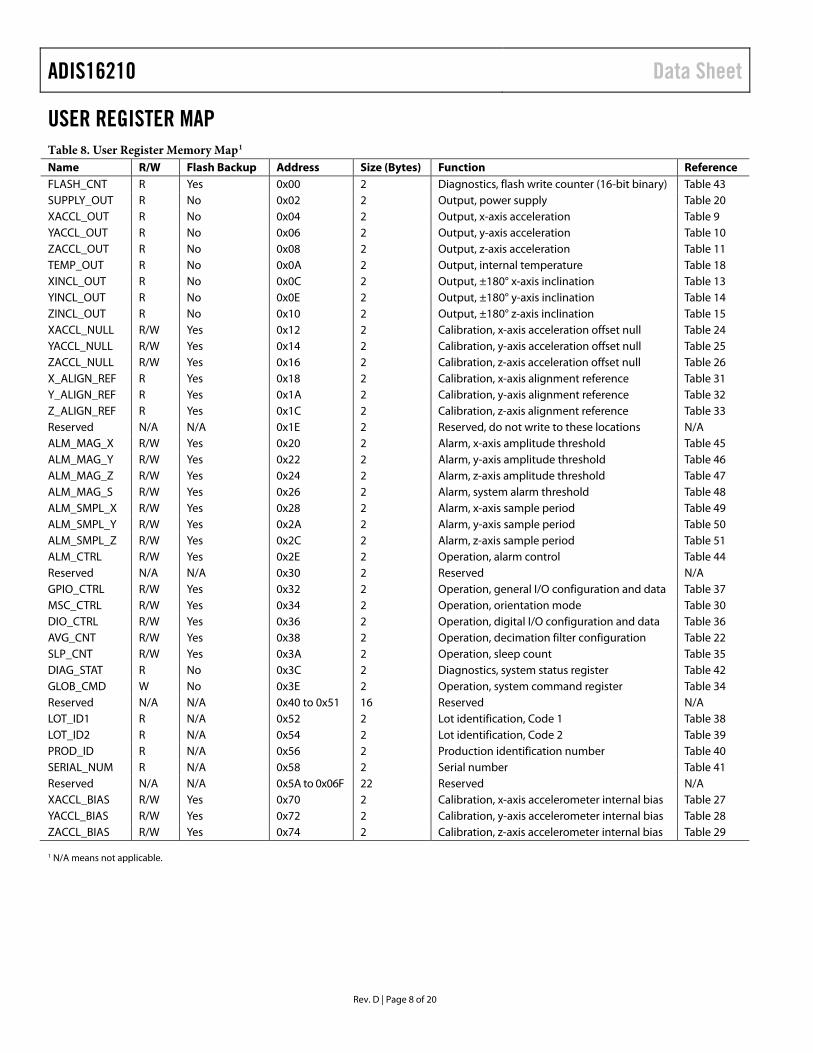
USER REGISTER MAP Table 8. User Register Memory Map1 Name R/W Flash Backup Address Size (Bytes) Function Reference FLASH_CNT R Yes 0x00 2 Diagnostics, flash write counter (16-bit binary) Table 43 SUPPLY_OUT R No 0x02 2 Output, power supply Table 20 XACCL_OUT R No 0x04 2 Output, x-axis acceleration Table 9 YACCL_OUT R No 0x06 2 Output, y-axis acceleration Table 10 ZACCL_OUT R No 0x08 2 Output, z-axis acceleration Table 11 TEMP_OUT R No 0x0A 2 Output, internal temperature Table 18 XINCL_OUT R No 0x0C 2 Output, ±180° x-axis inclination Table 13 YINCL_OUT R No 0x0E 2 Output, ±180° y-axis inclination Table 14 ZINCL_OUT R No 0x10 2 Output, ±180° z-axis inclination Table 15 XACCL_NULL R/W Yes 0x12 2 Calibration, x-axis acceleration offset null Table 24 YACCL_NULL R/W Yes 0x14 2 Calibration, y-axis acceleration offset null Table 25 ZACCL_NULL R/W Yes 0x16 2 Calibration, z-axis acceleration offset null Table 26 X_ALIGN_REF R Yes 0x18 2 Calibration, x-axis alignment reference Table 31 Y_ALIGN_REF R Yes 0x1A 2 Calibration, y-axis alignment reference Table 32 Z_ALIGN_REF R Yes 0x1C 2 Calibration, z-axis alignment reference Table 33 Reserved N/A N/A 0x1E 2 Reserved, do not write to these locations N/A ALM_MAG_X R/W Yes 0x20 2 Alarm, x-axis amplitude threshold Table 45 ALM_MAG_Y R/W Yes 0x22 2 Alarm, y-axis amplitude threshold Table 46 ALM_MAG_Z R/W Yes 0x24 2 Alarm, z-axis amplitude threshold Table 47 ALM_MAG_S R/W Yes 0x26 2 Alarm, system alarm threshold Table 48 ALM_SMPL_X R/W Yes 0x28 2 Alarm, x-axis sample period Table 49 ALM_SMPL_Y R/W Yes 0x2A 2 Alarm, y-axis sample period Table 50 ALM_SMPL_Z R/W Yes 0x2C 2 Alarm, z-axis sample period Table 51 ALM_CTRL R/W Yes 0x2E 2 Operation, alarm control Table 44 Reserved N/A N/A 0x30 2 Reserved N/A GPIO_CTRL R/W Yes 0x32 2 Operation, general I/O configuration and data Table 37 MSC_CTRL R/W Yes 0x34 2 Operation, orientation mode Table 30 DIO_CTRL R/W Yes 0x36 2 Operation, digital I/O configuration and data Table 36 AVG_CNT R/W Yes 0x38 2 Operation, decimation filter configuration Table 22 SLP_CNT R/W Yes 0x3A 2 Operation, sleep count Table 35 DIAG_STAT R No 0x3C 2 Diagnostics, system status register Table 42 GLOB_CMD W No 0x3E 2 Operation, system command register Table 34 Reserved N/A N/A 0x40 to 0x51 16 Reserved N/A LOT_ID1 R N/A 0x52 2 Lot identification, Code 1 Table 38 LOT_ID2 R N/A 0x54 2 Lot identification, Code 2 Table 39 PROD_ID R N/A 0x56 2 Production identification number Table 40 SERIAL_NUM R N/A 0x58 2 Serial number Table 41 Reserved N/A N/A 0x5A to 0x06F 22 Reserved N/A XACCL_BIAS R/W Yes 0x70 2 Calibration, x-axis accelerometer internal bias Table 27 YACCL_BIAS R/W Yes 0x72 2 Calibration, y-axis accelerometer internal bias Table 28 ZACCL_BIAS R/W Yes 0x74 2 Calibration, z-axis accelerometer internal bias Table 29 1 N/A means not applicable.

Data Sheet ADIS16210
Rev. D | Page 9 of 20
SENSOR DATA OUTPUT DATA REGISTERS The ADIS16210 provides a set of output registers for three orthogonal axes of acceleration: incline angles, internal temperature, and power supply.
Accelerometers
The accelerometers respond to both static (gravity) and dynamic acceleration using the polarity shown in Figure 10. XACCL_OUT (see Table 9), YACCL_OUT (see Table 10), and ZACCL_OUT (see Table 11) provide user access to digital calibrated accelerometer data for each axis. For example, use DIN = 0x0400 to request the x-axis data (XACCL_OUT). After reading the contents of one of these registers, convert the 16-bit, twos complement number into a decimal equivalent, and then divide that number by 16,384 to convert the measurement into units of gravity (g). Table 12 provides several examples of this data format.
Table 9. XACCL_OUT (Base Address = 0x04), Read Only Bits Description [15:0] X-axis accelerometer output data, twos complement,
1 LSB = 1 g ÷ 16,384 = ~61 µg/LSB, 0 g = 0x0000
Table 10. YACCL_OUT (Base Address = 0x06), Read Only Bits Description [15:0] Y-axis accelerometer output data, twos complement,
1 LSB = 1 g ÷ 16,384 = ~61 µg/LSB, 0 g = 0x0000
Table 11. ZACCL_OUT (Base Address = 0x08), Read Only Bits Description [15:0] Z-axis accelerometer output data, twos complement,
1 LSB = 1 g ÷ 16,384 = ~61 µg/LSB, 0 g = 0x0000
Table 12. Accelerometer Data Format Examples Orientation (g) Decimal Hex Binary +1.7 +27,853 0x6CCD 0110 1100 1100 1101 +1 +16,384 0x4000 0100 0000 0000 0000 +2/16,384 +2 0x0002 0000 0000 0000 0010 +1/16,384 +1 0x0001 0000 0000 0000 0001 0 0 0x0000 0000 0000 0000 0000 −1/16,384 −1 0xFFFF 1111 1111 1111 1111 −2/16,384 −2 0xFFFE 1111 1111 1111 1110 −1 −16,384 0xC000 1100 0000 0000 0000 −1.7 −27,853 0x9333 1001 0011 0011 0011
Inclinometers
The XINCL_OUT (see Table 13), YINCL_OUT (see Table 14), and ZINCL_OUT (see Table 15) registers provide access to incline angle data for each axis. For example, set DIN = 0x0E00 to request y-axis data (YINCL_OUT). Use the following process to translate the contents of these registers into degrees (°):
1. Convert the 16-bit, twos complement number into a decimal equivalent.
2. Multiply the decimal equivalent by 180. 3. Divide the result of Step 2 by 32,768.
Table 16 provides several examples of this data format.
Table 13. XINCL_OUT (Base Address = 0x0C), Read Only Bits Description [15:0] X-axis inclinometer output data, binary,
0° = 0x0000, 1 LSB = 180°/32,768 = ~0.0055°/LSB
Table 14. YINCL_OUT (Base Address = 0x0E), Read Only Bits Description [15:0] Y-axis inclinometer output data, binary,
0° = 0x0000, 1 LSB = 180°/32,768 = ~0.055°/LSB
Table 15. ZINCL_OUT (Base Address = 0x10), Read Only Bits Description [15:0] Z-axis inclinometer output data, binary,
0° = 0x0000, 1 LSB = 180°/32,768 = ~0.0055°/LSB
Table 16. Incline Angle Data Format Examples Orientation Decimal Hex Binary +179.9945° +32,767 0x7FFF 0111 1111 1111 1111 +0.011° +2 0x0002 0000 0000 0000 0010 +0.0055° +1 0x0001 0000 0000 0000 0001 0° 0 0x0000 0000 0000 0000 0000 −0.0055° −1 0xFFFF 1111 1111 1111 1111 −0.011° −2 0xFFFE 1111 1111 1111 1110 −180° −32,768 0x8000 1000 0000 0000 0000
Figure 10 through Figure 15 provide orientation examples and the associated output values for each accelerometer and incli-nometer register. These examples assume the factory default configuration for the gravity vector (z-axis, pointed up). See the MSC_CTRL (see Table 30) for additional options for gravity vector definitions.

ADIS16210 Data Sheet
Rev. D | Page 10 of 20
0959
3-01
2
aX
aZ
aY
Figure 10. Inclinometer Output Example, 0° Tilt 09
593-
013
aZ
aY
aX
Figure 11. Inclinometer Output Example, −30° Y-Axis Tilt
0959
3-01
6
aZ
aYaX
Figure 12. Inclinometer Output Example, −30° X-Axis Tilt
0959
3-01
4
aXa
Y
aZ
Figure 13. Inclinometer Output Example, +30° Y-Axis Tilt
0959
3-01
7
aX
aY
aZ
Figure 14. Inclinometer Output Example, +30° X-Axis Tilt
0959
3-01
5
aX
aZ
aY
Figure 15. Inclinometer Output Example, 180° Tilt
Table 17. Orientation/Output Examples for Z-Axis Gravity Orientation1
Register Figure 10 Figure 11 Figure 12 Figure 13 Figure 14 Figure 15 XACCL_OUT 0 0 −8192 0 +8192 0 YACCL_OUT 0 −8192 0 +8192 0 0 ZACCL_OUT +16,384 +14,189 +14,189 +14,189 +14,189 −16,384 XINCL_OUT 0 0 −5462 0 +5462 −32,768 YINCL_OUT 0 −5462 0 +5462 0 −32,768 ZINCL_OUT +16,384 +10,922 +10,922 +10,922 +10,922 −16,384 1 Register setting for Z-axis gravity orientation is MSC_CTRL[7:0] = xxxx xx10.
Data Sheet ADIS16210
Rev. D | Page 11 of 20
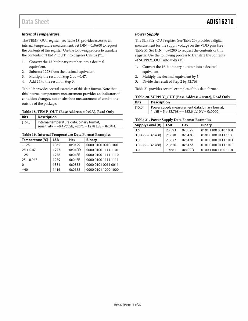
Internal Temperature
The TEMP_OUT register (see Table 18) provides access to an internal temperature measurement. Set DIN = 0x0A00 to request the contents of this register. Use the following process to translate the contents of TEMP_OUT into degrees Celsius (°C):
1. Convert the 12-bit binary number into a decimal equivalent.
2. Subtract 1278 from the decimal equivalent. 3. Multiply the result of Step 2 by −0.47. 4. Add 25 to the result of Step 3.
Table 19 provides several examples of this data format. Note that this internal temperature measurement provides an indicator of condition changes, not an absolute measurement of conditions outside of the package.
Table 18. TEMP_OUT (Base Address = 0x0A), Read Only Bits Description [15:0] Internal temperature data, binary format,
sensitivity = −0.47°/LSB, +25°C = 1278 LSB = 0x04FE
Table 19. Internal Temperature Data Format Examples Temperature (°C) LSB Hex Binary +125 1065 0x0429 0000 0100 0010 1001 25 + 0.47 1277 0x04FD 0000 0100 1111 1101 +25 1278 0x04FE 0000 0100 1111 1110 25 – 0.047 1279 0x04FF 0000 0100 1111 1111 0 1331 0x0533 0000 0101 0011 0011 −40 1416 0x0588 0000 0101 1000 1000
Power Supply
The SUPPLY_OUT register (see Table 20) provides a digital measurement for the supply voltage on the VDD pins (see Table 5). Set DIN = 0x0200 to request the contents of this register. Use the following process to translate the contents of SUPPLY_OUT into volts (V):
1. Convert the 16-bit binary number into a decimal equivalent.
2. Multiply the decimal equivalent by 5. 3. Divide the result of Step 2 by 32,768.
Table 21 provides several examples of this data format.
Table 20. SUPPLY_OUT (Base Address = 0x02), Read Only Bits Description [15:0] Power supply measurement data, binary format,
1 LSB = 5 ÷ 32,768 = ~152.6 µV, 0 V = 0x0000
Table 21. Power Supply Data Format Examples Supply Level (V) LSB Hex Binary 3.6 23,593 0x5C29 0101 1100 0010 1001 3.3 + (5 ÷ 32,768) 21,628 0x547C 0101 0100 0111 1100 3.3 21,627 0x547B 0101 0100 0111 1011 3.3 − (5 ÷ 32,768) 21,626 0x547A 0101 0100 0111 1010 3.0 19,661 0x4CCD 0100 1100 1100 1101

ADIS16210 Data Sheet
Rev. D | Page 12 of 20
SIGNAL PROCESSING, BIAS CORRECTION, AND ALIGNMENT
0959
3-02
0
3-AXISMEMS ACCEL
FACTORYCALIBRATION
ANDALIGNMENT
USERREFERENCEALIGNMENT
PITCHROLL
ANGLECALCULATION
NUMBER OF AVERAGESAVG_CNT
XACCL_OUTYACCL_OUTZACCL_OUT
XINCL_OUTYINCL_OUTZINCL_OUT
USER-ADJUSTABLE BIAS CORRECTIONXACCL_NULL, YACCL_NULL, ZACCL_NULL
USER-ADJUSTABLE BIAS CORRECTIONXACCL_BIAS, YACCL_BIAS, ZACCL_BIAS
GRAVITY AXIS DEFINITIONSELECT USING MSC_CTRL[1:0]
USER-DRIVEN ALIGNMENTCORRECTION
SET GLOB_CMD[0] = 1
Figure 16. Sensor Signal Processing Diagram (Each Axis)
The ADIS16210 provides user controls for digital filtering, accele-rometer bias correction, gravity vector definition, and the measurement mode.
Digital Filtering
The digital filter uses an averaging/decimating architecture to produce a low-pass response. The AVG_CNT register (see Table 22) provides access to the average factor, m, which determines the number of averages (N) in the filtering stage. Table 23 provides the resulting cutoff frequency (fC) and output register update rate (fS) associated with each setting in AVG_CNT.
Table 22. AVG_CNT (Base Address = 0x38), Read/Write Bits Description (Default = 0x0009) [15:4] Not used [3:0] Average factor, m, binary format Number of averages, N = 2m
Table 23. AVG_CNT Sample Rate, Bandwidth
AVG_CNT[7:0] m N fS (Output)
fC (−3 dB)
Noise (p-p)
0x0000 0 1 512 48.2 ±0.32 0x0001 1 2 256 44.6 ±0.30 0x0002 2 4 128 36.1 ±0.27 0x0003 3 8 64 23.9 ±0.22 0x0004 4 16 32 13.5 ±0.17 0x0005 5 32 16 7.0 ±0.12 0x0006 6 64 8 3.5 ±0.09 0x0007 7 128 4 1.8 ±0.06 0x0008 8 256 2 0.89 ±0.04 0x0009 9 512 1 0.44 ±0.03 0x000A 10 1024 0.5 0.22 ±0.02 0x000B 11 2048 0.25 0.11 ±0.02
Accelerometer/Inclinometer Resolution
When m (AVG_CNT[7:0] in Table 23) is between 0 and 4, the resolution in the accelerometer and inclinometer registers is equal to m + 12 bits. When m is greater than 4, the resolution in the accelerometer and inclinometer registers is 16 bits.
Accelerometer Bias Correction The XACCL_NULL (Table 24), YACCL_NULL (see Table 25), and ZACCL_NULL (see Table 26) registers add to the accel-erometer outputs to provide a bias adjustment function. They use the same format as each accelerometer output register. For example, set XACCL_NULL = 0x00F (DIN = 0x9300, 0x920F) to increase the x-axis bias by 15 LSB, or 915.5 µg (15 ÷ 16,384).
Table 24. XACCL_NULL (Base Address = 0x12), Read/Write Bits Description (Default = 0x0000) [15:0] Same format as XACCL_OUT, see Table 9
Table 25. YACCL_NULL (Base Address = 0x14), Read/Write Bits Description (Default = 0x0000) [15:0] Same format as YACCL_OUT, see Table 10
Table 26. ZACCL_NULL (Base Address = 0x16), Read/Write Bits Description (Default = 0x0000) [15:0] Same format as ZACCL_OUT, see Table 11
The XACCL_BIAS (see Table 27), YACCL_BIAS (see Table 28), and ZACCL_BIAS (see Table 34) registers add to the accelerometer signals, prior to the angle computation function.
Table 27. XACCL_BIAS (Base Address = 0x70), Read/Write Bits Description (Default = 0x0000) [15:0] Same format as XACCL_OUT, see Table 9
Table 28. YACCL_BIAS (Base Address = 0x72), Read/Write Bits Description (Default = 0x0000) [15:0] Same format as YACCL_OUT, see Table 10
Table 29. ZACCL_BIAS (Base Address = 0x74), Read/Write Bits Description (Default = 0x0000) [15:0] Same format as ZACCL_OUT, see Table 11
Data Sheet ADIS16210
Rev. D | Page 13 of 20
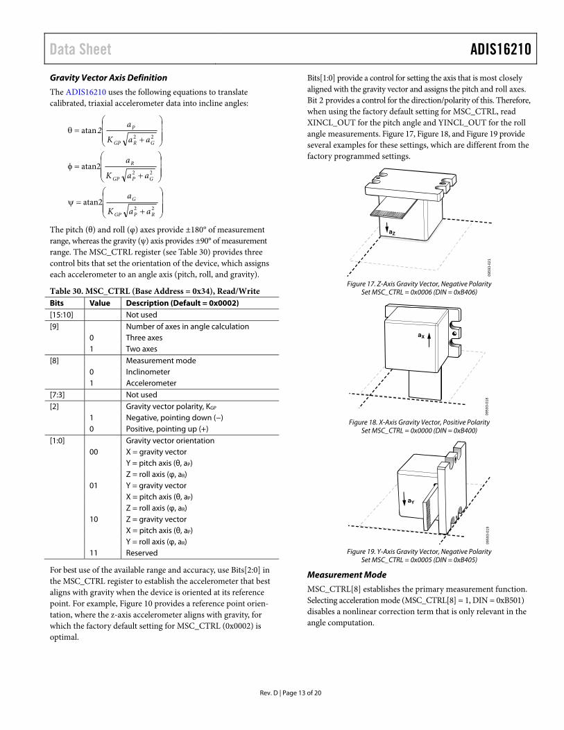
Gravity Vector Axis Definition
The ADIS16210 uses the following equations to translate calibrated, triaxial accelerometer data into incline angles:
22
22
22
atan2
atan2
atan
RPGP
G
GPGP
R
GRGP
P
aaK
a
aaK
a
aaK
a2
The pitch (θ) and roll (φ) axes provide ±180° of measurement range, whereas the gravity (ψ) axis provides ±90° of measurement range. The MSC_CTRL register (see Table 30) provides three control bits that set the orientation of the device, which assigns each accelerometer to an angle axis (pitch, roll, and gravity).
Table 30. MSC_CTRL (Base Address = 0x34), Read/Write Bits Value Description (Default = 0x0002) [15:10] Not used [9] Number of axes in angle calculation 0 Three axes 1 Two axes [8] Measurement mode 0 Inclinometer 1 Accelerometer [7:3] Not used [2] Gravity vector polarity, KGP 1 Negative, pointing down (−) 0 Positive, pointing up (+) [1:0] Gravity vector orientation 00 X = gravity vector Y = pitch axis (θ, aP) Z = roll axis (φ, aR) 01 Y = gravity vector X = pitch axis (θ, aP) Z = roll axis (φ, aR) 10 Z = gravity vector X = pitch axis (θ, aP) Y = roll axis (φ, aR) 11 Reserved
For best use of the available range and accuracy, use Bits[2:0] in the MSC_CTRL register to establish the accelerometer that best aligns with gravity when the device is oriented at its reference point. For example, Figure 10 provides a reference point orien-tation, where the z-axis accelerometer aligns with gravity, for which the factory default setting for MSC_CTRL (0x0002) is optimal.
Bits[1:0] provide a control for setting the axis that is most closely aligned with the gravity vector and assigns the pitch and roll axes. Bit 2 provides a control for the direction/polarity of this. Therefore, when using the factory default setting for MSC_CTRL, read XINCL_OUT for the pitch angle and YINCL_OUT for the roll angle measurements. Figure 17, Figure 18, and Figure 19 provide several examples for these settings, which are different from the factory programmed settings.
0959
3-02
1
aZ
Figure 17. Z-Axis Gravity Vector, Negative Polarity
Set MSC_CTRL = 0x0006 (DIN = 0xB406)
0959
3-01
8
aX
Figure 18. X-Axis Gravity Vector, Positive Polarity
Set MSC_CTRL = 0x0000 (DIN = 0xB400)
0959
3-01
9
aY
Figure 19. Y-Axis Gravity Vector, Negative Polarity
Set MSC_CTRL = 0x0005 (DIN = 0xB405)
Measurement Mode
MSC_CTRL[8] establishes the primary measurement function. Selecting acceleration mode (MSC_CTRL[8] = 1, DIN = 0xB501) disables a nonlinear correction term that is only relevant in the angle computation.

ADIS16210 Data Sheet
Rev. D | Page 14 of 20
Two-Axis Mode
In cases where two-axis computations are preferred, set MSC_CTRL[9] = 1 (DIN = 0xB502). This simplifies the pitch and roll equations to the following:
×
=
×
=
GGP
R
GGP
P
aKa
aKa2
atan2
atan
φ
θ
User Reference Alignment
Set GLOB_CMD[0] = 1 (DIN = 0xBE01) to trigger the user reference alignment function, which observes the accelerometer values and computes a rotation matrix that reorients them to the reference frame definition, per the settings in MSC_CTRL[2:0]. For example, when using the default setting for these bits, executing this command remaps the accelerometers to the following values: XACCL_OUT = 0 g, YACCL_OUT = 0 g and ZACCL_OUT = 1 g.
The initial accelerometer readings, prior to the alignment process, are available in the X_ALIGN_REF (see Table 31), Y_ALIGN_REF (see Table 32), and Z_ALIGN_REF (see Table 33) registers.
Table 31. X_ALIGN_REF (Base Address = 0x18), Read/Write Bits Description (Default = 0x0000) [15:0] Same format as XACCL_OUT, see Table 9
Table 32. Y_ALIGN_REF (Base Address = 0x1A), Read/Write Bits Description (Default = 0x0000) [15:0] Same format as YACCL_OUT, see Table 10
Table 33. Z_ALIGN_REF (Base Address = 0x1C), Read/Write Bits Description (Default = 0x0000) [15:0] Same format as ZACCL_OUT, see Table 11
Data Sheet ADIS16210
Rev. D | Page 15 of 20
SYSTEM TOOLS The ADIS16210 provides control registers for the following system level functions: global commands (including self test), input/output functions, device identification, status/error flags, and flash memory management.
GLOBAL COMMANDS The GLOB_CMD register (see Table 34) provides an array of single write commands. Set the assigned bit to 1 to activate each function. Proper execution of each command depends on the power supply being within normal limits and no SPI communication, during the process times listed in Table 34.
Table 34. GLOB_CMD (Base Address = 0x3E), Write Only Bits Description Process Time1 [15:8] Not used Not applicable [7] Software reset 33.7 ms [6] User register save to flash memory 28.0 ms [5] Flash memory test 31.3 ms [4] Clear DIAG_STAT register 93 µs [3] Restore factory default configuration 68.6 ms [2] Self test 53.7 ms [1] Power-down Not applicable [0] User reference alignment Not applicable
1 This indicates the typical duration of time between the command write and the device returning to normal operation.
Software Reset
Set GLOB_CMD[7] = 1 (DIN = 0xBE80) to execute an internal reset, which flushes all data and restores the register values to the values that are stored in nonvolatile flash memory.
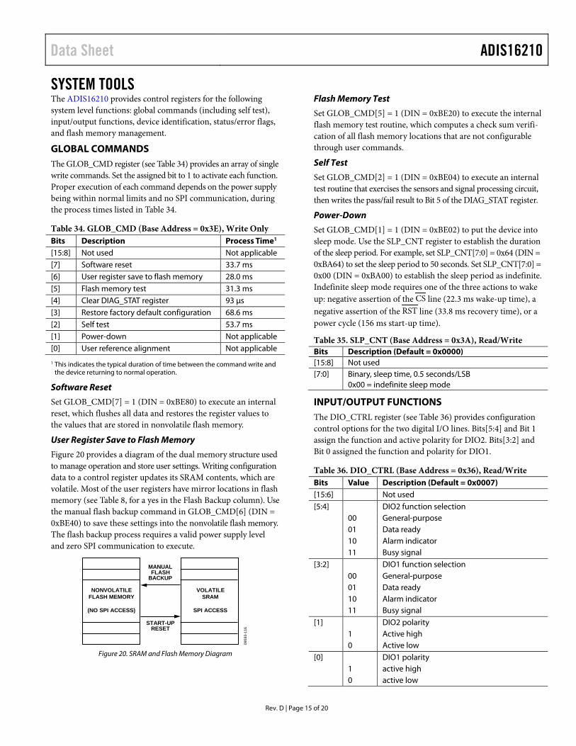
User Register Save to Flash Memory
Figure 20 provides a diagram of the dual memory structure used to manage operation and store user settings. Writing configuration data to a control register updates its SRAM contents, which are volatile. Most of the user registers have mirror locations in flash memory (see Table 8, for a yes in the Flash Backup column). Use the manual flash backup command in GLOB_CMD[6] (DIN = 0xBE40) to save these settings into the nonvolatile flash memory. The flash backup process requires a valid power supply level and zero SPI communication to execute.
NONVOLATILEFLASH MEMORY
(NO SPI ACCESS)
MANUALFLASH
BACKUP
START-UPRESET
VOLATILESRAM
SPI ACCESS
0959
3-11
6
Figure 20. SRAM and Flash Memory Diagram
Flash Memory Test
Set GLOB_CMD[5] = 1 (DIN = 0xBE20) to execute the internal flash memory test routine, which computes a check sum verifi-cation of all flash memory locations that are not configurable through user commands.
Self Test
Set GLOB_CMD[2] = 1 (DIN = 0xBE04) to execute an internal test routine that exercises the sensors and signal processing circuit, then writes the pass/fail result to Bit 5 of the DIAG_STAT register.
Power-Down
Set GLOB_CMD[1] = 1 (DIN = 0xBE02) to put the device into sleep mode. Use the SLP_CNT register to establish the duration of the sleep period. For example, set SLP_CNT[7:0] = 0x64 (DIN = 0xBA64) to set the sleep period to 50 seconds. Set SLP_CNT[7:0] = 0x00 (DIN = 0xBA00) to establish the sleep period as indefinite. Indefinite sleep mode requires one of the three actions to wake up: negative assertion of the CS line (22.3 ms wake-up time), a negative assertion of the RST line (33.8 ms recovery time), or a power cycle (156 ms start-up time).
Table 35. SLP_CNT (Base Address = 0x3A), Read/Write Bits Description (Default = 0x0000) [15:8] Not used [7:0] Binary, sleep time, 0.5 seconds/LSB
0x00 = indefinite sleep mode
INPUT/OUTPUT FUNCTIONS The DIO_CTRL register (see Table 36) provides configuration control options for the two digital I/O lines. Bits[5:4] and Bit 1 assign the function and active polarity for DIO2. Bits[3:2] and Bit 0 assigned the function and polarity for DIO1.
Table 36. DIO_CTRL (Base Address = 0x36), Read/Write Bits Value Description (Default = 0x0007) [15:6] Not used [5:4] DIO2 function selection 00 General-purpose 01 Data ready 10 Alarm indicator 11 Busy signal [3:2] DIO1 function selection 00 General-purpose 01 Data ready 10 Alarm indicator 11 Busy signal [1] DIO2 polarity 1 Active high 0 Active low [0] DIO1 polarity 1 active high 0 active low

ADIS16210 Data Sheet
Rev. D | Page 16 of 20
Data Ready Indicator
The data ready signal pulses to its inactive state when loading fresh data into the output registers, then back to its active state when the register update process completes, as shown in Figure 21, which shows the factory default operation. Set DIO_CTRL[7:0] = 0x13 (DIN = 0xB613) to change the data ready assignment to DIO2 with a positive polarity.
0959
3-02
3
ACTIVE INACTIVEDIO1
Figure 21. Data Ready Operation, DIO_CTRL[7:0] = 0x05
Alarm Indicator
Set DIO_CTRL[7:0] = 0x27 (DIN = 0xB627) to configure DIO2 as an alarm indicator with an active high polarity. The alarm indicator transitions to its active state when the acceleration or system data exceeds the threshold settings in the ALM_MAG_x registers. Set GLOB_CMD[4] = 1 (DIN = 0xBF10) to clear the DIAG_STAT error flags and restore the alarm indicator to its inactive state.
General-Purpose Input/Output
If DIO_CTRL configures either DIO1 or DIO2 as a general-purpose digital line, use the GPIO_CTRL register (see Table 37) to configure its input/output direction, set the output level when configured as an output, and monitor the status of an input. For example, set DIO_CTRL[3:0] = 0x00 (DIN = 0xB600) to establish DIO1 as a general-purpose line, set GPIO_CTRL[0] = 1 (DIN = 0xB201) to establish DIO1 as an output, and set GPIO_CTRL[8] = 1 (DIN = 0xB301) to set DIO1 high.
Table 37. GPIO_CTRL (Base Address = 0x32), Read/Write Bits Description (Default = 0x0000) [15:10] Not used [9] DIO2 output level, 1 = high, 0 = low [8] DIO1 output level, 1 = high, 0 = low [7:2] Reserved [1] DIO2 direction control, 1 = output, 0 = input [0] DIO1 direction control, 1 = output, 0 = input
DEVICE IDENTIFICATION Table 38. LOT_ID1 (Base Address = 0x52), Read Only Bits Description [15:0] Lot identification code
Table 39. LOT_ID2 (Base Address = 0x54), Read Only Bits Description [15:0] Lot identification code
Table 40. PROD_ID (Base Address = 0x56), Read Only Bits Description (Default = 0x3F52) [15:0] 0x3F52 = 16,210
Table 41. SERIAL_NUM (Base Address = 0x58), Read Only Bits Description [15:0] Serial number, lot specific
STATUS/ERROR FLAGS The DIAG_STAT register, in Table 42, provides a number of status/error flags that reflect the conditions observed during a capture, during SPI communication and diagnostic tests. A 1 indicates an error condition and all of the error flags are sticky, which means that they remain until they are reset by setting GLOB_CMD[4] = 1 (DIN = 0xBE10). The flag in Bit 3 of the DIAG_STAT register indicates that the total number of SCLK clocks is not a multiple of 16. Set DIN = 0x3C00 to read this register.
Table 42. DIAG_STAT (Base Address = 0x3C), Read Only Bits Description (Default = 0x0000) [15:12] Not used [11] Alarm S flag [10] Alarm Z flag [9] Alarm Y flag [8] Alarm X flag [7] Data ready [6] Flash test [5] Self test [4] Not used [3] SPI failure [2] Flash update failure [1] VDD > 3.625 [0] VDD < 2.975
FLASH MEMORY MANAGEMENT Set GLOB_CMD[5] = 1 (DIN = 0xBE20) to run an internal check-sum test on the flash memory, which reports a pass/fail result to DIAG_STAT[6]. The FLASH_CNT register (see Table 43) provides a running count of flash memory write cycles. This is a tool for managing the endurance of the flash memory. Figure 22 quantifies the relationship between data retention and junction temperature.
Table 43. FLASH_CNT (Base Address = 0x00), Read Only Bits Description [15:0] Binary counter for writing to flash memory
600
450
300
150
030 40
RET
ENTI
ON
(Yea
rs)
JUNCTION TEMPERATURE (°C)55 70 85 100 125 135 150
0959
3-11
5
Figure 22. Flash/EE Memory Data Retention

Data Sheet ADIS16210
Rev. D | Page 17 of 20
ALARMS There are four independent alarms, which provide trigger level and polarity controls. The ALM_CTRL register (see Table 44) provides individual settings for data source selection (Bits[7:4]), static and dynamic comparison (Bits[14:12]), trigger direction/ polarity (Bits[11:8]), and alarm enable (Bits[3:0]).
Table 44. ALM_CTRL (Base Address = 0x2E), Read/Write Bits Description (Default = 0x0000) [15] Not used [14] Alarm Z, dynamic control 1 = dynamic, 0 = static [13] Alarm Y, dynamic control 1 = dynamic, 0 = static [12] Alarm X, dynamic control 1 = dynamic, 0 = static [11] Alarm S, comparison polarity 1 = SUPPLY_OUT/TEMP_OUT > ALM_MAG_S 0 = SUPPLY_OUT/TEMP_OUT < ALM_MAG_S [10] Alarm Z, comparison polarity 1 = ZACCL_OUT/ZINCL_OUT > ALM_MAG_Z 0 = ZACCL_OUT/ZINCL_OUT < ALM_MAG_Z [9] Alarm Y, comparison polarity 1 = YACCL_OUT/YINCL_OUT > ALM_MAG_Y 0 = YACCL_OUT/YINCL_OUT < ALM_MAG_Y [8] Alarm X, comparison polarity 1 = XACCL_OUT/XINCL_OUT > ALM_MAG_X 0 = XACCL_OUT/XINCL_OUT < ALM_MAG_X [7] Alarm S, source selection 1 = SUPPLY_OUT, 0 = TEMP_OUT [6] Alarm Z, source selection 1 = ZINCL_OUT, 0 = ZACCL_OUT [5] Alarm Y, source selection 1 = YINCL_OUT, 0 = YACCL_OUT [4] Alarm X, source selection 1 = XINCL_OUT, 0 = XACCL_OUT [3] Alarm S, enable 1 = enabled, 0 = disabled [2] Alarm Z, enable 1 = enabled, 0 = disabled [1] Alarm Y, enable 1 = enabled, 0 = disabled [0] Alarm X, enable 1 = enabled, 0 = disabled
SYSTEM ALARM The system alarm monitors either power supply or internal tem-perature, according to the user selections in ALM_CTRL[11], ALM_CTRL[7], ALM_CTRL[3], and the ALM_MAG_S register in Table 48. For example, set ALM_CTRL = 0x0008 (DIN = 0xA900, 0xA808) and ALM_MAG_S = 0x533 (DIN = 0xA705, 0xA633) to disable all three inertial alarms and configure the system alarm active when TEMP_OUT is <0°C.
STATIC ALARMS The static alarm setting enables the ADIS16210 to compare the data source (ALM_CTRL[6:4]) with the corresponding values
in the ALM_MAG_x registers (see Table 45, Table 46, and Table 47) using the trigger direction/polarity settings in ALM_CTRL[10:8]. For example, if ALM_CTRL[10] = 0, ALM_CTRL[6] = 1, and ALM_MAG_Z = 0x2000, then Alarm Z becomes active when ZINCL_OUT is less than 0x2000, or 45°.
DYNAMIC ALARMS The dynamic alarm setting monitors the data selection for a rate-of-change comparison. The rate-of-change comparison is represented by the magnitude in the ALM_MAG_x registers (see Table 45, Table 46, and Table 47), divided by the time in the ALM_SMPL_x registers (see Table 49, Table 50, Table 51).
For example, if ALM_CTRL[9] = 1, ALM_CTRL[5] = 0, ALM_MAG_Y = 0x4000, and ALM_SMPL_Y = 0x0064, then Alarm Y (DIAG_STAT[9]) becomes active when YACCL_OUT changes by more than +1 g over 100 samples. The AVG_CNT register (Table 22) establishes the time for each sample.
Table 45. ALM_MAG_X (Base Address = 0x20), Read/Write Bits Description (Default = 0x0000) [15:0] Same data format as ZACCL_OUT or ZINCL_OUT,
according to the setting in ALM_CTRL[4]
Table 46. ALM_MAG_Y (Base Address = 0x22), Read/Write Bits Description (Default = 0x0000) [15:0] Same data format as ZACCL_OUT or ZINCL_OUT,
according to the setting in ALM_CTRL[5]
Table 47. ALM_MAG_Z (Base Address = 0x24), Read/Write Bits Description (Default = 0x0000) [15:0] Same data format as ZACCL_OUT or ZINCL_OUT,
according to the setting in ALM_CTRL[6]
Table 48. ALM_MAG_S (Base Address = 0x26), Read/Write Bits Description (Default = 0x0000) [15:0] Same data format as SUPPLY_OUT or TEMP_OUT,
according to the setting in ALM_CTRL[7]
Table 49. ALM_SMPL_X (Base Address = 0x28), Read/Write Bits Description (Default = 0x0001) [15:8] Not used [7:0] Binary, number of samples
Table 50. ALM_SMPL_Y (Base Address = 0x2A), Read/Write Bits Description (Default = 0x0001) [15:8] Not used [7:0] Binary, number of samples
Table 51. ALM_SMPL_Z (Base Address = 0x2C), Read/Write Bits Description (Default = 0x0001) [15:8] Not used [7:0] Binary, number of samples
ALARM REPORTING See DIAG_STAT[11:8] (see Table 42) for alarm flags, which equal 1 when an alarm condition is detected. DIO_CTRL (see Table 36) offers settings that configure DIO1 or DIO2 as an alarm indicator signal.
ADIS16210 Data Sheet
Rev. D | Page 18 of 20
APPLICATIONS INFORMATION MATING CONNECTOR The mating connector for the ADIS16210, J2, is the AVX® 04-6288-015-000-846. Figure 23 provides a close-up view of this connector, which clamps down on the flex cable to press its metal pads onto the metal pads inside of the mating connector.
0959
3-20
0
MATINGCONNECTOR
SLIDER
SLIDERLOCKING
DIRECTION
ADIS16210FLEX CABLE
Figure 23. Mating Connector Detail
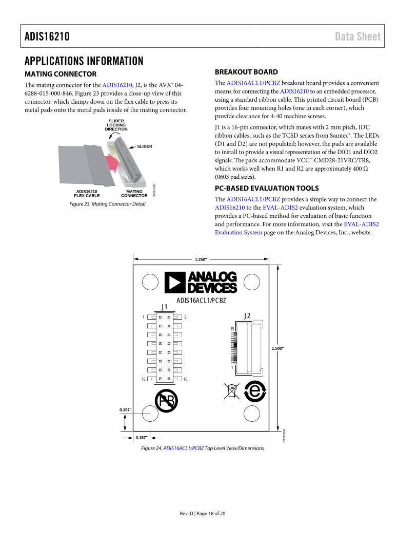
BREAKOUT BOARD The ADIS16ACL1/PCBZ breakout board provides a convenient means for connecting the ADIS16210 to an embedded processor, using a standard ribbon cable. This printed circuit board (PCB) provides four mounting holes (one in each corner), which provide clearance for 4-40 machine screws.
J1 is a 16-pin connector, which mates with 2 mm pitch, IDC ribbon cables, such as the TCSD series from Samtec®. The LEDs (D1 and D2) are not populated; however, the pads are available to install to provide a visual representation of the DIO1 and DIO2 signals. The pads accommodate VCC™ CMD28-21VRC/TR8, which works well when R1 and R2 are approximately 400 Ω (0603 pad sizes).
PC-BASED EVALUATION TOOLS The ADIS16ACL1/PCBZ provides a simple way to connect the ADIS16210 to the EVAL-ADIS2 evaluation system, which provides a PC-based method for evaluation of basic function and performance. For more information, visit the EVAL-ADIS2 Evaluation System page on the Analog Devices, Inc., website.
0959
3-02
6
1.500"
0.157"
0.157"
1.250"
J11 2
15 16
J2
ADIS16ACL1/PCBZ
1
15
Figure 24. ADIS16ACL1/PCBZ Top Level View/Dimensions

Data Sheet ADIS16210
Rev. D | Page 19 of 20
1 2
J1123456789
101112131415
04-6288-015-000-846
ADIS16210/ADIS16228 PACKAGE PIN OUT
J2J1
3 45 67 89 10
11 1213 1415 16
SPAREPIN
SPAREPIN
SPAREPIN
A3-16PA-2SV (71)
VDD
DGND DGND
DGND DGND
RSTCS
DIO1
SCLKDOUT
DIO2
DIN
D1
CMD28-21VRC/TR8 (RED)A C
R1400Ω
D2
CMD28-21VRC/TR8 (RED)A C
R2400Ω
DGND
VDD
C110µF
C20603DNI
VDD
DIO2
RSTDIN
DOUTSCLK
CSDIO1
SPAREPIN
SPAREPIN
0959
3-02
7
Figure 25. ADIS16ACL1/PCBZ Electrical Schematic
ADIS16210 Data Sheet
Rev. D | Page 20 of 20
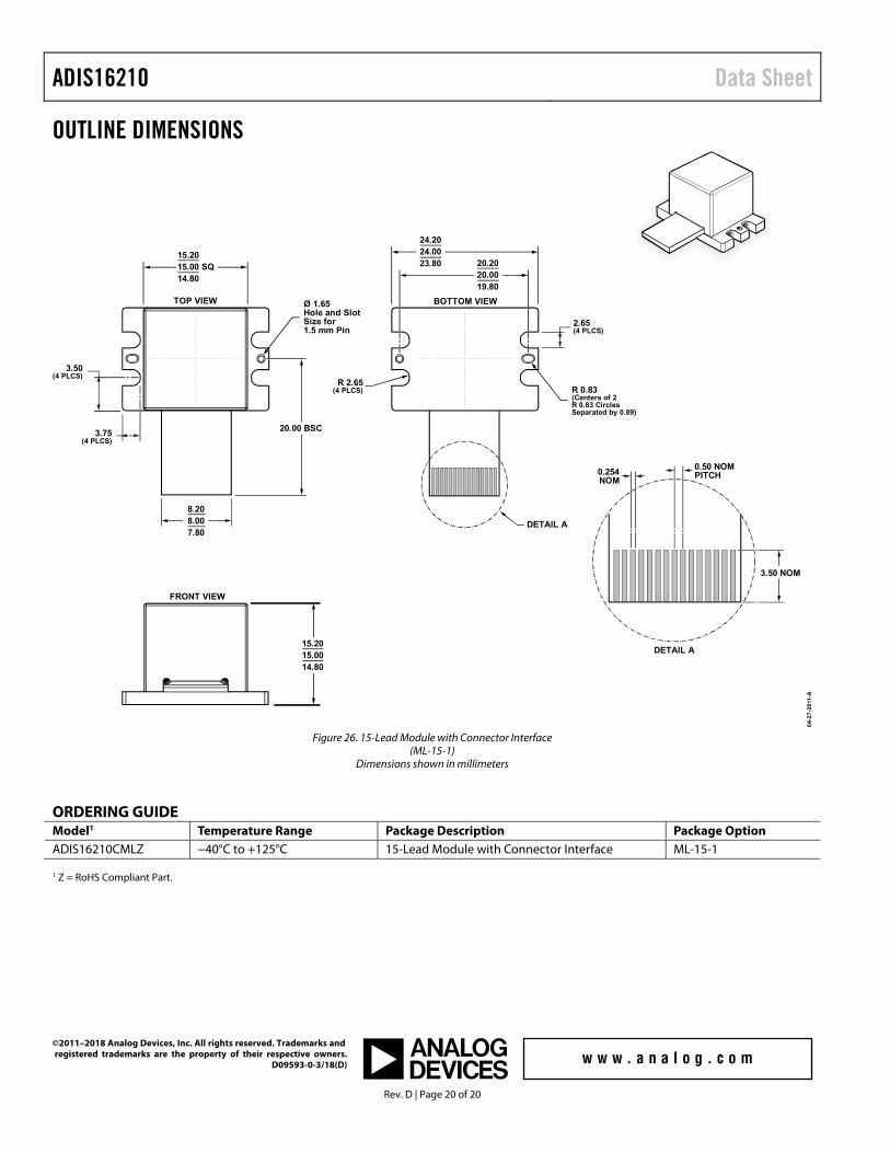
OUTLINE DIMENSIONS
04-
27
-20
11-A
15.2015.00 SQ14.80
24.2024.0023.80 20.20
20.0019.80
TOP VIEW BOTTOM VIEW
20.00 BSC3.75
(4 PLCS)
R 2.65(4 PLCS)
2.65(4 PLCS)
3.50(4 PLCS)
DETAIL A
FRONT VIEW
15.2015.0014.80
8.208.007.80
Ø 1.65Hole and SlotSize for1.5 mm Pin
R 0.83(Centers of 2R 0.83 CirclesSeparated by 0.89)
0.50 NOMPITCH
3.50 NOM
0.254NOM
DETAIL A
Figure 26. 15-Lead Module with Connector Interface (ML-15-1)
Dimensions shown in millimeters
ORDERING GUIDE Model1 Temperature Range Package Description Package Option ADIS16210CMLZ −40°C to +125°C 15-Lead Module with Connector Interface ML-15-1
1 Z = RoHS Compliant Part.
©2011–2018 Analog Devices, Inc. All rights reserved. Trademarks and registered trademarks are the property of their respective owners.
D09593-0-3/18(D)