Precision Materials Processing - logitech.uk.com · The CP3000 and CP4000 systems offer processing...
20
Complete Systems for Precision Materials Processing www.logitech.uk.com
Transcript of Precision Materials Processing - logitech.uk.com · The CP3000 and CP4000 systems offer processing...

Complete Systems for
Precision Materials Processing
www.logitech.uk.com

2
IntroductionAbout UsLogitech Limited has many years of experience in advanced materials processing. Our forward thinking company originated as a spin-out business from University of Glasgow, Scotland in 1965.
Having gone from strength to strength Logitech is a world leader in its field and is respected for its professional expertise, quality products and services within many aspects of materials shaping and surface finishing technology.
We have our head office, manufacturing plant and training facilities in Glasgow. The team of highly skilled designers, engineers, technical sales, quality assurance and support staff work across the globe, providing state-of-the-art products, services and training to key market sectors and our client base.
Nature of our BusinessWe operate within materials processing and supported industries, designing and manufacturing a range of precision sawing, lapping and polishing equipment.
Our global client base includes; industry, academia and government agencies with a need for high specification surface finishes, prepared with precise geometric accuracy. Key markets include semiconductor materials, opto-electronics, optics and geological sciences.
Trading PhilosophyOur company is driven by client satisfaction and the ability to obtain maximum results from our products and services. Through the provision of “system packages” which include technology transfer, we provide reliable systems that meet your specifications over a long period of time. This is achieved through:
• market-orientated design • precision-engineered and high quality manufactured products • access to considerable in-house materials processing expertise • highly valued after-sale support
Our know-how and highly respected products and services are developed by using our market knowledge, and actively listening to our client needs. We remain committed to positive interaction with all of our clients, both directly and through a worldwide network of distributors.
Environmental CommitmentWe maintain a proactive approach to ensure any releases to air, land and water are both monitored and controlled to meet the Environmental Protection Act (1990). We manage this through strict controls and the use of alternative products and processes, where viable. Ensuring both the risk of damaging releases and the damage arising from such releases are minimised as far as practicable. In this endeavour Logitech considers it has an equal obligation to internal, local and global environmental concerns.

3
ContentsPage 4 Semiconductor Materials Wafer slicing, standard backlapping or polishing of III-V and II-VI wafers down to 50µm or less with accuracies of 2µm. Electronic grade surface finishes or low sub-surface damage chemical polishing. Hard Materials Processing and Chemical Mechanical Processing (CMP).
Page 6 Opto-electronics Preparation of substrates of all types of opto-electronic, electro-optic and acousto-optic materials with scratch free faces, defect free edges, and with precise dimensions.
Page 8 Optics Polishing of laser windows, mirrors and rods, manufacture or reclaim of Q-switches, optical prisms, chalcogenide glass, general optical polishing of any material to λ/10 with angular accuracies of 2 seconds of arc or better.
Page 10 Geological Sciences Lapping and polishing of thin or ultra-thin sections of rocks, refractory, concrete, soils.
Page 12 Other Applications Fine lap/polish of virtually any material to diverse optical tolerance geometries: ceramics, metals and alloys, tooth, bone, recording heads, hygroscopic crystals, plastics, and many more.
Page 14 Test & Measurement Equipment to complement machine systems, including thickness measurement gauges, interferometers, and autocollimators.
Page 15 Accessories Wide selection of precision lapping and polishing jigs, pads and cloths for optimum results.
Page 16 Consumable Products A high quality range of products, such as abrasive powders, waxes, saw blades and microscope slides, ensure the best in sample processing performance.
Page 18 Technology Transfer Comprehensive training to develop your application process, maximise system operation and undertake maintenance.
Page 19 Customer Support Our dedication to after sales support and continuous improvement.

4
Semiconductor
Lapping and PolishingOur core business is lapping and polishing machines for highly accurate and controlled material removal and preparation of the sample surface. Our systems are supplied to suit all semiconductor materials and related processes.
The reliable PM5 and LP50 precision lapping and polishing systems are key Logitech products, with over 1500 currently installed in client premises worldwide. The PM5 is a single workstation unit whilst the LP50 supports up to three processing jigs simultaneously. Both systems are designed to be flexible, robust and intuitive to use. The principals that we employ for lapping is to control the supply of abrasive slurry, that is held in liquid suspension, to a revolving lapping plate. A precision jig is placed on to the plate, to correctly orient the sample and control the pressure applied. This ensures the material removal is uniform and samples meet expectation in terms of flatness, parallelism, etc. The lapping process imparts less stress on the wafer and produces less surface and sub-surface damage, compared to techniques such as grinding or fixed abrasive pads.
A range of jigs and fixtures can be supplied to cater for different samples, whilst many options are available on the PM5 and LP50 systems to meet your requirements.
The PM5 and LP50 systems can be used for both lapping and polishing, with easy changover between the two processes. Both machines are available to use with sodium hypochlorite based polishing solutions. The Logitech single station DL1 or four workstation DL4 are premium systems for lapping of soft materials.
Chemical PolishingWhere epitaxial growth is required on the semiconductor wafer, the surface can be prepared using Logitech chemical polishing equipment. The CP3000 and CP4000 systems offer processing of a range of sample sizes. The CP3000 is designed for use in an existing fume cabinet, whilst the CP4000 comes with the fume enclosure included.
Chemical Mechanical Processing (CMP)
We have developed a number of dedicated CMP tools, culminating in the Tribo and Orbis units. These machines manipulate the wafer shape and have high levels of control over parameters such as download backpressure, solution flow and rotational speed. The highest levels of surface finish and flatness on samples are possible with these systems.
Primary applications for the Tribo and Orbis systems are delayering and planarisation, with secondary applications in the field of tribological science and research.
The chemically resistant systems process part and full wafers up to 4” on the Tribo system and 8” on the Orbis system.
Hard Materials Processing
Logitech PM5 and LP50 systems are capable of processing hard materials such as sapphire, galium nitride and silicon carbide up to 4” diameter. Whilst our driven head range of tools provide better processing cycle times and real time measurement with data collection. The driven lapping (DL) and driven polishing (DP) tools have added control over the movement of the jig or processing head, as well as the ability to produce high levels of downforce when polishing. The DL and DP machines are capable of processing multiple samples, helping to reduce time per sample.
The DL and DP machines are available in either a single workstation (DL1, DP1) or four workstation (DL4 and DP4) model. Control over the machines is via a touchscreen with embedded Windows based PC, offering a high degree of flexibility and monitoring capabilities. The DP1 can process samples up to 12” in diameter, or multiple smaller samples simultaneuously. Other machines in the range can process samples up to 8” diameter, or multiple smaller samples.
Logitech is highly experienced in the research and development of semiconductor devices which is reflected in all of our equipment. Our product range continually evolves to meet the needs of this constantly changing environment, ensuring that Logitech equipment remains the ideal choice.
The Logitech Orbis System.

5
Wafer SlicingThe first step in preparing a substrate for fabrication is slicing a wafer from the crystal. Due to the expense of crystal growing, sawing operations must minimise material waste which make the Logitech APD1 and APD2 annular saws ideal. The highly tensioned blade on these saws ensure minimal kerf loss and reduces wafer damage, enabling users to cut very fine wafers with a greater yield per crystal than is possible on other types of saw.
Wafer BondingHigh yield processing of delicate, ultra thin materials (typically below 100µm) normally requires temporary or permanent bonding of wafers to support discs. The techniques and equipment will vary depending on wafer thickness, uniformity requirements, sample diameter and whether there are fabricated devices on the wafer. Logitech Wafer to Substrate Bonding Units (WSBU) provide accuracy and repeatability to meet the needs of the most demanding requirements.
Wafer Thinning and BacklappingWafer thinning, more commonly known as “backlapping”, is generally carried out at the end of the device fabrication process. This is to reduce the fabricated wafer’s thermal conductivity and to speed up signal transmission across the device.
Typically reducing the wafer thickness from an initial 400-500µm to between 100 and 150µm. However, increasingly sophisticated devices are demanding thinner wafers of 50µm or less. We invest substantial research and development time into the design and production of robust, reliable and accurate systems, such as the Driven Head Lapping (DL) range, LP50 and PM5 systems.
Wafer PolishingChemical polishing and Chemo-Mechanical Polishing (CMP) processes are normally used to prepare the semiconductor wafer surface for epitaxal growth, reclaim defective wafers or provide geometric precision and surface quality. We have a range of Chemical Polishing and CMP systems which use cutting edge technology to deliver the demanding outputs of this process.
Additional EquipmentOur range of machines, accessories and consumables enable you to build a complete system to meet the demands of your fabrication process. Further information on all our semiconductor systems and supporting products is at www.logitech.uk.com
Specific Application Processes
X-section polishingFailure analysis in wafer fabrication processes plays an ever-increasing role in yield analysis control and maximisation in today’s wafer/chip manufacturing environment. Logitech offers a system which allows the precise cutting of the wafer into a section of the required dimensions. Before lapping or polishing the section, fine tuning of the sample orientation can be achieved using the angular adjustment plate on the PP5D Lapping/Polishing Jig.Precise cross-sectional polishing provides excellent clarity of the exposed polished feature and sample tolerances of between 1 and 2 µm. It offers a cost effective means to maintain higher yields.
PlanarizationOptimum parameter control and monitoring combined with slurry and pad selection, ensures our CMP tools are ideal for todays planarization applications.
Delayering/Fault AnalysisPolishing semiconductor-based multi-layer circuit dies or ICs to specific metallized or oxide layers requires a high degree of precision. The Logitech Tribo, PM5 and LP50 CMP machines offer the flexibility to polish different film materials - removing oxidised and other layers while keeping exposed layers planar to the wafer surface.
The LP50 auto system is ideal for batch production of wafers/components/sections up to a diameter of 4”.
6
Opto-electronicsAdvances in communication technology has led to the development of a wide variety of integrated Optic Devices, for applications such as Dense Wavelength Division Multiplexing (DWDM), optical isolators, signal processing and optical switching.
These devices are normally based on substrates made from materials such as Lithium Niobate, Lithium Tantalate, Potassium Titanyl Phosphate and Beta Barium Borate or hard materials such as Sapphire, Silicon Carbide, Gallium Arsenide, Aluminium Nitride and Aluminium Oxide . A major requirement in the production of these devices is the preparation of a substrate which is of precise geometric tolerances and has a very high degree of surface polish. A Logitech opto-electronic materials processing system offers the ideal solution to the problems encountered in producing substrates which satisfy the stringent criteria for device manufacture. It provides facilities for initial cutting of material into components of a suitable size, smooth lapping of main and edge faces to generate initial component geometry, and final polishing to full performance specification.
Typical results produced are: • defect free face and edge polishing of substrates • scratch free surface finish on all material types • exacting and repeatable dimensional results
Specifically designed to cater for individual needs, the system has full adaptability for a wide range of different requirements and material types, complete dependability of result and a variable throughput capacity - capable of being tailored to suit both research and production facilities.
Selection from the following key system components will satisfy most integrated optical materials processing requirements.
Angular AccuracyAnnular saws, such as the APD1 and APD2, are ideal for slicing wafers from the boule (up to 78mm dia) and can cut slices in the range of 100-200µm. Kerf loss is very low with surface roughness around 200-400nm, depending on the material being cut. The saws are fully automatic and enable you to set the optimum cutting conditions in terms of blade speed and feed rate, so that the majority of materials can be accommodated.
FlatnessOur range of lapping and polishing systems provide an ideal solution to polishing hard opto-electronic materials such as Silicon Carbide, Aluminium Nitride, Gallium Arsenide or Sapphire. Logitech PM5 and LP50 machines provide the facility for free flowing abrasive lapping and high precision optical polishing, for both low and medium volume manufacturing or R & D environments.
These machines have many unique features to reduce operator involvement. Including automatic abrasive feed system and automatic plate flatness control for the lapping stage.
High Speed Polishing High speed polishing systems for both production and research environments are available with the DP1 and DP4. These units provide an ideal solution to polishing hard opto-electronic materials such as Silicon Carbide, Aluminium Nitride, Gallium Arsenide or Sapphire, as process times can be halved, using high polishing pressures and a driven polishing head in both systems.
The embedded Labview software and touch screen interface provides optimum flexibility, increased control and automation for the user.
Further information on our opto-electronic processing products can be found at www.logitech.uk.com
The DP Series of High Speed Polishing Systems half process times for hard materials such as Silicon Carbide or Gallium Arsenide.

7
Control Producing “blanks” for device manufacture requires wafers to be sawn into planks of appropriate size. The APD1 and APD2 Precision Saws carry out this process when supplied as peripheral saws, with a diamond disc replacing the saw’s annular blade. For more delicate sawing, the Model 15 Diamond Wiresaw or AWS1 Abrasive Wire Saw can be used with crystal orientation being achieved using a 3 axis goniometer.
As the range of material types is very diverse and surface finish requirements are stringent, the correct choice of lapping and polishing plates is critical to obtaining high quality results.
We are uniquely placed to provide detailed advice on plate selection and offer a highly comprehensive range of plates and polishing pads.
Futher information on our range of plates and polishing pads can be found on page 14 of this brochure.
The AWS1 Abrasive Wire Saw is ideally suited to precision cutting where a minimum of damage to the sample being cut is required.
Using Logitech products with the Logitech technology transfer programme will ensure success in a wide
range of sample preparation problems.
Key elements of any materials processing system is the ability to accurately align materials in the stack prior to processing, and the fixture used to hold the material during lapping and polishing.
We offer a range of stack alignment fixtures - tailored, if necessary, to your particular needs - ensuring precise alignment of the individual planks in the stack. The stack is transferred to a Precision Lapping and Polishing Jig for further processing.
Sub-fixtures such as a stack clamping fixture for planks, wafer mounting plates (for wafers up to 152mm/6” diameter) or custom designed fixtures to suit specific devices / materials, offer a unique capability in high precision materials processing.
Substrate stack alignment jigs being used for precision bonding of individual planks into stacks.
High Precision Alignment and Fixturing

8
As the telecommunications market continues to grow, the need for accurate optical material processing remains highly important. Whether for IR and polymer waveguide production or fibre optic cable polishing, the exacting results of Logitech equipment ensures you achieve high quality results.
Traditional optical polishing techniques need a high degree of “hand skill” and experience in collaboration with relevant machinery. Whilst traditional techniques provide high quality components, they do cause resource issues if staff are unskilled or you cannot justify the cost and inconvenience of sub-contracting small numbers of specialised components.
Polishing Optical Fibres & Components
Polished Fibre Block Optic Couplers, routinely used to produce tunable fibre couplers, fibre polarisers, field amplifiers and a wide variety of other optical components, present the most difficult of fibre polishing applications and require an unusually high degree of geometric control.
We have developed a sysem package to meet the needs of this demanding application. Optical fibres are mounted into recesses, cut in support blocks of fused silica, and heavily polished to generate an interface for mating with another fibre / support block assembly. The precision with which the fibres are polished is critical, as the distance between the polished surface and the core region of the fibre is an important parameter in the behaviour of the component.
Systems are available for polishing:• Fibre Arrays, • Arrayed Waveguides, • Fibre Bragg Gratings or • Single/mulitple optical fibres
to be used in the optical telecommunications/internet network and MEMS markets. These systems use LP50 and PM5 machines and produce specific angles of polish on components and fibre ends. Single and multiple fibre assemblies can also be accommodated, with or without connectors, capillary tubing and ferrule casing.
Fibres that require to be polished are held within a custom designed fixture and sub-fixture located at the base of the precision polishing jig. The required fibre geometry is achieved during the lapping stage, allowing the preparation of high quality “optical” surfaces at polishing stage. Highly accurate results are achieved with a defect and damage free surface at 500x magnification. Further information on our optics products can be found at: www.logitech.uk.com
Optics
Logitech Systems are built to meet the exact needs of the project requirements. Our technical team provide in-depth support and advice on the products required to design the
most appropriate system.
Three Station Wafer Substrate Bonding Unit incorporates both vacuum and pressure bonding facilities with an automated process cycle, to maintain high quality yield whilst minimising the danger of breakage.
The PM5 and LP50 systems are ideal for producing multiple uniform, defect free opto-electronic substrates.
9
Laser Materials & ComponentsApplications such as microlithography, laser surgery, ultra-violet lamps and instrument windows require the polishing of new laser rods, laser slabs, or the reclamation of used or damaged rods. Working with materials such as Nd:YIG, Nd:YAG, Ruby, Sapphire, Calcium Fluoride and Magnesium Fluoride, is traditionally carried out by highly skilled optical workers who, to achieve tight specifications, polish specimens by hand with regular detailed inspection of the rods / slabs.
Our expertise and system reliability significantly reduces operator involvement, whilst at the same time matching, or indeed improving upon, the very high standard of results achievable with conventional methods.
Polishing to end face parallelism specifications <2 arc seconds and perpendicularity of 3 arc minutes are typical results on single rods. For production environment processing of multiple rods, end face parallelism of 30 arc seconds with perpendicularity of 5 arc minutes can be routinely produced.
Laser components such as VCSELs (Vertical Cavity Surface Emitting Lasers), Tunable Lasers and DFBs (Distributed Feedback Lasers) can be produced using our equipment. Each of these require highly polished semiconductor materials for their construction process. These materials are ideally suited to being polished on a purpose designed Logitech semiconductor processing system.
Micro Lenses & Micro OpticsFor insertion on fibre ends, micro lenses are used to allow the easy transfer of data across optical networks. Our system packages are used for the backthinning of optical glass material used in the production of micro lenses and glass filters. As the lens length is critical to the final performance of the network, the lapping and polishing process is absolutely essential.
Using a wide number of applications, including sensors and detectors for imaging systems and direct high power diode laser applications, micro-optics has developed rapidly since the 1980s. Our polishing systems easily meet the demand for aberration free refractive and diffractive micro-optic packages, as lenses, prisms and mirrors are processed prior to incorporation into efficient optical networks.
Infra-red WindowsZinc Selenide, Germanium, Chalcogenide Glasses, Arsenic Trisulphide and Lithium Fluoride are just a few of the materials used in the production of IR windows. Each has its own polishing characteristics, such as hardness and water solubility and each can be successfully processed to a high specification.
A typical single workstation package for this type of work would be based on a PM5 machine with a PP5GT Polishing Jig providing a high precision sample holding facility. Windows up to 100mm (4”) diameter can be optically polished with flatnesses approaching λ/10 and parallelism of better than 2 arc seconds. Similar systems based on the PM5 auto Precision Lapping / Polishing Machines can be used for these applications. These require even less supervision, as automated plate flatness control removes the need for time consuming wear conditioning. It also allows you to make minute changes quickly at the touch of a button allowing any errors to be readily corrected.
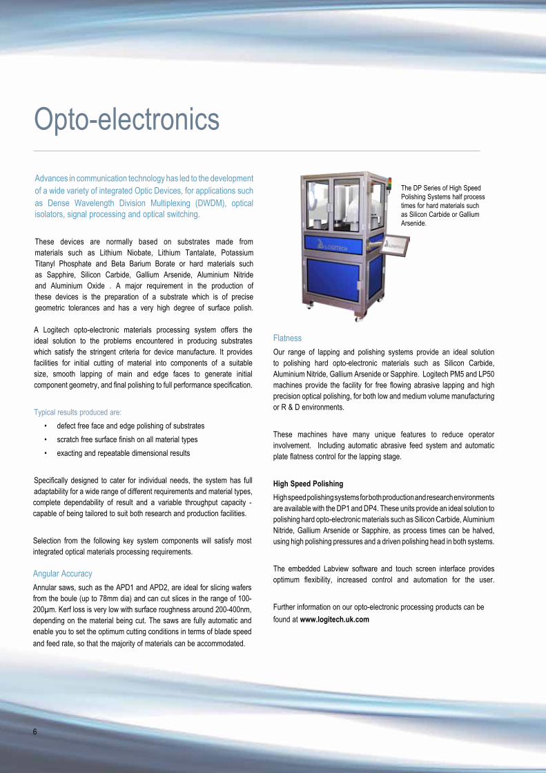
PP5 Jig for fibre array assembly.
APD2 Peripheral Saw with special rotary table dicing an optical sample.
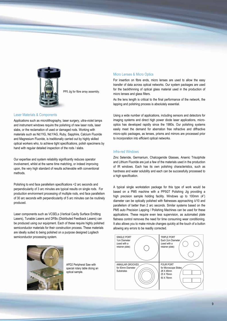
SINGLE PORT1cm Diameter(used with a retainer plate)
TRIPLE PORTEach 2cm Diameter(used with a retainer plate)
ANNULAR GROOVES for 83mm Diameter Substrates
FOUR PORTfor Microscope Slides28 X 48mm25 X 76mm50 X 76mm
10
Geological Sciences
In geological study areas, such as mineralogy, petrography or sedimentology, samples need to be examined microscopically. When carried out using transmitted polarised light there is a requirement for thin sections of known and exact thickness.
Reflected light microscopy is also widely used for applications that require flat and highly polished sample surfaces. The use of electron microscopes also contribute to the need for top quality thin sections of a wide range of materials.
Logitech supplies a comprehensive range of equipment which satisfy all of those needs and allow you to:
• consistently produce the highest quality sections • substantially increase section output • eliminate the need for hand lapping and polishing • easily create sections from differing materials • easily create sections to differing dimensions
If your need is for ultra thin sections of 10 µm thickness or less, thin sections between 20 and 50µm thickness or polished mounts, the following equipment is available.
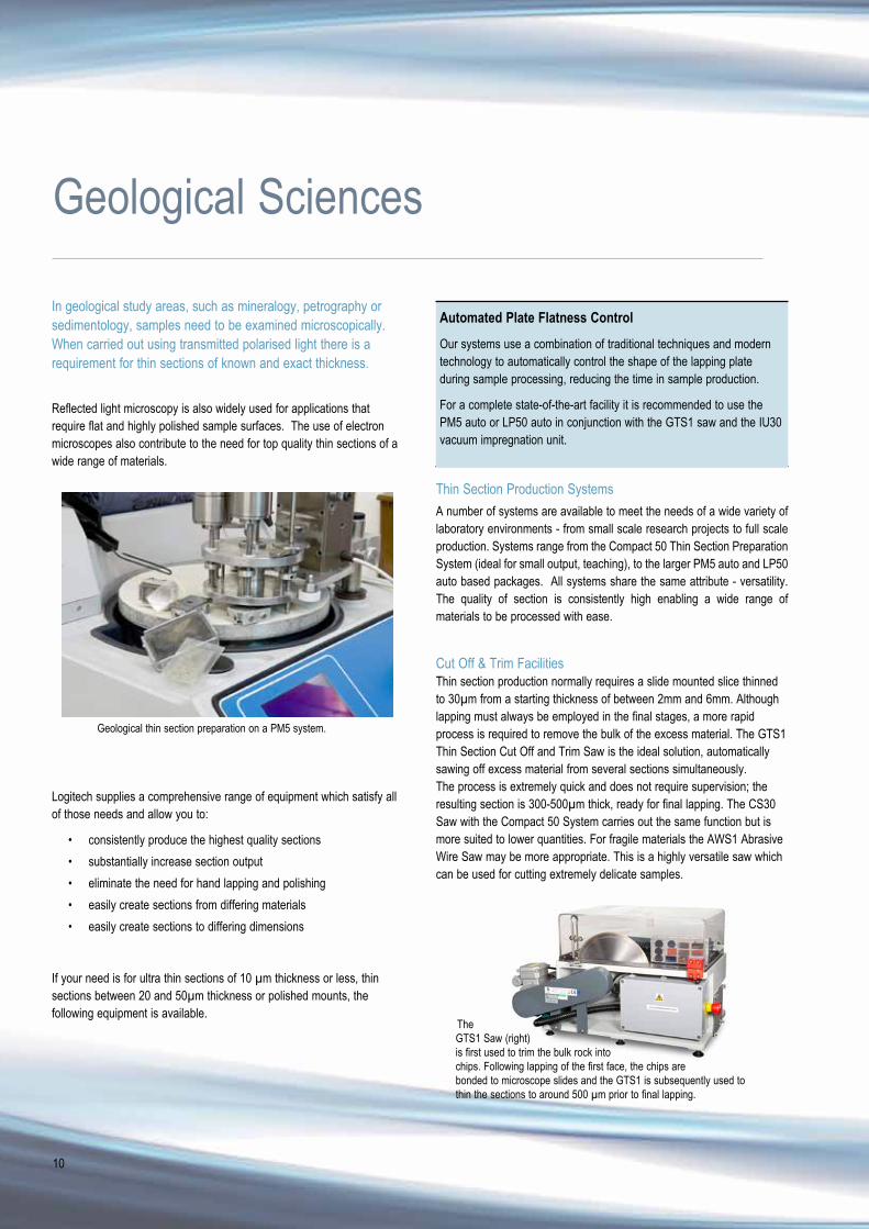
Geological thin section preparation on a PM5 system.
Thin Section Production SystemsA number of systems are available to meet the needs of a wide variety of laboratory environments - from small scale research projects to full scale production. Systems range from the Compact 50 Thin Section Preparation System (ideal for small output, teaching), to the larger PM5 auto and LP50 auto based packages. All systems share the same attribute - versatility. The quality of section is consistently high enabling a wide range of materials to be processed with ease.
Cut Off & Trim Facilities Thin section production normally requires a slide mounted slice thinned to 30µm from a starting thickness of between 2mm and 6mm. Although lapping must always be employed in the final stages, a more rapid process is required to remove the bulk of the excess material. The GTS1 Thin Section Cut Off and Trim Saw is the ideal solution, automatically sawing off excess material from several sections simultaneously. The process is extremely quick and does not require supervision; the resulting section is 300-500µm thick, ready for final lapping. The CS30 Saw with the Compact 50 System carries out the same function but is more suited to lower quantities. For fragile materials the AWS1 Abrasive Wire Saw may be more appropriate. This is a highly versatile saw which can be used for cutting extremely delicate samples.
The GTS1 Saw (right) is first used to trim the bulk rock into chips. Following lapping of the first face, the chips are bonded to microscope slides and the GTS1 is subsequently used to thin the sections to around 500 µm prior to final lapping.
Automated Plate Flatness ControlOur systems use a combination of traditional techniques and modern technology to automatically control the shape of the lapping plate during sample processing, reducing the time in sample production.
For a complete state-of-the-art facility it is recommended to use the PM5 auto or LP50 auto in conjunction with the GTS1 saw and the IU30 vacuum impregnation unit.

11
ImpregnationMany material types are too soft or friable for the production of samples from the raw state. The IU30 Vacuum Impregnation Unit was designed for consolidating these materials by impregnation with synthetic resins prior to sectioning. Utilising a unique double chamber arrangement, which allows both sample and resin to be evacuated separately, the IU30 enables the most difficult of sample types to be impregnated, greatly improving the quality of the finished specimen.
First Face Lapping A standard thin section is 30µm thick uniformity over the rock slice area. To achieve a flat reference surface for subsequent bonding to the slide, one face of the prepared chip is lapped flat in a conditioning ring under a pressure block of 3.5kg load on a grooved, cast iron lapping plate. This can be achieved using a Logietch PM5, LP50 or CL50 Precision Lapping and Polishing System.
Preparing Slides to Uniform Thickness The glass slides for supporting the specimen material must be parallel and of a known thickness. One face of the slide is lapped flat and parallel on either a PLJ2, PLJ7 or CJ30 precision lapping jig, which can be set to stop the lapping action at the required thickness.
Bonding Specimens to Prepared Slides A thin layer of epoxy resin is spread on the dried, lapped face of the chips and the lapped side of the slide is placed on the rock surface. All bubbles need to be eliminated and the slide placed on a bonding jig. This ensures a parallel, effectively zero bond (less than 1µm thick).
The compact 50 thin section preparation system is designed to produce high quality thin sections with a
minimum of capital investment.
The WG2 polishing system - a rapid and economical method for polishing geological samples.
The PLJ7 Large Format Precision Lapping Jig
Lapping Speciments to Final ThicknessThe thinned bonded specimens are now mounted onto a precision lapping jig and lapped to the final desired thickness (typically 30µm). This can be achieved with a Logitech PM5, LP50 or CL50 system.
Polishing (if required)Even the most difficult polishing applications can be satisfied by the WG2 Polishing System, which offers both quality of results and versatility of performance. Capable of producing the highest quality specimens, the WG2 is an ideal complement to a Logitech PM5 based lapping system and is designed to provide the best quality surface finishes, with the fastest possible production rates and the most economical operation. In addition to the production of both polished sections and polished thin section, the WG2 system can be adapted to the polishing of ultra-thin sections by the addition of a small range of operating accessories.
Combined Lapping / Polishing SystemsOccasionally, space, economics or simply low output requirements may preclude the use of separate systems for lapping and polishing, in these circumstances the PM5 or LP50 systems are ideal. Each system will be created to meet your needs, from cutting, lapping and polishing to measurement and testing.The Logitech WG2 polishing head is a versatile product when used with a PM5 system, thus providing the ideal solution for laboratories with a small scale requirement for lapped and polished sections.
Large Format Thin SectionsGeologists, soil scientists and civil engineers increasingly require to prepare sections up to 150 x 100mm (6”x4”). The benefit of large format sections is that the larger surface area can reveal features which would not otherwise be apparent. They are of particular value when analysing soils, concretes or cements. The PLJ7 Large Format Precision Lapping Jig is theideal holding fixture for this application, enabling the production of thin sections up to 150 x 100mm with the highest degree of sample parallelism.

12
Other ApplicationsThe use of Logitech systems is not restricted to the application areas in the preceding pages. These are just a few of the other applications where our systems provide real solutions to complex material preparation problems. When added to the applications already described, it clearly illustrates the high degree of flexibility and wide range of experience we offer in precision materials processing.
Tooth: Thin sections of teeth provide an excellent tool for dental research and can be produced routinely with a Logitech system. Every conceivable requirement can be met, from lapped sections in the 70-100µm range for routine microradio-graphy to polished thin sections of 10-15µm thick for detailed cellular analysis. The techniques employed allow the use of encapsulated material or natural whole teeth and can be adapted to suit a wide range of differing applications.
Bone: Producing high quality thin sections of bone with or without implants, using traditional microtome techniques present major technological problems and generally results in sections of low quality which prevents effective evaluate results.Using a Logitech thin section production system, high quality thin sections to 10µm or less and in formats up to 100mm x 75mm (4” x 3”) can be produced routinely. The methods used are based on Logitech’s proven standard thin sectioning
Metals
Preparation of some types of metal and alloys for ion beam milling and detailed structural analysis requires the production of very thin, 15µm, highly polished and very uniform specimens. Traditional metallurgical polishing techniques do not readily satisfy these requirements and it is these areas of metallographic preparation in which a Logitech system can provide an effective solution.
Thin section of whole tooth, for microradiography purposes.
(Photo courtesy of Oral Biology Group of Glasgow Dental Hospital, Scotland)
Otoliths: In fisheries research, thin sections of otoliths are providing an increasingly useful tool in the analysis of periodic banding patterns for life history studies of fish. Working closely with a major US government department and utilising over 40 years of experience in rock thin sectioning, Logitech has developed a successful method for volume production of otolith thin sections, which offers major advantages to the fisheries research scientist.
Thin section of otolith taken at 200 x magnification. Section is 50µm thick.
(Photo courtesy of Washington State Department of Fisheries, Olympia, USA)
Thin section showing part of a bead in the porous coating of a knee prosthesis. 100 x magnification.
(Photo courtesy of Howmedica, New Jersey, USA)
Polished super alloy section take at 500 x magnification.
Calcified Tissues
13
Polymers Structural defect and stress cracking analysis in polymers and carbon-based materials presents another area where Logitech equipment is successfully used, providing a rapid and reliable method for polishing the ends of carbon fibres and for producing polished thin sections of a wide range of polymers at 30 µm or less in thickness.Thin section of carbon fibre
composite showing fracture after shear loading. Fibre diameter is 7µm.
(Photo courtesy of ICI Advanced Materials, Cleveland, UK)
Others Logitech expertise is not restricted to the areas listed here - there are many interesting problems which have been solved using Logitech equipment and technology and the company is always willing to assist, even in the more unusual applications.
Large format thin section of a petrified tree.
Thin section of pyroelectric ceramic, viewed in transmitted, crossed, polarised light.
(Photo courtesy of GEC Marconi Materials Technology, Caswell, part of Oclaro)
Ceramics Device manufacture using ceramic substrates often involves the production of flat and/or thin layers of delicate and difficult materials such as PZT and lead oxides - another technology sector in which Logitech is a major contributor.
Magnetic Recording Heads Magnetic recording heads are commonly fabricated on 75mm (3”) diameter alumina/titanium composite wafers. Usually, there is a requirement to remove a few mm from the final evaporated coating which itself may be only 5 µm thick and a number of manufacturers use Logitech equipment for this stringent application.Magnetic Recording Head.
Concrete Thin sections of concrete are prepared for a number of different tests, such as porosity determination, inclusion analysis and mineral composition. The combination of soft cement matrix and hard aggregate is difficult to work with; many of the cement phases are water sensitive, preventing the use of aqueous abrasive carrier fluids; thin sections must be produced with a thickness of 20µm thickness, if fine grained cement is to be studied.
Thin section of concrete
LEDs High brightness LEDs (HB LEDs) use materials such as GaN, SiC and Sapphire. Logitech has experience in processing the materials from R&D up to a medium volume manufacturing throughout. Typical target surface roughness values are <3nm, with optimised surface roughness values of <1nm for materials such as sapphire.
High brightness LED.

14
Test & MeasurementLogitech optical test and measurement equipment is used worldwide for inspection of finished components and correct preparation of sample assemblies prior to polishing.
Thickness MeasurementAccurate measurement of specimen thickness is catered for either by contact or non-contact electronic gauges. Both instruments provide measurement precision of +/-0.0001mm (0.00001”) with excellent repeatability and linearity. The NCG-2, Non-Contact Gauge is used where surface contact can cause damage to the specimen, while the contact gauge provides a robust and accurate general purpose thickness measurement capability. Our CG10 gauge has the added benefit of Microsoft Excel compatability and provides results direct to your PC.
CG10 Precision Electronic Measurement System delivers highly accurate results over a
wide measuring range.
Flatness MeasurementQuick and accurate measurement of component flatness during processing and on completion is provided by the GI20 Flatness Measurement System. This grazing incidence interferometer is suitable for use with non-reflective surfaces up to a surface roughness Ra of 300nm. The tool can measure surface flatness of material with a surface roughness requirement of <300nm, up to 6” (150mm) in diameter. The unit measures 2 µm per fringe with excellent clarity. The system is compatible with PP5 and PP6 Polishing Jigs.
The LI10 Interferometer is a multiple beam Fizeau Interferometers suitable for measuring polished specimens up to 100mm (4”) and 150mm (6”) diameters respectively. This unit offer a rapid and accurate method for the optical measurement of polished surface flatness, with a reference flatness of λ/10.
NCG-2 Non Contact Guage offers a compact, yet highly
sensitive solution for precision measurement of fragile, soft or
highly polished materials.
The GI Flatness Measurement System, allows the flatness of ground, lapped and semi-polished surfaces to be accurately accessed.
“In-process” measurements can be made without having to demount the sample from the lapping / polishing jig.
Angular Measurement & SettingThe LG2 Autocollimator is ideal for use in applications where high levels of parallelism are required, such as in laser rod polishing. Using the LG2, component faces can be accurately aligned with the polishing plane to achieve end face parallelism accuracy down to 2 arc seconds. Alternatively, the LG2 can be used to set the polishing surface at a precise predetermined angle, thus greatly improving the precision with which wedge angles can be produced.
Further information on our test and measurements products can be found at www.logitech.uk.com
Fully compatible with the PP5 Precision Polishing Jig, the LG2 autocollimator provides a high accuracy facility for parallel or angular specimen adjustment.

15
Accessories
Jig Outside Diameter
Total Thickness Variation
Range of Jig loads applied
Angular adjustment range
PP5 83mm +/- 1.5 µm 0.2 - 2.8kg +/-1.5 °
PP6 112mm +/- 2 µm 0.2 - 4.8kg +/-1.5 °
PP8 160mm +/- 3 µm 0.2 - 6.7kg +/-1.5 °
PP9 210mm +/- 4 µm 0.2 - 9.5kg NA
Pads & Cloths
The Logitech range of polishing pads and cloths provide a comprehensive selection of materials for fine surface polishing of a wide range of sample types. Pads & cloths are chosen because of texture, and capability to retain abrasive on the pad or cloth surface, in an efficient and economic manner. This ensures that samples are produced to the highest quality of surface finish whilst obtaining the best possible surface flatness.
Jigs
Our wide range of precision jigs, hold a diverse range of sample sizes and material types during lapping and/or polishing.
All our jigs are precision made and hand finished to ensure the highest accuracy levels. The easy to read LCD display gauge provides results within 1µm of accuracy. The digital gauge informs the operator when the required removal rate has been reached.
Pads & Cloths Chemcloth Polishing ClothsLogitech Chemcloth Polishing Cloths are designed to satisfy the exacting requirements of Chemical Mechanical Polishing (CMP). The black napped urethane surface layer is intrinsic to the substrate giving superior nap strength and longer pad life.
Chemcloth is ideally suited to a variety of polishing processes including:• Production due to of the cloth’s superior wear resistance. • Finishing under corrosive acid and alkaline conditions • High speed polishing operations due to superior nap strength.
PadsEP1 The EP1 has a foamed elastomer structure with controlled cells. Its unique structure and high hardness improves planarity and is designed for optimum polishing of Silicon, Sapphire and optical materials.
EP2 The EP2 has a micro-cellular structure that enables it to act in a “sponge-like” manner while maintaining the hardness and flatness. It is designed for optimum polishing of Silicon, Sapphire and optical materials. Excellent flatness and fast polishing rates.
EP3 Similar to the EP2 but has a slightly lower hardness rating. It is designed for optimum polishing of soft metal materials. It too has excellent flatness and fast polishing rates.
SB4 SB4 pads feature an open pore structure and a less aggressive urethane composition than other pads. They are ideal for low to medium pressure applications with fragile crystals or delicate surfaces. Often used as a base pad in conjunction with our IC1K pads.
SB10 SB10 is a denser, harder pad with a smaller pore structure than our SB4 pad. It is often used for polishing glass, quartz or ceramics with consistent, reproducible results.
IC1K The IC1K pad is made of rigid, microporous polyurethane. This allows it to planarize across wide gaps, providing excellent removal rates and localised uniformity. The small pore structure works with slurries to minimize scratching and provide optimum polishing performance.
The Logitech range of precision jigs and accessories.

16
Consumable Products To complement the range of cutting, lapping and polishing equipment, we supply a variety of consumable products to aid you in the production of top quality samples.
Products are chosen on the basis of the quality of results produced and on their suitability for the many precision materials processing applications our systems are used. Each product has been tested and approved by our experts.
A summary of the products available is given here; further details on the full range of Logitech Consumable products are available at www.logitech.uk.com.
Logitech supplies a range of consumable products required for precision material processing. Including
lubricants for precision lapping & polishing jigs, soluble oils, vacuum oils, saw blades and wires.
Abrasive PowdersSilicon Carbide PowdersSupplied in a wide range of grit sizes, these high quality abrasive powders can be used where repeatability of material removal rate is required. Typical applications include:
• Thin Rock Section Production • Silicon Wafer Back Thinning • Hard Materials Back Thinning • Ferrite Component Processing • Calcified Tissue Thin Section Production
Calcined Aluminium Oxide PowdersCalcined Aluminium Oxide Powders are suitable for a very wide range of precision lapping and polishing operations and offer many advantages. These include:
• Reduced process times • Improved surface finish • Lapping pressure and plate speed increases • Improvements in normal process times leading to greater production output • Higher quality surfaces
Ultra-fine Aluminium Oxide PowdersSub-micron Aluminium Oxide Powders for polishing operations in critical surface preparation. They give excellent results when used for polishing:
• Optical Components • Ceramics • Ferrite Components • Electro-Optic Materials • Plastics • Semiconductor Materials
Boron CarbideBoron Carbide is a very hard abrasive, filling the need for an abrasive powder which is harder than silicon carbide but less expensive to use than diamond.Applications for the use of boron carbide include the processing of ceramic materials, very hard optical materials such as sapphire,
Polishing Suspensions
SF1SF1 Polishing Fluid (Alkaline colloidal silica) is suitable for polishing silicon wafers and a wide range of optical/opto-electronic components.
ChemloxA sodium hypochlorite-based polishing fluid, suitable for CMP (chemo-mechanical polishing) of gallium arsenide and similar semiconductor materials on the appropriate Logitech polishing equipment.

17
Resins
Epoxypack 301
A two part epoxy resin with a Refractive Index of 1.54. Suitable for a wide range of mounting and impregnation applications, including bonding thick rock sections to microscope slides and the impregnation of porous and friable samples prior to further processing.
UV Resin
A urethane acrylic resin which cures under ultraviolet light, used for temporary, controlled thickness bonding applications.
Mounting Resins
Resins for mounting samples in Logitech Annular Saws are also available.
Further information on the Logitech mounting media and consumables range can be found at www.logitech.uk.com
Waxes
High Melting Point Thin Film Bonding Wax.
Melting Point Range: 157-162°C.Suitable for semiconductor wafer bonding for high temperature processing.
Plasticised General Bonding Wax
Melting Point Range: 57-59°C. Suitable for a wide range of temporary bonding applications.
Quartz Wax
Melting Point Range: 66-69°C Particularly suited to the bonding/mounting of electro-optic and optical materials.
Glycol Phthalate
Melting Point Range: 71-122°C For bonding semiconductor wafers where high shear strength is required.
Thin Bonding Wax
Melting Point Range: 50-55°C
Ideal for holding substrates in place during slicing, dicing, polishing and lapping.
Wax Cement
Melting Point Range: 110-120°C.
Used for bonding in ceramics and semiconductor applications.
Mounting Media Microscope Slides, Coverslips & Substrates
Logitech Microscope Slides are manufactured to stringent production quality control procedures, and benefit the user with ground edges for greater safety and ease of handling.The slides are available in a variety of sizes, ranging from “standard” sizes such as 28 x 48mm to large format slides of 150 x 100mm.
Logitech Microscope Slide Cover Slips are also available in a range of sizes. Optical qualities, such as flatness, planarity, homogeneity, refractive index and dispersive power all meet the most exacting industry standards. The slides conform to the standard microscope cover slip thickness of 0.170mm.
Logitech Glass Support Substrates are manufactured from float glass, and can be supplied in a range of diameters to accept different sizes of wafer sample. All substrates are 6mm thick, and the maximum parallelism error for lapped substrates is 2µm.
Other Products
Diamond Powders & Suspensions DP diamond powders are available in a number of µm sizes and types, for applications ranging from thin section polishing to the lapping of sapphire.
Ethane Diol and Ethane Diol PlusIdeal for use in the lapping and polishing of water-soluble materials, ethane diol is an effective carrier with many powders including diamond, silicon carbide and aluminium oxide.
Ecoclear A non-solvent, non-toxic cleaning fluid designed for wafer demounting and the removal of wax, pitch and solvent-soluble resists from optical and electronic components of glass, ceramic, metal, etc.

18
Technology Transfer A key part of the Logitech “package” is in Technology Transfer. Many years of experience in materials processing and equipment supply have clearly indicated that instruction manuals are seldom enough to ensure you achieve the best results.
We provide comprehensive operator training with each machine system. This usually takes the form of a full three day course which would typically comprise:
• a presentation of the equipment and its features• a demonstration by our expert team on how to use the system to prepare your samples• process trials and practical sample preparation by the trainee, with appropriate guidance and supervision• examination of daily maintenance routines and training in troubleshooting• further discussion and guidance on associated topics and requirements.
Courses are limited to three individuals with similar training needs, allowing very close, and often one to one tuition. As our courses are tailored to meet your needs, all key requirements and problems will receive full attention. Emphasis is placed on processing your own samples, ensuring training is always relevant and practical.
Upon completion of this intensive training course, you will be fully equipped to prepare your samples and to effectively manage minor processing or equipment problems. Ensuring a successful installation in your laboratory.
Re-trainingOver time, changes occur which make re-training a necessary and cost-effective investment. This may be to ensure new members of your lab team become fully competent on your Logitech system, rather than receiving second hand instruction, or because the materials and processing you wish to carry outhas changed.
In such a case, a Logitech training course can be purchased to enhance your overall materials processing capability.
One of Logitech’s fully equipped applications and development laboratories, used for continuous process development and a wide range of customer training programmes.

19
Logitech’s continued commitment to customer support is demonstrated by the high volume of satisfied clients in; universities, colleges, research establishments and government agencies covering a diverse range of global industrial enterprises. We are proud of our prestigious client base which includes many of the world’s leading academic centres and industrial organisations.
All Logitech customers benefit from the combination of service and facilities described below.
After Sale SupportFull support is provided by our Customer Services team, whose primary function is to provide a comprehensive advisory service and ensure that the system produces results at your premises. Should problems arise with the equipment, or its use, Logitech always strive to provide solutions in the quickest possible manner. A “no quibble” repair and replacement policy is in operation and highly regarded by our clients.
Every Logitech system is supplied with a twelve month warranty, providing replacement parts and repairs free of charge during this time.
Further support is provided through technology transfer and regular equipment updates and processing methods. The Logitech team of specialists are always available to provide assistance, guidance and advice.
It is our intention to develop a close and continued relationship with our customers. A full range of consumables, replacement parts and re-training are offered to assist in achieving this aim.
Continuous ImprovementWe continue to invest in our products, services and staff to enable us to evolve with our client and market needs, through the development of new or improved products and processes.
Much of this effort is focused on providing improvements to existing technologies, thus ensuring you are provided with the most up to date solution.
The preparation of samples, both standard and special, is also under the control of the development department to ensure new processes are proven in the laboratory before being released to our clients.
Due to our level of in-house skills and laboratory facilities, one of our material processing experts will work with you to develop the best process. Our expert will also provide you and/or your team with system and process training - ensuring you obtain maximum results from our products.
Customer Support

Logitech Limited
Erskine Ferry Road,Old Kilpatrick, GlasgowG60 5EU Scotland
T: +44 (0) 1389 875444F: +44 (0) 1389 890956E: [email protected]: www.logitech.uk.com