Precision glass molding of freeform optics
11
Updated 3/20/14 Precision glass molding of freeform optics Dustin Gurganus* a , Joseph D. Owen a , Brian S. Dutterer a , Spencer Novak b , Alan Symmons b , Matthew A. Davies a a Dept. of Mech. Eng. and Eng. Science, UNC Charlotte, 2201 University City Blvd., Charlotte, NC, USA 28223; b LightPath Technologies, 2603 Challenger Tech. Court, Orlando, FL USA, 32826 ABSTRACT Precision glass molding is a viable process for the cost-effective volume production of freeform optics. Process development is complex, requiring iterative trials of mold manufacture and metrology, glass mold prototyping, metrology and functional testing. This paper describes the first iteration in the development of a process for an Alvarez lens for visible light. The challenges of this optic are extremely tight band-RMS tolerances on a freeform shape over a maximum clear aperture of 45 mm, a 16:1 aspect ratio and a freeform departure of 329 micrometers. A freeform glass mold for an Alvarez lens was manufactured by coordinated-axis diamond turning in a mold substrate using a custom tool error correction method. The results of prototype precision glass molding are also reported. Mold surfaces and molded optical surfaces are analyzed with scanning white light interferometry. A surface roughness of approximately 3 nm RMS is obtained for both the mold substrate and the glass optic with high-fidelity reproduction of micro-surface structure in the glass. These measurements also identify challenging areas, particularly the presence of mid-spatial frequency errors on the optic originating from the machine thermal control system. The form of the molds was also measured with a profilometer; however, the mold surface does not agree with the expected prescription with an overall deviation in form of approximately 10 μm. The machining process is expected to have sub-micrometer error and the sources of this discrepancy are still being determined. Metrology of the glass optics is currently in progress. Keywords: Precision glass molding, freeform optics, diamond turning, freeform metrology. 1. INTRODUCTION Freeform optics are a potentially disruptive technology in the optics industry 1 . However, to become pervasive, production costs must be made competitive. For infrared optics, direct ultraprecision machining is viable process chains 2,3 particularly in non-moldable materials such as germanium 4 . For volume production of optics for use in the visible spectrum, direct machining methods are cost prohibitive. Additionally, glass transmissive freeform optics designed to operate in the visible wavelength range have demanding tolerances in terms of form, finish and mid-spatial frequencies. Since direct machining of optical glass requires grinding and post polishing, meeting these tolerances is often extremely costly. Precision glass molding has become a leading process for producing optics in large quantities both in visible and IR transparent glasses 5– 7 . Precision glass molding has seen decades of development from the early work of Webb that led to a patented machine 8 with a described process. Webb’s patent covered multiple configurations of molding. In this design, a full glass molding cycle was implemented and controlled. Starting from an initial glass blank that could be a disk or rod, the mold cavity was first back-filled with hydrogen, helium or nitrogen, and the mold tooling was brought together at high-pressure with a controlled temperature in the range of 500°C to 600°C. Su, et al. continued the development of the process, simulating the flow patterns in glass molding and connecting these to index variations. 9 Yi et al. extending this work to applications in aspherical optics. 10 Cogburn et al. improved the process speed and cost for industrial applications. 11 This research has translated into processes employed in industry. 12 Most industrial applications are for axisymmetric optics limited in diameter to approximately 25 mm. Larger optical molds take more time to heat and cool which adds to cycle times. To our knowledge, this is the first research to address inherent issues of the glass molding of large freeform optics with no axis of rotational symmetry either on or off the optic, adopting the definition of freeform optics provided by Fang et al. 13 This work targets precision glass molding of freeform Alvarez lenses 14 with a number of challenging specifications: (1) diameters exceeding 40 mm; (2) an aspect ratio of 16:1; (3) band- RMS tolerances less than 100 nm (see Section 3.1). This requires high forces and temperatures to produce large deformations in the glass molding process, and the freeform shape of the mold can lead to complex glass flow patterns.
Transcript of Precision glass molding of freeform optics

Updated 3/20/14
Precision glass molding of freeform optics Dustin Gurganus*a, Joseph D. Owen a, Brian S. Dutterer a, Spencer Novakb, Alan Symmons b,
Matthew A. Davies a
aDept. of Mech. Eng. and Eng. Science, UNC Charlotte, 2201 University City Blvd., Charlotte, NC,
USA 28223; bLightPath Technologies, 2603 Challenger Tech. Court, Orlando, FL USA, 32826
ABSTRACT
Precision glass molding is a viable process for the cost-effective volume production of freeform optics. Process
development is complex, requiring iterative trials of mold manufacture and metrology, glass mold prototyping, metrology
and functional testing. This paper describes the first iteration in the development of a process for an Alvarez lens for
visible light. The challenges of this optic are extremely tight band-RMS tolerances on a freeform shape over a maximum
clear aperture of 45 mm, a 16:1 aspect ratio and a freeform departure of 329 micrometers. A freeform glass mold for an
Alvarez lens was manufactured by coordinated-axis diamond turning in a mold substrate using a custom tool error
correction method. The results of prototype precision glass molding are also reported. Mold surfaces and molded optical
surfaces are analyzed with scanning white light interferometry. A surface roughness of approximately 3 nm RMS is
obtained for both the mold substrate and the glass optic with high-fidelity reproduction of micro-surface structure in the
glass. These measurements also identify challenging areas, particularly the presence of mid-spatial frequency errors on
the optic originating from the machine thermal control system. The form of the molds was also measured with a
profilometer; however, the mold surface does not agree with the expected prescription with an overall deviation in form
of approximately 10 μm. The machining process is expected to have sub-micrometer error and the sources of this
discrepancy are still being determined. Metrology of the glass optics is currently in progress.
Keywords: Precision glass molding, freeform optics, diamond turning, freeform metrology.
1. INTRODUCTION
Freeform optics are a potentially disruptive technology in the optics industry 1. However, to become pervasive, production
costs must be made competitive. For infrared optics, direct ultraprecision machining is viable process chains 2,3 particularly
in non-moldable materials such as germanium 4. For volume production of optics for use in the visible spectrum, direct
machining methods are cost prohibitive. Additionally, glass transmissive freeform optics designed to operate in the visible
wavelength range have demanding tolerances in terms of form, finish and mid-spatial frequencies. Since direct machining
of optical glass requires grinding and post polishing, meeting these tolerances is often extremely costly. Precision glass
molding has become a leading process for producing optics in large quantities both in visible and IR transparent glasses5–
7. Precision glass molding has seen decades of development from the early work of Webb that led to a patented machine8
with a described process. Webb’s patent covered multiple configurations of molding. In this design, a full glass molding
cycle was implemented and controlled. Starting from an initial glass blank that could be a disk or rod, the mold cavity
was first back-filled with hydrogen, helium or nitrogen, and the mold tooling was brought together at high-pressure with
a controlled temperature in the range of 500°C to 600°C. Su, et al. continued the development of the process, simulating
the flow patterns in glass molding and connecting these to index variations.9 Yi et al. extending this work to applications
in aspherical optics.10 Cogburn et al. improved the process speed and cost for industrial applications.11 This research has
translated into processes employed in industry.12
Most industrial applications are for axisymmetric optics limited in diameter to approximately 25 mm. Larger optical molds
take more time to heat and cool which adds to cycle times. To our knowledge, this is the first research to address inherent
issues of the glass molding of large freeform optics with no axis of rotational symmetry either on or off the optic, adopting
the definition of freeform optics provided by Fang et al. 13 This work targets precision glass molding of freeform Alvarez
lenses 14 with a number of challenging specifications: (1) diameters exceeding 40 mm; (2) an aspect ratio of 16:1; (3) band-
RMS tolerances less than 100 nm (see Section 3.1). This requires high forces and temperatures to produce large
deformations in the glass molding process, and the freeform shape of the mold can lead to complex glass flow patterns.

Development of the precision glass molding process requires a multi-stage iterative process as shown in Figure 1. The
first step is to define the freeform geometry and develop a manufacturing process for freeform molds. The next step is to
perform metrology on the molds to verify the geometry and to ensure that the tolerances exceed the requirements of the
final optics. The precision glass molding process is then designed and tested including the form, form repeatability,
mechanical integrity, and cosmetic quality of test optics. The test optics are manufactured, measured and compared against
the measured mold geometry and corrections are generated. The process then repeats with the production of a corrected
mold geometry and corrected optics. This paper describes mold manufacturing, metrology and molding tests for the first
iteration of this multi-stage molding process.
Figure 1. Schematic of the iterative design process.
2. OPTICAL PRESCRIPTION AND TOLERANCES
The goal of this research is to mold a freeform Alvarez lens with tolerances necessary to perform in the visible light
spectrum. The classical Alvarez lens combines two optics with cubic polynomial surfaces (Figure 2(a)). When the optics
are aligned, they have zero optical power. However, when a relative shear, d, is introduced between the optics, the
composite structure is equivalent to a plano-spherical lens with optical power that depends on the shear (Figure 2(b)).
Figure 2: (a) Alvarez lens components and (b) composite surface where curvature and hence focal length depends on d.
The performance specifications of the application require tight manufacturing tolerances. These tolerances (Table 1) were
specified as band-RMS tolerances for defining the errors bounds as a function of spatial wavelength for different optical
diameters. The optical prescription is of the form given in Equation (1),

2 2
22
2 2
1 2 3 4 5
3 2 2 3
6 7 8 9
4 3 2 2 3 4
10 11 12 13 14
( , )
1 1 1 1
x y
x x y y
r x r yz x y
K r x K r y
C x C y C x C xy C y
C x C x y C xy C y
C x C x y C x y C xy C y
(1)
where xr and yr are the radii of curvature, xK and yK are conic constants, and iC are constants defining the polynomial
form. The maximum clear aperture was 45 mm and total sag of the freeform surface was 329 µm. A plot of the surface
is shown in Figure 3.
Figure 3: Plot of the Alvarez lens surface with clear aperture 45 mm and total sag of 329 µm.
3. MANUFACTURING PROCESS
3.1 Description of Molding Equipment and Mold Tooling Design
As shown if Figure 4, precision glass molding (PGM) involves the heating of a glass preform above its glass transition
temperature, compression molding into a desired shape. The viscosity-temperature relationship of the glass is exploited to
achieve the desired flow and final properties of the molded optic. While many variations of PGM exist, a schematic
representation of the process is shown in Figure 4 where a single lens is molded and the volume of the preform must be
tightly controlled.
Table 1: Required band-RMS tolerances.
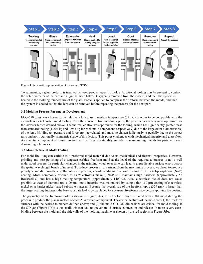
Figure 4: Schematic representation of the steps of PGM.
To summarize, a glass preform is inserted between product-specific molds. Additional tooling may be present to control
the outer diameter of the part and align the mold halves. Oxygen is removed from the system, and then the system is
heated to the molding temperature of the glass. Force is applied to compress the preform between the molds, and then
the system is cooled so that the lens can be removed before repeating the process for the next part.
3.2 Molding Process Parameter Development
ECO-550 glass was chosen for its relatively low glass transition temperature (371°C) in order to be compatible with the
electroless nickel coated mold tooling. Over the course of trial molding cycles, the process parameters were optimized for
the Alvarez lenses defined above. The thermal control was optimized for the tooling, which has significantly greater mass
than standard tooling (1.204 kg and 0.965 kg for each mold component, respectively) due to the large outer diameter (OD)
of the lens. Molding temperature and force are interrelated, and must be chosen judiciously, especially due to the aspect
ratio and non-rotationally symmetric shape of this design. This poses challenges with mechanical integrity and glass flow.
An essential component of future research will be form repeatability, in order to maintain high yields for parts with such
demanding tolerances.
3.3 Manufacture of Mold Tooling
For mold life, tungsten carbide is a preferred mold material due to its mechanical and thermal properties. However,
grinding and post-polishing of a tungsten carbide freeform mold at the level of the required tolerances is not a well
understood process. In particular, changes in the grinding wheel over time can lead to unpredictable surface errors across
the spatial wavelength bands of interest. To reduce process errors arising from the machining process, we chose to produce
prototype molds through a well-controlled process, coordinated-axis diamond turning of a nickel-phosphorus (Ni-P)
coating. More commonly referred to as “electroless nickel”, Ni-P still maintains high hardness (approximately 55
Rockwell-C) and has a high melting temperature (approximately 1400°C). Also, electroless nickel does not cause
prohibitive wear of diamond tools. Overall mold integrity was maintained by using a thin 150 µm coating of electroless
nickel on a harder nickel-based substrate material. Because the overall sag of the freeform optic (329 µm) is larger than
the target coating thickness, the base substrate had to be machined to a near-net freeform shape before applying the coating.
The geometry of the freeform mold is shown in Figure 5(a). This freeform mold is paired with a flat mold during the
process to produce the planar surface of each Alvarez lens component. The critical features of the mold are: (1) the freeform
surfaces with the desired tolerances defined above; and (2) the mold OD. OD dimensions are critical for mold tooling. If
the OD gap (Figure 5(b)) is too small, this can lead to uneven mold surface connection and release. In more severe cases
binding between the mold and the sidewalls of the molding machine as shown by the red regions in Figure 5(b).
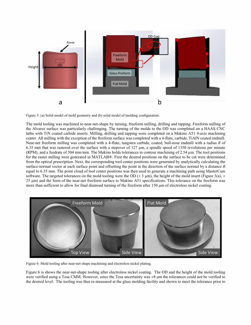
Figure 5: (a) Solid model of mold geometry and (b) solid model of molding configuration.
The mold tooling was machined to near-net-shape by turning, freeform milling, drilling and tapping. Freeform milling of
the Alvarez surface was particularly challenging. The turning of the molds to the OD was completed on a HAAS CNC
lathe with TiN coated carbide inserts. Milling, drilling and tapping were completed on a Makino A51 4-axis machining
center. All milling with the exception of the freeform surface was completed with a 4-flute, carbide, TiAlN coated endmill.
Near-net freeform milling was completed with a 4-flute, tungsten carbide, coated, bull-nose endmill with a radius R of
6.35 mm that was rastered over the surface with a stepover of 127 μm, a spindle speed of 1350 revolutions per minute
(RPM), and a feedrate of 304 mm/min. The Makino holds tolerances in contour machining of 2.54 µm. The tool positions
for the raster milling were generated in MATLAB®. First the desired positions on the surface to be cut were determined
from the optical prescription. Next, the corresponding tool center positions were generated by analytically calculating the
surface-normal vector at each surface point and offsetting the point in the direction of the surface normal by a distance R
equal to 6.35 mm. The point cloud of tool center positions was then used to generate a machining path using MasterCam
software. The targeted tolerances on the mold tooling were the OD (± 3 μm), the height of the mold insert (Figure 3(a), ±
25 μm) and the form of the near-net freeform surface to Makino A51 specifications. This tolerance on the freeform was
more than sufficient to allow for final diamond turning of the freeform after 150 μm of electroless nickel coating.
Figure 6: Mold tooling after near-net-shape machining and electroless nickel plating.
Figure 6 is shows the near-net-shape tooling after electroless nickel coating. The OD and the height of the mold tooling
were verified using a Tesa CMM. However, since the Tesa uncertainty was ±8 μm the tolerances could not be verified to
the desired level. The tooling was thus re-measured at the glass molding facility and shown to meet the tolerance prior to

electroless nickel coating. Because of the tight OD tolerance, the final OD was turned at the glass molding facility to fit
the with the molding machine.
3.4 Mold surface manufacturing
After electroless nickel coating, the final mold surface was generated on a Moore Nanotechnology 350 FG. Critical parts
of this process were the method of machining the freeform, thermal effects during machining, and tool path generation.
Since a freeform surface requires at least three degrees of freedom to generate, two machining methods were possible: (1)
diamond raster milling (x-y-z) and (2) coordinated-axis (x-z-C) diamond turning. In milling, a rotating single-flute diamond
tool is rastered over the surface using three linear degrees of freedom x, y, and z. In coordinated-axis diamond turning (so-
called slow tool servo or STS machining), the workpiece rotates and is cut with a slow-moving diamond tool utilizing two
linear degrees-of-freedom, x and z, and one rotational degree-of-freedom, C. For surfaces that have low slopes such as this
one, STS has many advantages including time to machine, surface finish and form accuracy. Thus, STS was chosen to
generate the freeform mold surface. The final surface of the mold includes both the freeform prescription and the blends
at the edges. The blends prevent sharp edges where the freeform prescription ends. Such edges can cause unmachinable
features, interruptions in the flow patterns of the glass, stress concentrations and catalyze defects in the final optics. Taking
a slice through the freeform provides a 2D schematic (Figure 7) of the surface profile. The edge of the freeform aperture
creates a convex upward trending curve. Using the angle θ between the edge of the prescription and the horizontal, an
initial concave curve is calculated to bring the freeform edge upwards. Since the blend needs to bring the edge up to the
flat of the mold, there is a concave curve generated at the edge. Calculating the points where the two curves end, allows
the generation of a line segment to complete the blend. The method produces an analytical description of the freeform
surface and the blend radii from which a toolpath can be generated for STS machining.
Figure 7: 2D profile view of blend construction.
In prior research, a procedure for creating a freeform toolpath while correcting inherent tool errors was established.15,16
The major errors in STS machining of an optic on this scale (~ 40 mm) originate from the diamond tool. They are tool
radius error; tool waviness and tool decenter. The process of generating the tool path proceeds as follows. First, points
along the surface where the tool will cut are selected based on the desired surface finish and form of the final optic: greater
spacing of points along the tool path lead to form errors while the spacing between subsequent paths determines the
theoretically attainable surface finish. Second, MATLAB® is used to generate the surface normal vector at each point
using the analytical description of the surface. The nominal tool position is then generated by a vector offset of the surface
point in the direction of the normal vector and having magnitude equal to the tool radius. Next, the errors of the tool must
be measured and compensated in the tool path generation. Error identification is completed by cutting a concave test sphere
and measuring the profile with profilometry. From this data, the radius error in the tool, its waviness and tool decenter can
be calculated and compensated in the machine path generation.
The final surface was machined with a 0.25 mm (nominal) radius diamond tool and a feed per spindle revolution of 4 µm.
The spindle speed is not fixed during coordinated-axis machining to allow for synchronization of z stroke and C rotation,
but it remained below 100 RPM throughout the operation. To minimize thermal errors, the machine was allowed to come

to thermal equilibrium in the temperature-controlled laboratory for 8 hours before starting the machining operation which
had a duration of 5 hours.
4. FREEFORM METROLOGY OF MOLD
To close the loop on the manufacturing process, the mold geometry was compared to the molded optics and both are
corrected to compensate for machining errors and errors in the glass molding process. Form metrology on the mold was
completed on a Mahr MahrSurf LD260 profilometry machine. Measurements were completed in two operations with a
probe radius of 0.5 mm. In the first operation, 60-line scans were taken along the surface with a data point spacing of 1
μm in the scan direction and a grid stepover between scans of 1 mm. Ball center position was reported for each contact
point. This set of scan lines took approximately one hour. Before the second operation, the mold tooling was rotated 90
degrees and 5 additional tie scan lines were taken with a data point spacing of 1 µm, and a grid stepover of 10 mm. These
tie line scans are taken at the end of long surface scans to compensate for thermal drift. When the profilometer is running,
heat sources such as motors etc. cause changes in the dimensions of the system and thus measurement errors. By the end
of an hour, the machine has reached thermal equilibrium, and therefore the tie lines will be stable representations of the
surface profiles taken.
Utilizing MATLAB®, the metrology data was compared to the ideal machined surface generated from the optical
prescription. The comparison procedure was completed as shown in Figure 8. The same mathematical approach described
in Section 3 as was used to generate ideal center locations for the spherical probe from the optical prescription. The probe-
center location was generated by offsetting each surface point by the probe radius in the direction of the local surface
normal. After the offset, the grid of probe center locations did not match the grid spacing of the line scans, Thus, the data
was interpolated (using functions “scatteredInterpolant”) to the regular grid points. The two data sets were then compared.
Because of uncertainties in the rigid body positions of the mold on the profilometer, small rigid body translations (x, y,
and z) and rotations (about x, y, and z) are introduced to the data to minimize the difference between the data and the ideal
probe-center positions.
Figure 8: The data profiles are compared to one another through translation in x, y, and z and rotation around the x, y, and z axes.
The current estimates of the uncertainties in surface form are approximately 5 μm P-V and the profile of the errors is
shown in Figure 9. These errors are larger than expected from the STS turning operation based on previous experience.
Thus, we are continuing to analyze sources of error in our machining set-up, the metrology arrangement and the data
processing to identify the cause of discrepancies. For example, the analysis does not account for all errors which can occur
in profilometry. Additional and more involved morphological filtering will be required to eliminate this error from the
measurements. One method of reduction of this error is the use of multiple angles of data collection. However, the freeform
surface could still introduce errors from probe tip offsets due to varying surface forces caused by the changing slope of
the freeform. These errors will be further quantified by measuring a spherical artifact by the same method and comparing
to other metrology techniques.

Figure 9: Measured surface errors
For glass molding, a common assumption is that the molded optic will replicate the mold surface features at scales well
below one micrometer. Therefore, surface roughness and mid-spatial frequencies will be replicated on the glass surface.
The theoretical surface finish determined by considering a slice of the turned surface perpendicular to the cutting direction
will be dominated by circular cusps generated by the diamond tool. It can be calculated from Equation 2,
2
24
fRa
R (2)
where f is the feed of the tool per revolution and R is the tool radius. Based on the machining parameters given above,
the theoretical best surface finish is 2.7 nm.
Figure 10: Surface finish of the freeform mold and image of diamond turned freeform mold tooling.
The target surface finish for the final optics was 2 nm RMS measured using a 40x objective and processed with an 80 μm
high pass filter. Using a Zygo NexView scanning white light interferometer (SWLI), the freeform mold tooling surface
was evaluated by taking five independent measurements across the surface. Average surface roughness of 2.1 nm Ra and
2.5 nm RMS were found. Figure 10 shows an example surface measurement and an image of the diamond turned mold
surface. The cusp pattern generated by the tool cutting right to left in each pass with a stepover of 4 μm is evident in the
SWLI image in Figure 10 and this dominated the surface finish. However, other patterns along the cutting direction are
evident likely arising from slight tool vibration and tool-material interaction. Measuring larger sections of the surface as
shown in Figure 11 show mid-spatial frequencies generated by oscillations in the machine spindle temperature control
loop. As the machine C spindle rotates, it heats up putting a thermal load on the coolant. As the coolant heats up it triggers
the chiller to turn on and lower the overall temperature. It then shuts off when the spindle reaches a prescribed lower
temperature. This processes cycles allowing the spindle to repetitively heat and cool with an amplitude of less than ±0.1°C.
These leads to a cycling dimensional change in the spindle with periods of about 1.5 minutes. This expansion and
contraction creates a displacement between the turning tool and the spindle. As the tool moves along the workpiece surface,
the oscillation generates a cyclic surface wave on the surface of the part with a period indicated by the white dotted lines
in Figure 11.
Figure 11: Freeform mold surface finish highlighting thermal oscillations and tool cusps (b) PSD showing occurrence of
aforementioned thermals and tool marks.
Figure 11 also shows a power spectral density of the surface data. The thermal mid-spatial frequencies, highlighted by the
dotted lines, and have a regular spacing corresponding to the peak on power spectral density (PSD) plot at 13.5 cycles/mm
(approximately 74 µm/cycle). The next peak on the PSD correlates to the feed per revolution of 4 µm/cycle (250
cycles/mm). The final smaller peak at 500 cycles/mm is a harmonic of the 250 cycle/mm peak.
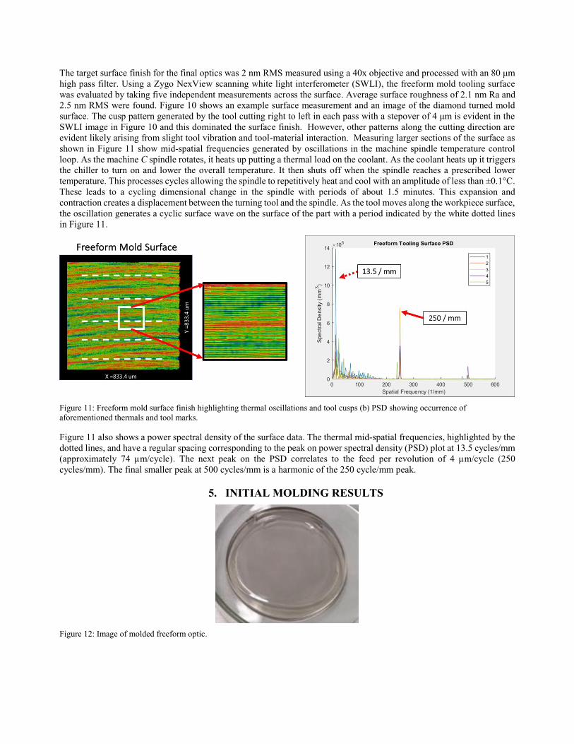
5. INITIAL MOLDING RESULTS
Figure 12: Image of molded freeform optic.

The first prototype molded freeform optic is shown in Figure 12. Using a Zygo NexView, the surface of the optics was
evaluated and compared to the mold tooling. Figure 13 shows a comparison between the mold surface and the prototype
surface. Both surfaces yielded an average of 2 nm average Ra and 3 nm average RMS. However, the glass surface shows
some additional high-frequency content. Further research is required to determine its origin.
Figure 13: Comparison of surface finish (40x) of freeform mold and glass molded freeform.
6. DISCUSSION
Glass molding is a viable process for mass-manufacturing visible light transmissive optics. With the tolerance requirements
of freeform optics and their non-axisymmetric shape, process development is challenging. To our knowledge, this is the
first research to address the issues with precision glass molding of freeform optics. Each step of the precision glass molding
process contains potential error sources. Beginning with manufacture of the mold tooling, validation of mold tooling
dimensions and form. Tolerances on the OD were validated initially with a Tesa CMM and then cross-validated at
LightPath Technologies. After being electroless nickel plated, the tooling was diamond turned through coordinated axis
machining. Temperature control cycling on the machine led to mid-spatial frequencies on the surface of the manufacturing
equipment. Measurements of the mold tooling and molded optics through SWLI display surface roughness in the range of
3 nm RMS and this is in agreement with theoretical estimates. The similarity between the mold tooling surface and the
optics shows that the mold is being replicated into the glass surface to the sub-micrometer scale. Although tool marks are
nearly inevitable without post-polishing, mid-spatial frequency errors due to thermal cycling can be mitigated by addition
of a thermal attenuator. Further research is required, but prototypes have been designed and tested.
After diamond turning the electroless nickel plating, form was measured using a Mahr MahrSurf LD260. Through
MATLAB® processing of the “ideal” and “measured” data grids, a form error of 10 μm PV was found. Rigid body
rotations and translations were introduced to the data to minimize the deviation between the data and the prescription.
However, we have not yet compensated for thermal drift, probe displacements due to surface forces and errors due to
uncertainty in the ball probe radius. Further analysis is required to trace and remove these error sources. Lastly, the glass
molding errors are still being evaluated. With such large diameter optics, flow across the surface could be a limitation on
cycle times. Various glass preform geometries and surface finishes are still under investigation. With surface finish and
size of preforms having the potential to affect the stresses and finish of the glass mold, these are also variables to be
evaluated. Metrology of the optics is the final step to analyze the mold form replication within the optics. An end goal it
to use the computer generated holographic (CGH) null method to measure the form of the optics. However, this requires
a form deviation of a micrometer or less. Since form errors are currently greater than one micrometer form errors are being
evaluated with optical and tactile profilometry. Further iterations of process development are the subject of future research.

ACKNOWLEDGEMENTS
This research was supported by the NSF/I/UCRC Center for Freeform Optics (IIP-1338877 and IIP-1338898). We
acknowledge substantial project motivation, support and guidance from Dr. Eckhard Roth and Dr. Christian Schindler
from Carl Zeiss Jena GmbH. We also acknowledge Dr. Christoph Menke from Carl Zeiss AG for overall project
motivation and helpful input on this paper. We acknowledge the continued support of the Center for Precision
Metrology, in particular Dr. Chris Evans and Mr. Greg Caskey for technical guidance on metrology and for conducting
the profilometer measurements. Finally, we acknowledge Dr. François Piché for his comprehensive review of this
paper.
REFERENCES
1. K. P. Thompson and J. P. Rolland, “Freeform Optical Surfaces: A Revolution in Imaging Optical Design,” Opt.
Photonics News (2012) [doi:10.1364/OPN.23.6.000030].
2. J. R. Troutman, D. L. Barnhardt, J. A. Shultz, J. D. Owen, S. DeFisher, M. A. Davies, and T. J. Suleski,
“Machining and Metrology of a Chalcogenide Glass Freeform Lens Pair,” Procedia Manuf. (2016)
[doi:10.1016/j.promfg.2016.08.055].
3. J. D. Owen, M. A. Davies, D. Schmidt, and E. H. Urruti, “On the ultra-precision diamond machining of
chalcogenide glass,” CIRP Ann. - Manuf. Technol. 64(1), 113–116, CIRP (2015)
[doi:10.1016/j.cirp.2015.04.065].
4. J. D. Owen, J. R. Troutman, T. A. Harriman, A. Zare, Y. Q. Wang, D. A. Lucca, and M. A. Davies, “The
mechanics of milling of germanium for IR applications,” CIRP Ann. - Manuf. Technol. (2016)
[doi:10.1016/j.cirp.2016.04.076].
5. X. H. Zhang, Y. Guimond, and Y. Bellec, “Production of complex chalcogenide glass optics by molding for
thermal imaging,” J. Non. Cryst. Solids 326–327, 519–523, North-Holland (2003) [doi:10.1016/S0022-
3093(03)00464-2].
6. R. O. Maschmeyer, C. A. Andrysick, T. W. Geyer, H. E. Meissner, C. J. Parker, and L. M. Sanford, “Precision
molded-glass optics,” Appl. Opt. 22(16), 2410, Optical Society of America (1983) [doi:10.1364/AO.22.002410].
7. L. Zhang, G. Liu, X. Zhao, O. Dambon, F. Klocke, and A. Y. Yi, “Precision molding of optics: a review of its
development and applications,” 994906 (2016) [doi:10.1117/12.2237968].
8. J. H. Webb, “Apparatus for Molding Lenses,” 2410616, p. 6, United States of America (1943).
9. L. Su, Y. Chen, A. Y. Yi, F. Klocke, and G. Pongs, “Refractive index variation in compression molding of
precision glass optical components,” Appl. Opt. 47(10), 1662–1667, Optical Society of America (2008)
[doi:10.1364/AO.47.001662].
10. A. Y. Yi, C. Huang, F. Klocke, C. Brecher, G. Pongs, M. Winterschladen, A. Demmer, S. Lange, T. Bergs, M.
Merz, and F. Niehaus, “Development of a compression molding process for three-dimensional tailored free-form
glass optics.,” Appl. Opt. 45(25), 6511–6518, Optical Society of America (2006) [doi:10.1364/AO.45.006511].
11. G. Cogburn, L. Mertus, and A. Symmons, “Molding aspheric lenses for low-cost production versus diamond
turned lenses,” Proc. SPIE 7660, B. F. Andresen, G. F. Fulop, and P. R. Norton, Eds., 766020, International
Society for Optics and Photonics (2010) [doi:10.1117/12.850518].
12. “LightPath,” <www.lightpath.com>.
13. F. Z. Z. Fang, X. D. D. Zhang, A. Weckenmann, G. X. X. Zhang, and C. Evans, “Manufacturing and
measurement of freeform optics,” CIRP Ann. - Manuf. Technol. 62(2), 823–846, CIRP (2013)
[doi:10.1016/j.cirp.2013.05.003].
14. L. Alvarez, “Two-Element Variable-Power Spherical Lens,” 3305294, p. 6, United States of America (1964).
15. J. D. Owen, “Manufacture of Infared Optics in Brittle Materials,” University of North Carolina - Charlotte
(2015).
16. J. R. Troutman, “Cutting Mechanics and Manufacture of Optics for Imaging Applications,” University of North
Carolina - Charlotte (2016).