PRACTICAL WORKBOOK - · PDF fileto some special purpose registers only accessible to the...
27
1 PRACTICAL WORKBOOK Computer Architecture and Organization Name : ________________________ Year : ________________________ Batch : ________________________ Roll No : ________________________ Department of Computer Engineering University of Lahore Designed and Compiled by : Engineer Zahid Muneer
Transcript of PRACTICAL WORKBOOK - · PDF fileto some special purpose registers only accessible to the...

1
PRACTICAL WORKBOOK
Computer Architecture and Organization
Name : ________________________
Year : ________________________
Batch : ________________________
Roll No : ________________________
Department of Computer Engineering
University of Lahore
Designed and Compiled by : Engineer Zahid Muneer

2
Contents
LAB 1:Exploring Instruction Set Architecture (ISA) of x86 Machines. ........................................................................... 3
Lab 2 : Introduction to Assembly Language .................................................................................................................. 9
LAB 3: ADDRESSING MODES ....................................................................................................................................... 13
LAB 4: REGISTER INDIRECT ADDRESSING .................................................................................................................... 17
LAB 5: Branching ......................................................................................................................................................... 19
LAB 6: SORTING ........................................................................................................................................................... 23
LAB 7: Bit Manipulations ............................................................................................................................................. 25

3
LAB 1:Exploring Instruction Set Architecture (ISA) of x86 Machines.
1.THEORY
1.1 Instruction Set Architecture (ISA)
The ISA of a machine is the set of its attributes a system programmer needs to know in order to develop system
software or a complier requires for translation of a High Level Language (HLL) code into machine language.
Examples of such attributes are (but not limited to):
Instruction Set
Programmer Accessible Registers - these are the general purpose registers (GPR) within a processor in contrast
to some special purpose registers only accessible to the system hardware and Operating System (OS)
Memory-Processor Interaction
Addressing Modes - means of specifying operands in an instruction (e.g. immediate mode, direct mode, indirect
mode, etc )
Instruction Formats – breakup of an instruction into various fields (e.g. opcode, specification of source and
destination operands, etc)
ISA is also known as the programmer’s view or software model of the machine.
1.2 ISA of x86 Machines
From its onset in 1978, x86 ISA has been the most dominant in desktops and laptops. This represents a family of
machines beginning with 16-bit 8086/8088 microprocessors. (An n-bit microprocessor is capable of performing n-
bit operations). As an evolutionary process, Intel continued to add capabilities and features to this basic ISA. The
80386 was the first 32-bit processor of the family. The ISA of 32-bit processor is regarded as IA-32 (IA for Intel
Architecture) or x86-32 by Intel. IA-64 was introduced in Pentium-4F and later processors. Operating Systems are
now also categorized on the basis of the architecture they can run on. A 64-bit OS can execute both 64-bit and 32-
bit applications. We will limit scope of our discussion to IA-32.
1.2.1 Registers
Registers are storage locations inside the processor. A register can be accessed more quickly than a memory
location. Different registers serve different purposes. Some of them are described below:
1.2.1.1 General-Purpose Registers
EAX, EBX, ECX and EDX are called data or general purpose registers. (E is for extended as they are 32-bit
extensions of their 16-bit counter parts AX, BX, CX and DX in 16-bit ISA). The register EAX is also known as
accumulator because it is used as destination in many arithmetic operations. Some instructions generate more
efficient code if they reference the EAX register rather than other registers.

4
Bits in a register are conventionally numbered from right to left, beginning with 0 as shown below.
31 30 29 - - - 3 2 1 0
Apart from accessing the register as a whole, these registers can be accessed in pieces as illustrated in Fig 1-1.
8 8
AH AL
8 bits + 8 bits
AX 16 bits
Fig. 1-1
It should be carefully noted that high-order 16 bits of these registers cannot be referenced independently.
1.2.1.2 Index Registers
ESI(Extended Source Index) and EDI(Extended Destination Index) registers are respectively used as source and
destination addresses in string operations. They can also be used to implement array indices.
1.2.1.3 Pointer Registers
The EIP (Extended Instruction Pointer) register contains the offset in the current code segment for the next
instruction to be executed. (Segments will be explained shortly).
ESP(Extended Stack Pointer) and EBP(Extended Base Pointer) are used to manipulate stack - a memory area
reserved for holding parameters and return address for procedure calls. ESP holds address of top of stack,
location where the last data item was pushed. EBP is used in procedure calls to hold address of a reference point
in the stack.
1.2.1.4 Flags Register
EFLAGS register is never accessed as a whole. Rather, individual bits of this register either control the CPU
operation (control flags) or reflect the outcome of a CPU operation (status flag). Table 1-1 gives some of the
commonly used control and status flags.
EAX 32 bits

5
Table 1-1
Bit Name of Flag Type Description
11 OF (Overflow Flag) Status Indicates overflow resulting from some arithmetic operation
10
DF (Direction Flag)
Contro
l
Determines left or right direction for moving or comparing string
(character) data.
9
IF (Interrupt Flag)
Contro
l
Indicates that all external interrupts, such as keyboard entry, are to be
processed or ignored.
8 TF (Trap Flag)
Contro
l Permits operation of the processor in single-step mode.
7
SF (Sign Flag)
Status
Contains the resulting sign of an arithmetic operation (0 = positive and 1
= negative).
6
ZF (Zero Flag)
Status
Indicates the result of an arithmetic or comparison operation (0 = nonzero
and 1 = zero result)
4 AF (Auxiliary Flag) Status Contains a carry out of bit 3 on 8–bit data, for specialized arithmetic.
2 Parity Flag (PF) Status Indicates even or odd parity of a low-order (rightmost) 8-bits of data
Contains carry from a high-order (leftmost) bit following an arithmetic
0 CF (Carry Flag) Status operation; also, contains the contents of the last bit of a shift or rotate
operation.
1.2.2Memory Addressing
A 32-bit processor uses 32-bit addresses and thus can access 232
B = 4GB physical memory. Depending on the
machine, a processor can access one or more bytes from memory at a time. The number of bytes accessed
simultaneously from main memory is called word length of machine.
Generally, all machines are byte-addressable i.e.; every byte stored in memory has a unique address. However,
word length of a machine is typically some integral multiple of a byte. Therefore, the address of a word must be the
address of one of its constituting bytes. In this regard, one of the following methods of addressing (also known as
byte ordering) may be used.
Big Endian – the higher byte is stored at lower memory address (i.e. Big Byte first). MIPS, Apple, Sun SPARC are
some of the machines in this class.

6
Little Endian - the lower byte is stored at lower memory address (i.e. Little Byte first). Intel’s machines use little
endian.
Consider for example, storing 0xA2B1C3D4 in main memory. The two byte orderings are illustrated in Fig. 1-2.
Addresses Contents Addresses Contents
2032 A2 2032 D4
2033 B1 2033 C3
2034 C3 2034 B1
2035 D4 2035 A2
BIG Endian LITTLE Endian
Fig. 1-2
1.2.3 Memory Models
IA-32 can use one of the three basic memory models:
Flat Memory Model – memory appears to a program as a single, contiguous address space of 4GB. Code, data,
and stack are all contained in this address space, also called the linear address space
Segmented Memory Model – memory appears to a program as a group of independent memory segments, where
code, data, and stack are contained in separate memory segments. To address memory in this model, the processor
must use segment registers and an offset to derive the linear address. The primary reason for having segmented
memory is to increase the system's reliability by means of protecting one segment from other.
Real-Address Memory Model – is the original 8086 model and its existence ensures backward compatibility.
1.2.4 Segment Registers
The segment registers hold the segment selectors which are special pointers that point to start of individual
segments in memory. The use of segment registers is dependent on the memory management model in use.
In a flat memory model, segment registers point to overlapping segments, each of which begins at address 0 as
illustrated in Fig. 1-3. When using the segmented memory model, each segment is loaded with a different memory
address (Fig. 1-4).
The segment registers (CS, DS, SS, ES, FS, and GS) hold 16-bit segment selectors. To access a particular segment
in memory, the segment selector for that segment must be present in the appropriate segment register. Each of the
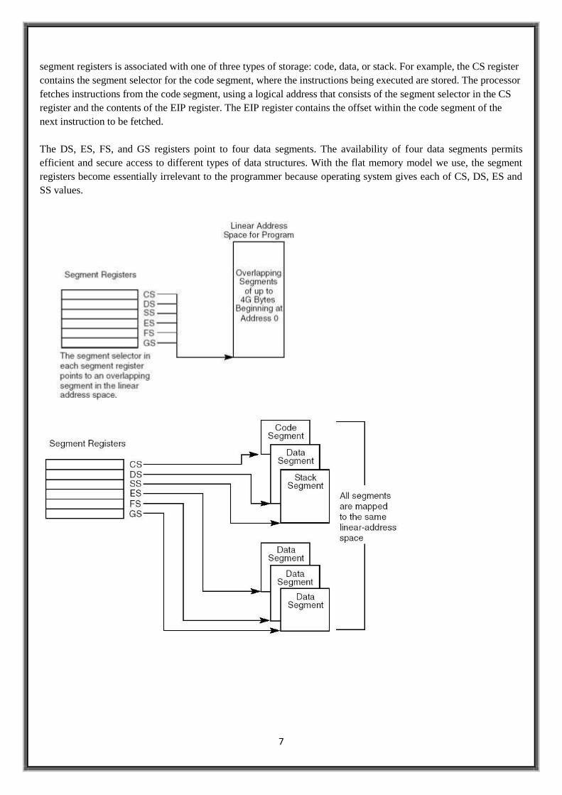
7
segment registers is associated with one of three types of storage: code, data, or stack. For example, the CS register
contains the segment selector for the code segment, where the instructions being executed are stored. The processor
fetches instructions from the code segment, using a logical address that consists of the segment selector in the CS
register and the contents of the EIP register. The EIP register contains the offset within the code segment of the
next instruction to be fetched.
The DS, ES, FS, and GS registers point to four data segments. The availability of four data segments permits
efficient and secure access to different types of data structures. With the flat memory model we use, the segment
registers become essentially irrelevant to the programmer because operating system gives each of CS, DS, ES and
SS values.

8
3. EXERCISES
1.Fill in the following tables to show storage of 0xABDADDBA at address 1996 in the memory of a machine
using (i) little endian (ii) big endian byte ordering.
Addresses Contents Addresses Contents
1996
1996
1997
1997
1998
1998
1998
1998
LITTLE Endian BIG Endian
2.What is the significance of learning ISA of a processor?
3.Show the ECX register and the size and position of the CH, CL, and CX within it.

9
Lab 2 : Introduction to Assembly Language
2.1 BASIC COMPUTER ARCHITECTURE
A computer system comprises of a processor, memory, and I/O devices. I/O is used for interfacing with the
external world, while memory is the processor’s internal world. Processor is the core in this picture and is
responsible for performing operations. The operation of a computer can be fairly described with processor and
memory only. Now the whole working of the computer is performing an operation by the processor on data, which
resides in memory. The scenario that the processor executes operations and the memory contains data elements
requires a mechanism for the processor to read that data from the memory.
• There must be a mechanism to inform memory that we want to do the read operation.
• There must be a mechanism to inform memory that we want to read precisely which element
• There must be a mechanism to transfer that data element from memory to processor
The group of bits that the processor uses to inform the memory about which element to read or write is collectively
known as the address bus. Another important bus called the data bus is used to move the data from the memory to
the processor in a read operation and from the processor to the memory in a write operation. The third group
consists of miscellaneous independent lines used for control purposes. For example, one line of the bus is used to
inform the memory about whether to do the read operation or the write operation. These lines are collectively
known as the control bus.
2.1.1 REGISTERS
The basic purpose of a computer is to perform operations, and operations need operands. Operands are the
data on which we want to perform a certain operation. Consider the addition operation; it involves adding two
numbers to get their sum. We can have precisely one address on the address bus and consequently precisely one
element on the data bus. At the very same instant the second operand cannot be brought inside the processor. As
soon as the second is selected, the first operand is no longer there. For this reason there are temporary storage
places inside the processor called registers. Now one operand can be read in a register and added into the other
which is read directly from the memory.
Registers are like a scratch pad ram inside the processor and their operation is very much like normal
memory cells. They have precise locations and remember what is placed inside them. They are used when we need
more than one data element inside the processor at one time. The concept of registers will be further elaborated as
we progress into writing our first program. Memory is a limited resource but the number of memory cells is large.
Registers are relatively very small in number, and are therefore a very scarce and precious resource. Registers are
more than one in number, so we have to precisely identify or name them.

10
2.1.2 REGISTER ARCHITECTURE
CS
DS
SS
ES
IP
FLAGS
General Registers (AX, BX, CX, and DX)
The registers AX, BX, CX, and DX behave as general purpose registers in Intel architecture and do some specific
functions in addition to it. X in their names stand for extended meaning 16bit registers. For example AX means we
are referring to the extended 16bit “A” register. Its upper and lower byte are separately accessible as AH (A high
byte) and AL (A low byte). All general purpose registers can be accessed as one 16bit register or as two 8bit
registers. The two registers AH and AL are part of the big whole AX. Any change in AH or AL is reflected in AX
as well. AX is a composite or extended register formed by gluing together the two parts AH and AL. The A of AX
stands for Accumulator. Even though all general purpose registers can act as accumulator in most instructions there
are some specific variations which can only work on AX which is why it is named the accumulator. The B of BX
stands for Base because of its role in memory addressing as discussed in the next chapter. The C of CX stands for
Counter as there are certain instructions that work with an automatic count in the CX register. The D of DX stands
for Destination as it acts as the destination in I/O operations. The A, B, C, and D are in letter sequence as well as
depict some special functionality of the register.
Index Registers (SI and DI)
SI and DI stand for source index and destination index respectively. These are the index registers of the Intel
architecture which hold address of data and used in memory access. Being an open and flexible architecture, Intel
allows many mathematical and logical operations on these registers as well like the general registers. The source
and destination are named because of their implied functionality as the source or the destination in a special class of
instructions called the string instructions. However their use is not at all restricted to string instructions. SI and DI
are 16bit and cannot be used as 8bit register pairs like AX, BX, CX, and DX.
Instruction Pointer (IP)
This is the special register containing the address of the next instruction to be executed. No mathematics or memory
access can be done through this register. It is out of our direct control and is automatically used. Playing with it is
dangerous and needs special care. Program control instructions change the IP register.
Stack Pointer (SP)
It is a memory pointer and is used indirectly by a set of instructions. This register will be explored in the discussion
of the system stack.
Base Pointer (BP)
It is also a memory pointer containing the address in a special area of memory called the stack and will be explored
alongside SP in the discussion of the stack.
SP
BP
SI
DI
AH AL AX
BH BL BX
CH CL CX
DH DL DX

11
OUR FIRST PROGRAM IN ASSEMBLY
The first program that we will write will only add three numbers. This very simple program will clarify most of the
basic concepts of assembly language. We will start with writing our algorithm in English and then moving on to
convert it into assembly language.
move 5 to ax
move 10 to bx
add bx to ax
move 15 to bx
add bx to ax
Even in this simple reflection of thoughts in English, there are some key things to observe. One is the concept of
destination as every instruction has a “to destination” part and there is a source before it as well.
Assembly Language Version
Intel could have made their assembly language exactly identical to our program in plain English but they have
abbreviated a lot of symbols to avoid unnecessarily lengthy program when the meaning could be conveyed with
less effort. For example Intel has named their move instruction “mov” instead of “move.” Similarly the Intel order
of placing source and destination is opposite to what we have used in our English program, just a change of
interpretation. So the Intel way of writing things is:
operation destination, source
Example 2.1
; a program to add three numbers using registers
mov ax, 5 ; load first number in ax
mov bx, 10 ; load second number in bx
add ax, bx ; accumulate sum in ax
mov bx, 15 ; load third number in bx
add ax, bx ; accumulate sum in ax
To start a comment a semicolon is used and the assembler ignores everything else on the same line. Comments
must be extensively used in assembly language programs to make them readable.
Assembler, Linker, and Debugger
We need an assembler to assemble this program and convert this into executable binary code. The assembler that
we will use during this course is MASM.
CLASS EXERCISE
1. Write instructions that perform the following operations.
a. Copy BL into CL
b. Copy DX into AX
c. Store 0x12 into AL
d. Store 0x1234 into AX
e. Store 0xFFFF into AX
2. Write a program in assembly language that calculates the square of six by adding six to the accumulator six
times.
12
3. A combination of 8bits is called a byte. What is the name for 4bits and for 16bits?
4. What are registers and what are the specific features of the accumulator, index registers and program counter?
5. Give the value of the zero flag, the carry flag, the sign flag, and the overflow flag after each of the following
instructions if AX is initialized with 0x1254 and BX is initialized with 0x0FFF.
a. add ax, 0xEDAB
b. add ax, bx
c. add bx, 0xF001

13
LAB 3: ADDRESSING MODES 3.1 DATA DECLARATION
The first instruction of our first assembly language program was “mov ax, 5.” Here MOV was the opcode;
AX was the destination operand, while 5 was the source operand. The value of 5 in this case was stored as part of
the instruction encoding. In the opcode B80500, B8 was the opcode and 0500 was the operand stored immediately
afterwards. Such an operand is called an immediate operand. It is one of the many types of operands available.
Writing programs using just the immediate operand type is difficult. Every reasonable program needs some data in
memory apart from constants. Constants cannot be changed, i.e. they cannot appear as the destination operand. In
fact placing them as destination is meaningless and illegal according to assembly language syntax. Only registers or
data placed in memory can be changed. So real data is the one stored in memory, with a very few constants. So
there must be a mechanism in assembly language to store and retrieve data from memory.
To declare a part of our program as holding data instead of instructions we need a couple of very basic but
special assembler directives. The first directive is “define byte” written as “db.”
db some value
As a result a cell in memory will be reserved containing the desired value in it and it can be used in a variety of
ways. Now we can add variables instead of constants. The other directive is “define word” or “dw” with the same
syntax as “db” but reserving a whole word of 16 bits instead of a byte. There are directives to declare a double or a
quad word as well but we will restrict ourselves to byte and word declarations for now. For single byte we use db
and for two bytes we use dw.
3.1.1 Data allocation
The general format of a storage allocator is:
[variable-name] define-directive initial-value [,initial-value],...
Variable-name: identify the storage space allocated.
Define-directive: the following table shows the directives that can be used, and the size in bytes:
Directive Description of Initializers
BYTE, DB (byte) Allocates unsigned numbers from 0 to 255.
SBYTE (signed byte) Allocates signed numbers from –128 to +127.
WORD, DW (word = 2 bytes) Allocates unsigned numbers from 0 to 65,535
(64K).
SWORD (signed word) Allocates signed numbers from –32,768 to
+32,767.
DWORD, DD (doubleword = 4 bytes), Allocates unsigned numbers from 0 to
4,294,967,295 (4 megabytes).
SDWORD (signed doubleword) Allocates signed numbers from –2,147,483,648 to
+2,147,483,647.
FWORD, DF (farword = 6 bytes) Allocates 6-byte (48-bit) integers. These values are
normally used only as pointer variables on the
80386/486 processors.
QWORD, DQ (quadword = 8 bytes) Allocates 8-byte integers used with 8087-family
coprocessor instructions.
TBYTE, DT (10 bytes), Allocates 10-byte (80-bit) integers if the initializer
has a radix specifying the base of the number.
REAL4 Short (32-bit) real numbers
REAL8 Long (64-bit) real numbers
14
REAL10 10-byte (80-bit) real numbers and BCD numbers
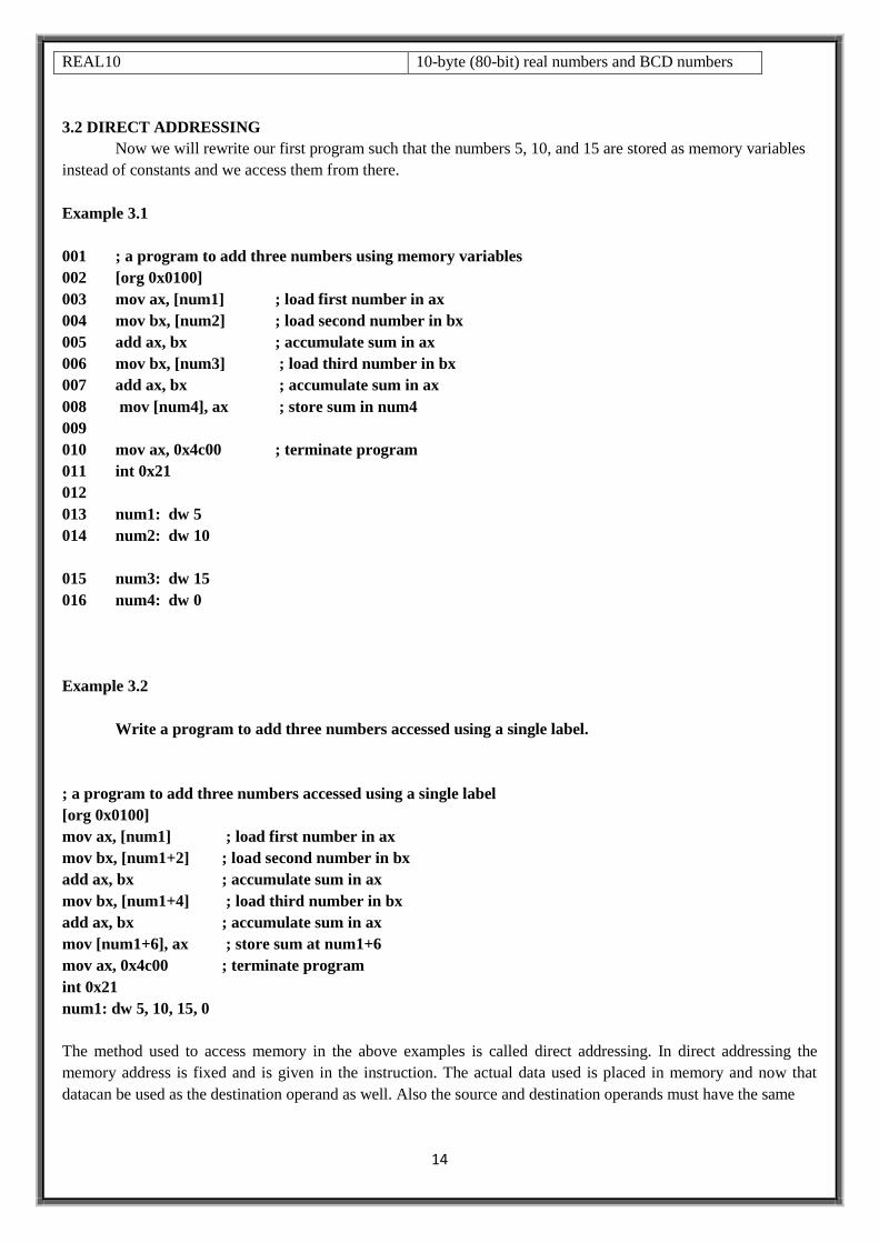
3.2 DIRECT ADDRESSING
Now we will rewrite our first program such that the numbers 5, 10, and 15 are stored as memory variables
instead of constants and we access them from there.
Example 3.1
001 ; a program to add three numbers using memory variables
002 [org 0x0100]
003 mov ax, [num1] ; load first number in ax
004 mov bx, [num2] ; load second number in bx
005 add ax, bx ; accumulate sum in ax
006 mov bx, [num3] ; load third number in bx
007 add ax, bx ; accumulate sum in ax
008 mov [num4], ax ; store sum in num4
009
010 mov ax, 0x4c00 ; terminate program
011 int 0x21
012
013 num1: dw 5
014 num2: dw 10
015 num3: dw 15
016 num4: dw 0
Example 3.2
Write a program to add three numbers accessed using a single label.
; a program to add three numbers accessed using a single label
[org 0x0100]
mov ax, [num1] ; load first number in ax
mov bx, [num1+2] ; load second number in bx
add ax, bx ; accumulate sum in ax
mov bx, [num1+4] ; load third number in bx
add ax, bx ; accumulate sum in ax
mov [num1+6], ax ; store sum at num1+6
mov ax, 0x4c00 ; terminate program
int 0x21
num1: dw 5, 10, 15, 0
The method used to access memory in the above examples is called direct addressing. In direct addressing the
memory address is fixed and is given in the instruction. The actual data used is placed in memory and now that
datacan be used as the destination operand as well. Also the source and destination operands must have the same

15
size. For example a word defined memory is read in a word sized register. A last observation is that the data 0500
in memory was corrected to 0005 when read in a register. So registers contain data in proper order as a word.
A last variation using direct addressing shows that we can directly add a memory variable and a register instead of
adding a register into another that we were doing till now.
EXAMPLE 3.3
Write a program to add three numbers directly in memory
mov ax, [num1] ; load first number in ax
mov [num1+6], ax ; store first number in result
mov ax, [num1+2] ; load second number in ax
add [num1+6], ax ; add second number to result
mov ax, [num1+4] ; load third number in ax
add [num1+6], ax ; add third number to result
mov ax, 0x4c00 ; terminate program
int 0x21
num1: dw 5, 10, 15, 0
The opcode of add is changed because the destination is now a memory location instead of a register. No other
significant change is seen in the listing file. Inside the debugger we observe that few opcodes are longer nowand the
location num1 is now translating to 0119 instead of 0117. This isdone automatically by the assembler as a result of
using labels instead ofhard coding addresses. During execution we observe that the word data as it is read into a
register is read in correct order. The significant change in this example is that the destination of addition is memory.
Method to access memory is direct addressing, whether it is the MOV instruction or the ADD instruction.
The first two instructions of the last program read a number into AX and placed it at another memory location. A
quick thought reveals that the following might be a possible single instruction to replace the couple.
mov [num1+6], [num1] ; ILLEGAL
However this form is illegal and not allowed on the Intel architecture. None of the general operations of mov add,
sub etc. allow moving data from memory to memory. Only register to register, register to memory, memory to
register, constant to memory, and constant to register operations are allowed. The other register to constant,
memory to constant, and memory to memory are all disallowed.
Class exercise:
1.write a program in assembly that add 10 numbers directly in memory using direct addressing mod.
2.Write a program assembly that add three number using byte variables.

16
3.what is the effect of following instruction on flag registers OF, Carry flag
Zero flag, Sign flag.
1. mov al,+127 3. mov al,0FFh
add al,1 add al,1
2. mov al,-128 4. mov cx,1
sub al,1 sub cx,1
5. mov ax,0FFFFh
inc ax

17
LAB 4: REGISTER INDIRECT ADDRESSING 4.1 INDIRECT ADDRESSING
We have done very elementary data access till now. Assume that the numbers we had were 100 and not just
three. This way of adding them will cost us 200 instructions. There must be some method to do a task repeatedly on
data placed in consecutive memory cells. The key to this is the need for some register that can hold the address of
data. So that we can change the address to access some other cell of memory using the same instruction. In direct
addressing mode the memory cell accessed was fixed inside the instruction. There is another method in which the
address can be placed in a register so that it can be changed. For the following example we will take 10 instead of
100 numbers but the algorithm is extensible to any size. There are four registers in X88 architecture that can hold
address of data and they are BX, BP, SI, and DI. There are minute differences in their working which will be
discussed later. For the current example, we will use the BX register and we will take just three numbers and extend
the concept with more numbers in later examples.
EXAMPLE 4.1
Adding three no using indirect addressing
num1: dw 5, 10, 15, 0
mov bx, offset num1 ; point bx to first number
mov ax, [bx] ; load first number in ax
add bx, 2 ; advance bx to second number
add ax, [bx] ; add second number to ax
add bx, 2 ; advance bx to third number
add ax, [bx] ; add third number to ax
add bx, 2 ; advance bx to result
mov [bx], ax ; store sum at num1+6
mov ax, 0x4c00 ; terminate program
int 0x21
Observe that no square brackets around num1 are used this time. The address is loaded in bx and not the
contents.
Brackets are now used around BX. mov ax, [bx]The instruction will be read as “move into ax the contents
of the memory location whose address is in bx.” Now since bx contains the address of num1 the contents of
num1 are transferred to the ax register.
This instruction add bx, 2 is changing the address. Since we have words notbytes, we add two to bx so that
it points to the next word in memory.
4.2. REGISTER + OFFSET ADDRESSING
Direct addressing and indirect addressing using a single register are two basic forms of memory access.
Another possibility is to use different combinations of direct and indirect references. In the above example we used
BX to access different array elements which were placed consecutively in memory like an array. We can also place
in BX only the array index and not the exact address and form the exact address when we are going to access the
actual memory. This way the same register can be used for accessing different arrays and also the register can be
used for index comparison like the following example does.
EXAMPLE 4.2
num1: dw 10, 20, 30, 40, 50, 10, 20, 30, 40, 50
total: dw 0
mov si, 0 ; initialize array index to zero
mov cx, 10 ; load count of numbers in cx
mov ax, 0 ; initialize sum to zero
l1: add ax, [num1+si] ; add number to ax

18
add si, 2 ; advance bx to next index
sub cx, 1 ; numbers to be added reduced
jnz l1 ; if numbers remain add next
mov [total], ax ; write back sum in memory
CLASS EXERCISE
1. Differentiate between effective address and physical address.
2.Write instructions to do the following.
a. Copy contents of memory location with offset 0025 in the current data segment into AX.
b. Copy AX into memory location with offset 0FFF in the current data segment.
c. Move contents of memory location with offset 0010 to memory location with offset 002F in the current
data segment.
3. Write a program to calculate the square of 20 by using a loop that adds 20 to the accumulator 20 times.
4.write a program that load eax with variable which content are placed in memory and show the NEG
instruction effect on overflow flag when the content of variable are signed number.
19
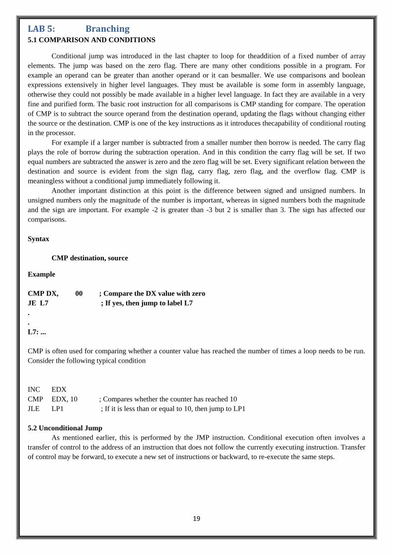
LAB 5: Branching 5.1 COMPARISON AND CONDITIONS
Conditional jump was introduced in the last chapter to loop for theaddition of a fixed number of array
elements. The jump was based on the zero flag. There are many other conditions possible in a program. For
example an operand can be greater than another operand or it can besmaller. We use comparisons and boolean
expressions extensively in higher level languages. They must be available is some form in assembly language,
otherwise they could not possibly be made available in a higher level language. In fact they are available in a very
fine and purified form. The basic root instruction for all comparisons is CMP standing for compare. The operation
of CMP is to subtract the source operand from the destination operand, updating the flags without changing either
the source or the destination. CMP is one of the key instructions as it introduces thecapability of conditional routing
in the processor.
For example if a larger number is subtracted from a smaller number then borrow is needed. The carry flag
plays the role of borrow during the subtraction operation. And in this condition the carry flag will be set. If two
equal numbers are subtracted the answer is zero and the zero flag will be set. Every significant relation between the
destination and source is evident from the sign flag, carry flag, zero flag, and the overflow flag. CMP is
meaningless without a conditional jump immediately following it.
Another important distinction at this point is the difference between signed and unsigned numbers. In
unsigned numbers only the magnitude of the number is important, whereas in signed numbers both the magnitude
and the sign are important. For example -2 is greater than -3 but 2 is smaller than 3. The sign has affected our
comparisons.
Syntax
CMP destination, source
Example
CMP DX, 00 ; Compare the DX value with zero
JE L7 ; If yes, then jump to label L7
.
.
L7: ...
CMP is often used for comparing whether a counter value has reached the number of times a loop needs to be run.
Consider the following typical condition
INC EDX
CMP EDX, 10 ; Compares whether the counter has reached 10
JLE LP1 ; If it is less than or equal to 10, then jump to LP1
5.2 Unconditional Jump
As mentioned earlier, this is performed by the JMP instruction. Conditional execution often involves a
transfer of control to the address of an instruction that does not follow the currently executing instruction. Transfer
of control may be forward, to execute a new set of instructions or backward, to re-execute the same steps.

20
Syntax
The JMP instruction provides a label name where the flow of control is transferred immediately. The syntax of the
JMP instruction is −
JMP label
5.3 Conditional Jump
If some specified condition is satisfied in conditional jump, the control flow is transferred to a target
instruction. There are numerous conditional jump instructions depending upon the condition and data.Following
are the conditional jump instructions used on signed data used for arithmetic operations −
Instruction Description Flags tested
JE/JZ Jump Equal or Jump Zero ZF
JNE/JNZ Jump not Equal or Jump Not Zero ZF
JG/JNLE Jump Greater or Jump Not Less/Equal OF, SF, ZF
JGE/JNL Jump Greater or Jump Not Less OF, SF
JL/JNGE Jump Less or Jump Not Greater/Equal OF, SF
JLE/JNG Jump Less/Equal or Jump Not Greater OF, SF, ZF
Following are the conditional jump instructions used on unsigned data used for logical operations −
Instruction Description Flags tested
JE/JZ Jump Equal or Jump Zero ZF
JNE/JNZ Jump not Equal or Jump Not Zero ZF
JA/JNBE Jump Above or Jump Not Below/Equal CF, ZF
JAE/JNB Jump Above/Equal or Jump Not Below CF

21
JB/JNAE Jump Below or Jump Not Above/Equal CF
JBE/JNA Jump Below/Equal or Jump Not Above AF, CF
The following conditional jump instructions have special uses and check the value of flags −
Instruction Description Flags tested
JXCZ Jump if CX is Zero none
JC Jump If Carry CF
JNC Jump If No Carry CF
JO Jump If Overflow OF
JNO Jump If No Overflow OF
JP/JPE Jump Parity or Jump Parity Even PF
JNP/JPO Jump No Parity or Jump Parity Odd PF
JS Jump Sign (negative value) SF
JNS Jump No Sign (positive value) SF
EXAMPLE
program to add ten numbers without a separate counter
num1: dw 10, 20, 30, 40, 50, 10, 20, 30, 40, 50
total: dw 0
mov bx, 0 ; initialize array index to zero
mov ax, 0 ; initialize sum to zero
l1: add ax, [num1+bx] ; add number to ax
add bx, 2 ; advance bx to next index
cmp bx, 20 ; are we beyond the last index

22
jne l1 ; if not add next number
mov [total], ax ; write back sum in memory
EXAMPLE
jmp start ; unconditionally jump over data
num1: dw 10, 20, 30, 40, 50, 10, 20, 30, 40, 50
total: dw 0
start: mov bx, 0 ; initialize array index to zero
mov ax, 0 ; initialize sum to zero
l1: add ax, [num1+bx] ; add number to ax
add bx, 2 ; advance bx to next index
cmp bx, 20 ; are we beyond the last index
jne l1 ; if not add next number
mov [total], ax ; write back sum in memory
Class Exercise
1. Will the following code jump to the label named Target?
mov ax,8109h
cmp ax,26h
jg Target
2. Will the following code jump to the label named Target?
mov ax,-30
cmp ax,-50
jg Target
3. Suppose the CMP instruction compares the integers 7FFFh and 8000h. Show how the JB
and JL instructions would generate different results if used after comparing these values.
4.Write instructions that jump to label L2 when the signed integer in AX is greater than the
integer in CX.

23
LAB 6: SORTING 6.1 SORTING
Moving ahead from our example of adding numbers we progress to a program that can sort a list of
numbers using the tools that we have accumulated till now. Sorting can be ascending or descending like if the
largest number comes at the top, followed by a smaller number and so on till the smallest number the sort will be
called descending. The other order starting with the smallest number and ending at the largest is called ascending
sort. This is a common problem and many algorithms have been developed to solve it. One simple algorithm is the
bubble sort algorithm.
In this algorithm we compare consecutive numbers. If they are in required order e.g. if it is a descending sort and
the first is larger then the second, then we leave them as it is and if they are not in order, we swap them. Then we
do the same process for the next two numbers and so on till the last two are compared and possibly swapped. A
complete iteration is called a pass over the array. We need N passes at least in the simplest algorithm if N is the
number of elements to be sorted. A finer algorithm is to check if any swap was done in this pass and stop as soon as
a pass goes without a swap. The array is now sorted as every pair of elements is in order.
State of Data Swap Done Swap Flag
PASS 1
60 55 45 58 yes On
55 60 45 58 yes On
55 45 60 58 yes On
PASS 2
55 45 58 60 yes On
45 55 58 60 no off
45 55 58 60 no off
PASS 3
45 55 58 60 no off
45 55 58 60 no off
45 55 58 60 no off
EXAMPLE
jmp start
data: dw 60, 55, 45, 50, 40, 35, 25, 30, 10, 0
swap: db 0
start: mov bx, 0 ; initialize array index to zero
mov byte [swap], 0 ; rest swap flag to no swaps
loop1: mov ax, [data+bx] ; load number in ax
cmp ax, [data+bx+2] ; compare with next number

24
jbe noswap ; no swap if already in order
mov dx, [data+bx+2] ; load second element in dx
mov [data+bx+2], ax ; store first number in second
mov [data+bx], dx ; store second number in first
mov byte [swap], 1 ; flag that a swap has been done
noswap: add bx, 2 ; advance bx to next index
cmp bx, 18 ; are we at last index
jne loop1 ; if not compare next two
cmp byte [swap], 1 ; check if a swap has been done
je start ; if yes make another pass
CLASS EXERCISE
1.write a program in assembly that sort the array of data in descending order
where the array of data is 20,12,7,0,57,97,98,55,67,34.
2.Write a program that sort the array of data in ascending and descending order which contained signed and un
signed number as -45,-2,-1,4,56,43,23,-10,0 3,7,8.
25
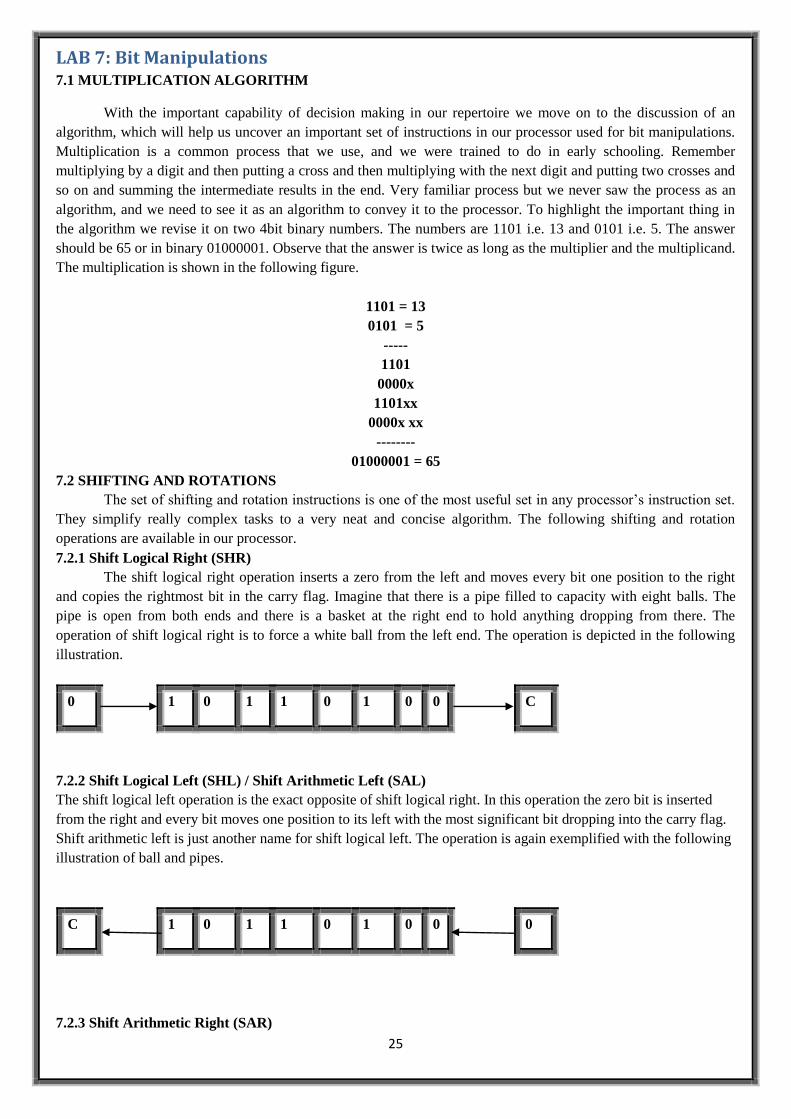
LAB 7: Bit Manipulations 7.1 MULTIPLICATION ALGORITHM
With the important capability of decision making in our repertoire we move on to the discussion of an
algorithm, which will help us uncover an important set of instructions in our processor used for bit manipulations.
Multiplication is a common process that we use, and we were trained to do in early schooling. Remember
multiplying by a digit and then putting a cross and then multiplying with the next digit and putting two crosses and
so on and summing the intermediate results in the end. Very familiar process but we never saw the process as an
algorithm, and we need to see it as an algorithm to convey it to the processor. To highlight the important thing in
the algorithm we revise it on two 4bit binary numbers. The numbers are 1101 i.e. 13 and 0101 i.e. 5. The answer
should be 65 or in binary 01000001. Observe that the answer is twice as long as the multiplier and the multiplicand.
The multiplication is shown in the following figure.
1101 = 13
0101 = 5
-----
1101
0000x
1101xx
0000x xx
--------
01000001 = 65
7.2 SHIFTING AND ROTATIONS
The set of shifting and rotation instructions is one of the most useful set in any processor’s instruction set.
They simplify really complex tasks to a very neat and concise algorithm. The following shifting and rotation
operations are available in our processor.
7.2.1 Shift Logical Right (SHR)
The shift logical right operation inserts a zero from the left and moves every bit one position to the right
and copies the rightmost bit in the carry flag. Imagine that there is a pipe filled to capacity with eight balls. The
pipe is open from both ends and there is a basket at the right end to hold anything dropping from there. The
operation of shift logical right is to force a white ball from the left end. The operation is depicted in the following
illustration.
0 1 0 1 1 0 1 0 0 C
7.2.2 Shift Logical Left (SHL) / Shift Arithmetic Left (SAL)
The shift logical left operation is the exact opposite of shift logical right. In this operation the zero bit is inserted
from the right and every bit moves one position to its left with the most significant bit dropping into the carry flag.
Shift arithmetic left is just another name for shift logical left. The operation is again exemplified with the following
illustration of ball and pipes.
C 1 0 1 1 0 1 0 0 0
7.2.3 Shift Arithmetic Right (SAR)
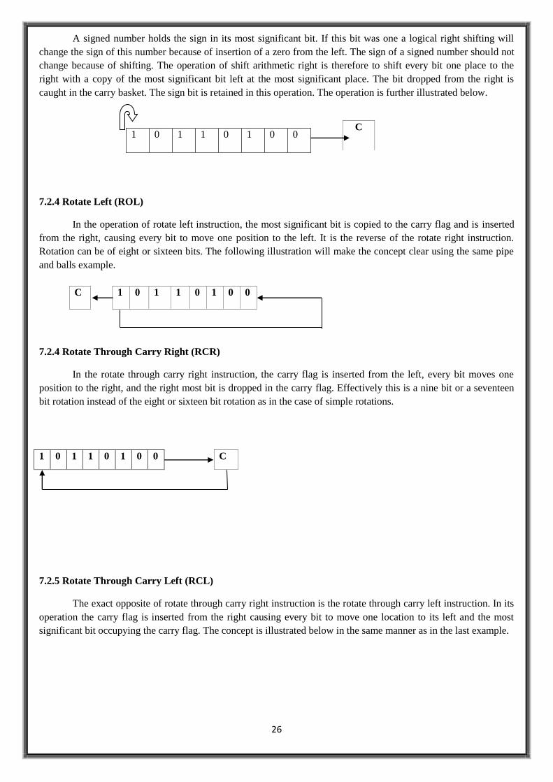
26
A signed number holds the sign in its most significant bit. If this bit was one a logical right shifting will
change the sign of this number because of insertion of a zero from the left. The sign of a signed number should not
change because of shifting. The operation of shift arithmetic right is therefore to shift every bit one place to the
right with a copy of the most significant bit left at the most significant place. The bit dropped from the right is
caught in the carry basket. The sign bit is retained in this operation. The operation is further illustrated below.
7.2.4 Rotate Left (ROL)
In the operation of rotate left instruction, the most significant bit is copied to the carry flag and is inserted
from the right, causing every bit to move one position to the left. It is the reverse of the rotate right instruction.
Rotation can be of eight or sixteen bits. The following illustration will make the concept clear using the same pipe
and balls example.
C 1 0 1 1 0 1 0 0
7.2.4 Rotate Through Carry Right (RCR)
In the rotate through carry right instruction, the carry flag is inserted from the left, every bit moves one
position to the right, and the right most bit is dropped in the carry flag. Effectively this is a nine bit or a seventeen
bit rotation instead of the eight or sixteen bit rotation as in the case of simple rotations.
1 0 1 1 0 1 0 0 C
7.2.5 Rotate Through Carry Left (RCL)
The exact opposite of rotate through carry right instruction is the rotate through carry left instruction. In its
operation the carry flag is inserted from the right causing every bit to move one location to its left and the most
significant bit occupying the carry flag. The concept is illustrated below in the same manner as in the last example.
1 0 1 1 0 1 0 0 C

27
EXAMPLE
4bit multiplication algorithm
jmp start
multiplicand: db 13 ; 4bit multiplicand (8bit space)
multiplier: db 5 ; 4bit multiplier
result: db 0 ; 8bit result
start: mov cl, 4 ; initialize bit count to four
mov bl, [multiplicand] ; load multiplicand in bl
mov dl, [multiplier] ; load multiplier in dl
checkbit: shr dl, 1 ; move right most bit in carry
jnc skip ; skip addition if bit is zero
add [result], bl ; accumulate result
skip: shl bl, 1 ; shift multiplicand left
dec cl ; decrement bit count
jnz checkbit ; repeat if bits left
CLASS EXERCISE
1.Write a program in assembly for 8bit multiplication algorithm. Store the result in memory and also load
the result in accumulator.
2. Write a program in assembly for 16bit multiplication algorithm. Store the result in memory and also load
the result in accumulator.
C 1 0 1 1 0 1 0 0