
Power Supply IC Series for TFT LCD Panels High-precision...
13
1/10 www.rohm.com 2009.07 - Rev.B © 2009 ROHM Co., Ltd. All rights reserved. Power Supply IC Series for TFT LCD Panels High-precision Gamma Correction IC with built-in DAC BD8143MUV ●Description This gamma correction voltage generation IC feature built-in DACs and provide a 1chip solution with setting control via serial communications, a high-precision 10-bitDAC, and Buffer Amp (12ch). ●Features 1) 1chip design means fewer components 2) Built-in 10bit DAC 3) DAC output Buffer AMP (12ch) 4) Amp input select (CTL) 5) 3-line serial interface control 6) Thermal shut down 7) Power ON Reset Circuit 8) VQFN032V5050 Package ●Applications These ICs can be used with TFT LCD Panels used by Large-Screen and High-Definition LCD TVs. ●Absolute maximum ratings (Ta=25℃) Parameter Symbol Limit Unit Power Supply Voltage 1 DVCC 7 V Power Supply Voltage 2 VCC 20 V REFIN Voltage REF 20 V Amplifier Drive Current Io 30 * 1 mA Junction Temperature Tjmax 150 ℃ Power Dissipation Pd 2440 * 2 mW Operating Temperature Range Topr -40~+105 ℃ Storage Temperature Range Tstg -55~+150 ℃ *1 Pd, should not be exceeded. *2 Reduced by 19.52mW/°C over 25°C, when mounted on a glass epoxy board. (4-layer 74.2×74.2×1.6mm). ●Operating Condition (Ta=-40℃~105℃) Parameter Symbol Limit Unit MIN MAX Power Supply Voltage 1 DVCC 2.3 5.5 V Power Supply Voltage 2 VCC 8 18 V REFIN Voltage REF 8 18 V AMP0 Drive Current I OA -40 - mA AMP1~10 Drive Current I OB -20 20 mA AMP11 Drive Current I OC - 40 mA Serial CLK Frequency fCLK - 5 MHz OSC Frequency FOSC - 200 kHz No.09035EBT08
Transcript of Power Supply IC Series for TFT LCD Panels High-precision...

1/10 www.rohm.com 2009.07 - Rev.B
© 2009 ROHM Co., Ltd. All rights reserved.
Power Supply IC Series for TFT LCD Panels
High-precision Gamma Correction IC with built-in DAC BD8143MUV
●Description
This gamma correction voltage generation IC feature built-in DACs and provide a 1chip solution with setting control via serial communications, a high-precision 10-bitDAC, and Buffer Amp (12ch).
●Features 1) 1chip design means fewer components 2) Built-in 10bit DAC 3) DAC output Buffer AMP (12ch) 4) Amp input select (CTL) 5) 3-line serial interface control 6) Thermal shut down 7) Power ON Reset Circuit 8) VQFN032V5050 Package
●Applications
These ICs can be used with TFT LCD Panels used by Large-Screen and High-Definition LCD TVs.
●Absolute maximum ratings (Ta=25℃)
Parameter Symbol Limit Unit
Power Supply Voltage 1 DVCC 7 V
Power Supply Voltage 2 VCC 20 V
REFIN Voltage REF 20 V
Amplifier Drive Current Io 30 *1 mA
Junction Temperature Tjmax 150 ℃
Power Dissipation Pd 2440 *2 mW
Operating Temperature Range Topr -40~+105 ℃
Storage Temperature Range Tstg -55~+150 ℃ *1 Pd, should not be exceeded. *2 Reduced by 19.52mW/°C over 25°C, when mounted on a glass epoxy board. (4-layer 74.2×74.2×1.6mm).
●Operating Condition (Ta=-40℃~105℃)
Parameter Symbol Limit
Unit MIN MAX
Power Supply Voltage 1 DVCC 2.3 5.5 V
Power Supply Voltage 2 VCC 8 18 V
REFIN Voltage REF 8 18 V
AMP0 Drive Current IOA -40 - mA
AMP1~10 Drive Current IOB -20 20 mA
AMP11 Drive Current IOC - 40 mA
Serial CLK Frequency fCLK - 5 MHz
OSC Frequency FOSC - 200 kHz
No.09035EBT08

Technical Note
2/10
BD8143MUV
www.rohm.com 2009.07 - Rev.B© 2009 ROHM Co., Ltd. All rights reserved.
●Electrical Characteristics (Unless otherwise specified, Ta=25℃,DVCC=3.3V,VCC=15V)
Parameter Symbol Limit
Unit Conditions MIN TYP MAX
〔REFIN〕 Sink Current Iref 90 200 µA REF=10V
〔γCORRECTION AMP〕 Source Drive Current (AMP0) IooA -60 mA DAC=7V,OUT0=13V Source Drive Current (AMP1~10) IooB -30 mA DAC=3.5V,OUT1~10=0V Source Drive Current (AMP11) IooC -10 mA DAC=0.5V,OUT11=0V Sink Drive Current (AMP0) IoiA 10 mA DAC=7V,OUT0=15V Sink Drive Current (AMP1~10) IoiB 30 mA DAC=3.5V,OUT1~10=15V Sink Drive Current (AMP11) IoiC 60 mA DAC=0.5V,OUT11=2V Load regulation (OUT0) ⊿V-A 10 mV Io=0mA~-35mA, OUTx=6V Load regulation (OUT1~10) ⊿V-B 10 mV Io=-15mA~15mA, OUTx=6V Load regulation (OUT11) ⊿V-C 10 mV Io=0mA~35mA, OUTx=6V Slew Rate SR 3 V/µs OUT Voltage High (OUT0) VOH-A VCC-0.4 VCC-0.15 - V Io=-35mA OUT Voltage High (OUT1~10) VOH-B VCC-0.75 - V Io=-15mA OUT Voltage High (OUT11) VOH-C VCC-0.75 - V Io=-15mA OUT Voltage Low (OUT0) VOL-A - 0.75 V Io=15mA OUT Voltage Low (OUT1~10) VOL-B - 0.75 V Io=15mA OUT Voltage Low (OUT11) VOL-C - 0.1 0.2 V Io=35mA
〔DAC〕 Resolution Coding Res 10 Bit
Non-Linear Error (INL) LE -2 - 2 LSBError with ideal straight Range 00A~3F5
Differential Error (DNL) DLE -2 - 2 LSBError with ideal amount of Increase in 1LSB Range 00A~3F5
〔OSC〕 OSC Frequency fosc - 100 - kHz Internal oscillator mode
〔CONTROL SIGNAL〕 Sink Current Ictl 16.5 µA VIN=3.3V Threshold Voltage VTH DVCC×0.2 DVCC×0.8 V
〔CONTROL〕
OUT0 Voltage Vpre0 - REFINX 12/13 - V CTL=”LOW”
OUT1 Voltage Vpre1 - REFINX 11/13 - V CTL=”LOW”
OUT2 Voltage Vpre2 - REFINX 10/13 - V CTL=”LOW”
OUT3 Voltage Vpre3 - REFINX 9/13 - V CTL=”LOW”
OUT4 Voltage Vpre4 - REFINX 813 - V CTL=”LOW”
OUT5 Voltage Vpre5 - REFINX 7/13 - V CTL=”LOW”
OUT6 Voltage Vpre6 - REFINX 6/13 - V CTL=”LOW”
OUT7 Voltage Vpre7 - REFINX 5/13 - V CTL=”LOW”
OUT8 Voltage Vpre8 - REFINX 4/13 - V CTL=”LOW”
OUT9 Voltage Vpre9 - REFINX 3/13 - V CTL=”LOW”
OUT10 Voltage Vpre10 - REFINX 2/13 - V CTL=”LOW”
OUT11 Voltage Vpre11 - REFINX 1/13 - V CTL=”LOW”
〔WHOLE DEVICE〕 VDAC Detection Voltage Vdet 2.6 3.2 3.6 V Circuit Current ICC 5 mA CTL=”LOW” This product is not designed for protection against radio active rays.

Technical Note
3/10
BD8143MUV
www.rohm.com 2009.07 - Rev.B© 2009 ROHM Co., Ltd. All rights reserved.
●Pin No ●Block Diagram
Fig.1 Pin No. & Block Diagram
●Pin NO. & Function Table PIN No.
Pin Name
Function PINNo.
Pin Name
Function
1 LATCH LATCH signal input 17 OUT3 Gamma 3 output
2 SDIN DATA signal input 18 OUT4 Gamma 4 output
3 CLK CLK signal input 19 OUT5 Gamma 5 output
4 SDOUT DATA signal output 20 AGND Ground for Buffer AMP
5 DVCC Digital Power Supply 21 AGND Ground for Buffer AMP
6 CT Capacitor connection for Power on Reset 22 OUT6 Gamma 6 output
7 GND Ground 23 OUT7 Gamma 7 output
8 N.C - 24 OUT8 Gamma 8 output
9 OSC DAC Synchronized clock inout 25 OUT9 Gamma 9 output
10 N.C - 26 OUT10 Gamma 10 output
11 CTL Output control signal input 27 OUT11 Gamma 11 output
12 N.C - 28 VCC Power Supply for Buffer AMP
13 VCC Power Supply for Buffer AMP 29 REFIN DAC reference input
14 OUT0 Gamma 0 output 30 VDAC DAC Voltage output
15 OUT1 Gamma 1 output 31 DACGND Ground for DAC
16 OUT2 Gamma 2 output 32 N.C -
x2
REGISTER5
REGISTER4
REGISTER3
REGISTER2
REGISTER1
REGISTER0
x2
x2
x2
x2
x2
OUT0
OUT1
OUT2
OUT3
OUT4
OUT5
VDAC
OSC
VDD
VCC
AMP0
AMP1
AMP2
AMP3
AMP4
AMP5
CTL CTL
LATCH
DATA
Power
ON
Reset
VREF
Serial
I/F
VDD
VDD
CT
SDOUT
CLK
REGISTER7
REGISTER8
REGISTER9
REGISTER10
REGISTER11
REGISTER6 x2
x2
x2
x2
x2
OUT6
OUT7
OUT8
OUT9
OUT10
AMP6
AMP7
AMP8
AMP9
AMP10
x2 OUT11 AMP11
DAC
Control
DACGND GND OSC AGND AGND
UVLO
VCC REFIN
VDAC
VCC R
R
VDAC
REG
VCC
Refresh Control
TSD
REGISTER12
1 2 3 4 6 8 7 5
9
10
11
12
13
14
15
16
24 23 22 21 19 17 18 20
32
31
30
29
28
27
26
25
LAT
CH
CL
K
SD
IN
SD
OU
T
DV
CC
CT
GN
D
N.C
OSC
N.C
N.C
CTL
VCC
OUT0
OUT1
OUT2
OU
T3
OU
T8
OU
T6
OU
T7
AG
ND
AG
ND
OU
T5
OU
T4
N.C
DACGND
REFIN
VDAC
VCC
OUT11
OUT10
OUT9
Technical Note
4/10
BD8143MUV
www.rohm.com 2009.07 - Rev.B© 2009 ROHM Co., Ltd. All rights reserved.
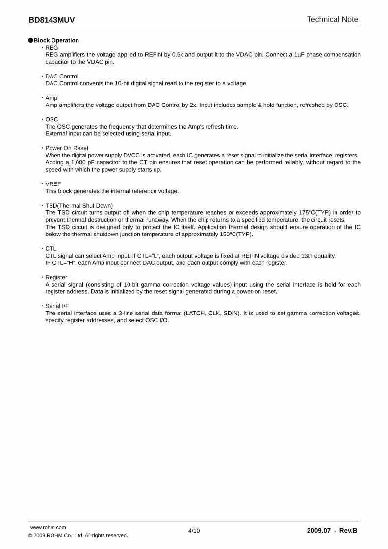
●Block Operation ・REG
REG amplifiers the voltage applied to REFIN by 0.5x and output it to the VDAC pin. Connect a 1µF phase compensation capacitor to the VDAC pin.
・DAC Control
DAC Control convents the 10-bit digital signal read to the register to a voltage. ・Amp
Amp amplifiers the voltage output from DAC Control by 2x. Input includes sample & hold function, refreshed by OSC. ・OSC
The OSC generates the frequency that determines the Amp's refresh time. External input can be selected using serial input.
・Power On Reset
When the digital power supply DVCC is activated, each IC generates a reset signal to initialize the serial interface, registers. Adding a 1,000 pF capacitor to the CT pin ensures that reset operation can be performed reliably, without regard to the speed with which the power supply starts up.
・VREF
This block generates the internal reference voltage. ・TSD(Thermal Shut Down)
The TSD circuit turns output off when the chip temperature reaches or exceeds approximately 175°C(TYP) in order to prevent thermal destruction or thermal runaway. When the chip returns to a specified temperature, the circuit resets. The TSD circuit is designed only to protect the IC itself. Application thermal design should ensure operation of the IC below the thermal shutdown junction temperature of approximately 150°C(TYP).
・CTL
CTL signal can select Amp input. If CTL=”L”, each output voltage is fixed at REFIN voltage divided 13th equality. IF CTL=”H”, each Amp input connect DAC output, and each output comply with each register.
・Register
A serial signal (consisting of 10-bit gamma correction voltage values) input using the serial interface is held for each register address. Data is initialized by the reset signal generated during a power-on reset.
・Serial I/F
The serial interface uses a 3-line serial data format (LATCH, CLK, SDIN). It is used to set gamma correction voltages, specify register addresses, and select OSC I/O.

Technical Note
5/10
BD8143MUV
www.rohm.com 2009.07 - Rev.B© 2009 ROHM Co., Ltd. All rights reserved.
●Serial Communication The serial data control block is composed of Shift-Register, DAC Register and DAC circuit. The DAC register memorizes data from the serial interface (LATCH, CLK and SDIN). The DAC circuit makes control voltage from the register output and it outputs to the each block. The DAC register value turns back the preset value when Power Supply starts up. Then, beginning 1bit of SDIN is always 0, because it is for test. Next 1bit switches OSC mode. If input 0, OSC mode is internal mode (the frequency is 100kHz). If input 1, it is external one that require external clock.
Fig.2 SERIAL BLOCK ①TIMING OF SERIAL COMMUNICATION
The 17 bits Serial data from SDIN terminal is loaded to Shift-Register at the rise edge of CLK, and these data is loaded to DAC Register at the rise edge of LATCH. If serial data period is less than 17 bits while LATCH state is LOW, the serial data is not memorized. If serial data period is more than 17 bits while LATCH state is LOW, last 17 bits are effective.
Fig.3 TIMING OF SERIAL COMMUNICATION
②SERIAL DATA The composition of SERIAL DATA INPUT(SDIN) First → → Last
d0 d1 d2 d3 d4 d5 d6 d7 d8 d9 d10 d11 d12 d13 d14 d15 d16
0 X Resister Address DATA
REGISTER NAME ADDRESS
FUNCTION PRESET VALUE
d2 d3 d4 d5 d6 d7~d16
Register 0 0 0 0 0 0 OUT0 Voltage of control 00 0000 0000
Register 1 0 0 0 0 1 OUT1 Voltage of control 00 0000 0000
Register 2 0 0 0 1 0 OUT2 Voltage of control 00 0000 0000
Register 3 0 0 0 1 1 OUT3 Voltage of control 00 0000 0000
Register 4 0 0 1 0 0 OUT4 Voltage of control 00 0000 0000
Register 5 0 0 1 0 1 OUT5 Voltage of control 00 0000 0000
Register 6 0 0 1 1 0 OUT6 Voltage of control 00 0000 0000
Register 7 0 0 1 1 1 OUT7 Voltage of control 00 0000 0000
Register 8 0 1 0 0 0 OUT8 Voltage of control 00 0000 0000
Register 9 0 1 0 0 1 OUT9 Voltage of control 00 0000 0000
Register 10 0 1 0 1 0 OUT10 Voltage of control 00 0000 0000
Register 11 0 1 0 1 1 OUT11 Voltage of control 00 0000 0000
Register 12(*) 0 1 1 0 0 - 00 0000 0000 (*)IF Register 12 is loaded at DATA=1010100000(2A0h), each output comply with each register regardless of CTL signal.
Shift Register
OUT0~12
Register
DAC
ADDRESS
DECORDE
SERIAL DATA CONTROL BLOCK
CLOCK CONTROL
LATCH
CLK
SDIN
10bit 5bit
d11
d10
d12
d13
d14
d15
TEST MODE
1bit
OSC
MODE
1bit
d16
d9
d8
d7
d6
d5
d4
d3
d2
d1
d0
TIMING OF SERIAL COMMUNICATION
LATCH
CLK
SDIN d0 d1 d2 d3 d4 d5 d6 d7 d8 d9 d10 d11 d12 d13 d14 d15 d16

Technical Note
6/10
BD8143MUV
www.rohm.com 2009.07 - Rev.B© 2009 ROHM Co., Ltd. All rights reserved.
SDIN
LATCH
CLK tLC
tSC
tWL tWH tCL tLA
●Serial Communication Timing Chart
Fig.4 ●Timing Standard Value
Parameter Symbol LIMIT
Unit Min. Typ. Max.
LATCH Set up time tLC 0.1 - - us
SDIN Set up time tSC 0.1 - - us
CLK “H” time tWH 0.1 - - us
CLK “L” time tWL 0.1 - - us
LATCH hold time tCL 0.1 - - us
LATCH “H” time tLA 0.6 - - us
●Setting γ-Correction
Formula (1) shows the relationship between γ output voltage (OUT0~OUT11) and DAC digital value.
Output Voltage(OUT0~OUT11)=({(DAC digital value +1)/1024}×(REFIN/2)‐10mV)×2.0025 ・・・(1)
●Power Supply Sequence Digital power supply DVCC must be supplied earlier than VCC for the prevent of wrong behavior. The serial data must be input after cancellation of “Power on Reset”. When turn off power supply, VCC must be done earlier than DVCC.
Fig.5 Power Supply Sequence ●Power Supply Sequence Standard Value
Parameter Symbol LIMIT
Unit Condition Min. Typ. Max.
Timing of serial data input tDS 100 - - μs Cct=1000pF
Timing of VCC ON tSV - 10 - μs
Timing of REFIN ON tVR 0 10 - μs
Timing of REFIN OFF tRV 0 10 - μs
Timing of VCC OFF tVD 0 10 - μs
VCC rise time tVCC 1 - - ms
DVCC
LATCH
CLK
SDIN
・・・
・・・
・・・
・・・
・・・
VCC ・・・
・・・
・・・
・・・
・・・
tDS tSV
tVD tVcc
REFIN ・・・
・・・
tVR tRV

Technical Note
7/10
BD8143MUV
www.rohm.com 2009.07 - Rev.B© 2009 ROHM Co., Ltd. All rights reserved.
●Data writing time for register Data writing time for register depend on frequency of CLK. Below formula shows data writing time for all registers. (Because data writing time for a register is needed at 17bit data + LATCH “H” time.)
18 CLK × ×12ch [µs]
●Refresh time of Amp input
Each Amp input have sample & hold function refreshed by OSC frequency (fosc). Below formula shows refresh cycle.
×12ch [µs] When internal OSC mode, fOSC=100kHz (Typ).
●Function of selecting Amp input This IC can select Amp input by CTL signal. If CTL=”L”, Amp input is connected to resistance division of REFIN voltage. IF CTL=”H”, connected to DAC output. When VCC(REFIN) supplies with CTL=”L”, it is possible to start up without opposite Voltage of each output. Then, if the CTL signal changes “H” after 1ms and over since VCC(REFIN) supplied and data send finished, start up sequence should be below Fig. (*Amp input is connected to DAC output not only by CTL=”H”, but also DATA=1010100000(2A0h) sended to Register 12. Also in this case, please send DATA=1010100000(2A0h) to Register 12 after 1ms and over since VCC(REFIN) supplied And output data send finished, at this time CTL=”L”.)
Fig.6 Selecting Amp input block diagram Fig.7 Start up sequence
fCLK [MHz]
1
fOSC [kHz]
1
x2
DAC
Control
VCC
OUT
CTL
VDAC
REFIN VCC
OUT1
OUT0
OUT2
OUT11
OUT10
Preset value
DAC value
CTL
Preset value DAC value

Technical Note
8/10
BD8143MUV
www.rohm.com 2009.07 - Rev.B© 2009 ROHM Co., Ltd. All rights reserved.
●Input Output Circuit (BD8143MUV) 1.LATCH 2.SDIN 3.CLK 4.SDOUT 6.CT
9.OSC 11. CTL
14.OUT0 15.OUT1 16.OUT2 17.OUT3 18.OUT4 19.OUT5 22.OUT6 23.OUT7 24.OUT8 25.OUT9 26.OUT10 27.OUT11
29.REFIN 30.VDAC
Fig.8
GND
GND
GND
VCC
AGND
DVCC
VCC
AGND
DVCC
GND
AGND
VCC
DVCC DVCC
DVCC
GND

Technical Note
9/10
BD8143MUV
www.rohm.com 2009.07 - Rev.B© 2009 ROHM Co., Ltd. All rights reserved.
(Pin A)
GND
N
P
N N
P+P+
Resistor
Parasitic elements P
~ ~ ~ ~
Parasitic elements
(Pin B)
GND
C B
E
Parasitic elements
GND
(Pin A)
~ ~
GND
N
P
N N
P+ P+
Parasitic elements
P substrate
(Pin B) C
B
E
Transistor (NPN)
~ ~
NGND
●Notes for use 1) Absolute maximum ratings
Use of the IC in excess of absolute maximum ratings such as the applied voltage or operating temperature range may result in IC damage. Assumptions should not be made regarding the state of the IC (short mode or open mode) when such damage is suffered. A physical safety measure such as a fuse should be implemented when use of the IC in a special mode where the absolute maximum ratings may be exceeded is anticipated.
2) GND potential Ensure a minimum GND pin potential in all operating conditions.
3) Setting of heat Use a thermal design that allows for a sufficient margin in light of the power dissipation (Pd) in actual operating conditions.
4) Pin short and mistake fitting Use caution when orienting and positioning the IC for mounting on printed circuit boards. Improper mounting may result in damage to the IC. Shorts between output pins or between output pins and the power supply and GND pins caused by the presence of a foreign object may result in damage to the IC.
5) Actions in strong magnetic field Use caution when using the IC in the presence of a strong magnetic field as doing so may cause the IC to malfunction.
6) Testing on application boards When testing the IC on an application board, connecting a capacitor to a pin with low impedance subjects the IC to stress. Always discharge capacitors after each process or step. Ground the IC during assembly steps as an antistatic measure, and use similar caution when transporting or storing the IC. Always turn the IC's power supply off before connecting it to or removing it from a jig or fixture during the inspection process.
7) Ground wiring patterns When using both small signal and large current GND patterns, it is recommended to isolate the two ground patterns, placing a single ground point at the application's reference point so that the pattern wiring resistance and voltage variations caused by large currents do not cause variations in the small signal ground voltage. Be careful not to change the GND wiring patterns of any external components.
8) Regarding input pin of the IC This monolithic IC contains P+ isolation and P substrate layers between adjacent elements in order to keep them isolated. P/N junctions are formed at the intersection of these P layers with the N layers of other elements to create a variety of parasitic elements. For example, when the resistors and transistors are connected to the pins as shown in below Fig.9, a parasitic diode or a transistor operates by inverting the pin voltage and GND voltage. The formation of parasitic elements as a result of the relationships of the potentials of different pins is an inevitable result of the IC's architecture. The operation of parasitic elements can cause interference with circuit operation as well as IC malfunction and damage. For these reasons, it is necessary to use caution so that the IC is not used in a way that will trigger the operation of parasitic elements such as by the application of voltages lower than the GND (P substrate) voltage to input and output pins.
Fig.9 Example of a Simple Monolithic IC Architecture 9) Overcurrent protection circuits
An overcurrent protection circuit designed according to the output current is incorporated for the prevention of IC damage that may result in the event of load shorting. This protection circuit is effective in preventing damage due to sudden and unexpected accidents. However, the IC should not be used in applications characterized by the continuous operation or transitioning of the protection circuits. At the time of thermal designing, keep in mind that the current capacity has negative characteristics to temperatures.
10) Thermal shutdown circuit (TSD) This IC incorporates a built-in TSD circuit for the protection from thermal destruction. The IC should be used within the specified power dissipation range. However, in the event that the IC continues to be operated in excess of its power dissipation limits, the attendant rise in the chip's junction temperature Tj will trigger the TSD circuit to turn off all output power elements. The circuit automatically resets once the junction temperature Tj drops.Operation of the TSD circuit presumes that the IC's absolute maximum ratings have been exceeded. Application designs should never make use of the TSD circuit.
11) Testing on application boards At the time of inspection of the installation boards, when the capacitor is connected to the pin with low impedance, be sure to discharge electricity per process because it may load stresses to the IC. Always turn the IC's power supply off before connecting it to or removing it from a jig or fixture during the inspection process. Ground the IC during assembly steps as an antistatic measure, and use similar caution when transporting or storing the IC.
12) Push Current This IC may rush current momentary by power supply order or delay, use caution about power supply coupling capacitor, width or routing of VCC ,GND patterns

Technical Note
10/10
BD8143MUV
www.rohm.com 2009.07 - Rev.B© 2009 ROHM Co., Ltd. All rights reserved.
●Ordering part number
B D 8 1 4 3 M U V - E 2
Part No. Part No.
Package
MUV: VQFN032V5050 Packaging and forming specification E2: Embossed tape and reel
(Unit : mm)
VQFN032V5050
0.08 S
S
1.0M
AX
(0.2
2)
0.02
+0.
03-
0.02
24
81
932
1625
17
0.5
0.75
0.4
±0.1
3.4±0.1
3.4
±0.1
0.25+0.05-0.04
C0.2
5.0±0.1
5.0
±0.1
1PIN MARK
∗ Order quantity needs to be multiple of the minimum quantity.
<Tape and Reel information>
Embossed carrier tapeTape
Quantity
Direction of feed
The direction is the 1pin of product is at the upper left when you hold reel on the left hand and you pull out the tape on the right hand
2500pcs
E2
( )
Direction of feed
Reel1pin

DatasheetDatasheet
Notice - GE Rev.002© 2014 ROHM Co., Ltd. All rights reserved.
Notice Precaution on using ROHM Products
1. Our Products are designed and manufactured for application in ordinary electronic equipments (such as AV equipment, OA equipment, telecommunication equipment, home electronic appliances, amusement equipment, etc.). If you intend to use our Products in devices requiring extremely high reliability (such as medical equipment (Note 1), transport equipment, traffic equipment, aircraft/spacecraft, nuclear power controllers, fuel controllers, car equipment including car accessories, safety devices, etc.) and whose malfunction or failure may cause loss of human life, bodily injury or serious damage to property (“Specific Applications”), please consult with the ROHM sales representative in advance. Unless otherwise agreed in writing by ROHM in advance, ROHM shall not be in any way responsible or liable for any damages, expenses or losses incurred by you or third parties arising from the use of any ROHM’s Products for Specific Applications.
(Note1) Medical Equipment Classification of the Specific Applications JAPAN USA EU CHINA
CLASSⅢ CLASSⅢ
CLASSⅡb CLASSⅢ
CLASSⅣ CLASSⅢ
2. ROHM designs and manufactures its Products subject to strict quality control system. However, semiconductor
products can fail or malfunction at a certain rate. Please be sure to implement, at your own responsibilities, adequate safety measures including but not limited to fail-safe design against the physical injury, damage to any property, which a failure or malfunction of our Products may cause. The following are examples of safety measures:
[a] Installation of protection circuits or other protective devices to improve system safety [b] Installation of redundant circuits to reduce the impact of single or multiple circuit failure
3. Our Products are designed and manufactured for use under standard conditions and not under any special or extraordinary environments or conditions, as exemplified below. Accordingly, ROHM shall not be in any way responsible or liable for any damages, expenses or losses arising from the use of any ROHM’s Products under any special or extraordinary environments or conditions. If you intend to use our Products under any special or extraordinary environments or conditions (as exemplified below), your independent verification and confirmation of product performance, reliability, etc, prior to use, must be necessary:
[a] Use of our Products in any types of liquid, including water, oils, chemicals, and organic solvents [b] Use of our Products outdoors or in places where the Products are exposed to direct sunlight or dust [c] Use of our Products in places where the Products are exposed to sea wind or corrosive gases, including Cl2,
H2S, NH3, SO2, and NO2
[d] Use of our Products in places where the Products are exposed to static electricity or electromagnetic waves [e] Use of our Products in proximity to heat-producing components, plastic cords, or other flammable items [f] Sealing or coating our Products with resin or other coating materials [g] Use of our Products without cleaning residue of flux (even if you use no-clean type fluxes, cleaning residue of
flux is recommended); or Washing our Products by using water or water-soluble cleaning agents for cleaning residue after soldering
[h] Use of the Products in places subject to dew condensation
4. The Products are not subject to radiation-proof design. 5. Please verify and confirm characteristics of the final or mounted products in using the Products. 6. In particular, if a transient load (a large amount of load applied in a short period of time, such as pulse. is applied,
confirmation of performance characteristics after on-board mounting is strongly recommended. Avoid applying power exceeding normal rated power; exceeding the power rating under steady-state loading condition may negatively affect product performance and reliability.
7. De-rate Power Dissipation (Pd) depending on Ambient temperature (Ta). When used in sealed area, confirm the actual
ambient temperature. 8. Confirm that operation temperature is within the specified range described in the product specification. 9. ROHM shall not be in any way responsible or liable for failure induced under deviant condition from what is defined in
this document.
Precaution for Mounting / Circuit board design 1. When a highly active halogenous (chlorine, bromine, etc.) flux is used, the residue of flux may negatively affect product
performance and reliability. 2. In principle, the reflow soldering method must be used; if flow soldering method is preferred, please consult with the
ROHM representative in advance. For details, please refer to ROHM Mounting specification

DatasheetDatasheet
Notice - GE Rev.002© 2014 ROHM Co., Ltd. All rights reserved.
Precautions Regarding Application Examples and External Circuits 1. If change is made to the constant of an external circuit, please allow a sufficient margin considering variations of the
characteristics of the Products and external components, including transient characteristics, as well as static characteristics.
2. You agree that application notes, reference designs, and associated data and information contained in this document
are presented only as guidance for Products use. Therefore, in case you use such information, you are solely responsible for it and you must exercise your own independent verification and judgment in the use of such information contained in this document. ROHM shall not be in any way responsible or liable for any damages, expenses or losses incurred by you or third parties arising from the use of such information.
Precaution for Electrostatic
This Product is electrostatic sensitive product, which may be damaged due to electrostatic discharge. Please take proper caution in your manufacturing process and storage so that voltage exceeding the Products maximum rating will not be applied to Products. Please take special care under dry condition (e.g. Grounding of human body / equipment / solder iron, isolation from charged objects, setting of Ionizer, friction prevention and temperature / humidity control).
Precaution for Storage / Transportation 1. Product performance and soldered connections may deteriorate if the Products are stored in the places where:
[a] the Products are exposed to sea winds or corrosive gases, including Cl2, H2S, NH3, SO2, and NO2 [b] the temperature or humidity exceeds those recommended by ROHM [c] the Products are exposed to direct sunshine or condensation [d] the Products are exposed to high Electrostatic
2. Even under ROHM recommended storage condition, solderability of products out of recommended storage time period may be degraded. It is strongly recommended to confirm solderability before using Products of which storage time is exceeding the recommended storage time period.
3. Store / transport cartons in the correct direction, which is indicated on a carton with a symbol. Otherwise bent leads
may occur due to excessive stress applied when dropping of a carton. 4. Use Products within the specified time after opening a humidity barrier bag. Baking is required before using Products of
which storage time is exceeding the recommended storage time period.
Precaution for Product Label QR code printed on ROHM Products label is for ROHM’s internal use only.
Precaution for Disposition When disposing Products please dispose them properly using an authorized industry waste company.
Precaution for Foreign Exchange and Foreign Trade act Since our Products might fall under controlled goods prescribed by the applicable foreign exchange and foreign trade act, please consult with ROHM representative in case of export.
Precaution Regarding Intellectual Property Rights 1. All information and data including but not limited to application example contained in this document is for reference
only. ROHM does not warrant that foregoing information or data will not infringe any intellectual property rights or any other rights of any third party regarding such information or data. ROHM shall not be in any way responsible or liable for infringement of any intellectual property rights or other damages arising from use of such information or data.:
2. No license, expressly or implied, is granted hereby under any intellectual property rights or other rights of ROHM or any
third parties with respect to the information contained in this document.
Other Precaution 1. This document may not be reprinted or reproduced, in whole or in part, without prior written consent of ROHM. 2. The Products may not be disassembled, converted, modified, reproduced or otherwise changed without prior written
consent of ROHM. 3. In no event shall you use in any way whatsoever the Products and the related technical information contained in the
Products or this document for any military purposes, including but not limited to, the development of mass-destruction weapons.
4. The proper names of companies or products described in this document are trademarks or registered trademarks of
ROHM, its affiliated companies or third parties.

DatasheetDatasheet
Notice – WE Rev.001© 2014 ROHM Co., Ltd. All rights reserved.
General Precaution 1. Before you use our Pro ducts, you are requested to care fully read this document and fully understand its contents.
ROHM shall n ot be in an y way responsible or liabl e for fa ilure, malfunction or acci dent arising from the use of a ny ROHM’s Products against warning, caution or note contained in this document.
2. All information contained in this docume nt is current as of the issuing date and subj ect to change without any prior
notice. Before purchasing or using ROHM’s Products, please confirm the la test information with a ROHM sale s representative.
3. The information contained in this doc ument is provi ded on an “as is” basis and ROHM does not warrant that all
information contained in this document is accurate an d/or error-free. ROHM shall not be in an y way responsible or liable for any damages, expenses or losses incurred by you or third parties resulting from inaccuracy or errors of or concerning such information.